Omron RFID Business Development Department V720SHMU01 RFID Transmitter User Manual
Omron Corporation, RFID Business Development Department RFID Transmitter
user manual

Electromagnetic Inductive
RFID System
V720-series
User’s Manual
USB Type RFID Unit
V720S-HMU01
Manual Number SRFM-017
OMRON Corporation
PRELIMINARY

ii
About this Manual:
This manual describes the installation and operation of the V720-series Electromagnetic Inductive
RFID System (V720S-HMU01) and includes the sections described below.
Please read this manual carefully and be sure you understand the information provided before
attempting to install and operate the System.
Section 1 provides the features of the V720S-HMU01.
Section 2 provides the specifications and performance characteristics of the V720S-HMU01.
Section 3 provides the functions and operations of the V720S-HMU01.
Section 4 provides the communications functions and provides details on communications–related
data and commands.
Section 5 provides the information of characteristics data.
Section 6 provides user application software samples.
* Prior to connect the RFID unit to the computer via USB, install the specified device driver into the
computer referring to the Section 6 of this manual.
Precautions
Read and Understand this Manual
Please read and understand this manual before using the products. Please consult your OMRON
representative if you have any questions or comments.
Warranty, Limitations of Liability
< WARRANTY >
OMRON's exclusive warranty is that the products are free from defects in materials and
workmanship for a period of one year (or other period if specified) from date of sale by OMRON.
OMRON MAKES NO WARRANTY OR REPRESENTATION, EXPRESS OR IMPLIED, REGARDING NON-INFRINGEMENT,
MERCHANTABILITY, OR FITNESS FOR PARTICULAR PURPOSE OF THE PRODUCTS. ANY BUYER OR USER
ACKNOWLEDGES THAT THE BUYER OR USER ALONE HAS DETERMINED THAT THE PRODUCTS WILL SUITABLY MEET
THE REQUIREMENTS OF THEIR INTENDED USE. OMRON DISCLAIMS ALL OTHER WARRANTIES, EXPRESS OR
IMPLIED.
< LIMITATIONS OF LIABILITY >
OMRON SHALL NOT BE RESPONSIBLE FOR SPECIAL, INDIRECT, OR CONSEQUENTIAL DAMAGES, LOSS OF PROFITS
OR COMMERCIAL LOSS IN ANY WAY CONNECTED WITH THE PRODUCTS, WHETHER SUCH CLAIM IS BASED ON
CONTRACT, WARRANTY, NEGLIGENCE, OR STRICT LIABILITY.
In no event shall the responsibility of OMRON for any act exceed the individual price of the
product on which liability is asserted.
IN NO EVENT SHALL OMRON BE RESPONSIBLE FOR WARRANTY, REPAIR, OR OTHER CLAIMS REGARDING THE
PRODUCTS UNLESS OMRON'S ANALYSIS CONFIRMS THAT THE PRODUCTS WERE PROPERLY HANDLED, STORED,
INSTALLED, AND MAINTAINED AND NOT SUBJECT TO CONTAMINATION, ABUSE, MISUSE, OR INAPPROPRIATE
MODIFICATION OR REPAIR.

iii
Application Considerations
< SUITABILITY FOR USE >
OMRON shall not be responsible for conformity with any standards, codes, or regulations that
apply to the combination of the products in the customer's application or use of the products.
At the customer's request, OMRON will provide applicable third party certification documents
identifying ratings and limitations of use that apply to the products. This information by
itself is not sufficient for a complete determination of the suitability of the products in
combination with the end product, machine, system, or other application or use.
The following are some examples of applications for which particular attention must be given.
This is not intended to be an exhaustive list of all possible uses of the products, nor is it
intended to imply that the uses listed may be suitable for the products:
z Outdoor use, uses involving potential chemical contamination or electrical interference,
or conditions or uses not described in this manual.
z Nuclear energy control systems, combustion systems, railroad systems, aviation systems,
medical equipment, amusement machines, vehicles, safety equipment, and installations
subject to separate industry or government regulations.
z Systems, machines, and equipment that could present a risk to life or property.
Please know and observe all prohibitions of use applicable to the products.
NEVER USE THE PRODUCTS FOR AN APPLICATION INVOLVING SERIOUS RISK TO LIFE OR PROPERTY WITHOUT
ENSURING THAT THE SYSTEM AS A WHOLE HAS BEEN DESIGNED TO ADDRESS THE RISKS, AND THAT THE OMRON
PRODUCTS ARE PROPERLY RATED AND INSTALLED FOR THE INTENDED USE WITHIN THE OVERALL EQUIPMENT
OR SYSTEM.
< PROGRAMMABLE PRODUCTS >
OMRON shall not be responsible for the user's programming of a programmable product, or any
consequence thereof.
Disclaimers
< PERFORMANCE DATA >
Performance data given in this manual is provided as a guide for the user in determining
suitability and does not constitute a warranty. It may represent the result of OMRON’s test
conditions, and the users must correlate it to actual application requirements. Actual
performance is subject to the OMRON Warranty and Limitations of Liability.

iv
< CHANGE IN SPECIFICATIONS >
Product specifications and accessories may be changed at any time based on improvements and
other reasons.
It is our practice to change model numbers when published ratings or features are changed, or
when significant construction changes are made. However, some specifications of the products
may be changed without any notice. When in doubt, special model numbers may be assigned to
fix or establish key specifications for your application on your request. Please consult with
your OMRON representative at any time to confirm actual specifications of purchased products.
< DIMENSIONS AND WEIGHTS >
Dimensions and weights are nominal and are not to be used for manufacturing purposes, even when
tolerances are shown.
< ERRORS AND OMISSIONS >
The information in this manual has been carefully checked and is believed to be accurate; however,
no responsibility is assumed for clerical, typographical, or proofreading errors, or omissions.
v
Safety Precautions
This chapter provides important information for the safe use of this product.
Ensure to read the information carefully before use.
In the safety precautions below, severity is categorized as either “WARNING” or “CAUTION”.
WARNING
Indicates a potentially hazardous situation which, if not avoided,
could result in death or serious injury.
Caution
Indicates a potentially hazardous situation which, if not avoided,
may result in minor or moderate injury, or property damage.
Property damage refers to extended damage caused to
house/household goods or livestock/pets.
●Description of Symbols
Prohibition
Indicates an action or activity not permitted.
Observe strictly
Indicates the need to ensure the safe use of the product.
Ensure to establish a solid grounding
A label indicating that a device with a grounding terminal should always be
grounded.
Electric shock hazard
A notification that alerts the possibility of electric shock under certain
conditions.
Do not disassemble
A notification that prohibits disassembly when injuries caused by electric
shocks may result.
Please ensure that all cautions and prohibitions are adhered to, since non-compliance may lead
to serious injury or damage, in certain circumstances.
vi
WARNING
Never disassemble, repair, or modify the main unit and cables.
z Do not disassemble, repair, or modify this product. Doing so may result in electric shock, fire, or
personal injury.
Caution
Do not drop the device or apply physical shock.
z Doing so may result in personal injury or device damage.
Do not apply strong force to, or place heavy items on the device or cables.
z Doing so may deform or damage the device, resulting in electric shock or fire.
Use and store the product in an environment that is specified in the catalog or
operation manual.
z Failure to do so may cause failure of the device, electric shock, or fire. Do not use or store the
device in the following locations:
・ Locations that do not satisfy the specified operating conditions (-10°C to +40°C, 25%RH to
85%RH,non-condensing).
・ Locations that do not satisfy the specified storage conditions (-25°C to +65°C, 25%RH to
85%RH,non-condensing).
・ Locations where the RFID Unit is exposed to direct sunlight.
・ Locations where the RFID Unit is exposed to dust, corrosive gas, saline, or flammable gas.
・ Locations where the RFID Unit is exposed to direct heat.
・ Locations subject to condensation due to high humidity.
・ Locations subject to vibration or impact that exceed the limits outlined in the
specifications.
・ Locations where the device may be exposed to water, oil, or chemical agents. (This
applies to the models other than waterproof types.)
・ Outdoor
z Store and carry the product in packed state.

vii
To avoid interferences with other systems, adhere to the following items and check
them before using the product.
z The product uses a publicly available ISM frequency band of 13.56 MHz to communicate with
Tags. Some transceivers, motors, monitoring devices, power supplies (power supply ICs), and
other similar RFID systems may generate noise, which cause radio interference and may affect
communication with Tags. If the product is required in the vicinity of these items, check for any
interference prior to use.
z On the contrary, the system itself may affect radio station transmissions or medical devices. Be
cautious when using the system in the environments where such effects might occur.
z To minimize noise effects, adhere to the following:
・
Establish a Class D grounding (former Class 3 grounding) for metal objects placed in the
vicinity of the system.
・
Keep cables away from those with high voltages or heavy currents.
Do not allow the device or cables to be soused or exposed to water.
z Doing so may result in electric shock, fire or failure of non-waterproof devices or cables.
Connect the enclosed USB cable to the product for power supply.
z Failure to do so may damage the device or generate noise that affects receiving apparatus such
as TV or radio.
Connect the enclosed USB cable only between this product and a computer.
z Do not extend or modify the connection with other USB cable or USB adaptor.
Handle the USB cable by the connector portion to prevent excessive stress on the
connector.
z Failure to do so may result in poor contact or damage the device.
Handle the USB cable by the connector portion to prevent excessive stress on the
connector.
z Failure to do so may result in poor contact or damage the device.
If the device fails or is exposed to water (non-waterproof devices or parts), or an
unusual smell, smoke, or sparks are detected, immediately refrain from using the
device and contact OMRON or a sales representative for service and repair.
z Continued use of the failed device may result in electric shock or fire.
Adhere following instruction to prevent the power supply or AC adaptor belonged
to the computer from affecting communication with tags.
z Keep the distances from the power supply or AC adaptor for the computer as described in 5-6
“Positional Relation Between Reader and Computer” when use the device.
This product is not suitable for simultaneous connection of multiple units.
z Two or more products can not operate connecting with one computer.

viii
Precautions
This chapter provides important information for international standards and copyright.
Ensure to read the information carefully before use.
V720S-HMU01 conform to the following laws and standards.
1) US standards
FCC Part 15 Subpart C: 2006
FCC ID: OZGV720SHMU01
This device complies with Part 15 of the FCC Rules. Operation is subject to the following two
conditions: (1) this device may not cause harmful interference, and (2) this device must accept any
interference received, including interference that may cause undesired operation.
FCC WARNING: Changes or modifications not expressly approved by the party responsible for
compliance could void the user’s authority to operate the equipment.
NOTICE: This equipment has been tested and found to comply with the limits for a Class B digital
device, pursuant to part 15 of the FCC Rules. These limits are designed to provide reasonable
protection against harmful interference in a residential installation.
This equipment generates, uses and can radiate radio frequency energy and, if not installed and
used in accordance with the instructions, may cause harmful interference to radio communications.
However, there is no guarantee that interference will not occur in a particular installation. If this
equipment does cause harmful interference to radio or television reception, which can be
determined by turning the equipment off and on, the user is encouraged to try to correct the
interference by one or more of the following measures:
-Reorient or relocate the receiving antenna
-Increase the separation between the equipment and receiver.
-Connect the equipment into an outlet on a circuit different from that to which the receiver is
connected.
-Consult the dealer or an experienced radio/TV technician for help.
2) Canadian standards
RSS-Gen Issue 1: September 2005
RSS-210 Issue 6: September 2005
IC Number: 850L-72HMU01
This device complies with RSS-Gen of IC Rules. Operation is subject to the following two conditions:
(1) this device may not cause interference, and (2) this device must accept any interference,
including interference that may cause undesired operation of this device.
©Copyright OMRON Corporation 2007. All rights reserved.
This document is protected by copyright and is intended solely for use in conjunction with the
product. Notify your OMRON representative before copying or reproducing this document in any
manner, for any other purpose
Declarations
TABLE OF CONTENTS
ix
SECTION 1
Product Outline.......................................................................... 1-1
1-1 Features ........................................................................................................................ 1-2
SECTION 2
Specifications and Performance ............................................... 2-1
2-1 Nomenclature and Descriptions ................................................................................. 2-2
2-2 Specifications................................................................................................................ 2-4
2-2-1 General Specifications................................................................................................. 2-4
2-2-2 Interface Specifications ............................................................................................... 2-4
2-3 Dimensions ................................................................................................................... 2-5
SECTION 3
RIFD Unit Operations............................................................... 3-1
3-1 Outline of Operations.................................................................................................. 3-2
3-2 Tag Access Functions................................................................................................... 3-3
3-2-1 Tag Memory Map ........................................................................................................ 3-3
3-2-2 Single Access and FIFO Access Functions................................................................. 3-8
3-2-3 Lock Function .............................................................................................................. 3-9
SECTION 4
Controlling the RFID Unit ........................................................4-1
4-1 Communications Frames ............................................................................................ 4-2
4-1-1 CR Control ................................................................................................................... 4-2
4-2 Data Formats ............................................................................................................... 4-3
4-2-1 Command Code List.................................................................................................... 4-3
4-2-2 Communications Options ........................................................................................... 4-5
4-2-3 End Code List .............................................................................................................. 4-9
4-3 Commands and Responses during CR Control ........................................................ 4-10
4-3-1 General Commands (Commands sent to RFID Unit) .............................................. 4-10
4-3-2 Commands Common to the I-CODE1 and the I-CODESLI Chips ........................ 4-11
4-3-3 Commands Specific to the I-CODESLI Chip ........................................................... 4-15
4-3-4 Commands Specific to the I-CODE1 Chip................................................................ 4-18
4-3-5 Old Commands Specific to the I-CODE1 Chip ........................................................ 4-20
SECTION 5
Characteristics Data (Reference).............................................. 5-1
5-1 Communications Distance (Reference)...................................................................... 5-2
5-2 Diagram of Communications Range (Reference) ..................................................... 5-3
5-3 Communications Time (Reference)............................................................................ 5-6
5-3-1 Communications time ................................................................................................. 5-6
5-3-2 TAT (Turn Around Time)............................................................................................ 5-8
5-4 Effects of Surrounding Metal (Reference)................................................................. 5-9
5-5 Mutual Interference (Reference)................................................................................ 5-10
5-6 Positional Relation Between the Reader and the Computer (Reference) ............... 5-11
SECTION 6
Driver Installation ....................................................................6-1
6-1 Before installation........................................................................................................ 6-2
6-2 Driver Installation ....................................................................................................... 6-3
1-1
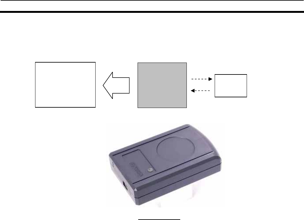
SECTION 1
Product Outline
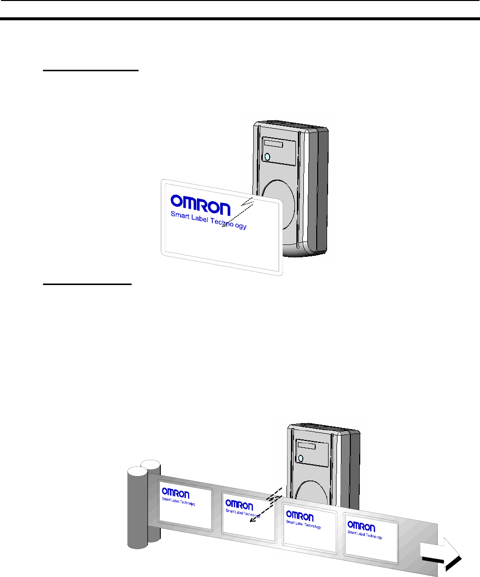
The RFID Unit is a unit, which includes an antenna PCB and a control PCB with control and send-receive
functions for communicating with OMRON V720-series Tags that use two types of Phillips Semiconductor
I-CODE chips (product name: SL1 ICS30 01, commonly known as "I-CODE1", and product name: SL2 ICS20,
commonly known as I-CODESLI); it also supports USB interface (USB2.0). The SL2 ICS20 chip fully conforms
to ISO/IEC15693.
1-1 Features...................................................................................................................1-2
1-1 Features
Section 1-1
1-2
1-1 Features
Compact Body
• 80 x 50 x t19.5mm
Baud Rate and Communication Control Method for communicating with the Host Control Unit
• The USB interface enables simple connection to the computer.
• With the specified device driver, the reader works as a virtual COM port.
• The baud rate in use is 9,600 bps (as a virtual COM port).
• A normal CR control is used as the communications control method.
(Note: the number-of-characters control method is not supported)
User-friendly Command Structure
• Easy-to-understand command structure.
• Built-in repetitive data write command (enabled when writing identical
data to tag memory areas).
• Specifiable data code (hexadecimal or ASCII) using read/write
command.
Many Operating Modes
• Supports two operating modes -- single access mode and FIFO access
mode -- according to the status of the tags within the communications
range.
• Support for four communication modes according to the communication
method with the Tag (three types in single access mode; Trigger, Auto,
and Repeat).
Computer
(Personal Computer)
RFID Unit
V720S-HMU01
V720 series
Tag
USB
2.0
V720S-HMU01
2-1
SECTION 2
Specifications and Performance
2-1 Nomenclature and Descriptions ...........................................................................2-2
2-2 Specifications .........................................................................................................2-4
2-2-1 General Specifications...........................................................................................2-4
2-2-2 Interface Specifications .........................................................................................2-4
2-3 Dimensions .............................................................................................................2-5
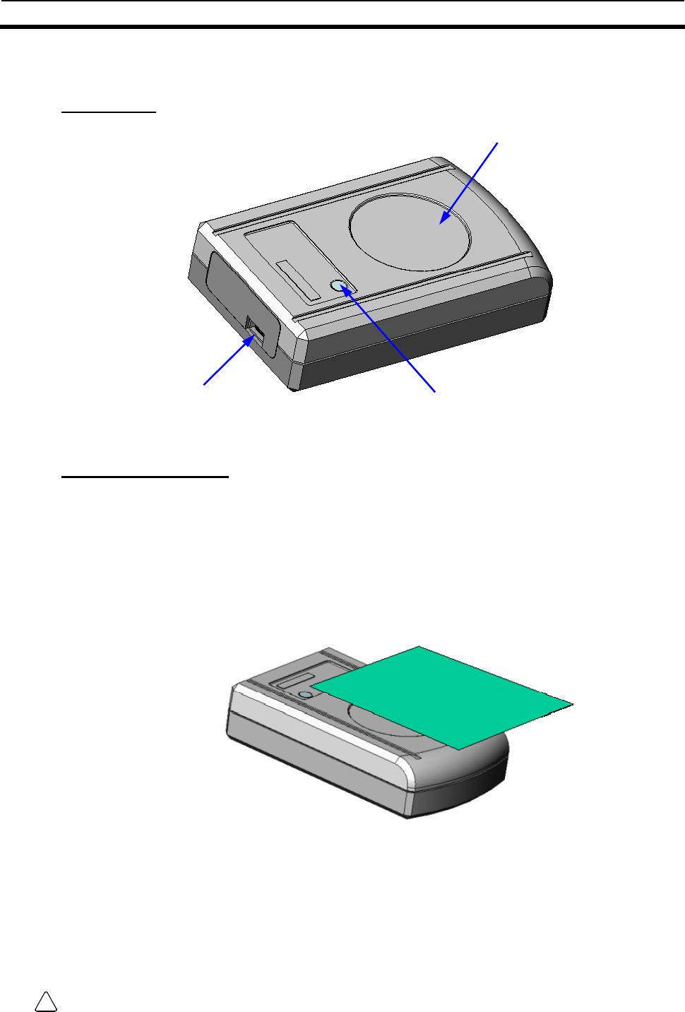
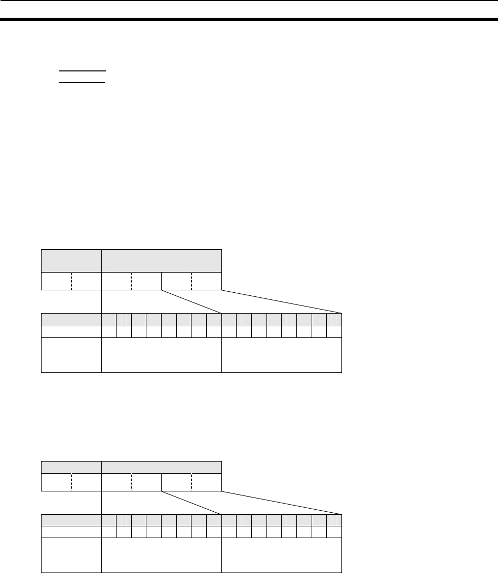
2-1 Nomenclature and Descriptions
Section 2-1
2-2
2-1 Nomenclature and Descriptions
V720S-HMU01
Component Descriptions
• USB Connector (USB Connector Mini B type)
To connect to the computer, insert USB cable here. The USB interface is conforms to USB 2.0.
• Antenna
To read tag data, set the tags near the antenna area as shown below.
The communication surface (antenna surface) is the top.
• LED Indicator
When the reader is communicating with the tag, the LED light is on.
Caution As the antenna is built in at the top of the RFID Unit, the direction of communication with the
tag is the upward.
!
USB Connector LED Indicator
Antenna

2-2 Specifications
Section 2-2
2-3
2-2 Specifications
2-2-1 General Specifications
Item V720S-HMU01
Dimensions 80 × 50 × t 19.5 mm
Mounting method Set on a flat surface
Power supply voltage 5.0 VDC (USB bus power)
Current consumption 100 mA max.
Vibration resistance Destruction: 10 to 150 Hz, 0.1-mm half amplitude at 15 m/s² in X, Y, and Z directions 10
times each for 8 minutes
Shock resistance Destruction: 150 m/s² three times each in 6 directions
Ambient operating
temperature -10 to +40℃
Ambient storage
temperature -25 to +65℃
Ambient operating
humidity 25%RH to 85%RH max. (with no condensation)
Communications
frequency 13.56 MHz
Weight Approx. 40 g
Radio standards
Extremely low power radio station (Radio Law Article 4 Section 1 radio stations that
discharge extremely low electric waves and specified by the Ministry of Posts and
Telecommunications) In accordance with Radio Law enforcement regulation Article
6 Section 1, the field intensity is 500µV/m or less at distance of 3 m (322 MHz or less).
*1
For the information of communications distance and area, refer to the data in 5-1 and 5-2 of section 5.
2-2-2 Interface Specifications
Item Details
Connectors USB mini B Connector
Communications
method 2-wire half duplex serial (appears as a virtual COM port on USB )
Synchronous method Asynchronous mode or start-stop synchronous mode
Communications
control method CR control (Number-of-characters control is not supported)
Baud rate 9,600 bps (Full speed device 12Mbps as a USB device)
Character format Start bits Data bits Parity Stop bits Total bits
1 8 Even 1 11
Error detection
method Parity
Bit send order Least significant bit (LSB) first
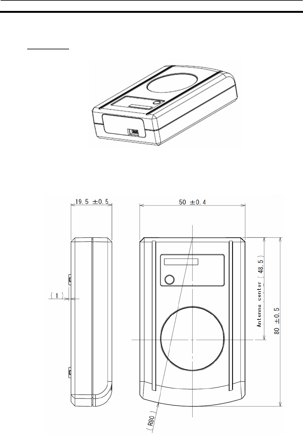
2-3 Dimensions
Section 2-3
2-4
2-3 Dimensions
V720S-HMU01
3-1
SECTION 3
RFID Unit Operations
3-1 Outline of Operations.............................................................................................3-2
3-2 Tag Access Functions............................................................................................3-3
3-2-1 Tag Memory Map...............................................................................................3-3
3-2-2 Single Access and FIFO Access Functions ......................................................3-8
3-2-3 Lock Function....................................................................................................3-9
3-1 Outline of Operations
Section 3-1
3-2
3-1 Outline of Operations
The RFID Unit reads or writes to the tags using commands sent from the host
control unit, and returns the processing responses to the host control unit.
The RFID Unit has three operating modes. The conditions for changing the
mode are shown in the following diagram.
(1) Command waiting mode
In this mode, the COM port is open and ready to receive a command as a
virtual COM port.
(2) Oscillation mode This mode performs communications with the tags.
When using FIFO access mode, oscillation mode continues until a STOP
command or STOP signal is input.
(3) Standby mode In this mode, the COM port is closed as a virtual COM port.
Note As the first step, open the COM port so that the RFID unit will shift its mode from “Standby
mode” to the “Command waiting mode”.
Control Unit
(Computer)
RFID Unit
V720S-HMU01
V720 series
Tag
Command waiting
mode
Standby mode
Oscillation mode
COM Port
Close
COM Port
Open Responses to
host sent
Commands from
host received
Command
Response

3-2 Tag Access Functions
Section 3-2
3-3
3-2 Tag Access Functions
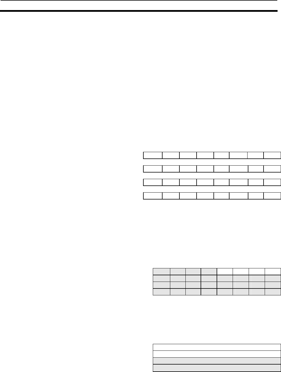
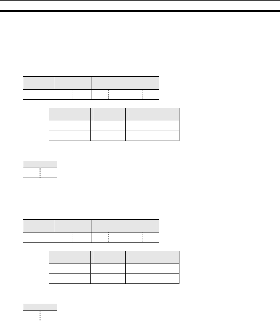
3-2-1 Memory Map of Tag
3-2-1-1 I-CODE1 Chip (Philips IC product name : SL1 ICS30 01, SL ICS31 01)
1) Memory Map of I-CODE1
These specifications describe a Tag incorporating an IC chip I- CODE1 Label
IC from Philips, which is accessed by the system.
This chip consists of a 64-byte memory. The upper five blocks (Blocks 0 to 4)
of the memory are used as a system area having functions that do not relate to
user memory. OMRON offers special commands for accessing this area in
order to ensure the great ease of these functions by the user.
Refer to Command List for details. OMRON defines the blocks below Block 5
as the user memory area. Block 5 is page 00h, and the subsequent blocks are
allocated as shown below.
The memory is organized with four bytes as one page (4 bytes = 32 bits).
One page is the minimum unit that can be read from and written to the
memory.
The memory allocation described in this user's manual is in accordance with
OMRON's memory allocation scheme.
OMRON PHILIPS
Bank Page Byte 0 Byte 1 Byte 2 Byte 3 Block
B Hex SNR 0
C Hex SNR 1
D Hex Write-protect 2
E Hex QUIET/EAS 3
F Hex Family code/application ID or user area 4
0 Hex User area 5
1 Hex 6
00 Hex 2 Hex 7
3 Hex 8
4 Hex 9
5 Hex 10
6 Hex 11
7 Hex 12
8 Hex 13
9 Hex 14
A Hex 15
Special Note Block 4 can be used as part of the user memory when the Distinguished Tag
Read/Write function by family code (FC) or application ID (AI) is not used. If such use is
preferred, define this page as F Hex to use it as part of the user memory. In this case,
the user memory area becomes 12 pages long.
3-2 Tag Access Functions
Section 3-2
3-4
2) System Area of I-CODE1
The system area of I-CODE1 is mapped onto the memory. OMRON allocates
the system area to pages B Hex to F Hex.
(1) SNR(pages C Hex, B Hex)
SNR is a tag-specific code and has been written into the memory during the
chip production process.
The RFID Unit is shipped with this page write-access inhibited (refer to page D
Hex); there is no way of making this page rewritable by the user.
(2) Write-access conditions (page D Hex)
The pages are write-inhibited permanently if they are so indicated in the
memory map. The factory settings are as follow. If the two bits of a particular
page are 0.0, that page is write-protected.
Page
D Hex MSB LSB
Byte 0 1 1 1 1 0 0 0 0
Page E Hex Page D Hex Page C Hex Page B Hex
Byte 1 1 1 1 1 1 1 1 1
Page 2 Hex Page 1 Hex Page 0 Hex Page F Hex
Byte 2 1 1 1 1 1 1 1 1
Page 6 Hex Page 5 Hex Page 4 Hex Page 3 Hex
Byte 3 1 1 1 1 1 1 1 1
Page A Hex Page 9 Hex Page 8 Hex Page 7 Hex
(3) QUIET/EAS (page E Hex)
QUIET mode: All the functions of a tag are suspended completely. Use Reset
Quiet Bit to resume these functions. (q=0: QUIET mode disabled; q=1: QUIET
mode enabled)
EAS mode: inhibition/permission of EAS function
(e=0: EAS mode disabled; e=1: EAS mode enabled)
Page Eh MSB LSB
Byte 0 × × × × q q e e
Byte 1 × × × × × × × ×
Byte 2 × × × × × × × ×
Byte 3 × × × × × × × ×
The pages marked with "×" in the table above are reserved for future use.
(4) Family code/application ID (page F Hex)
Family code and application ID are special areas for enabling the user to
identify an IC that is suitable to a specific user application.
Block Eh MSB LSB
Byte 0 Family code
Byte 1 Application ID
Byte 2 User area
Byte 3 User area
3-2 Tag Access Functions
Section 3-2
3-5
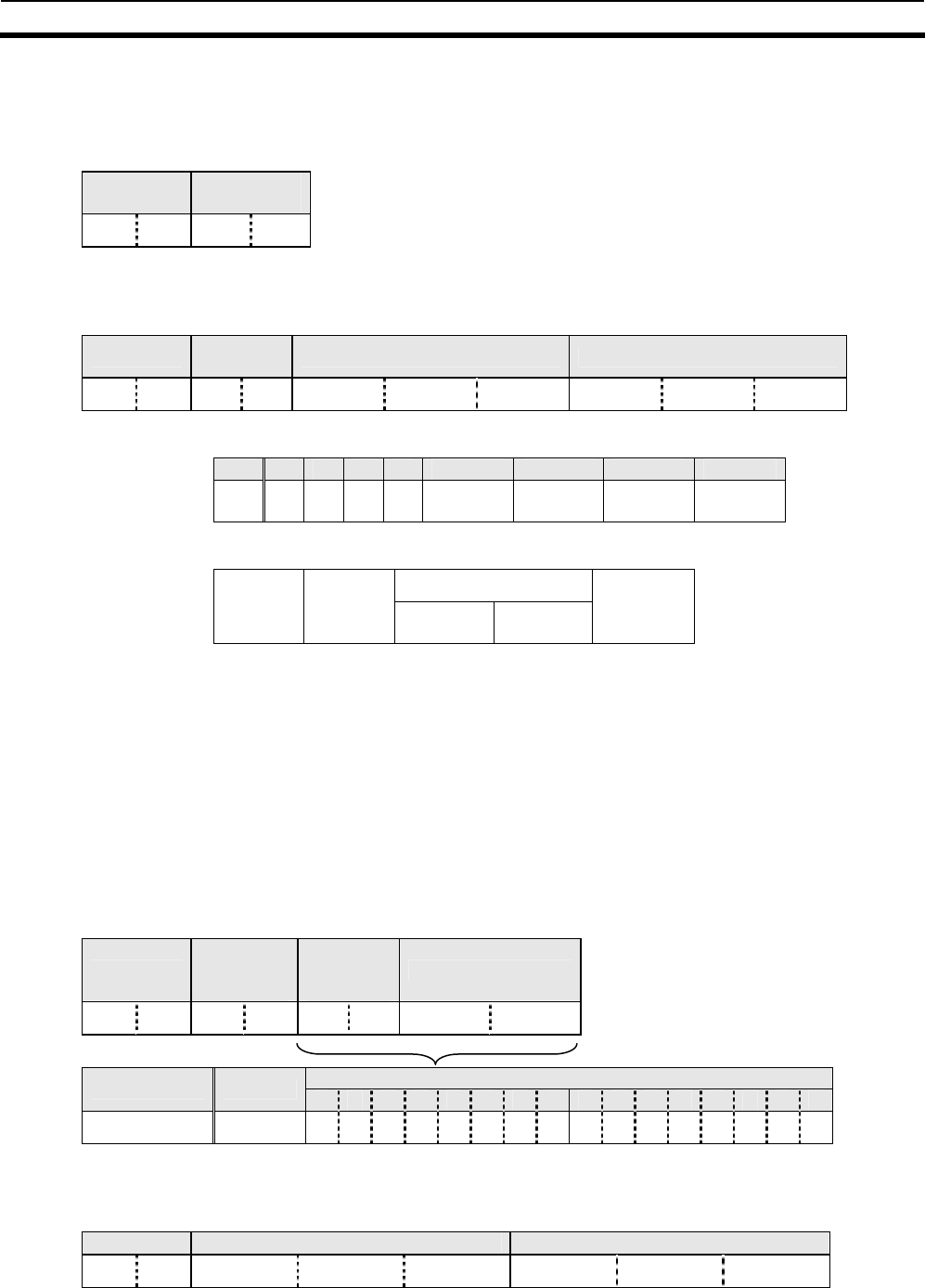
3-2-1-2 I-CODESLI Chip (Philips IC product name : SL2 ICS20)
In this module, processing is performed with the minimum access unit of one
page (4 bytes), the maximum number of pages that can be processed
simultaneously being one bank (16 pages), and up to a total of 16 banks (266
pages) being accessible.
The I-CODE 2 user memory area spans 112 bytes, or 28 pages, from page 00
Hex to page 1B Hex.
1) Max. address space of ISO/IEC15693 chip with a 4 Bytes/page organization
Bank Page Block Byte 0 Byte 1 Byte 2 Byte 3
0 Hex 0
1 Hex 1
2 Hex 2
3 Hex
4 Hex
5 Hex
6 Hex
7 Hex
8 Hex
9 Hex
A Hex
00 Hex
F Hex 15
0 Hex 16
1 Hex 17
B Hex 27
01 Hex
F 31
0 Hex 240
1 Hex 241
0F Hex
F Hex 255
Caution The memory map above shows a memory area covered by the product. It complies with the
ISO/IEC15693 standard.
Proper operation is ensured for our Tag, which incorporates Philips' IC product SL2ICS20
(known as "I-CODESLI"), although this product incorporates a firmware allowing to access
chips with a four bytes/page organization and fully compliant to ISO/IEC15693. Perform
check test adequately when using other company’s tag or tags that incorporate other
ISO/IEC15693 chips.
I-CODESLI
user memory area
Page 00 Hex to 1B Hex
(28 pages =112 bytes)
!
3-2 Tag Access Functions
Section 3-2
3-6
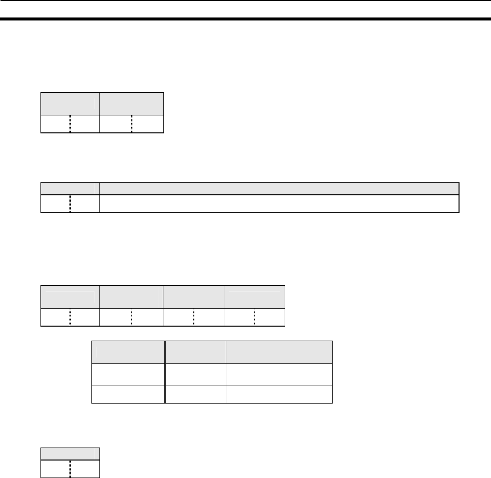
2) System Area of I-CODESLI
The I-CODESLI system area of is reserved in an area different from the user
memory.
Special commands are used for accessing the system area.
Byte 0 Byte 1 Byte 2 Byte 3
UID
UID
EAS/AFI/DSFID
Write-protect
(1)
UID UID is a tag-specific code and has been written into the memory during the
chip production process.
The RFID Unit is shipped with this page write-access inhibited; there is no way
of making this page rewritable by the user.
(2)
EAS/AFI/DSFID EAS mode: Inhibition/permission of EAS function
(e=0: EAS mode disabled; e=1: EAS mode enabled)
MSB LSB
Byte 1 × × × × × × × e
The pages marked with "×" in the table above are reserved for future use.
(3)
AFI AFI is a special area for enabling the user to identify a tag that is suitable to a
specific user application.
MSB LSB
Byte 2 AFI upper 4 bits AFI lower 4 bits
AFI upper
4 bits AFI lower
4 bits Application area Example/reference
0 0 All areas Area not identified
X 0 X area Selected extensively
X Y Y category of X area
0 Y Limited to Y category
1 0,Y Transportation
Mass-transit, bus, air plane
2 0,Y Finance Bank
3 0,Y Recognition Access control
4 0,Y Telecommunication Public telephone, CSM
5 0,Y Medical care
6 0,Y Multimedia Internet
7 0,Y Game
8 0,Y Data storage Portable file
9 0,Y Logistics
A 0,Y Home delivery services
B 0,Y Mail
C 0,Y Airplane luggage
D 0,Y Reservation
E 0,Y Reservation
F 0,Y Reservation
*Remarks: X=1 to F Y=1 to F

3-2 Tag Access Functions
Section 3-2
3-7
(4)
DSFID DSFID indicates how the data is configured in the memory.
MSB LSB
Byte 3 DSFID
(5)
Write-access conditions
The pages are write-inhibited permanently if they are so indicated in the
memory map. The factory settings are as follow. If the bit of a particular page is
1, that page is write-protected.
MSB LSB
Byte 0 0 0 0 0 0 0 0 0
Page
03 Page
02 Page
01 Page
00
Byte 1 0 0 0 0 0 0 0 0
Page
0B Page
0A Page
09 Page
08 Page
07 Page
06 Page
05 Page
04
Byte 2 0 0 0 0 0 0 0 0
Page
13 Page
12 Page
11 Page
10 Page
0F Page
0E Page
0D Page
0C
Byte 3 0 0 0 0 0 0 0 0
Page
1B Page
1A Page
19 Page
18 Page
17 Page
16 Page
15 Page
14
3-2 Tag Access Functions
Section 3-2
3-8
3-2-2 Single Access and FIFO Access Functions
Single Access Mode Use this mode to communicate with only one tag within the RFID Unit
communications area.
The time required for communications with the tag is shorter compared with
FIFO access mode.
FIFO Access Mode FIFO (First In First Out) access mode enables reading tags in order as they
enter the antenna communications range. Tags with which communications
have been completed are prohibited from being accessed again, so even if
tags with which communications have been completed are still within range of
the antenna, communications will be possible with new tags as they enter the
communications range. When two or more tags enter the antenna
communications range at the same time, a communications error will occur.
When a tag to which access has been prohibited moves out of the
communications area, communications with it will be possible again if it
reenters the antenna communications range.
The above diagram shows an example of a tag inspection line.
When the distance between tags is small, two tags may enter the RFID Unit
communications range at the same time. If this happens when in Single
Access Mode, a communications error will occur, or even if read/write appears
to have been performed, there is no way to know which of the two tags was
read. In FIFO Access Mode, tags entering communications range can be read
or written to in order, so this mode is suited to applications such as a tag
inspection line, in which the order of access is important.

3-2 Tag Access Functions
Section 3-2
3-9
3-2-3 Lock Function
The lock function is a protection function provided to prevent the loss of data
by unintentionally overwriting fixed data stored on the tags. This function can
be set using the lock command. This function can be set using the lock
command.
There is a lock setting area in the tag system area, enabling user-defined
areas to be write-protected one page at a time. If the write command is
executed for a page that has been write-protected, a write processing error will
occur.
Note The lock function used with the V720 Series cannot be canceled. Pages that have been
write-protected cannot be written to again, so be careful when using this function.

4-1
SECTION 4
Controlling the RFID Unit
4-1 Communications Frames ..............................................4-2
4-1-1 CR Control ...........................................................4-2
4-2 Data Formats .........................................................4-3
4-2-1 Command Code List ...................................................4-3
4-2-2 Communications Options...............................................4-5
4-2-3 End Code List ........................................................4-9
4-3 Commands and Responses during CR Control...........................4-10
4-3-1 General Commands (Commands sent to RFID Unit) .......................4-10
4-3-2 Commands Common to the I-CODE1 and the I-CODESLI Chips.............4-11
4-3-3 Commands Specific to the I-CODESLI Chip...............................4-15
4-3-4 Commands Specific to the I-CODE1 Chip.................................4-18
4-3-5 Old Commands Specific to the I-CODE1 Chip .............................4-20
Caution
The method for controlling the RFID Unit from the host control unit is the CR control method.
CR control Data in the communications frame is handled as ASCII characters in 2-digit hexadecimal
code (ASCII code). CR control simplifies operations with the host.
In this manual, the codes are displayed as follows:
ASCII characters: ’ ×× ‘
Control code using ASCII characters: ‘<Control code>‘
Displayed as hexadecimal code: ×× Hex
!
4-1 Communications Frames
Section 4-1
4-1 Communications Frames
4-1-1 CR control
The frame format consists of data in ASCII characters and a terminator. '<CR>' (ASCII: 0D Hex), the
terminator, cannot be used in the data ASCII characters.
The CR control method is useful when the RFID Unit is connected to a PC and the like.
Data 1 Data 2 ⋅⋅⋅⋅⋅⋅ Data n Terminator
Data No. of
characters Details
Data 1 to 138 Command parameters (ASCII characters)
Terminator 1 Code ‘<CR>‘ (0D Hex), which indicates end of communications
frame
(Communications Control Procedure)
When a character is first received, reception starts, and when <CR> is received, the frame ends. If the
interval between data is greater than 2 sec, a communications error occurs. If a communications error
occurs, a frame error end code (Error code: '18') is sent as the response from the RFID Unit to the host.
Data: 138 characters max
4-2 Data Formats
Section 4-2
4-3
4-2 Data Formats
The data in the communications frames used for commands and responses use the following formats.
Command
The command data consists of the command, communications options, and parameters. The commu-
nications options are added only to commands 01 to 03.
Command Communications
option Parameter 1 ⋅⋅⋅⋅⋅⋅ Parameter n
Response
The response data consists of an end code and parameters.
End code Parameter 1 ⋅⋅⋅⋅⋅⋅ Parameter n
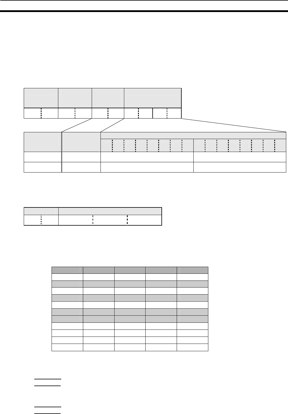
4-2-1 Command Code List
Commands specify RFID Unit processing. The commands are given in the following table.
1) General Commands (Commands sent to the RFID Unit)
Command name No. Details
Test 10 Sends the received data to the host device.
ACK 11 The host device received the data properly.
NACK 12 The host device did not receive the data properly.
STOP 13 Ends the command currently being executed.
Stops antenna oscillation.
2) Commands Common to the I-CODE1 and the I-CODESLI Chips
Command name No. Details
Read 31 Reads tag memory data on a page basis.
Write 32 Writes data to tag memory on a page basis.
Write identical data 33 Writes identical data to tag memory on a page basis.
Read UID (SNR) 35 Reads tag serial numbers.
Set write-protection 39 Sets write-protection on a page basis
3) Commands Specific to the I-CODESLI Chip
Command name No. Details
Set AFI 36 Overwrites and locks tag AFI.
Set DSFID 37 Overwrites and locks tag DSFID.
Read Tag info 3A Reads tag system information.
Read UID & data 41 Reads tag UID and memory data simultaneously.
EAS Alarm 42 Sends EAS Alarm to the tag.
Set EAS 43 Enables/disables and locks EAS.
4) Commands Specific to the I-CODE1 Chip
Command name No. Details
Read SNR 05 Reads tag serial numbers.
Read Family
Code and Appli-
cation ID
06 Reads tag family codes and application IDs.
Set Family Code
and Application ID
07 Writes tag family codes and application IDs.
Set EAS 08 Permits/prohibits EAS commands to the tags.
EAS 24 Sends EAS commands to the tags.

4-2 Data Formats
Section 4-2
4-4
5) Old Commands Specific to the I-CODE1 Chip (replaced by the Commands Common to the I-CODE1
and the I-CODESLI Chips)
Command name No. Details
Read 01 Reads tag memory data on a page basis.
Write 02 Writes data to tag memory on a page basis.
Write identical data 03 Writes identical data to tag memory on a page basis.
Set write-protection 09 Sets write-protection on a page basis.
4-2 Data Formats
Section 4-2
4-5
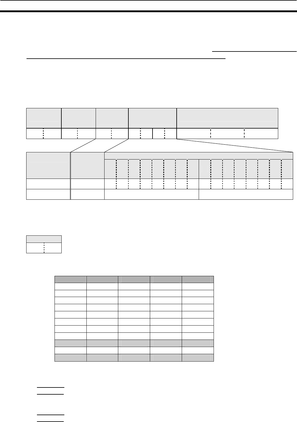
4-2-2 Communications Options
The data code and communications mode can be specified as communications options. Data code
specification is possible only when using CR control.
Bit 7 6 5 4 3 2 1 0
Setting
details 0 0 Tag type Data
code Communications mode
*Bits 6 and 7 must be 0.
1) Specifying Tag Type
Setting Value Details
I・CODE1 0 When accessing a tag equipped with I-CODE1
ISO/IEC15693
(4byte/page type) 1
When accessing a tag equipped with I-CODESLI
Addendum: when accessing the tag equipped with a chip with a
four bytes/page organization and fully conforming to
ISO/IEC15693
2) Specifying Data Code
Using CR Control
Specify the data code to perform read/write communications between the RFID Unit and the host control
unit. The specification concerns the data to be written/read to/from the user memory, as well as the test
data.
Setting Val
ue Details
Two-character data consisting of 0 to 9 and A to F is handled as 2-digit
hexadecimal data. Two characters occupy one byte of tag memory.
Example: When 12345678 is written to page 0, tag memory is used as
shown below.
Byte 0 12
Byte 1 34
Byte 2 56
Byte 3 78
Hex
0
Page 0
One character of data occupies one byte of tag memory as ASCII or JIS8
unit code.
Example: When ‘ABCD’ is written to page 0, tag memory is used as shown
below.
Byte 0 41
Byte 1 42
Byte 2 43
Byte 3 44
ASCII
1

4-2 Data Formats
Section 4-2
4-6
3) Specifying the Communications Mode
The following seven communications modes are supported for different processing procedures and
execution timing.
Communica-
tions mode No. Details
Single Trigger 0 Hex
After a command is received, communications with the tag is performed immediately
and a response is sent. If there is no tag in communications range, a No Tag error is
sent. After the response has been sent, the mode changes to sleep mode.
Only one tag is permitted in communications range.
Single Auto 1 Hex
After a command is received, this mode waits for a tag to enter communications
range, and then performs communications with the tag. After the response has
been sent, the mode changes to sleep mode. If a STOP command is received
while waiting for a tag, the command is ended.
Only one tag is permitted in communications range.
Single Repeat 2 Hex
After a command is received, this mode waits for a tag to enter communications
range, and then performs communications with the tag. If this mode has been
specified, the command is repeated sequentially until a STOP command is re-
ceived. This mode is enabled only for read commands.
Only one tag is permitted in communications range.
FIFO Trigger 8 Hex
After a command is received, communications with the tag is performed imme-
diately and a response is sent. If there is no tag in communications range, a No
Tag error is sent. Access is prohibited to tags with which communications have
been completed, and the RFID Unit continues unmodulated oscillation. Tags with
which communications have been completed do not respond to the next com-
mand. After the response has been sent, the mode changes to sleep mode. If a
STOP command is received, oscillation stops.
FIFO Auto 9 Hex
After a command is received, this mode waits for a tag to enter communications range,
and then performs communications with the tag. Access is prohibited to tags with which
communications have been completed, and the RFID Unit continues unmodulated
oscillation. Tags with which communications have been completed do not respond to
the next command. After the response has been sent, the mode changes to sleep
mode. If a STOP command is received while waiting for a tag, the command is ended.
FIFO Continu-
ous A Hex
After a command is received, this mode waits for a tag to enter communications range,
and then performs communications with the tag. Access is prohibited to tags with which
communications have been completed, and the RFID Unit continues unmodulated
oscillation. Tags with which communications have been completed do not respond to
the next command. After the response has been sent, when ACK is received, this mode
again waits for a tag to enter communications range, and then performs communica-
tions with the tag. If a STOP command is received while waiting for a tag, the command
is ended.
FIFO Repeat B Hex
After a command is received, this mode waits for a tag to enter communications range,
and then performs communications with the tag. Access is prohibited to tags with which
communications have been completed. Tags with which communications have been
completed do not respond to the next command. If this mode has been specified, the
command is repeated sequentially until a STOP command is received.
Note Single repeat mode can only be specified for commands 01, 31, 35, 3A, 41, and 42.
4-2 Data Formats
Section 4-2
4-7
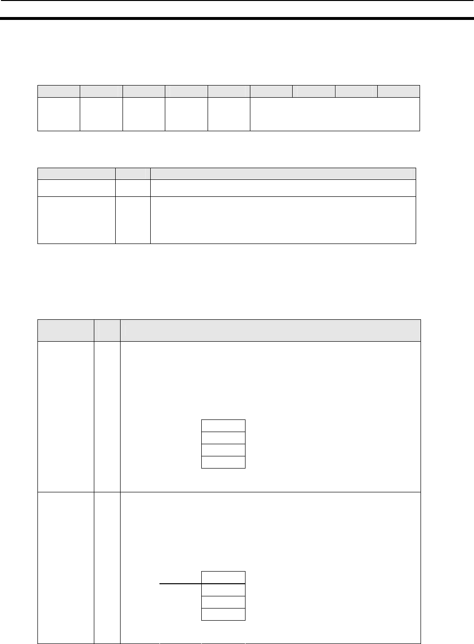
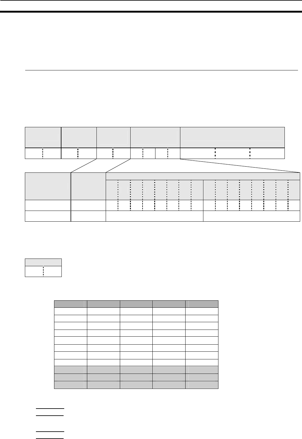
4) Communications Modes Diagrams
1) Single Trigger
Operation Sequence
2) Single Auto
Operation Sequence
3) Single Repeat
Operation Sequence
Host control unit to RIFD Unit
RIFD Unit to host control unit
Communications with ta
g
Ta
g
o
p
eration
command
command
response1 response2
tag 1
Command processing
No Tag Error
Command processing
command
command
response1 response
tag 1
Tag detection End processing
stop
Host control unit to RIFD Unit
RIFD Unit to host control unit
Communications with ta
g
Ta
g
o
p
eration
Command
processing Tag detection
command
response1 response3
tag 1
stop
tag 2
response2
tag 3
response
Host control unit to RIFD Unit
RIFD Unit to host control unit
Communications with ta
g
Ta
g
o
p
eration
Tag detection Tag detection
Tag
detection
Tag detection
Command
processing
Command
processing Command
processing
End processing
4-2 Data Formats
Section 4-2
4-8
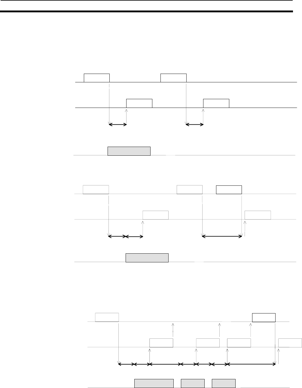
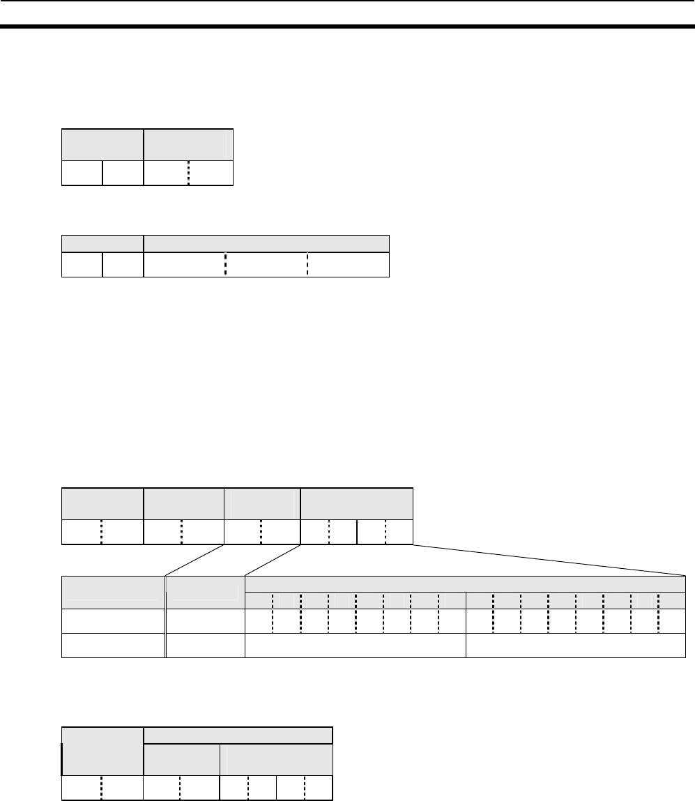
4) FIFO Trigger
Operation Sequence
5) FIFO Auto
Operation Sequence
6) FIFO Continuous
Operation Sequence
7) FIFO Repeat
Operation Sequence
command command
response1 response2
tag 1
No Tag Error
Unmodulated oscillation
Host control unit to RIFD Unit
RIFD Unit to host control unit
Communications with ta
g
Ta
g
operation
Command
processing Command
processing Unmodulated oscillation
command
command
response1 response
tag 1
Tag
detection
End processing
stop
Host control unit to
RFID Unit
RFID Unit to host control unit
Communications with tag
T
ag operation
Command
p
rocessin
g
Unmodulated
oscillation
Tag
detection
command
response1
tag 1
End processing
stop
tag 2
response2 response
ACK
response2
NACK
Host control unit to RIFD Unit
RIFD Unit to host control unit
Communications with ta
g
Ta
g
o
p
eration
Tag
detection
Tag
detection
Unmodulated
oscillation
Unmodulated oscillation
Command
processing
command
response1 response3
tag 1
stop
tag 2
response2
tag 3
response
Host control unit to RIFD Unit
RIFD Unit to host control unit
Communications with ta
g
T
a
g
operation
Tag
detection
Tag
detection Tag detection
Command
processing
Command
processing Command
processing
Tag
detection
End processing

4-2 Data Formats
Section 4-2
4-9
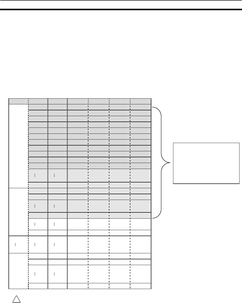
4-2-3 End Code List
Communications between Host Device and RFID Unit
End code Name Details
10 Parity Error • There is a character with a parity error in the command received.
11 Framing Error • There is a character with a framing error in the command received.
12 Overrun Error • There is a character with an overrun error in the command received.
14 Format Error
• Command format does not match specifications.
Examples: Command is not defined, page/address specifications are
invalid, etc.
18 Frame Error • Characters are received more than 2 sec apart
• Frame received exceeds 140
Communications between RFID Unit and Tags
End code Name Details
70 Communications Error • Interference, such as noise, has occurred during communications with
the tags, preventing normal completion.
71 Write Error
• Write command has been specified to a page that has been
write-prohibited.
• There is a tag area to which reading is possible, but writing is not possible.
• Correct data cannot be written because the tag has exceeded its
usable write life.
72 No Tag Error
• There was no tag in the communications area when the command
was executed.
• The specified pages do not exist (I-CODESLI).
79 Command Error • (see Comparison with ISO Error Code)
7A Address Error • The specified pages do not exist.
Comparison with ISO Error Code
When an ISO tag responds by returning an error, the unit responds with the end code shown in the
following table.
ISO code Details End code
01 Command not in use. Cannot recognize request command code. 79
02 Unrecognized command. Example: format error 79
03 Any unused command. 79
0F Unknown or unused error code. 79
10 Specified block cannot be used (not present). 7A
11 Specified block cannot be re-locked because it has been already locked. 00
12 The contents of the specified block cannot be changed because it is locked. 71
13 Writing to the specified block did not end normally. 71
14 Locking of the specified block did not end normally. 71
Others RFU 79
4-3 Commands and Responses during CR Control
Section 4-3
4-3 Commands and Responses during CR Control
4-3-1 General Commands (Commands sent to the RFID Unit)
1) Test
This command tests communications with the host. When this command is received, the RFID Unit
sends the same data to the host.
Command
Command Test data
‘ 1 ‘ ‘ 0 ‘ Data 1 ⋅⋅⋅⋅⋅⋅ Data n
Response
End code Test data
‘ 0 ‘ ‘ 0 ‘ Data 1 ⋅⋅⋅⋅⋅⋅ Data n
The test data returned is the same as the command data.
2) ACK
Use this command when the communications mode is FIFO Continuous Mode.
ACK is sent after the response has been received, and the next read operation is permitted.
Command
Command
‘ 1 ‘ ‘ 1 ‘
Response
There is no response to ACK.
3) NACK
If the host control unit does not receive a response normally, NACK is sent as a request to resend the
response.
When the RFID Unit receives the NACK command, it resends the immediately preceding response.
Command
Command
‘ 1 ‘ ‘ 2 ‘
Response
The immediately preceding response data is resent.
4) STOP
Use this command to stop the RFID Unit processing. When this command is received, the RFID Unit
stops processing the current command and enters sleep mode. If the antenna is oscillating, the oscilla-
tion also stops.
Command
Command
‘ 1 ‘ ‘ 3 ‘
Response
End code
‘ 0 ‘ ‘ 0 ‘
4-3 Commands and Responses during CR Control
Section 4-3
4-11
4-3-2 Commands Common to the I-CODE1 and the I-CODESLI Chips
1) Read
Use this command to read data from the tags. Data can be read from a user-specified page.
Command
This command sends the pages to be read as command parameters. The page specification is as follows: The
bits that correspond to the pages to be read are set to 1, and all other bits are set to 0. This binary number is
converted to hexadecimal and sent with the command. The pages are specified by the user.
Command Communi-
cations
option
Bank
specifica-
tion
Page specification
‘ 3‘ ‘ 1 ‘
Page specification (settable value)
Tag type Bank specifi-
cation
(Settable value) F E D C B A 9 8 7 6 5 4 3 2 1 0
I-CODE1 ‘ 00 ‘ ‘00’ to ‘FF’ ‘00’ to ‘FF’
ISO chip ‘00’ to ‘0F’ ‘00’ to ‘FF’ ‘00’ to ‘FF’
Response
Returns the data read and the end code (normal end: ‘00’). The read data is returned sequentially in
ascending order of the pages specified. If an error occurs, an error code is returned. In the case of a Tag
equipped with I-CODE1, the read data is returned in the order: B⇒C⇒D⇒E⇒F⇒0⇒1⇒···⇒A.
End code Read data
*1
‘ 0 ‘ ‘ 0 ‘ Data 1 ・・・ Data n
*1 Number of data n = Number of specified pages x 8 (hexadecimal)
Number of data n = Number of specified pages x 4 (ASCII)
Command Example
The following table gives the tag user memory details for the following example of commands and responses.
Page Byte 0 Byte 1 Byte 2 Byte 3
0 30 Hex 31 Hex 32 Hex 33 Hex
1 34 Hex 35 Hex 36 Hex 37 Hex
2 38 Hex 39 Hex 30 Hex 30 Hex
3 40 Hex 41 Hex 42 Hex 43 Hex
4 44 Hex 45 Hex 46 Hex 47 Hex
5 48 Hex 49 Hex 4A Hex 4B Hex
6 4C Hex 4D Hex 4E Hex 4F Hex
7 50 Hex 51 Hex 52 Hex 53 Hex
8 54 Hex 55 Hex 56 Hex 57 Hex
9 58 Hex 59 Hex 5A Hex 61 Hex
10 62 Hex 63 Hex 64 Hex 65 Hex
(1) Reading the following four pages: 1, 3, 5, and 6, using Single Trigger Mode with hexadecimal is as
follows:
Command ‘01 00 006A<CR>‘
Response ‘00 34353637 40414243 48494A4B 4C4D4E4F<CR>‘
(2) Reading the following four pages: 1, 3, 5, and 6, using Single Trigger Mode with ASCII is as follows:
Command ‘01 10 006A<CR>‘
Response ‘00 4567 @ABC HIJK LMNO<CR>‘
4-3 Commands and Responses during CR Control
Section 4-3
4-12
2) Write
Use this command to write tag data on a page basis. Data can be written to user-specified pages (except
B Hex to E Hex for I-CODE1). The maximum number of pages which can be written to in a single op-
eration is one bank, and writing to pages across banks is impossible. There is no need to perform the
verify read process, since this command performs it as part of its execution.
Command
This command sends the data to be written as parameters. The page specification is as follows: The bits
that correspond to the pages to be written are set to 1, and all other bits are set to 0. This binary number
is converted to hexadecimal and sent with the command. Specify the write data sequentially in as-
cending order of the specified page. In the case of a Tag equipped with I-CODE1, specify the write data
in the order: F⇒0⇒1⇒···⇒A.
Command Communi-
cations
option
Bank speci-
fication
Page specifica-
tion Write data
*1
‘ 3‘ ‘ 2 ‘ Data 1 … Data n
Page specification (settable value)
Tag type
Bank
specification
(Settable
value) F E D C B A 9 8 7 6 5 4 3 2 1 0
I-CODE1 ‘ 00 ‘ 0000
ISO chip ‘00’ to ‘0F’ ‘00’ to ‘FF’ ‘00’ to ‘FF’
*1 Number of data n = Number of specified pages x 8 (hexadecimal)
Number of data n = Number of specified pages x 4 (ASCII)
Response
The response returns the end code (normal end: ‘00’).
End code
‘ 0 ‘ ‘ 0 ‘
Command Example
The following table gives details of tag user memory when executing the following command.
Page Byte 0 Byte 1 Byte 2 Byte 3
0 30 Hex 31 Hex 32 Hex 33 Hex
1 34 Hex 35 Hex 36 Hex 37 Hex
2 38 Hex 39 Hex 30 Hex 30 Hex
3 40 Hex 41 Hex 42 Hex 43 Hex
4 44 Hex 45 Hex 46 Hex 47 Hex
5 48 Hex 49 Hex 4A Hex 4B Hex
6 4C Hex 4D Hex 4E Hex 4F Hex
7 50 Hex 51 Hex 52 Hex 53 Hex
8 52 Hex 46 Hex 49 Hex 44 Hex
9 58 Hex 59 Hex 5A Hex 61 Hex
10 56 Hex 37 Hex 32 Hex 30 Hex
(1) Writing 52464944 hexadecimal to page 8, and 56373230 hexadecimal to page 10 using FIFO
Repeat Mode, with hexadecimal:
Command ‘02 0B 0500 52464944 56373230<CR>‘
Response ‘00<CR>
(2) Writing ‘RFID’ hexadecimal to page 8, and ‘V720’ hexadecimal to page 10 using FIFO Repeat Mode,
with ASCII:
Command ‘02 1B 0500 RFID V720<CR>‘
Response ‘00<CR>‘
Data written to tag memory is the same for both (1) and (2).
4-3 Commands and Responses during CR Control
Section 4-3
4-13
3) Write identical data
Use this command to write identical data to tags by the page. Data can be written to user-specified pages (except B
Hex to E Hex for I-CODE1). This command is useful when writing the same data to multiple pages.
The maximum number of pages which can be written to in a single operation is one bank, and writing to
pages across banks is impossible.
There is no need to perform the verify read process, since this command performs it as part of its execution.
Command
As parameters, the command sends specification of the pages to be written and the data to write to the
specified pages one page at a time. The page specification is as follows: The bits that correspond to the
pages to be written are set to 1, and all other bits are set to 0. This binary number is converted to
hexadecimal and sent with the command. The write data is specified sequentially in ascending order of
the pages specified. In the case of a Tag equipped with I-CODE1, specify the write data in the order:
F⇒0⇒1⇒···⇒A.
Command Communi-
cations
option
Bank speci-
fication
Page specifica-
tion Write data
*1
‘ 3‘ ‘ 3 ‘ Data 1 … Data n
Page specification (settable value)
Tag type
Bank
specification
(Settable
value) F E D C B A 9 8 7 6 5 4 3 2 1 0
I-CODE1 ‘ 00 ‘ 0000
ISO chip ‘00’ to ‘0F’ ‘00’ to ‘FF’ ‘00’ to ‘FF’
*1 Number of data n = Number of specified pages x 8 (hexadecimal)
Number of data n = Number of specified pages x 4 (ASCII)
Response
The response returns the end code (normal end: ‘00’).
End code
‘ 0 ‘ ‘ 0 ‘
Command Example
The following table gives details of tag user memory when executing the following command.
Page Byte 0 Byte 1 Byte 2 Byte 3
0 30 Hex 31 Hex 32 Hex 33 Hex
1 34 Hex 35 Hex 36 Hex 37 Hex
2 38 Hex 39 Hex 30 Hex 30 Hex
3 40 Hex 41 Hex 42 Hex 43 Hex
4 44 Hex 45 Hex 46 Hex 47 Hex
5 48 Hex 49 Hex 4A Hex 4B Hex
6 4C Hex 4D Hex 4E Hex 4F Hex
7 50 Hex 51 Hex 52 Hex 53 Hex
8 30 Hex 30 Hex 30 Hex 30 Hex
9 30 Hex 30 Hex 30 Hex 30 Hex
10 30 Hex 30 Hex 30 Hex 30 Hex
(1) Writing 30303030 hexadecimal to pages 8, 9, and 10 using FIFO Trigger Mode with hexadecimal:
Command ‘03 08 0700 30303030<CR>‘
Response ‘00<CR>
(2) Writing ‘0000’ to pages 8, 9, and 10 using FIFO Trigger Mode with ASCII:
Command ‘03 18 0700 0000<CR>‘
Response ‘00<CR>
Data written to tag memory is the same for both (1) and (2).
4-3 Commands and Responses during CR Control
Section 4-3
4-14
4) Read UID (SNR)
Use this command to read the serial numbers from the tags.
Command
Command Communica-
tions option
‘3’ ‘5’
Response
The response returns the UID (SNR) read and the end code (normal end: 00).
End code UID (SNR)
‘ 0 ‘ ‘ 0 ‘ Data 1 ・・・ Data 8
5) Set write-protection to Tag
Use this command to write-prohibit tags.
The maximum number of pages that can be write-protected in a single operation is one bank, and
write-protecting pages across banks is impossible.
Command
This command sends the pages to be write-protected as command data. The page specification is
achieved by setting the bit corresponding to each page to ON. When performing reading only, all the
page specifications are set to OFF.
Command Communica-
tions option
Bank
specification
Page
specification
‘ 3 ‘ ‘ 9 ‘
Page specification (settable value)
Tag type Bank F E D C B A 9 8 7 6 5 4 3 2 1 0
I・CODE1 ‘00’ 00
ISO chip ‘00’ to ‘0F’ ‘00’ to ‘FF’ ‘00’ to ‘FF’
Response
The response returns the setting status for write-protection and the end code (normal end: '00').
Setting status
End code Bank
specification Page
specification
‘ 0 ‘ ‘ 0 ‘
4-3 Commands and Responses during CR Control
Section 4-3
4-15
4-3-3 Commands Specific to the I-CODESLI Chip
1) Write, Lock AFI
Use this command to change or lock tag AFI.
Command
Command Communica-
tions option Process
option Data
‘ 3 ‘ ‘ 6 ‘
Process
option Data
Write AFI 01 Hex AFI = 00 to FF(Hex)
Lock AFI 02 Hex 00 Hex
Response
The response returns the end code (normal end: ‘00’).
End code
‘ 0 ‘ ‘ 0 ‘
2) Write, Lock DSFID
Use this command to change or lock tag DSFID.
Command
Command Communica-
tions option Process
option Data
‘ 3 ‘ ‘ 7 ‘
Process
option Data
Write DSFID 01 Hex AFI = 00 to FF(Hex)
Lock DSFID 02 Hex 00 Hex
Response
The response returns the end code (normal end: ‘00’).
End code
‘ 0 ‘ ‘ 0 ‘
4-3 Commands and Responses during CR Control
Section 4-3
4-16
3) Read Tag Info
Use this command to read tag system information.
Command
Command Communica-
tions option
‘ 3 ’ ‘ A ’
Response
The response returns the information flag, UID, the information data, and the end code (normal end: '00').
The data returned in the information data is changed with the information flag.
End code Informa-
tion flag UID Information
‘ 0 ‘ ‘ 0 ‘ Data 1 ・・・ Data 8 Data 1 ・・・ Data n
・Information flag
Bit 7 6 5 43 2 1 0
0 0 0 0 IC infor-
mation
Memory size
AFI DSFID
・Information (variable data length)
VICC memory size
DSFID AFI Number of
blocks Block
length
IC informa-
tion
*Only information with the bit set by the information flag is stored.
*Number of blocks = 00h (1 block) to FFh (256 block)
*Block length = 00h (1 byte) to 1Fh (32 byte)
4) Read UID & Data
Use this command to read UID and data from the tags at the same time. Data can be read from a
user-specified page.
The maximum number of pages that can be read in one operation is one bank (16 pages), and reading
pages across banks is impossible.
Command
This command sends the pages to be read as command data. The page specification is achieved by
setting the bit corresponding to each page to ON.
Command Communi-
cations
option
Bank
specifica-
tion Page specification
‘ 4 ‘ ‘ 1 ‘
Page
Tag type Bank F E D C B A 9 8 7 6 5 4 3 2 1 0
ISO chip 00 to 0F
Response
The response returns the UID and data read and the end code (normal end: 00). The read data is re-
turned sequentially in the order of the pages specified.
End code UID Read data*
‘ 0 ‘ ‘ 0 ‘ Data 1 ・・・ Data 8 Data 1 ・・・ Data n
* Number of read data n = Number of specified pages × page unit (4 bytes)
4-3 Commands and Responses during CR Control
Section 4-3
4-17
5) EAS Alarm Command
Requests EAS data to the tags.
Command
Command Communica-
tions option
‘ 4 ‘ ‘ 2 ‘
Response
The response returns the EAS data read and the end code (normal end: 00).
End code EAS data
‘ 0 ‘ ‘ 0 ‘ ‘F4CD460EABE509FE178D011C4B81926E415B5961F6F5D10D8F398B48A54EECF7’
6) Set EAS
Enables/disables and locks EAS to the tags.
Command
Command Communica-
tions option Process
option Data
‘ 4 ‘ ‘ 3 ‘
Process
option Data
Enable EAS 01 HEX 00 HEX: disabled/01
HEX: enabled
Lock EAS 02 Hex 00 Hex
Response
The response returns the end code (normal end: ‘00’).
End code
‘ 0 ‘ ‘ 0 ‘
4-3 Commands and Responses during CR Control
Section 4-3
4-18
4-3-4 Commands Specific to the I-CODE1 Chip
1) Read Serial Nnumber
Use this command to read tag serial numbers.
Command
Command
‘ 0 ‘ ‘ 5 ‘
Response
The response returns the tag serial number read, and the end code (normal end: '00').
End code Tag serial number
‘ 0 ‘ ‘ 0 ‘ Data 1 …… Data n
The tag serial number is 16 digits in hexadecimal code.
2) Read Family Code and Application ID
Use this command to read tag family codes and application IDs.
Command
Command
‘ 0 ‘ ‘ 6 ‘
Response
The response returns the tag family code, application ID read, and end code (normal end: '00').
End code
Family Code
Application
ID
‘ 0 ‘ ‘ 0 ‘ ‘00’ to ‘FF’ ‘00’ to ‘FF’
3) Write Family Code and Application ID
Use this command to set the tag family codes and application IDs.
Command
Command
Family Code
Application
ID
‘ 0 ‘ ‘ 7 ‘ ‘00’ to ‘FF’ ‘00’ to ‘FF’
Response
The response returns the end code (normal end: ‘00’).
End code
‘ 0 ‘ ‘ 0 ‘
4-3 Commands and Responses during CR Control
Section 4-3
4-19
4) Set EAS mode
Use this command to set whether to permit or prohibit tag EAS responses.
Command
Command Set value
‘ 0 ‘ ‘ 8 ‘
Set value: ’ 00 ‘ Permit
’ 01 ‘ Prohibit
Response
The response returns the end code (normal end: ‘00’).
End code
‘ 0 ‘ ‘ 0 ‘
5) EAS
Sends EAS commands to the tags. EAS data, which is the response from the tags, is fixed data, as
shown below.
Command
Command
‘ 2 ‘ ‘ 4 ‘
Response
EAS data
‘ 2FB36270D5A7907FE8B18038D281497682DA9A866FAF8BB0F19CD112A57237EF ‘
Note If there is no tag in the communications area, undefined data of 64 characters will be returned.
4-3 Commands and Responses during CR Control
Section 4-3
4-20
4-3-5 Old Commands Specific to the I-CODE1 Chip
The command can be replaced by Section 4 “
Commands Common to the I-CODE1 and the I-CODESLI Chips
”.
1) Read
Use this command to read data from the tags. Data can be read from a user-specified page.
Command
This command sends the pages to be read as command parameters. The page specification is as fol-
lows: The bits that correspond to the pages to be read are set to 1, and all other bits are set to 0. This
binary number is converted to hexadecimal and sent with the command. The pages are specified by the
user.
Command Communica-
tions option Page specification
(4 characters)
‘ 0 ‘ ‘ 1‘
Bit 7 6 5 4 3 2 1 0 7 6 5 4 3 2 1 0
Page F E D C B A 9 876543210
Settable
Value ‘00’ to ‘FF’ ‘00’ to ‘FF’
Response
The response returns the data read and the end code (normal end: ‘00’).The read data is returned
sequentially in ascending order of the pages specified. If an error occurs, an error code is returned.In the
case of a Tag equipped with I-CODE1, the read data is returned in the order:
B⇒C⇒D⇒E⇒F⇒0⇒1⇒···⇒A.
End code Read data
*1
‘ 0 ‘ ‘ 0 ‘ Data 1 ⋅⋅⋅⋅⋅⋅ Data n
*1 Number of data n = Number of specified pages x 8 (hexadecimal)
Number of data n = Number of specified pages x 4 (ASCII)
<Command Example>
The following table gives the tag user memory details for the following example of commands and re-
sponses.
Page Byte 0 Byte 1 Byte 2 Byte 3
0 30 Hex 31 Hex 32 Hex 33 Hex
1 34 Hex 35 Hex 36 Hex 37 Hex
2 38 Hex 39 Hex 30 Hex 30 Hex
3 40 Hex 41 Hex 42 Hex 43 Hex
4 44 Hex 45 Hex 46 Hex 47 Hex
5 48 Hex 49 Hex 4A Hex 4B Hex
6 4C Hex 4D Hex 4E Hex 4F Hex
7 50 Hex 51 Hex 52 Hex 53 Hex
8 54 Hex 55 Hex 56 Hex 57 Hex
9 58 Hex 59 Hex 5A Hex 61 Hex
10 62 Hex 63 Hex 64 Hex 65 Hex
(1) Reading the following four pages: 1, 3, 5, and 6, using Single Trigger Mode with hexadecimal is as follows:
Command ‘01 00 006A<CR>‘
Response ‘00 34353637 40414243 48494A4B 4C4D4E4F<CR>‘
(2) Reading the following four pages: 1, 3, 5, and 6, using Single Trigger Mode with ASCII is as follows:
Command ‘01 10 006A<CR>‘
Response ‘00 4567 @ABC HIJK LMNO<CR>‘
4-3 Commands and Responses during CR Control
Section 4-3
4-21
2) Write
Use this command to write data to tags on a page basis. Data is written to user-specified pages.
There is no need to perform the verify read process, since this command performs it as part of its
execution.
Command
This command sends the data to be written as parameters. The page specification is as follows: The bits
that correspond to the pages to be written are set to 1, and all other bits are set to 0. This binary number
is converted to hexadecimal and sent with the command. Specify the write data sequentially in as-
cending order of the pages specified. In the case of a Tag equipped with I-CODE1, specify the write data
in the order: F⇒0⇒1⇒···⇒A.
Command Communica-
tions option Page specification
(4 characters) Write data*1
‘ 0 ‘ ‘ 2 ‘ Data 1 ⋅⋅⋅⋅⋅⋅ Data n
Bit 7 65 4 3 2 1076543210
Page F E D C B A 9876543210
Settable
Value ‘ 00’ to ‘ 07 ‘
‘ 10’ to ‘ 17 ‘ ‘00’ to ‘FF’
*1 Number of data n = Number of specified pages x 8 (hexadecimal)
Number of data n = Number of specified pages x 4 (ASCII)
Response
The response returns the end code (normal end: ‘00’).
End code
‘ 0 ‘ ‘ 0 ‘
<Command Example>
The following table gives details of tag user memory when executing the following command.
Page Byte 0 Byte 1 Byte 2 Byte 3
0 30 Hex 31 Hex 32 Hex 33 Hex
1 34 Hex 35 Hex 36 Hex 37 Hex
2 38 Hex 39 Hex 30 Hex 30 Hex
3 40 Hex 41 Hex 42 Hex 43 Hex
4 44 Hex 45 Hex 46 Hex 47 Hex
5 48 Hex 49 Hex 4A Hex 4B Hex
6 4C Hex 4D Hex 4E Hex 4F Hex
7 50 Hex 51 Hex 52 Hex 53 Hex
8 52 Hex 46 Hex 49 Hex 44 Hex
9 58 Hex 59 Hex 5A Hex 61 Hex
10 56 Hex 37 Hex 32 Hex 30 Hex
(1) Writing 52464944 hexadecimal to page 8, and 56373230 hexadecimal to page 10 using FIFO
Repeat Mode, with hexadecimal:
Command ‘02 0B 0500 52464944 56373230<CR>‘
Response ‘00<CR>
(2) Writing ‘RFID’ hexadecimal to page 8, and ‘V720’ hexadecimal to page 10 using FIFO Repeat Mode,
with ASCII:
Command ‘02 1B 0500 RFID V720<CR>‘
Response ‘00<CR>‘
Data written to tag memory is the same for both (1) and (2).
4-3 Commands and Responses during CR Control
Section 4-3
4-22
3) Write identical data
Use this command to write identical data to tags by the page. Data is written to user-specified pages.
This command is useful when writing the same data to multiple pages (specification is required only
once).
There is no need to perform the verify read process, since this command performs it as part of its
execution.
Command
As parameters, the command sends specification of the pages to be written and the data to write to the
specified pages one page at a time. The page specification is as follows: The bits that correspond to the
pages to be written are set to 1, and all other bits are set to 0. This binary number is converted to
hexadecimal and sent with the command. Specify the write data sequentially in ascending order of the
pages specified. In the case of a Tag equipped with I-CODE1, specify the write data in the order:
F⇒0⇒1⇒···⇒A.
Command Communica-
tions option Page specification
(4 characters) Write data*1
‘ 0 ‘ ‘ 3‘ Data 1 ⋅⋅⋅⋅⋅⋅ Data n
Bit 7 6 5 4 3 2 1 0 7 6 5 4 3 2 1 0
Page F E D C B A 9 876543210
Settable
Value ‘ 00’ to ‘ 07 ‘
‘ 10’ to ‘ 17 ‘ ‘00’ to ‘FF’
*1 Number of data n = Number of specified pages x 8 (hexadecimal)
Number of data n = Number of specified pages x 4 (ASCII)
Response
The response returns the end code (normal end: ‘00’).
End code
‘ 0 ‘ ‘ 0 ‘
Command Example
The following table gives details of tag user memory when executing the following command.
Page Byte 0 Byte 1 Byte 2 Byte 3
0 30 Hex 31 Hex 32 Hex 33 Hex
1 34 Hex 35 Hex 36 Hex 37 Hex
2 38 Hex 39 Hex 30 Hex 30 Hex
3 40 Hex 41 Hex 42 Hex 43 Hex
4 44 Hex 45 Hex 46 Hex 47 Hex
5 48 Hex 49 Hex 4A Hex 4B Hex
6 4C Hex 4D Hex 4E Hex 4F Hex
7 50 Hex 51 Hex 52 Hex 53 Hex
8 30 Hex 30 Hex 30 Hex 30 Hex
9 30 Hex 30 Hex 30 Hex 30 Hex
10 30 Hex 30 Hex 30 Hex 30 Hex
(1) Writing 30303030 hexadecimal to pages 8, 9, and 10 using FIFO Trigger Mode with hexadecimal:
Command ‘03 08 0700 30303030<CR>‘
Response ‘00<CR>
4-3 Commands and Responses during CR Control
Section 4-3
4-23
(2) Writing ‘0000’ to pages 8, 9, and 10 using FIFO Trigger Mode with ASCII:
Command ‘03 18 0700 0000<CR>‘
Response ‘00<CR>
Data written to tag memory is the same for both (1) and (2).
4) Set lock
Use this command to write-prohibit tags.
Command
This command sends the pages to be write-protected as command data. The page specification is as
follows: The bits that correspond to the pages to be write-protected are set to 1, and all other bits are set
to 0. This binary number is converted to hexadecimal and sent with the command. To read the current
write-prohibit settings, set the page specification to '0000'.
Command Page specification
(4 characters)
‘ 0 ‘ ‘ 9 ‘
Bit 7 65 4 3 2 1076543210
Page F E D C B A 9876543210
Settable
Value Page B Hex and C Hex
must be 0. ‘00’ to ‘FF’
Response
The response returns the setting status for write-protection and the end code (normal end: '00'). The
page specification is as follows: The bits that correspond to the write-protect pages are set to 1, and all
other bits are set to 0.
End code Setting status
‘ 0 ‘ ‘ 0 ‘
Bit 7 65 4 3 2 1076543210
Page F E D C B A 9876543210
Value Page B Hex and C Hex
are 0. ‘00’ to ‘FF’
Note The lock function used with the V720 Series cannot be canceled. Pages that have been
write-protected cannot be written to again, so be careful when using this function.
5-1
SECTION 5
Characteristics Data (Reference)
5-1 Communications Distance (Reference)................................................................5-2
5-2 Diagram of Communications Range (Reference)................................................5-3
5-3 Communications Time (Reference) ......................................................................5-7
5-3-1 Communications time ............................................................................................5-7
5-3-2 TAT (Turn Around Time) ........................................................................................5-8
5-4 Effects of Surrounding Metal (Reference)............................................................5-9
5-5 Mutual Interference (Reference)............................................................................5-10
5-6 Positional Relation Between Rreader and Computer (Reference) ....................5-11

5-1 Communications Distance (Reference) Section 5-1
5-2
5-1 Communications Distance (Reference)
The communications distance is given in the following table. The communications distance changes,
however, depending on the tag inlet forming material, and the tag and RFID Unit mounting conditions,
so check the conditions of use beforehand.
1) I-CODE1 Tag Inlet
Model Specifications Shape Communication distance
(reference)
V720-D52P03 Inlet φ21 2 to 19mm
V720-D52P04 Inlet Rectangle
16.5x22 3 to 19mm
2) I-CODESLI Tag Inlet and Tag (available soon)
Model Specifications Shape Communication distance
(reference)
V720S-D13P01 Inlet ISO card
46 x 76 0 to 45 mm
V720S-D13P02 Inlet Half
46 x 43 0 to 36 mm
V720S-D13P06 Inlet 32 x 72 0 to 35 mm
V720S-D13P30 Tag ISO card
46 x 76 0 to 62 mm
V720S-D13P40 Tag ISO card
46 x 76 0 to 42 mm
Note The communications distances shown above are based on the use of standard tags at a
temperature of 25°C.
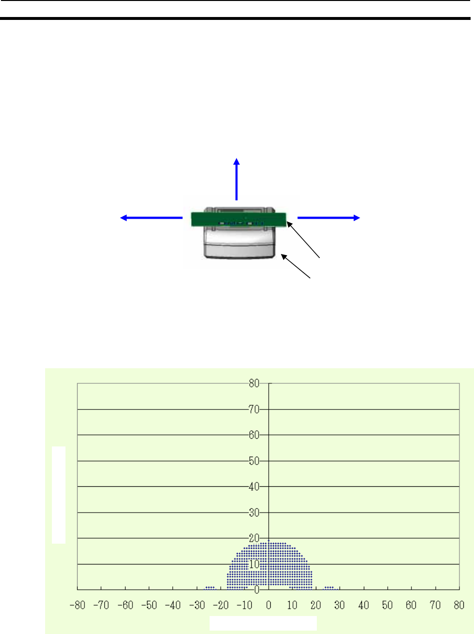
5-2 Diagram of Communications Range (Reference)
Section 5-2
5-3
5-2 Diagram of Communications Range (Reference)
A diagram of the V720S-HMU01 communications range is given below. The communications range
differs, however, depending on the mounting conditions and the environmental conditions.
X and Y directions represented in the following diagrams correspond to each direction of X and Y
directions shown with arrows in the following figure.
1) I-CODE1 Tag
タグ:
V 720-D 52P01
0
10
20
30
40
50
60
70
80
-80-70-60-50-40-30-20-10 0 1020304050607080
x
方向(mm)
y方向(mm
)
25℃
50℃
0℃
X direction (mm)
Y direction (mm)
X direction
(Positive)
X direction
(Negative)
Tag
Read/Write unit
Tag: V720-D52P03
Y direction
(Gaining the distance from the RFID unit)
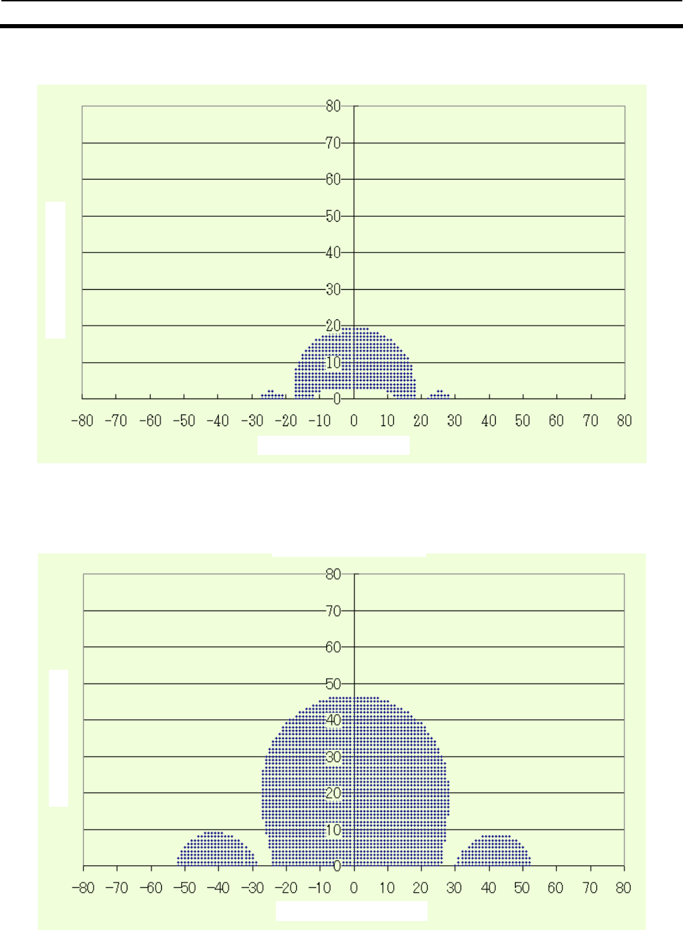
5-2 Diagram of Communications Range (Reference)
Section 5-2
5-4
2) I-CODESLI Tag
Tag: V720-D52P04
X direction (mm)
Y direction (mm)
Tag:
V720S
-
D13P01
X direction (mm)
Y direction (mm)
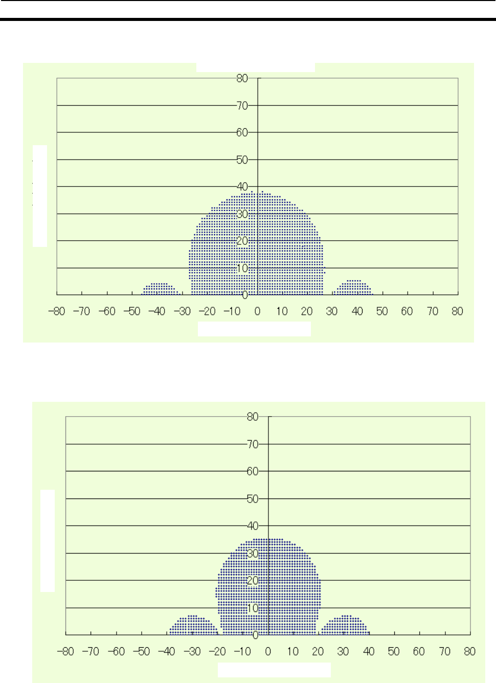
5-2 Diagram of Communications Range (Reference)
Section 5-2
5-5
Ta
g
: V720S-D13P02
X direction (mm)
Y direction (mm)
Tag: V720S-D13P06
X direction (mm)
Y direction (mm)
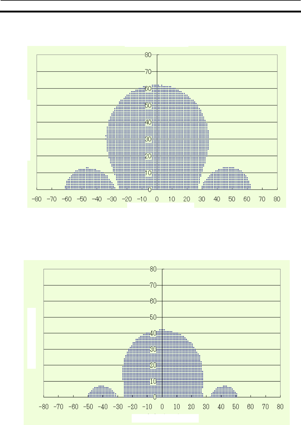
5-2 Diagram of Communications Range (Reference)
Section 5-2
5-6
Tag: V720S-D13P30
X direction (mm)
Y direction (mm)
Tag: V720S-D13P40
X direction (mm)
Y direction (mm)
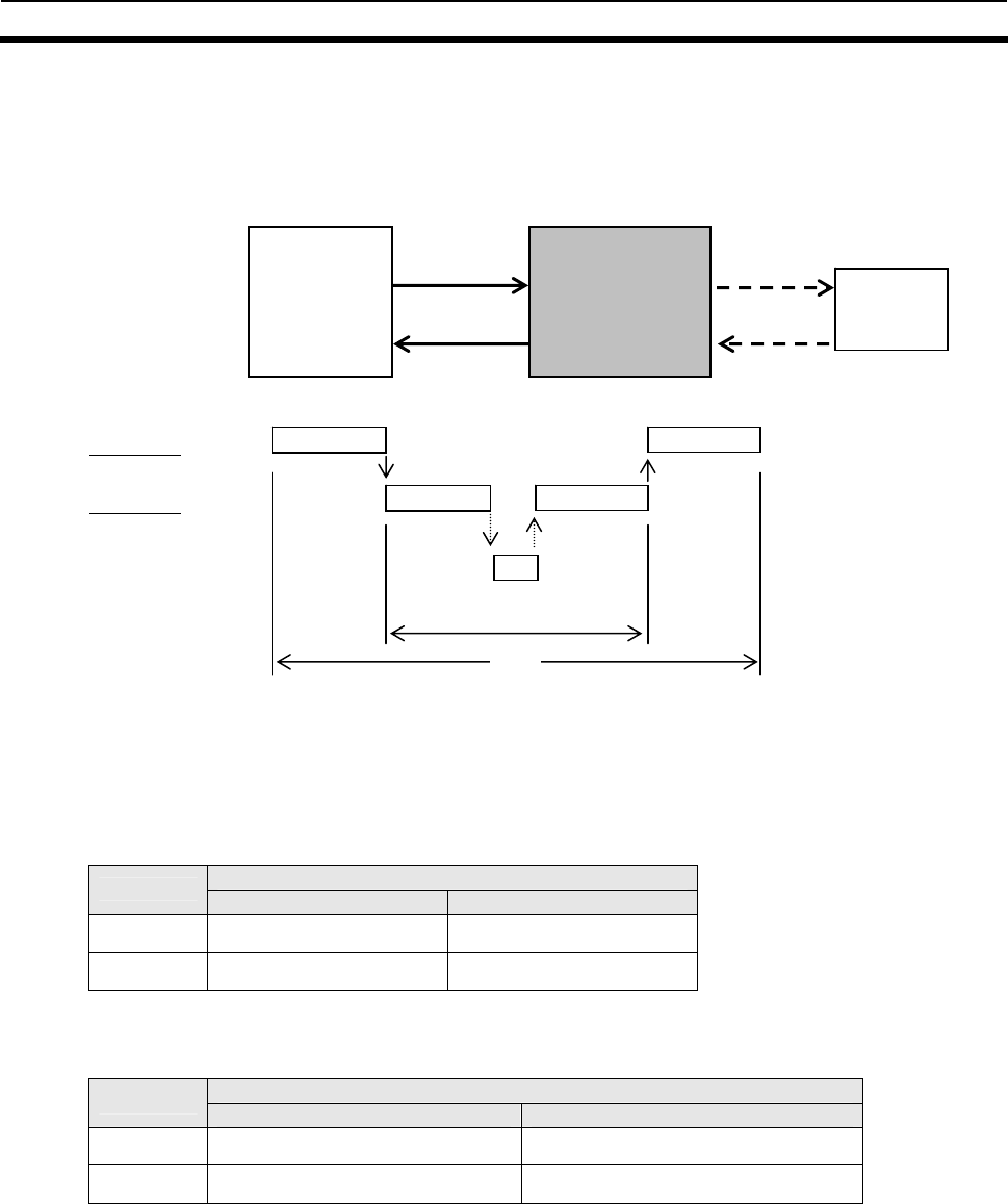
5-3 Communications TIme (Reference)
Section 5-3
5-7
5-3 Communications Time (Reference)
The communications time given below includes the communications time and TAT (Turn Around Time).
Computer
RFID Unit
5-3-1 Communications time
The communications time is the communications processing time between the RFID Unit and the tags.
The communications time differs depending on the number of pages being written or read.
Specifying Number of Pages to Be Written/Read Continuously
Formulas
Communications time (ms)
Command I-CODE 1 I-CODE SLI
Read T = 1.3N + 6.2 T = 1.3N + 6.0
Write T = 13N + 13.5 T = 13.6N + 15.5
N: No. of pages processed
Not Specifying Number of Pages to Be Written/Read Continuously
Formulas
Communications time (ms)
Command I-CODE1 I-CODESLI
Read T = 1.3N
R
+ 6.2 T = 1.3N
R
+6.0
Write T = 11.7N
W
+ 1.3N
R
+ 13.5 T = 12.3N
W
+ 1.3N
R
+ 15.5
NR = (Maximum number of specified pages – minimum number of specified pages) + 1
NW = No. of pages written
Note When using I-CODE1 tags, convert the pages Bh through Fh in the system area as shown
below:
Page B ⇒ Page -5
Page C ⇒ Page -4
Page D ⇒ Page -3
Page E ⇒ Page -2
Page F ⇒ Page -1
When using I-CODESLI tags, calculate the page numbers by converting them into decimal
numbers.
Command 1
Response 1
Computer
RFID Unit
V720S-HMU01
V720 series
Tag
Command 2
Response 2
Command 1 Response 1
Command 2 Response 2
Tag
Communications Time
TAT

5-3 Communications Time (Reference)
Section 5-3
5-8
Example: Reading data from pages 1, 5, and 9
T = 1.3 × ( 9 - 1 + 1 ) + 6.2 = 17.9 ms (for I-CODE1)
T = 1.3 × (9 - 1 + 1 ) + 6.0 = 17.7 ms (for I-CODESLI)
Example: Reading data from pages C, 5, and 9
T = 1.3 × (9-(-4)+1) + 6.2 = 24.4ms (for I-CODE1)
T = 1.3 × (12-5+1) + 6.0 = 16.6ms (for I-CODESLI)
Example: Writing data to pages 2, 4, 9, and 10
T = 11.7 × 4 + 1.3 × ( 10 - 2 + 1 ) + 13.5 = 72ms (for I-CODE1)
T = 12.3 × 4 + 1.3 × ( 10 - 2 + 1 ) + 15.5 = 76.4ms (for I-CODESLI)
Communications Time Calculation Conditions
•
Communications mode: Single Trigger Mode
•
Communications errors must not occur, such as due to noises.
5-3-2 TAT (Turn Around Time)
The TAT is the time taken from when the host control unit sends a command to the RFID Unit, to when
a response is received and completed.
The time differs depending on the baud rate and the communications control method setting.
Example of TAT Calculation
Example: Reading from page 0 to page 4
I-CODE1 I-CODESLI
(1)During command send
9[char.] × 11 [bits] / 9600[bps] × 1000[ms/s] ≈ 10.32ms
(2)During communications
6.5 + 6.2 = 12.7ms
(3)During reception of response
43[char.] × 11 [bits] / 9600[bps] × 1000[ms/s] ≈ 49.27ms
The TAT in to the above example is (1) + (2) + (3) = 72.29
ms.
(1)During command send
11[char.] × 11 [bits] / 9600[bps] × 1000[ms/s] ≈ 12.61ms
(2)During communications
6.5 + 6.0 = 12.5ms
(3)During reception of response
43[char.] × 11 [bits] / 9600[bps] × 1000[ms/s] ≈ 49.27ms
The TAT in to the above example is (1) + (2) + (3) = 74.38
ms.
The calculations are performed according to the following conditions.
•
Communications mode : Single Trigger Mode
•
Communications control method : CR control
•
Baud rate : 9,600 bps
•
Data code specification : Hexadecimal
•
Commands sent from the host control unit are sent continuously without spaces between the
characters.
•
Communications errors must not occur, such as due to noises.
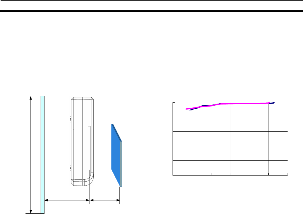
5-4 Effects of Surrounding Metal (Reference)
Section 5-4
5-9
5-4 Effects of Surrounding Metal (Reference)
If there is a metal backing plate on the RFID Unit, communication distance with the tags will be
reduced. The data given below is for aluminum and iron.
V720S-HMU01
Measuring conditions
Aluminum: 300 × 300 × t1.5 mm
Iron: 300 × 300 × t1.0 mm
Note Communication distance with tags may be reduced due to metallic materials used in the
operating environment such as a table or desk. The effect varies depending on the material.
Make sure how the material has impact on it before operation.
0
20
40
60
80
100
0 20406080100120
Distance from metal backing plate (mm)
Communications distance
reduction (%)
Iron
Aluminum
30
0
m
m
X Y
Metal
plate
Tag
X: distance between Metal and plate
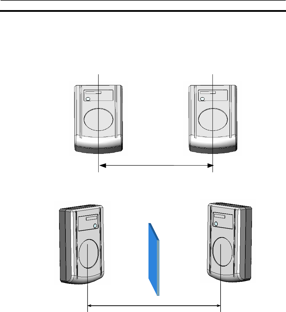
5-5 Mutual Interference (Reference)
Section 5-5
5-10
5-5 Mutual Interference (Reference)
If using multiple RFID Units near each other, keep a distance as shown below to prevent malfunction
due to mutual interference.
Parallel Antennas
Facing Antennas
Note Mutual interference depends on the operating environment of the RFID Unit and tags, so be
sure to check the environment before operation.
250 mm or more
100 mm or more
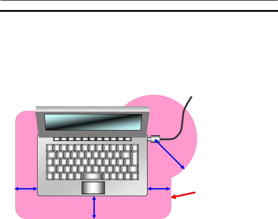
5-6 Positional Relation Between Reader and Comp
u
(R f )
Section 5-6
5-11
5-6 Positional Relation Between Reader and Computer
(Reference)
To minimize the effect of noise caused by computer (or the power supply circuit), keep the RFID unit
away from the area described as below.
When you use the reader with desktop computer, keep it away from the joint of AC power supply cord.
Note Effects of noise depend on the operating environment of the RFID Unit and the computer, so
be sure to check the environment before operation.
50mm or more
50mm or more
The radius of 150mm or
more of the DC jack for
external AC adaptor.
50mm or more
Keep the RFID unit away from
this area.
6-1
Section 6
Driver Installation
6-1 Before Installation ...............................................................................................6-1
6-2 Driver Installation .................................................................................................6-2

6-1 Before Installation 6-1
6-2
6-1 Before Installation
This section describes how to install the specified device driver (called “Driver”), which has to be
installed in the computer to operate the RFID unit (V720S-HMU01). This Driver appears as a virtual
COM port on the computer.
[System Requirements]
Make sure the computer to be connected with the RFID unit meets the system requirements for
running the Driver as below.
●OS: Windows XP home/Professional or Windows 2000 Professional.
●USB port available (USB1.0 or USB2.0)
●The specified Driver installable.
●An administrator of the computer shall install the Driver.
[How to obtain the Driver]
Visit our Web site (http://www.omronrfid.com/) and download the Driver from the download page.
If you download the Driver, the compressed file of V720S-HMU01.exe is stored in the computer.
Note:
- The Driver must be installed before connecting the RFID unit to your computer.
- If you happen to connect the RFID unit to the computer before installation of the Driver, cancel
the connection then start to install referring to “If you connect before installing” described in
the end of this section.
- An administrator of the computer shall install the Driver.
6-2 Driver Installation
[Decompression of the Driver]
(1) Run the V720S-HMU01(E).exe downloaded from the Web site mentioned above.
(2) The following dialog appears.
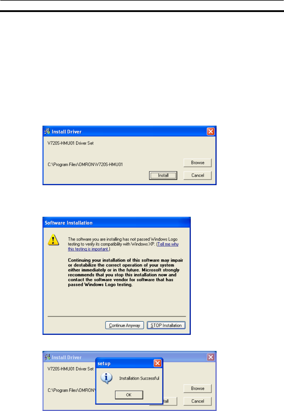
6-2 Driver Installation 6-2
6-3
(3) If you change the direction of the decompressed file, click “Change” then click “OK”.
If you do not change the direction, just click “OK”.
(4) The folder V720S-HMU01 appears in the directed folder.
If you do not change the direction, the folder V720S-HMU01 appears in the same folder as
V720S-HMU01.exe is placed.
V720S-HMU01 folder includes following two folders,
driver <= In this folder, the Driver is stored.
utility <= Utilities to be used for identification of port numbers are stored.
[Driver Installation]
(1) Double click the setup.exe in the driver folder to start the installation process.
(2) When the Install Driver dialog appears, click “Install”.
z If you use Windows XP SP2 or later version, the following page appears. On this page, click
“Continue” to go back to the Install Driver page. This warning page appears twice. On
each page, click “Continue”.
z If you use Windows 2000, this page does not appear.
(3) Install Driver page appears again and installation is processed.
Then, on the setup page, click OK to complete the install process.
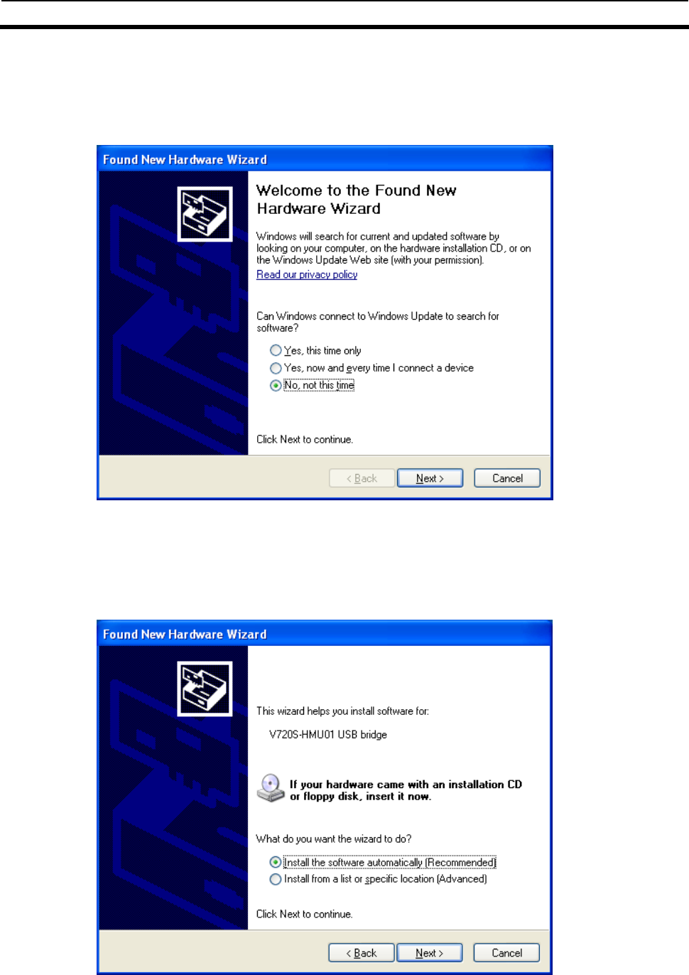
6-2 Driver Installation 6-2
6-4
[Connection with RFID Unit]
After installing the Driver, connect the RFID unit (V720S-HMU01) to the computer through USB
connector.
(1) Just after connecting the RFID unit to the computer, following page appears.
(2) On the “Found New Hardware Wizard” page, Click “No, not this time” and then click “Next”.
If you use the Windows 2000, this page is automatically skipped and the following page appears.
(3) On the second “Found New Hardware Wizard” page, make sure “Install the software
automatically [Recommended]” is checked then click the “Next” button.
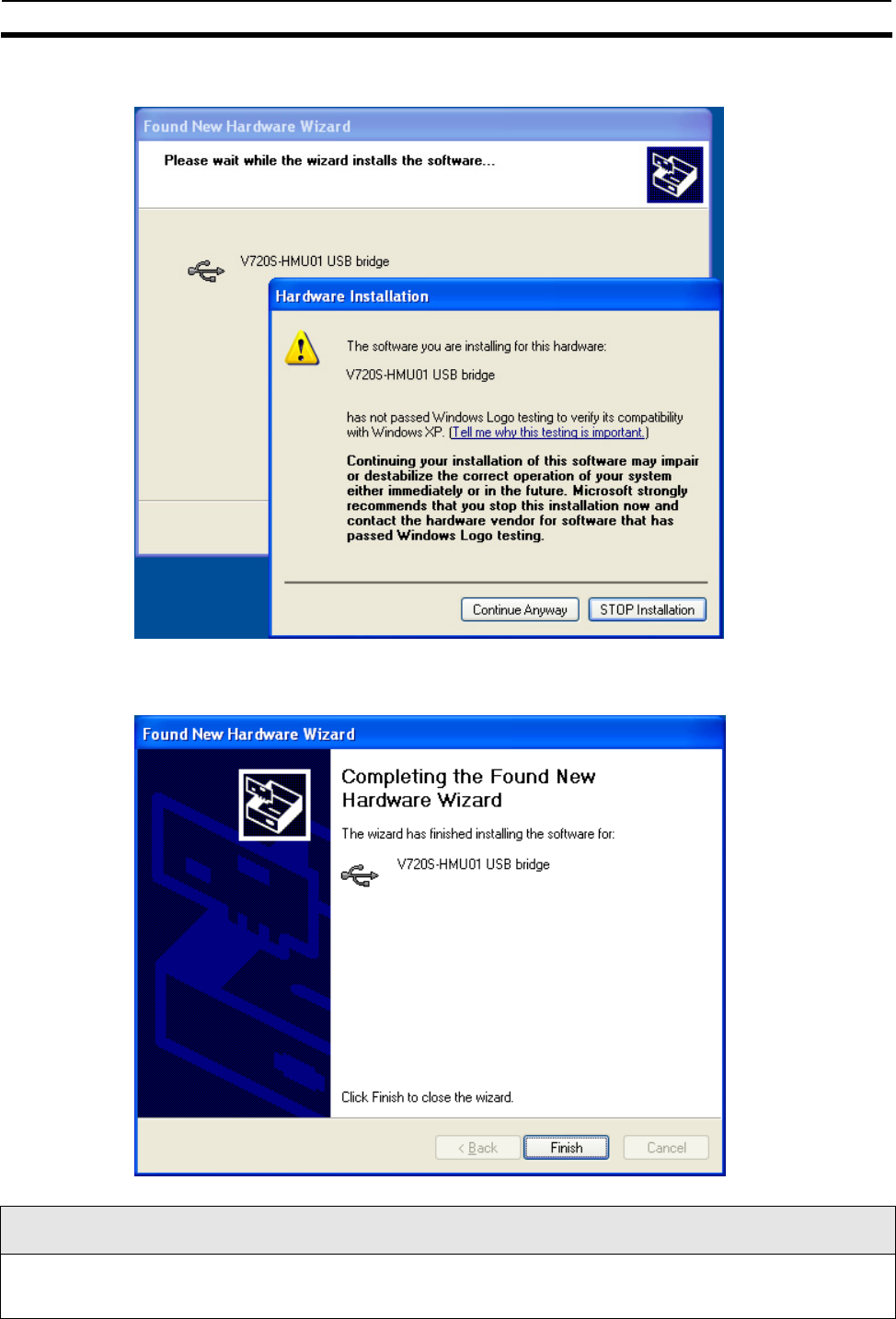
6-2 Driver Installation 6-2
6-5
(4) When the “Hardware Installation” page appears over the third “Found New Hardware Wizard”
page, click the “Continue” button.
(5) On the last “Found New Hardware Wizard” page, click “Finish” button to complete the wizard.
Now you are able to use the RFID unit.
Caution
● Above pages shown from (1) to (5) appear twice because two software; USB Bridge software and Virtual
COM software, have to be installed. In each time, implement in the same way according to the above
procedures.
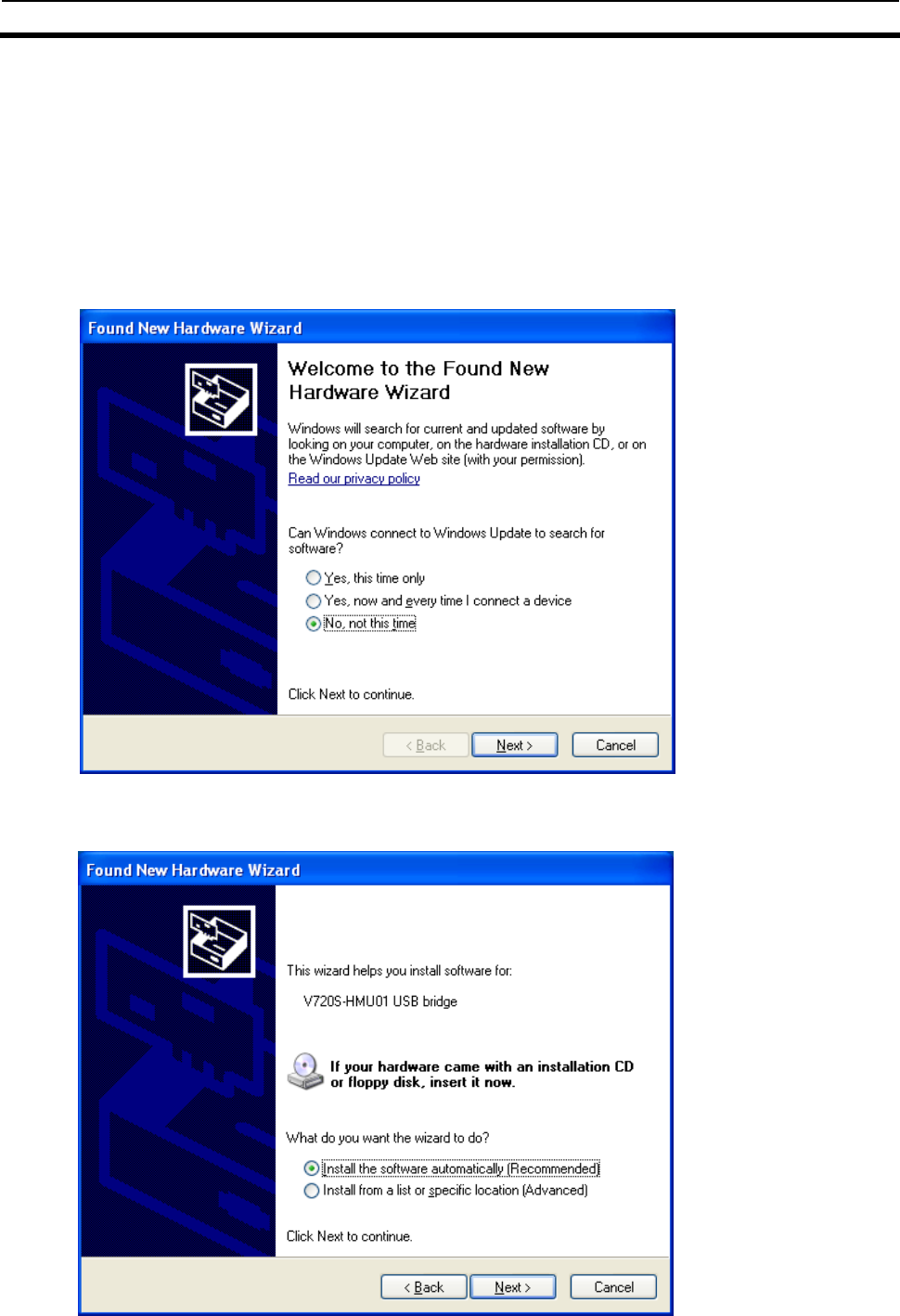
6-2 Driver Installation 6-2
6-6
[If you connect RFID unit before installing the Driver]
If you connect the RFID unit to the computer before installing the Driver, you can not set up the
Driver in the usual manner. After connecting the unit to the computer, one of following pages will
appear. See which page appears on your computer window and follow the procedures
corresponding to the page.
(1) On the page as below, click the “Cancel” button and then remove the RFID unit. Start Driver
installation according to the procedures described at the beginning of this section.
(2) On the page as below, click the “Cancel” button and then remove the RFID unit. Start Driver
installation according to the procedures described at the beginning of this section.
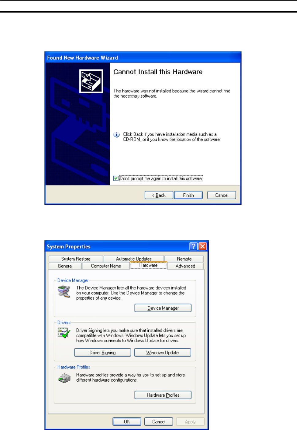
6-2 Driver Installation 6-2
6-7
(3) On the page as below, click the “Cancel” button and then remove the RFID unit. Start Driver
installation according to the procedures described at the beginning of this section. If you have
clicked the “Finish” on the page below, go to (4).
(4) If you happen to click the “Finish” button, you have to delete the device.
To delete the device, open the System Property window then click Hardware tab.
On the Hardware page, click “Device Manager”.
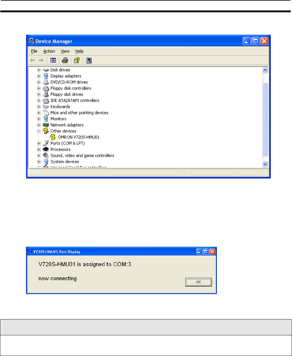
6-2 Driver Installation 6-2
6-8
(5) On the Device Manager page, make sure OMRON V720S-HMU01 appears under the “Other
Device”.
(6) Point the OMRON V720S-HMU01 and click the right mouse button to open drop-down menu.
Choose the “Delete” in the menu to complete deletion.
After deleting the device, remove the RFID unit, then start to install the Driver again.
[To See Port Number]
Find the disPort.exe file in the utility folder that is extracted from the driver file, V720S-HMU01.exe.
Click the disPort.exe file. Following dialogue appears.
You can check what port number is assigned for the RFID unit (In the case of above dialogue, COM3:
is assigned.)
Caution
● Execution of
dispPort.exe requires another file CP210xManufacturing.dll in the same folder.
If you copy or move the dispPort.exe to use it, copy or move the CP210xManufacturing.dll file into the same place.

Revision History
A manual revision code appears as a suffix to the manual number on the front cover of the manual.
Manual No. SRFM-017A
Revision code
The following table outlines the changes made to the manual during each revision. Page numbers refer to the
previous version.
Revision code Date Revised content
A Dec, 2007 The first edition

Manual No. SRFM017A
Note: Specifications subject to change without notice. Printed in Japan
Authorized Distributor:
Up-to-date information on RFID Systems can be accessed at OMRON's web site at
http://www.omronrfid.com/
OMRON CORPORATION
RFID BUSINESS DEVELOPMENT DEPARTMENT
3-4-10 Toranomon Minato-ku, Tokyo, 105-0001
Japan
Tel: (81)3-3436-7317/ Fax: (81)3-3436-7387
Regional Headquarters
OMRON ELECTRONICS LLC
RFID DIVISION
One Commerce Drive, Schaumburg, IL 60173
U.S.A.
Tel: (1)888-303-RFID (7343) /Fax: (1)847-925-1260
OMRON EUROPE B.V.
Wegalaan 57, NL-2132 JD Hoofddorp
The Netherlands
Tel: (31)23-568-1200/Fax: (31)23-568-1222
OMRON ASIA PACIFIC PTE. LTD.
83 Clemenceau Avenue,
#11-01, UE Square,
239920 Singapore
Tel: (65)835-3011/Fax: (65)835-2711
OMCC: OMRON (CHINA) CO., LTD.
Rm.302, AZIA Center, 1233 Lujiazui Ring Road
Pudong New Area, Shanghai 200120, PRC.
Tel: (86)21-5888-1666
Fax: (86)21-58888-7633/7933