Panasonic Devices Europe EBMU Bluetooth Module User Manual PAN1320 BT2 1 PO
Panasonic Industrial Devices Europe GmbH Bluetooth Module PAN1320 BT2 1 PO
UserManual.wiki
>
Panasonic Devices Europe
>
EBMU User Manual
>
15_PAN1320 UserMan_Rev1.2
Contents
1.
UserMan
2.
15_PAN1320 UserMan_Rev1.2
15_PAN1320 UserMan_Rev1.2
Navigation menu
Upload a User Manual
Namespaces
Wiki Guide
HTML
PDF
Info
Views
User Manual
Discussion / Help
Navigation
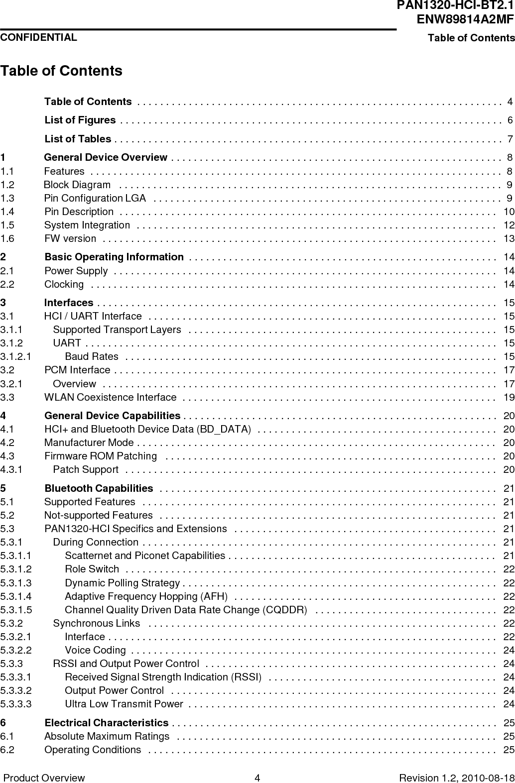
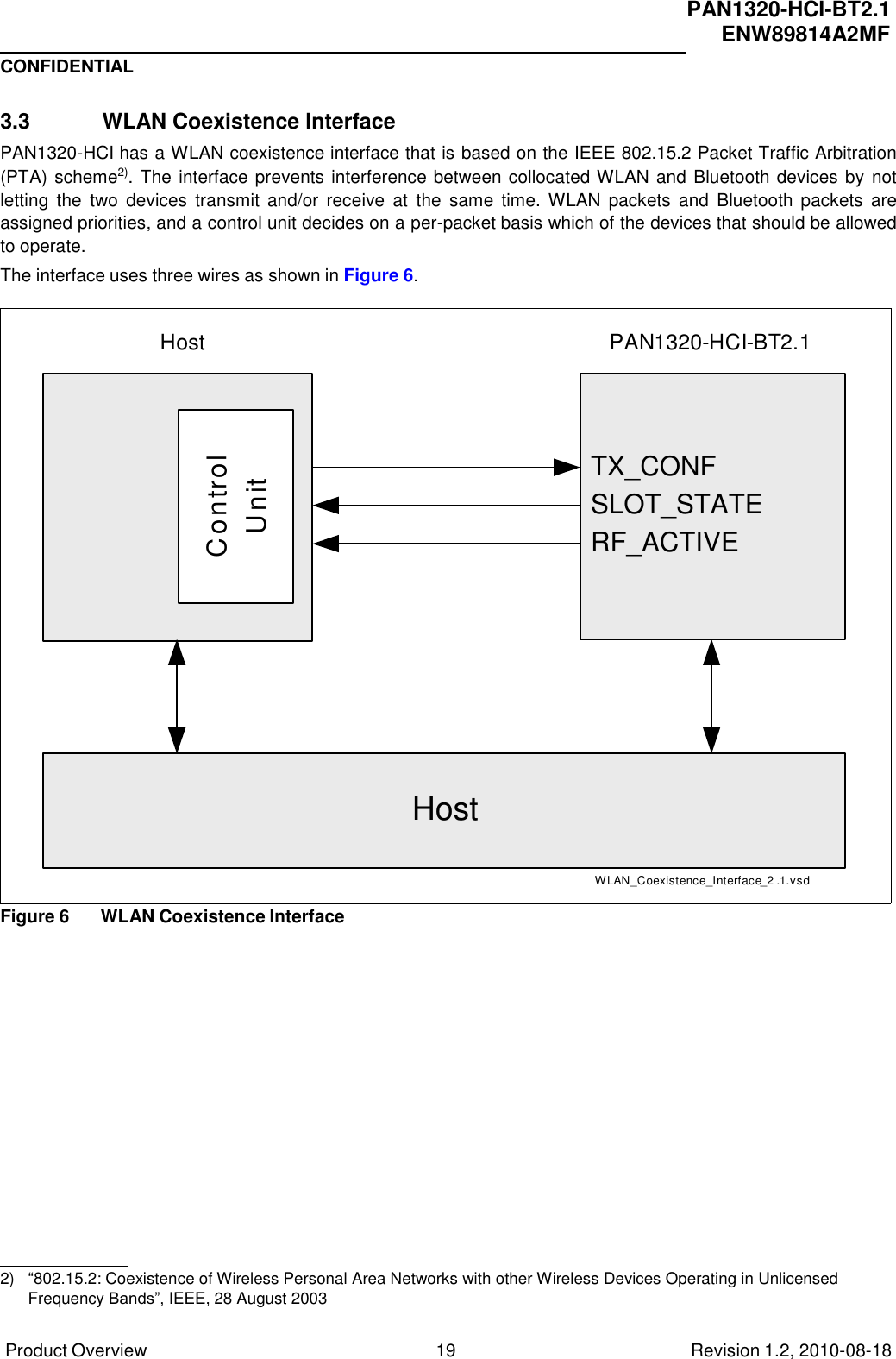
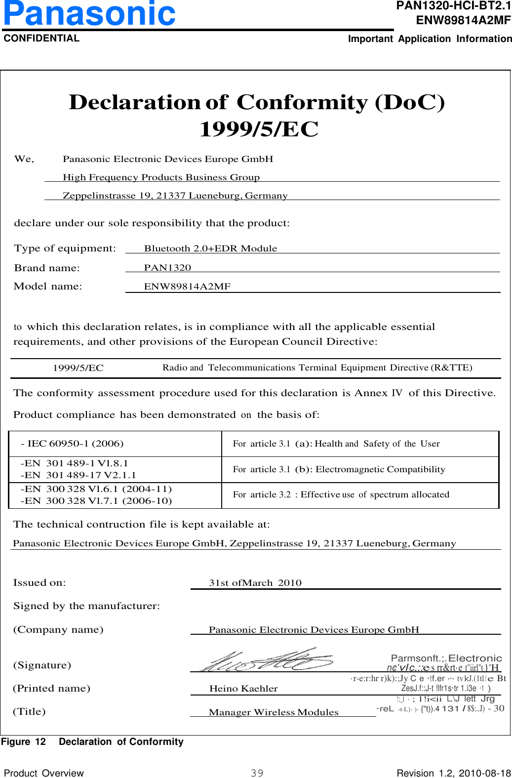
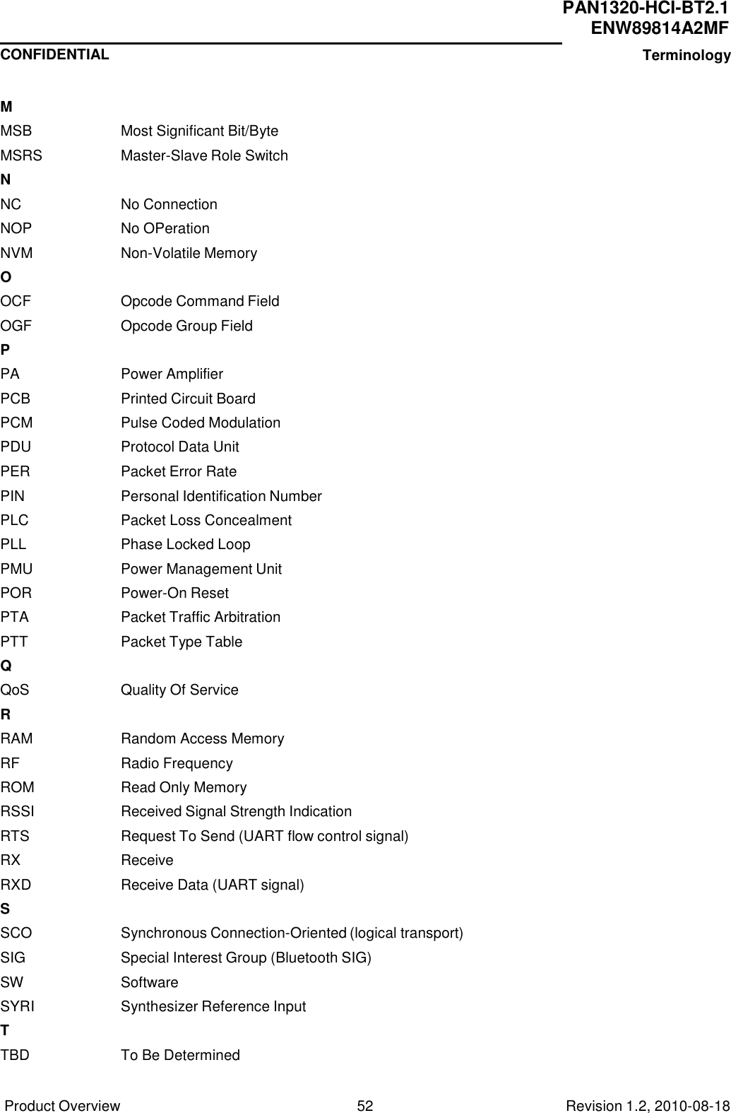
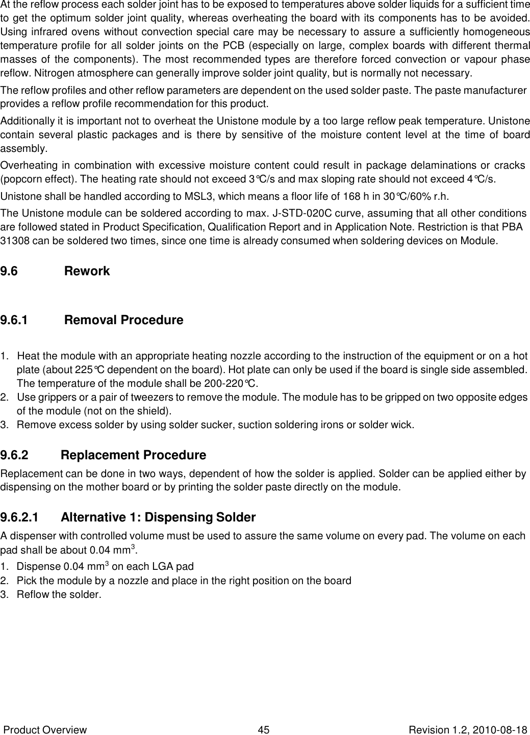
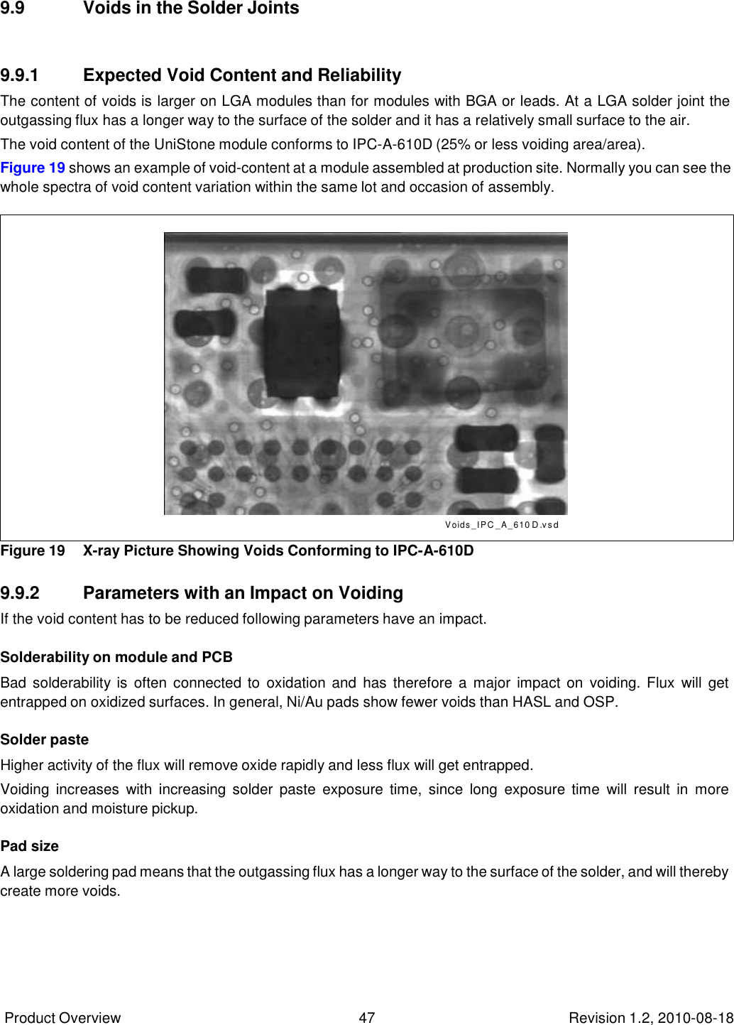
![Product Overview 44 Revision 1.2, 2010-08-18 9.5 Soldering Profile Generally all standard reflow soldering processes (vapour phase, convection, infrared) and typical temperature profiles used for surface mount devices are suitable for the Unistone module. Wave soldering is not possible. Figure 16 and Figure 17 shows example of a suitable solder reflow profile. One for leaded and one for leadfree solder. Recommended temp. profile for reflow soldering 10 ±1s 30 +20/-10s Temp.[°C] 235°C max. 220 ±5°C 200°C 150 ±10°C 90 ±30s Time [s] Figure 16 Eutectic Lead-Solder Profile Recommended temp. profile for reflow soldering (J-STD-020C) Temp.[°C] 260°C 255°C 217°C 30 sec max 200°C 60 ~ 150 sec 150°C 60 ~ 120 sec @ 3’C/sec max 6’C/sec max 25°C 8 minutes max Figure 17 Eutectic Leadfree-Solder Profile L ea dF ree _S old er _P rof ile .v s d Time [s]](https://usermanual.wiki/Panasonic-Devices-Europe/EBMU.15-PAN1320-UserMan-Rev1-2/User-Guide-2889704-Page-44.png)
![Product Overview 49 Revision 1.2, 2010-08-18 PAN1320-HCI-BT2.1 ENW89814A2MF CONFIDENTIAL References References [1] Panasonics User’s Manual - Firmware Description (BMU_PBA31308_V2.01_UM_FD_Rev1.2.pdf) This document is CONFIDENTIAL and can only distributed with NDA. [2] Panasonic User’s Manual - Hardware Description (PAN1320_V12.01_UM_HD_Rev1.4.pdf) This document is CONFIDENTIAL and can only distributed with NDA. [3] Infineon Generic Quality Specification for Mobile Phones (Generic Quality Specification for Mobile Phones V2.0_2007-08-16.pdf)](https://usermanual.wiki/Panasonic-Devices-Europe/EBMU.15-PAN1320-UserMan-Rev1-2/User-Guide-2889704-Page-49.png)