Panasonic Devices Europe EBMU Bluetooth Module User Manual PAN1320 BT2 1 PO
Panasonic Industrial Devices Europe GmbH Bluetooth Module PAN1320 BT2 1 PO
Contents
- 1. UserMan
- 2. 15_PAN1320 UserMan_Rev1.2
15_PAN1320 UserMan_Rev1.2

August
2010
ENW89814A2MF
Bluetooth QD ID:B014999 (BT V2.1 +EDR)
Bluetooth QD ID:B014940 (BT V2.0 +EDR)
Bluetooth
QD
ID:B014936
(BT
V1.2)
PAN1320-HCI-BT2.1
Infineon’s
BlueMoonUniversal
Platform
Wireless
Modules
Product Overview
R
e
v
i
s
i
o
n
1
.
2
, 2010-08-18
Edition 2010-08-18
Published by
Panasonic Industrial Devices Europe GmbH
Zeppelinstrasse 19
D-21337 Lüneburg, Germany
© 2010 Panasonic Industrial Devices Europe GmbH
All Rights Reserved.
Legal Disclaimer
The information given in this document shall in no event be regarded as a guarantee of conditions or
characteristics. With respect to any examples or hints given herein, any typical values stated herein and/or any
information regarding the application of the device, Infineon Technologies hereby disclaims any and all warranties
and liabilities of any kind, including without limitation, warranties of non-infringement of intellectual property rights
of any third party.
Information
For further information on technology, delivery terms and conditions and prices please contact your nearest
Panasonic Office in Germany or one of our Distributor or write an e-mail to wireless@eu.panasonic.com.
Warnings
Due to technical requirements components may contain dangerous substances. For information on the types in
question please contact your nearest Panasonic Office.
Panasonic Electronic Devices may only be used in life-support devices or systems with the express written
approval of Panasonic Devices, if a failure of such components can reasonably be expected to cause the failure
of that life-support device or system, or to affect the safety or effectiveness of that device or system. Life support
devices or systems are intended to be implanted in the human body, or to support and/or maintain and sustain
and/or protect human life. If they fail, it is reasonable to assume that the health of the user or other persons may
be endangered.

PAN1320-HCI-BT2.1
ENW89814A2MF
CONFIDENTIAL
Product Overview
3
Revision 1.2, 2010-08-18
ENW89814A2MF 12/01 BlueMoonTM Universal Platform
CONFIDENTIAL
Revision History: 2010-08-18, Revision 1.2
Previous Version: no former version where published
Page Subjects (major changes since last revision)
Rev1.2
Initial version
Trademarks of Infineon Technologies AG
ABM™, BlueMoon™, CONVERGATE™, COSIC™, C166™, FALC™, GEMINAX™, GOLDMOS™, ISAC™,
OMNITUNE™, OMNIVIA™, PROSOC™, SEROCCO™, SICOFI™, SIEGET™, SMARTi™, SMINT™,
SOCRATES™, VINAX™, VINETIC™, VOIPRO™, X-GOLD™, XMM™, X-PMU™, XWAY™
Other Trademarks
Microsoft®, Visio®, Windows®, Windows Vista®, Visual Studio®, Win32® of Microsoft Corporation. Linux® of
Linus Torvalds. FrameMaker®, Adobe® Reader™, Adobe Audition® of Adobe Systems Incorporated. APOXI®,
COMNEON™ of Comneon GmbH & Co. OHG. PrimeCell®, RealView®, ARM®, ARM® Developer Suite™ (ADS),
Multi-ICE™, ARM1176JZ-S™, CoreSight™, Embedded Trace Macrocell™ (ETM), Thumb®, ETM9™, AMBA™,
ARM7™, ARM9™, ARM7TDMI-S™, ARM926EJ-S™ of ARM Limited. OakDSPCore®, TeakLite® DSP Core,
OCEM® of ParthusCeva Inc. IndoorGPS™, GL-20000™, GL-LN-22™ of Global Locate. mipi™ of MIPI Alliance.
CAT-iq™ of DECT Forum. MIPS™, MIPS II™, 24KEc™, MIPS32®, 24KEc™ of MIPS Technologies, Inc. Texas
Instruments®, PowerPAD™, C62x™, C55x™, VLYNQ™, Telogy Software™, TMS320C62x™, Code Composer
Studio™, SSI™ of Texas Instruments Incorporated. Bluetooth® of Bluetooth SIG, Inc. IrDA® of the Infrared Data
Association. Java™, SunOS™, Solaris™ of Sun Microsystems, Inc. Philips®, I2C-Bus® of Koninklijke Philips
Electronics N.V. Epson® of Seiko Epson Corporation. Seiko® of Kabushiki Kaisha Hattori Seiko Corporation.
Panasonic® of Matsushita Electric Industrial Co., Ltd. Murata® of Murata Manufacturing Company. Taiyo Yuden™
of Taiyo Yuden Co., Ltd. TDK® of TDK Electronics Company, Ltd. Motorola® of Motorola, Inc. National
Semiconductor®, MICROWIRE™ of National Semiconductor Corporation. IEEE® of The Institute of Electrical and
Electronics Engineers, Inc. Samsung®, OneNAND®, UtRAM® of Samsung Corporation. Toshiba® of Toshiba
Corporation. Dallas Semiconductor®, 1-Wire® of Dallas Semiconductor Corp. ISO® of the International
Organization for Standardization. IEC™ of the International Engineering Consortium. EMV™ of EMVCo, LLC.
Zetex® of Zetex Semiconductors. Microtec® of Microtec Research, Inc. Verilog® of Cadence Design Systems, Inc.
ANSI® of the American National Standards Institute, Inc. WindRiver® and VxWorks® of Wind River Systems, Inc.
Nucleus™ of Mentor Graphics Corporation. OmniVision® of OmniVision Technologies, Inc. Sharp® of Sharp
Corporation. Symbian OS® of Symbian Software Ltd. Openwave® of Openwave Systems, Inc. Maxim® of Maxim
Integrated Products, Inc. Spansion® of Spansion LLC. Micron®, CellularRAM® of Micron Technology, Inc.
RFMD® of RF Micro Devices, Inc. EPCOS® of EPCOS AG. UNIX® of The Open Group. Tektronix® of Tektronix,
Inc. Intel® of Intel Corporation. Qimonda® of Qimonda AG. 1GOneNAND® of Samsung Corporation.
HyperTerminal® of Hilgraeve, Inc. MATLAB® of The MathWorks, Inc. Red Hat® of Red Hat, Inc. Palladium® of
Cadence Design Systems, Inc. SIRIUS Satellite Radio® of SIRIUS Satellite Radio Inc. TOKO® of TOKO Inc.
The information in this document is subject to change without notice.
Last Trademarks Update 2008-11-17

Product Overview
4
Revision 1.2, 2010-08-18
PAN1320-HCI-BT2.1
ENW89814A2MF
CONFIDENTIAL
Table of Contents
Table of Contents
Table of Contents . . . . . . . . . . . . . . . . . . . . . . . . . . . . . . . . . . . . . . . . . . . . . . . . . . . . . . . . . . . . . . . . 4
List of Figures . . . . . . . . . . . . . . . . . . . . . . . . . . . . . . . . . . . . . . . . . . . . . . . . . . . . . . . . . . . . . . . . . . . 6
List of Tables . . . . . . . . . . . . . . . . . . . . . . . . . . . . . . . . . . . . . . . . . . . . . . . . . . . . . . . . . . . . . . . . . . . . 7
1 General Device Overview . . . . . . . . . . . . . . . . . . . . . . . . . . . . . . . . . . . . . . . . . . . . . . . . . . . . . . . . . . 8
1.1 Features . . . . . . . . . . . . . . . . . . . . . . . . . . . . . . . . . . . . . . . . . . . . . . . . . . . . . . . . . . . . . . . . . . . . . . . . 8
1.2 Block Diagram . . . . . . . . . . . . . . . . . . . . . . . . . . . . . . . . . . . . . . . . . . . . . . . . . . . . . . . . . . . . . . . . . . . 9
1.3 Pin Configuration LGA . . . . . . . . . . . . . . . . . . . . . . . . . . . . . . . . . . . . . . . . . . . . . . . . . . . . . . . . . . . . . 9
1.4
Pin Description . . . . . . . . . . . . . . . . . . . . . . . . . . . . . . . . . . . . . . . . . . . . . . . . . . . . . . . . . . . . . . . . . .
10
1.5
System Integration . . . . . . . . . . . . . . . . . . . . . . . . . . . . . . . . . . . . . . . . . . . . . . . . . . . . . . . . . . . . . . .
12
1.6
FW version . . . . . . . . . . . . . . . . . . . . . . . . . . . . . . . . . . . . . . . . . . . . . . . . . . . . . . . . . . . . . . . . . . . . .
13
2
Basic Operating Information . . . . . . . . . . . . . . . . . . . . . . . . . . . . . . . . . . . . . . . . . . . . . . . . . . . . . .
14
2.1
Power Supply . . . . . . . . . . . . . . . . . . . . . . . . . . . . . . . . . . . . . . . . . . . . . . . . . . . . . . . . . . . . . . . . . . .
14
2.2
Clocking . . . . . . . . . . . . . . . . . . . . . . . . . . . . . . . . . . . . . . . . . . . . . . . . . . . . . . . . . . . . . . . . . . . . . . .
14
3
Interfaces . . . . . . . . . . . . . . . . . . . . . . . . . . . . . . . . . . . . . . . . . . . . . . . . . . . . . . . . . . . . . . . . . . . . . .
15
3.1
HCI / UART Interface . . . . . . . . . . . . . . . . . . . . . . . . . . . . . . . . . . . . . . . . . . . . . . . . . . . . . . . . . . . . .
15
3.1.1
Supported Transport Layers . . . . . . . . . . . . . . . . . . . . . . . . . . . . . . . . . . . . . . . . . . . . . . . . . . . . . .
15
3.1.2
UART . . . . . . . . . . . . . . . . . . . . . . . . . . . . . . . . . . . . . . . . . . . . . . . . . . . . . . . . . . . . . . . . . . . . . . . .
15
3.1.2.1
Baud Rates . . . . . . . . . . . . . . . . . . . . . . . . . . . . . . . . . . . . . . . . . . . . . . . . . . . . . . . . . . . . . . . . .
15
3.2
PCM Interface . . . . . . . . . . . . . . . . . . . . . . . . . . . . . . . . . . . . . . . . . . . . . . . . . . . . . . . . . . . . . . . . . . .
17
3.2.1
Overview . . . . . . . . . . . . . . . . . . . . . . . . . . . . . . . . . . . . . . . . . . . . . . . . . . . . . . . . . . . . . . . . . . . . .
17
3.3
WLAN Coexistence Interface . . . . . . . . . . . . . . . . . . . . . . . . . . . . . . . . . . . . . . . . . . . . . . . . . . . . . . .
19
4
General Device Capabilities . . . . . . . . . . . . . . . . . . . . . . . . . . . . . . . . . . . . . . . . . . . . . . . . . . . . . . .
20
4.1
HCI+ and Bluetooth Device Data (BD_DATA) . . . . . . . . . . . . . . . . . . . . . . . . . . . . . . . . . . . . . . . . . .
20
4.2
Manufacturer Mode . . . . . . . . . . . . . . . . . . . . . . . . . . . . . . . . . . . . . . . . . . . . . . . . . . . . . . . . . . . . . . .
20
4.3
Firmware ROM Patching . . . . . . . . . . . . . . . . . . . . . . . . . . . . . . . . . . . . . . . . . . . . . . . . . . . . . . . . . .
20
4.3.1
Patch Support . . . . . . . . . . . . . . . . . . . . . . . . . . . . . . . . . . . . . . . . . . . . . . . . . . . . . . . . . . . . . . . . .
20
5
Bluetooth Capabilities . . . . . . . . . . . . . . . . . . . . . . . . . . . . . . . . . . . . . . . . . . . . . . . . . . . . . . . . . . .
21
5.1
Supported Features . . . . . . . . . . . . . . . . . . . . . . . . . . . . . . . . . . . . . . . . . . . . . . . . . . . . . . . . . . . . . .
21
5.2
Not-supported Features . . . . . . . . . . . . . . . . . . . . . . . . . . . . . . . . . . . . . . . . . . . . . . . . . . . . . . . . . . .
21
5.3
PAN1320-HCI Specifics and Extensions . . . . . . . . . . . . . . . . . . . . . . . . . . . . . . . . . . . . . . . . . . . . . .
21
5.3.1
During Connection . . . . . . . . . . . . . . . . . . . . . . . . . . . . . . . . . . . . . . . . . . . . . . . . . . . . . . . . . . . . . .
21
5.3.1.1
Scatternet and Piconet Capabilities . . . . . . . . . . . . . . . . . . . . . . . . . . . . . . . . . . . . . . . . . . . . . . .
21
5.3.1.2
Role Switch . . . . . . . . . . . . . . . . . . . . . . . . . . . . . . . . . . . . . . . . . . . . . . . . . . . . . . . . . . . . . . . . .
22
5.3.1.3
Dynamic Polling Strategy . . . . . . . . . . . . . . . . . . . . . . . . . . . . . . . . . . . . . . . . . . . . . . . . . . . . . . .
22
5.3.1.4
Adaptive Frequency Hopping (AFH) . . . . . . . . . . . . . . . . . . . . . . . . . . . . . . . . . . . . . . . . . . . . . .
22
5.3.1.5
Channel Quality Driven Data Rate Change (CQDDR) . . . . . . . . . . . . . . . . . . . . . . . . . . . . . . . .
22
5.3.2
Synchronous Links . . . . . . . . . . . . . . . . . . . . . . . . . . . . . . . . . . . . . . . . . . . . . . . . . . . . . . . . . . . . .
22
5.3.2.1
Interface . . . . . . . . . . . . . . . . . . . . . . . . . . . . . . . . . . . . . . . . . . . . . . . . . . . . . . . . . . . . . . . . . . . .
22
5.3.2.2
Voice Coding . . . . . . . . . . . . . . . . . . . . . . . . . . . . . . . . . . . . . . . . . . . . . . . . . . . . . . . . . . . . . . . .
24
5.3.3
RSSI and Output Power Control . . . . . . . . . . . . . . . . . . . . . . . . . . . . . . . . . . . . . . . . . . . . . . . . . . .
24
5.3.3.1
Received Signal Strength Indication (RSSI) . . . . . . . . . . . . . . . . . . . . . . . . . . . . . . . . . . . . . . . .
24
5.3.3.2
Output Power Control . . . . . . . . . . . . . . . . . . . . . . . . . . . . . . . . . . . . . . . . . . . . . . . . . . . . . . . . .
24
5.3.3.3
Ultra Low Transmit Power . . . . . . . . . . . . . . . . . . . . . . . . . . . . . . . . . . . . . . . . . . . . . . . . . . . . . .
24
6
Electrical Characteristics . . . . . . . . . . . . . . . . . . . . . . . . . . . . . . . . . . . . . . . . . . . . . . . . . . . . . . . . .
25
6.1
Absolute Maximum Ratings . . . . . . . . . . . . . . . . . . . . . . . . . . . . . . . . . . . . . . . . . . . . . . . . . . . . . . . .
25
6.2
Operating Conditions . . . . . . . . . . . . . . . . . . . . . . . . . . . . . . . . . . . . . . . . . . . . . . . . . . . . . . . . . . . . .
25

Product Overview
5
Revision 1.2, 2010-08-18
PAN1320-HCI-BT2.1
ENW89814A2MF
CONFIDENTIAL
Table of Contents
6.3
DC Characteristics . . . . . . . . . . . . . . . . . . . . . . . . . . . . . . . . . . . . . . . . . . . . . . . . . . . . . . . . . . . . . . .
26
6.3.1
Pad Driver and Input Stages . . . . . . . . . . . . . . . . . . . . . . . . . . . . . . . . . . . . . . . . . . . . . . . . . . . . . .
26
6.3.2
Pull-ups and Pull-downs . . . . . . . . . . . . . . . . . . . . . . . . . . . . . . . . . . . . . . . . . . . . . . . . . . . . . . . . .
28
6.3.3
Protection Circuits . . . . . . . . . . . . . . . . . . . . . . . . . . . . . . . . . . . . . . . . . . . . . . . . . . . . . . . . . . . . . .
28
6.3.4
System Power Consumption . . . . . . . . . . . . . . . . . . . . . . . . . . . . . . . . . . . . . . . . . . . . . . . . . . . . . .
29
6.4
AC Characteristics . . . . . . . . . . . . . . . . . . . . . . . . . . . . . . . . . . . . . . . . . . . . . . . . . . . . . . . . . . . . . . .
29
6.4.1
Characteristics of 32.768 kHz Clock Signal . . . . . . . . . . . . . . . . . . . . . . . . . . . . . . . . . . . . . . . . . . .
30
6.5
RF Part . . . . . . . . . . . . . . . . . . . . . . . . . . . . . . . . . . . . . . . . . . . . . . . . . . . . . . . . . . . . . . . . . . . . . . . .
30
6.5.1
Characteristics RF Part . . . . . . . . . . . . . . . . . . . . . . . . . . . . . . . . . . . . . . . . . . . . . . . . . . . . . . . . . .
30
6.5.1.1
Bluetooth Related Specifications . . . . . . . . . . . . . . . . . . . . . . . . . . . . . . . . . . . . . . . . . . . . . . . . .
30
7
Package Information . . . . . . . . . . . . . . . . . . . . . . . . . . . . . . . . . . . . . . . . . . . . . . . . . . . . . . . . . . . .
34
7.1
Package Marking . . . . . . . . . . . . . . . . . . . . . . . . . . . . . . . . . . . . . . . . . . . . . . . . . . . . . . . . . . . . . . . .
34
7.2
Production Package . . . . . . . . . . . . . . . . . . . . . . . . . . . . . . . . . . . . . . . . . . . . . . . . . . . . . . . . . . . . . .
34
7.2.1
Pin Mark . . . . . . . . . . . . . . . . . . . . . . . . . . . . . . . . . . . . . . . . . . . . . . . . . . . . . . . . . . . . . . . . . . . . . .
35
8
Important Application Information . . . . . . . . . . . . . . . . . . . . . . . . . . . . . . . . . . . . . . . . . . . . . . . . .
36
8.1
Reference Design . . . . . . . . . . . . . . . . . . . . . . . . . . . . . . . . . . . . . . . . . . . . . . . . . . . . . . . . . . . . . . . .
36
8.2
FCC Class B Digital Devices Regulatory Notice . . . . . . . . . . . . . . . . . . . . . . . . . . . . . . . . . . . . . . . . .
37
8.3
FCC Wireless Notice . . . . . . . . . . . . . . . . . . . . . . . . . . . . . . . . . . . . . . . . . . . . . . . . . . . . . . . . . . . . .
37
8.4
FCC Interference Statement . . . . . . . . . . . . . . . . . . . . . . . . . . . . . . . . . . . . . . . . . . . . . . . . . . . . . . . .
38
8.5
FCC Identifier . . . . . . . . . . . . . . . . . . . . . . . . . . . . . . . . . . . . . . . . . . . . . . . . . . . . . . . . . . . . . . . . . . .
38
8.6
European R&TTE Declaration of Conformity . . . . . . . . . . . . . . . . . . . . . . . . . . . . . . . . . . . . . . . . . . .
38
8.7
Bluetooth Qualified Design ID . . . . . . . . . . . . . . . . . . . . . . . . . . . . . . . . . . . . . . . . . . . . . . . . . . . . . . .
40
8.8
Industry Canada Certification . . . . . . . . . . . . . . . . . . . . . . . . . . . . . . . . . . . . . . . . . . . . . . . . . . . . . . .
40
8.9
Label Design of the Host Product . . . . . . . . . . . . . . . . . . . . . . . . . . . . . . . . . . . . . . . . . . . . . . . . . . . .
40
8.10
Regulatory Test House . . . . . . . . . . . . . . . . . . . . . . . . . . . . . . . . . . . . . . . . . . . . . . . . . . . . . . . . . . . .
40
9
Assembly Guidelines . . . . . . . . . . . . . . . . . . . . . . . . . . . . . . . . . . . . . . . . . . . . . . . . . . . . . . . . . . . .
41
9.1
General Description of the Module . . . . . . . . . . . . . . . . . . . . . . . . . . . . . . . . . . . . . . . . . . . . . . . . . . .
41
9.2
Printed Circuit Board Design . . . . . . . . . . . . . . . . . . . . . . . . . . . . . . . . . . . . . . . . . . . . . . . . . . . . . . .
41
9.3
Solder Paste Printing . . . . . . . . . . . . . . . . . . . . . . . . . . . . . . . . . . . . . . . . . . . . . . . . . . . . . . . . . . . . .
42
9.4
Assembly . . . . . . . . . . . . . . . . . . . . . . . . . . . . . . . . . . . . . . . . . . . . . . . . . . . . . . . . . . . . . . . . . . . . . .
42
9.4.1
Component Placement . . . . . . . . . . . . . . . . . . . . . . . . . . . . . . . . . . . . . . . . . . . . . . . . . . . . . . . . . .
42
9.4.2
Pin Mark . . . . . . . . . . . . . . . . . . . . . . . . . . . . . . . . . . . . . . . . . . . . . . . . . . . . . . . . . . . . . . . . . . . . . .
42
9.4.3
Package . . . . . . . . . . . . . . . . . . . . . . . . . . . . . . . . . . . . . . . . . . . . . . . . . . . . . . . . . . . . . . . . . . . . . .
43
9.5
Soldering Profile . . . . . . . . . . . . . . . . . . . . . . . . . . . . . . . . . . . . . . . . . . . . . . . . . . . . . . . . . . . . . . . . .
44
9.6
Rework . . . . . . . . . . . . . . . . . . . . . . . . . . . . . . . . . . . . . . . . . . . . . . . . . . . . . . . . . . . . . . . . . . . . . . . .
45
9.6.1
Removal Procedure . . . . . . . . . . . . . . . . . . . . . . . . . . . . . . . . . . . . . . . . . . . . . . . . . . . . . . . . . . . .
45
9.6.2
Replacement Procedure . . . . . . . . . . . . . . . . . . . . . . . . . . . . . . . . . . . . . . . . . . . . . . . . . . . . . . . . .
45
9.6.2.1
Alternative 1: Dispensing Solder . . . . . . . . . . . . . . . . . . . . . . . . . . . . . . . . . . . . . . . . . . . . . . . . .
45
9.6.2.2
Alternative 2: Printing Solder . . . . . . . . . . . . . . . . . . . . . . . . . . . . . . . . . . . . . . . . . . . . . . . . . . . .
46
9.7
Inspection . . . . . . . . . . . . . . . . . . . . . . . . . . . . . . . . . . . . . . . . . . . . . . . . . . . . . . . . . . . . . . . . . . . . . .
46
9.8
Component Salvage . . . . . . . . . . . . . . . . . . . . . . . . . . . . . . . . . . . . . . . . . . . . . . . . . . . . . . . . . . . . . .
46
9.9
Voids in the Solder Joints . . . . . . . . . . . . . . . . . . . . . . . . . . . . . . . . . . . . . . . . . . . . . . . . . . . . . . . . . .
47
9.9.1
Expected Void Content and Reliability . . . . . . . . . . . . . . . . . . . . . . . . . . . . . . . . . . . . . . . . . . . . . . .
47
9.9.2
Parameters with an Impact on Voiding . . . . . . . . . . . . . . . . . . . . . . . . . . . . . . . . . . . . . . . . . . . . . .
47
References . . . . . . . . . . . . . . . . . . . . . . . . . . . . . . . . . . . . . . . . . . . . . . . . . . . . . . . . . . . . . . . . . . . .
49
Terminology . . . . . . . . . . . . . . . . . . . . . . . . . . . . . . . . . . . . . . . . . . . . . . . . . . . . . . . . . . . . . . . . . . .
50

Product Overview
6
Revision 1.2, 2010-08-18
PAN1320-HCI-BT2.1
ENW89814A2MF
CONFIDENTIAL List of Figures
List of Figures
Figure 1 Simplified Block Diagram of PAN1320-HCI . . . . . . . . . . . . . . . . . . . . . . . . . . . . . . . . . . . . . . . . . . . 9
Figure 2 Pin Configuration for PAN1320-HCI in Top View
(footprint)
. . . . . . . . . . . . . . . . . . . . . . . . . . . . . . . 9
Figure 3 Example of a Bluetooth System . . . . . . . . . . . . . . . . . . . . . . . . . . . . . . . . . . . . . . . . . . . . . . . . . . . 12
Figure 4 HCI/UART Interface . . . . . . . . . . . . . . . . . . . . . . . . . . . . . . . . . . . . . . . . . . . . . . . . . . . . . . . . . . . . 15
Figure 5
PCM_Signals_Overview
. . . . . . . . . . . . . . . . . . . . . . . . . . . . . . . . . . . . . . . . . . . . . . . . . . . . . . . . . 17
Figure 6 WLAN Coexistence Interface . . . . . . . . . . . . . . . . . . . . . . . . . . . . . . . . . . . . . . . . . . . . . . . . . . . . . 19
Figure 7 Package Marking . . . . . . . . . . . . . . . . . . . . . . . . . . . . . . . . . . . . . . . . . . . . . . . . . . . . . . . . . . . . . . 34
Figure 8 Production Package . . . . . . . . . . . . . . . . . . . . . . . . . . . . . . . . . . . . . . . . . . . . . . . . . . . . . . . . . . . . 34
Figure 9 Top View and Bottom View. . . . . . . . . . . . . . . . . . . . . . . . . . . . . . . . . . . . . . . . . . . . . . . . . . . . . . . 35
Figure 10 Reference Design Schematics . . . . . . . . . . . . . . . . . . . . . . . . . . . . . . . . . . . . . . . . . . . . . . . . . . . . 36
Figure 11 Equipment Label. . . . . . . . . . . . . . . . . . . . . . . . . . . . . . . . . . . . . . . . . . . . . . . . . . . . . . . . . . . . . . . 38
Figure 12 Declaration of
Conformity
. . . . . . . . . . . . . . . . . . . . . . . . . . . . . . . . . . . . . . . . . . . . . . . . . . . . . . . . 39
Figure 13 Pad Layout on the Module (Top View) . . . . . . . . . . . . . . . . . . . . . . . . . . . . . . . . . . . . . . . . . . . . . . 41
Figure 14 Pin Marking. . . . . . . . . . . . . . . . . . . . . . . . . . . . . . . . . . . . . . . . . . . . . . . . . . . . . . . . . . . . . . . . . . . 42
Figure 15 Tape on Reel . . . . . . . . . . . . . . . . . . . . . . . . . . . . . . . . . . . . . . . . . . . . . . . . . . . . . . . . . . . . . . . . . 43
Figure 16 Eutectic Lead-Solder
Profile
. . . . . . . . . . . . . . . . . . . . . . . . . . . . . . . . . . . . . . . . . . . . . . . . . . . . . . 44
Figure 17 Eutectic Leadfree-Solder
Profile
. . . . . . . . . . . . . . . . . . . . . . . . . . . . . . . . . . . . . . . . . . . . . . . . . . . 44
Figure 18 Solder Printing . . . . . . . . . . . . . . . . . . . . . . . . . . . . . . . . . . . . . . . . . . . . . . . . . . . . . . . . . . . . . . . . 46
Figure 19 X-ray Picture Showing Voids Conforming to IPC-A-610D . . . . . . . . . . . . . . . . . . . . . . . . . . . . . . . 47

Product Overview
7
Revision 1.2, 2010-08-18
PAN1320-HCI-BT2.1
ENW89814A2MF
CONFIDENTIAL List of Tables
List of Tables
Table 1 Pin Description . . . . . . . . . . . . . . . . . . . . . . . . . . . . . . . . . . . . . . . . . . . . . . . . . . . . . . . . . . . . . . . . 10
Table 2 UART Baud Rates . . . . . . . . . . . . . . . . . . . . . . . . . . . . . . . . . . . . . . . . . . . . . . . . . . . . . . . . . . . . . 15
Table 3 Supported Voice Settings . . . . . . . . . . . . . . . . . . . . . . . . . . . . . . . . . . . . . . . . . . . . . . . . . . . . . . . 24
Table 4 Absolute Maximum Ratings . . . . . . . . . . . . . . . . . . . . . . . . . . . . . . . . . . . . . . . . . . . . . . . . . . . . . . 25
Table 5 Operating Conditions . . . . . . . . . . . . . . . . . . . . . . . . . . . . . . . . . . . . . . . . . . . . . . . . . . . . . . . . . . . 25
Table 6 Internal1 (1.5 V) Supplied Pins . . . . . . . . . . . . . . . . . . . . . . . . . . . . . . . . . . . . . . . . . . . . . . . . . . . 26
Table 7 Internal2 (2.5 V) Supplied Pins . . . . . . . . . . . . . . . . . . . . . . . . . . . . . . . . . . . . . . . . . . . . . . . . . . . 26
Table 8 VDDUART Supplied Pins . . . . . . . . . . . . . . . . . . . . . . . . . . . . . . . . . . . . . . . . . . . . . . . . . . . . . . . 26
Table 9 VDDPCM Supplied Pins . . . . . . . . . . . . . . . . . . . . . . . . . . . . . . . . . . . . . . . . . . . . . . . . . . . . . . . . 27
Table 10 ONOFF PIN . . . . . . . . . . . . . . . . . . . . . . . . . . . . . . . . . . . . . . . . . . . . . . . . . . . . . . . . . . . . . . . . . . 27
Table 11 Pull-up and Pull-down Currents . . . . . . . . . . . . . . . . . . . . . . . . . . . . . . . . . . . . . . . . . . . . . . . . . . . 28
Table 12 Current Consumption in Different Operating Modes . . . . . . . . . . . . . . . . . . . . . . . . . . . . . . . . . . . 29
Table 13 Max. Load at the Different Supply Voltages . . . . . . . . . . . . . . . . . . . . . . . . . . . . . . . . . . . . . . . . . 29
Table 14 PCM Interface Timing . . . . . . . . . . . . . . . . . . . . . . . . . . . . . . . . . . . . . . . . . . . . . . . . . . . . . . . . . . 29
Table 15 Timing Characteristics of PCM Interface for the First Bit . . . . . . . . . . . . . . . . . . . . . . . . . . . . . . . . 30
Table 16 BDR - Transmitter Part . . . . . . . . . . . . . . . . . . . . . . . . . . . . . . . . . . . . . . . . . . . . . . . . . . . . . . . . . 30
Table 17 BDR -Receiver Part . . . . . . . . . . . . . . . . . . . . . . . . . . . . . . . . . . . . . . . . . . . . . . . . . . . . . . . . . . . . 31
Table 18 EDR - Transmitter Part . . . . . . . . . . . . . . . . . . . . . . . . . . . . . . . . . . . . . . . . . . . . . . . . . . . . . . . . . 32
Table 19 EDR -Receiver Part . . . . . . . . . . . . . . . . . . . . . . . . . . . . . . . . . . . . . . . . . . . . . . . . . . . . . . . . . . . . 33
Table 20 Antennas. . . . . . . . . . . . . . . . . . . . . . . . . . . . . . . . . . . . . . . . . . . . . . . . . . . . . . . . . . . . . . . . . . . . . 37

Product Overview
8
Revision 1.2, 2010-08-18
PAN1320-HCI-BT2.1
ENW89814A2MF
CONFIDENTIAL
General Device Overview
1
General Device Overview
1.1 Features
General
• Complete Bluetooth 2.1 + EDR solution
– Configurable for BT 1.2 and 2.0 +
EDR
• Ultra low power design in 0.13 μm CMOS
• Temperature range from -40°C to 85°C
• Integrates ARM7TDMI, RAM and patchable ROM
• On-module voltage regulators. External supply 2.9 - 4.1 V
• On-module EEPROM with configuration data
• Reference clock included
• Low power clock from internal oscillator or external low power clock (e.g. 32.768 kHz)
• Dynamic low power mode switching
Interfaces
• 3.25 MBaud UART with transport layer detection (HCI UART, HCI Three-Wire UART)
• PCM/I2S interface for digital audio
• WLAN coexistence interface
• General purpose I/Os with interrupt capabilities. JTAG for boundary scan and debug
RF
• Transmit power programmable from -45 dBm to 4.5 dBm
• Transmit power typ. 2.5 dBm (default settings)
• Receiver sensitivity typ. -86 dBm
• Integrated antenna switch, balun and antenna filter
• Integrated LNA with excellent blocking and intermodulation performance
• No external components except antenna
• Digital demodulation for optimum sensitivity and co-/adjacent channel performance
Bluetooth
• Piconet with seven slaves. Scatternet with two slave roles while still being discoverable
• SCO and eSCO with hardware accelerated audio signal processing
• Audio error correction algorithm (PLC) improving speech quality
• Power control and RSSI. Hold and Sniff.
• Adaptive Frequency Hopping, Quality of Service, Channel Quality Driven Data Rate
• Bluetooth security features: Authentication, Pairing, Encryption and Secure Simple Pairing
• Bluetooth test mode
• Sniff Subrating for lower Sniff power consumption
Product Overview
9
Revision 1.2, 2010-08-18
PAN1320-HCI-BT2.1
ENW89814A2MF
CONFIDENTIAL
General Device Overview
1.2
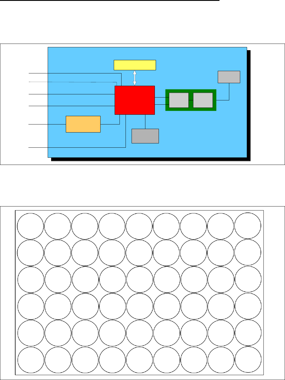
Block Diagram
PAN1320
-HCI-BT2.1
EEPROM
VDD_PCM
VDD_UART
I2C
Ceramic
Antenna
UART - HCI
PCM1
PMB8763
BlueMoon
UniCellular
Balun Filter
Vsupply
Low Power Clock
(Optional)
32.768 kHz
Voltage
Regulator
Crystal
26 MHz
Figure 1 Simplified Block Diagram of PAN1320-HCI
1.3 Pin Configuration LGA
F2
F1 P1 .2 F3
P0.1 1 F4
P0. 1 4 F5
P0.7 F6 F7
P0 .4
F8
P0. 6 F9
VSS TDI
RF_ ACTIVE TX _CONF TX _CONF UARTCTS VDDUART UARTTXD UARTRTS VSS
E1
P0. 1 2
SDAO
E2
P0. 1 3
SCL O
E3
P1.3
TDO
SL OT_STATE
E4
P0 .0
PCMFR1
E5
P0 .1
PCMCL K
E6
P0 .5 E7
UARTRXD NC
E8
VSS
E9
VSS
D1
P0 .1 0
D2
P0 .8
D3
P1. 1
TCK
D4
P0 .3
PCMOUT
D5
P0.2 D6
PCMIN NC
D7
VSS
D8 D9
VSS NC
C1
C2
C3
C4
C5
C6
C7
C8
C9
VREG
P0 .9
JTAG #
TRST#
VDDPCM
NC
NC
VSS
VSS
B1
P1.7
WAKEUP _ BT
A1
VSS
B2
P1 .8
WAKEUP _
HOST
A2
P1.8
B3
P1 .0
TMS
A3
RESET #
B4
P1.4
RTCK
A4
VSUPPL Y
B5
ONOFF
A5
VSUPPLY
B6
NC
A6
VSUPPL Y
B7
NC
A7
VSS
B8
NC
A8
P1. 5
CL K3 2
B9
SL EEPX
A9
VSS
Figure 2 Pin Configuration for PAN1320-HCI in Top View (footprint)

PAN1320-HCI-BT2.1
ENW89814A2MF
CONFIDENTIAL
General Device Overview
Product Overview
10
Revision 1.2, 2010-08-18
1.4 Pin Description
The
non-shaded
cells indicate pins that will be fixed for the product lifetime. Shaded cells indicate that the pin might
be removed/changed in future variants. All pins not listed below shall be not connected.
Table 1 Pin Description
Pin
No.
Symbol
Input /
Output
Supply Voltage
During
Reset
After
Reset
Function
A2
P1.6
I/O/OD
Internal1
Z
Z
Port 1.6
A3
RESET#
AI
Internal1
Input
Input
Hardware Reset
A8
P1.5/
CLK32
I/O/OD
Internal1
Input
Input
Port 1.5 or
LPM clock input (e.g.
32.768 kHz)
B1
P1.7/
WAKEUP_BT
I/O/OD
Internal1
PD/
Input
PD/ Input
Port 1.7 or
Bluetooth wake-up signal
B2
P1.8/
WAKEUP_HOST
I/O/OD
Internal1
PD
PD
Port 1.8 or
Host wake-up signal
B3
P1.0/
TMS
I/O/OD
Internal2
PU
1)
PU
1)
Port 1.0 or
JTAG interface
B4
P1.4/
RTCK
I/O/OD
Internal2
Z
Z
Port 1.4 or
JTAG interface
B5
ONOFF
I
-
-
Turns off module completely
B9
SLEEPX
I/O
VDDUART
PD
H
Sleep indication signal
C2
P0.9
I/O/OD
Internal2
Z
Z
Port 0.9
C3
JTAG#
I
Internal2
PU
PU
Mode selection Port 1:
0: JTAG
1: Port
C4
TRST#
I
Internal2
PD
PD
JTAG interface
D1
P0.10
I/O/OD
Internal2
Z
Z
Port 0.10
D2
P0.8
I/O/OD
Internal2
PD
PD
Port 0.8
D3
P1.1/
TCK
I/O/OD
Internal2
PU
1)
PU
1)
Port 1.1 or
JTAG interface
D4
P0.3/
PCMOUT
I/O/OD
VDDPCM
Conf.
PD def.
Conf.
PD def.
Port 0.3 or
PCM data out
D5
P0.2/
PCMIN
I/O/OD
VDDPCM
Z
Z
Port 0.2 or
PCM data in
E1
P0.12/
SDA0
I/O/OD
Internal2
PU
PU
Port 0.12 or
I2C data signal
E2
P0.13/
SCL0
I/O/OD
Internal2
PU
PU
Port 0.13 or
I2C clock signal
E3
P1.3/ TDO/
SLOT_STATE
I/O/OD
Internal2
Z
Z
Port 1.3 or
JTAG interface or
WLAN coexistence interface
E4
P0.0/
PCMFR1
I/O/OD
VDDPCM
PD
PD
Port 0.0 or
PCM frame signal 1

PAN1320-HCI-BT2.1
ENW89814A2MF
CONFIDENTIAL
General Device Overview
Product Overview
11
Revision 1.2, 2010-08-18
Table 1 Pin Description
Pin
No.
Symbol
Input /
Output
Supply Voltage
During
Reset
After
Reset
Function
E5
P0.1/
PCMCLK
I/O/OD
VDDPCM
PD
PD
Port 0.1 or
PCM clock
E6
P0.5/
UARTRXD
I/O/OD
VDDUART
Z
Z
Port 0.5 or
UART receive data
F2
P1.2/ TDI/
RF_ACTIVE
I/O/OD
Internal2
PU
1)
PU
1)
Port 1.2 or
JTAG interface or
WLAN coexistence interface
F3
P0.11/
TX_CONF
I/O/OD
Internal2
Z
Z
Port 0.11or
WLAN coexistence interface
F4
P0.14/
TX_CONF
I/O
VDDUART
Z
Z
Port 0.14 or
WLAN coexistence interface
F5
P0.7/
UARTCTS
I/O/OD
VDDUART
Z
Z
Port 0.7 or
UART CTS flow control
F7
P0.4/
UARTTXD
I/O/OD
VDDUART
PU
PU
Port 0.4 or
UART transmit data
F8
P0.6/
UARTRTS
I/O/OD
VDDUART
PU
PU
Port 0.6 or
UART RTS flow control
A4,
A5,
A6
VSUPPLY
SI
-
-
Power supply
C1
VREG
SO
-
-
Regulated Power supply
F6
VDDUART
SI
-
-
UART interface Power supply
C5
VDDPCM
SI
-
-
PCM interface Power supply
A1,
A7,
A9,
C8,
C9,
D7,
D8,
E8,
E9,
F1,
F9
VSS
-
-
Ground
1) Fixed pull-up/pull-down if JTAG interface is selected, not affected by any chip reset. If JTAG interface is not selected the
port is tristate.
PAN1320-HCI-BT2.1
ENW89814A2MF
CONFIDENTIAL
General Device Overview
Product Overview
12
Revision 1.2, 2010-08-18
PCM/ I2S
UART
VDDSUP
VDDUART
VDDPCM
Descriptions of acronyms used in the pin list:
Acronym
Description
I
Input
O
Output
OD
Output with open drain capability
Z
Tristate
PU
Pull-up
PD
Pull-down
A
Analog (e.g. AI means analog input)
S
Supply (e.g. SO means supply output)
1.5 System Integration
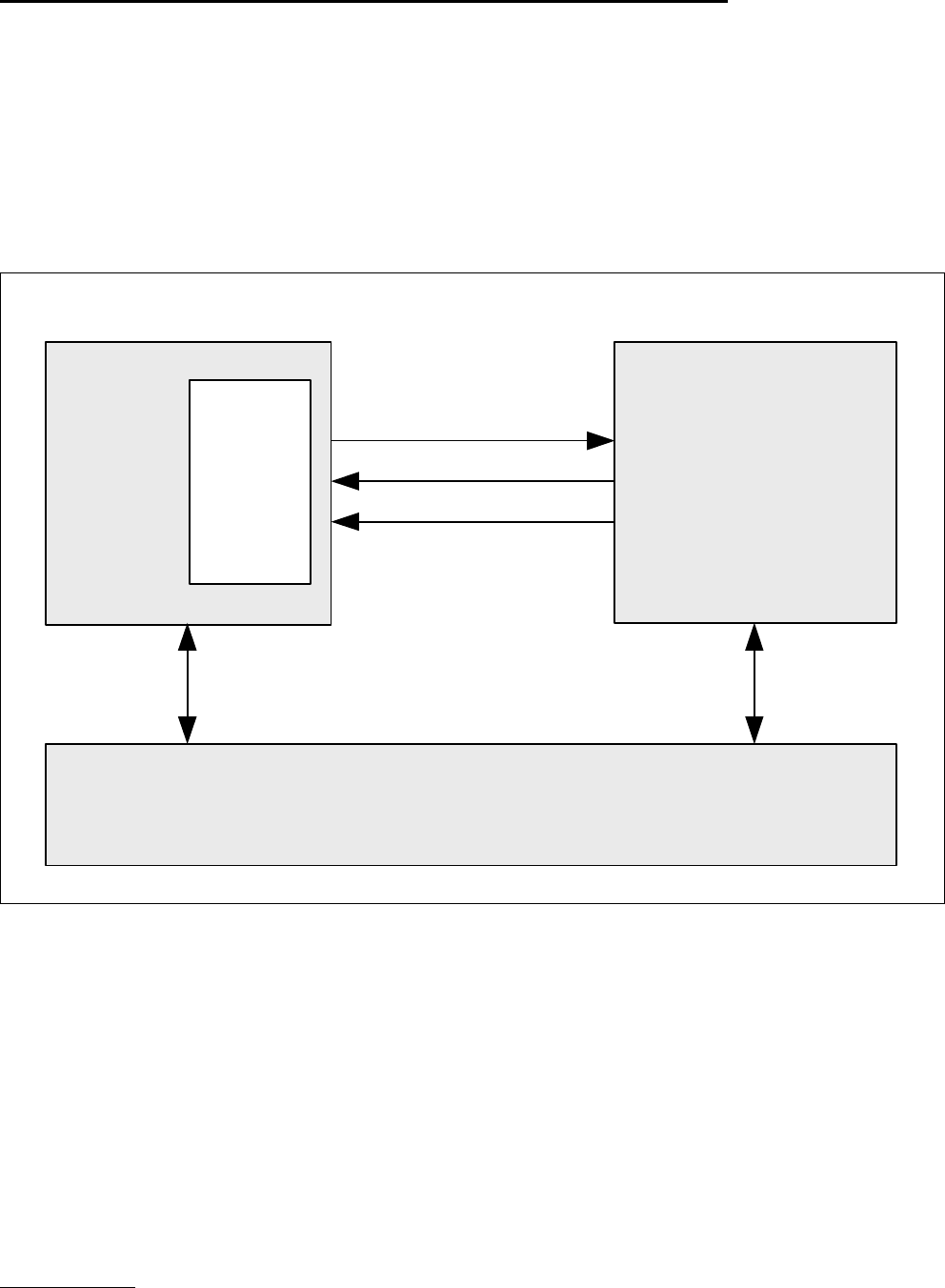
PAN1320-HCI is optimized for a low bill of material (BOM) and a small PCB size. Figure 3 shows a typical
application example.
UARTRTS
UARTTXD
UARTRXD
UARTCTS
ANTENNA
HOST
PCMCLK
PCMFR1
PCMIN
PCMOUT
W
AKEUP
_HOST
WAKEUP
_BT
RESET #
CLK32
PAN
1320-
HCI-BT2.1
TX_CONF
RF_
ACTIVE
SLOT
_STATE
WLAN
Subsystem
Figure 3 Example of a Bluetooth System
Power
Supply
Optional
Bluet
oot
h_Syst
em
_Example.
vsd
The UART interface is used for Bluetooth HCI
communication
between the host and PAN1320-HCI. When the HCI
UART transport layer is used, four interface lines are needed: two for data (UARTTXD and UARTRXD) and two
for hardware flow control (UARTRTS and UARTCTS). When the HCI Three-Wire UART transport layer is used the
hardware flow control lines are optional. In addition to the standard Bluetooth HCI commands, PAN1320-HCI
supports a set of Infineon specific commands called HCI+.
Digital audio can either be sent over the HCI interface or over the dedicated PCM/I2S interface. The PCM/I2S
interface is highly configurable.

PAN1320-HCI-BT2.1
ENW89814A2MF
CONFIDENTIAL
General Device Overview
Product Overview
13
Revision 1.2, 2010-08-18
Low power mode control of PAN1320-HCI and the host can be implemented in different ways, either using the
dedicated WAKEUP_HOST and WAKEUP_BT signals or using signaling over the HCI interface. The host can
reset PAN1320-HCI via the RESET# signal.
A low power clock can be connected to CLK32 or generated internally by a low power oscillator. Power is supplied
to a single VSUPPLY input from which internal regulators can generate all required voltages. The UART and the
PCM interfaces have separate supply voltages so that they can comply with host signaling.
If a WLAN subsystem is collocated with PAN1320-HCI the WLAN coexistence interface should be used to
enhance Bluetooth and WLAN performance. To coexist with external WLAN devices PAN1320-HCI supports
adaptive frequency hopping.
1.6 FW version
PAN1320-HCI is available in different versions. Please check corresponding release documents for latest
information.

Product Overview
14
Revision 1.2, 2010-08-18
PAN1320-HCI-BT2.1
ENW89814A2MF
CONFIDENTIAL Basic Operating Information
2 Basic Operating Information
2.1 Power Supply
PAN1320-HCI is supplied from a single supply voltage VSUPPLY. This supply voltage must always be present.
The PAN1320-HCI chip is supplied from an internally generated 2.5 V supply voltage. This voltage can be
accessed from the VREG pin. This voltage may not be used for supplying other components in the host system
but can be used for referencing the host interfaces.
The PCM interface and the UART interface are supplied with dedicated, independent, reference levels via the
VDDPCM and VDDUART pins. All other digital I/O pins are supplied internally by either 2.5 V (Internal2) or 1.5
V(Internal1). Section 1.4 provides a mapping between pins and supply voltages.
The I/O power domains (VDDPCM and VDDUART) are completely separated from the other power domains and
can stay present also in low power modes.
2.2 Clocking
PAN1320-HCI has one clock input CLK32 that is optional. If used this 32.768 kHz clock must always be present
to assist PAN1320-HCI to keep the time in low power modes.
The low power clock can be generated internally by the crystal oscillator and/or the low power oscillator or provided
externally.
Product Overview
15
Revision 1.2, 2010-08-18
PAN1320-HCI-BT2.1
ENW89814A2MF
CONFIDENTIAL
Interfaces
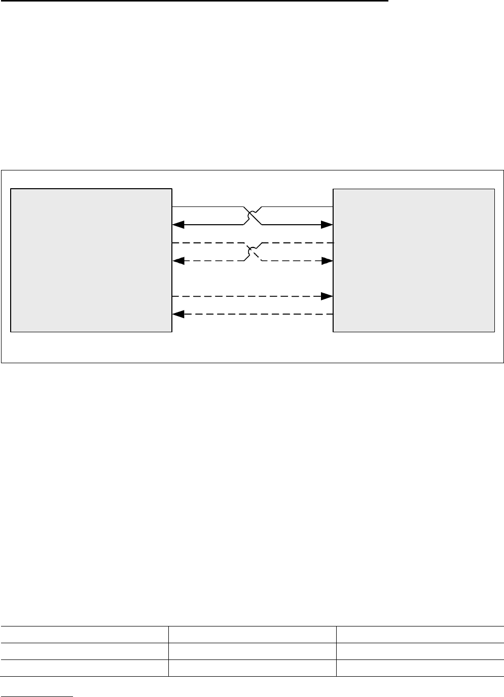
3 Interfaces
3.1 HCI / UART Interface
The HCI/UART interface is the main communication interface between the host and PAN1320-HCI. The standard
HCI commands are supported together with an Infineon-specific set of commands called HCI+.
The interface consists of four UART signals and two wake-up signals as shown in Figure 4. Depending on which
HCI transport layer that is used, some or all of the signals are needed.
UARTTXD
UARTRXD
UARTRTS
UARTCTS
WAKEUP_BT
WAKEUP_HOST
UARTTXD
UARTRXD
UARTRTS
UARTCTS
WAKEUP_BT
WAKEUP_HOST
HCI_UART_Interface.vsd
Figure 4 HCI/UART Interface
3.1.1 Supported Transport Layers
PAN1320-HCI supports the HCI Three-Wire UART transport layer and two derivatives of the HCI UART transport
layer (HCI UART-4W and HCI UART-6W) where the only difference is how low power modes are handled.
PAN1320-HCI automatically detects which transport layer that is used by the host.
3.1.2 UART
The on-chip UART (Universal Asynchronous Receiver and Transmitter) is compatible with standard UARTs and
is optimized for Bluetooth communication. Hardware support for SLIP1) framing and 16-bit CRC calculation
enhances performance with the HCI Three-Wire UART transport layer. A separate supply voltage, VDDUART,
makes it easy to connect the UART interface to any system.
3.1.2.1 Baud Rates
The supported baud rates are listed in Table 2 together with the small deviation error that results from the internal
clock generation. The default baud rate is 115200 Baud.
Table 2 UART Baud Rates
Wanted Baud Rate
Real Baud Rate
Deviation Error (%)
9600
9615
0.16
19200
19230
0.16
1) See http://www.ietf.org/rfc/rfc1055.txt for information about SLIP.

Product Overview
16
Revision 1.2, 2010-08-18
PAN1320-HCI-BT2.1
ENW89814A2MF
CONFIDENTIAL
Interfaces
Table 2 UART Baud Rates (cont’d)
Wanted Baud Rate
Real Baud Rate
Deviation Error (%)
38400
38461
0.16
57600
57522
-0.14
115200
115044
-0.14
230400
230088
-0.14
460800
464285
0.76
921600
928571
0.76
1843200
1857142
0.76
3250000
3250000
0
Product Overview
17
Revision 1.2, 2010-08-18
PAN1320-HCI-BT2.1
ENW89814A2MF
CONFIDENTIAL
F
rame Signal Length
Channel 2 Start Position
3.2 PCM Interface
The PCM interface is used to exchange synchronous data (usually audio) between PAN1320-HCI and the host as
well as to connect e.g. an external audio codec or an external DSP to PAN1320-HCI. It can be configured as an
industry standard PCM interface supporting long and short frame synchronization, as an I2S interface or as an
IOM-2 interface in terminal mode with reduced capabilities.
The main features of the PCM interface are:
• Two bidirectional PCM channels
• Separate supply voltage (VDDPCM) for easy interfacing to other systems
• Support of 16-bit linear samples and 8-bit A-law/μ-law compressed samples as defined in the Bluetooth
specification
• 8 x 32-bit FIFOs for each channel
• Programmable frame length
• Programmable frame signal length
• Programmable channel start positions
• Programmable idle level on PCMOUT
• Programmable low-power/inactive levels on all PCM pins
• Data word LSB justified or MSB justified with respect to frame signal
• Clock master/slave mode
• Frame master/slave mode
• Fractional divider for PCM clock generation
3.2.1 Overview
The PCM interface consists of five signals as shown in Figure 5 below.
PCMCLK
M L M L M
PCMOUT S 1 1 1 1 1 9 8 7 6 5 4 3 2 1 S IDLE S 1 1 1 1 1 9 8 7 6 5 4 3 2 1 S IDLE S 1 1 1
B 4 3 2 1 0 B B 4 3 2 1 0 B B 4 3 2
M L M L M
PCMIN S 1 1 1 1 1 9 8 7 6 5 4 3 2 1 S Don’t Care S 1 1 1 1 1 9 8 7 6 5 4 3 2 1 S Don’t Care S 1 1 1
B 4 3 2 1 0 B B 4 3 2 1 0 B B 4 3 2
PCMFR 1
Data Word Length
F
rame
Length
Figure 5 PCM_Signals_Overview
PCM_Interface_
PCM_
Signals_Overview.vsd
The clock signal PCMCLK is the timing base for the other signals in the PCM interface. In clock master mode,
PAN1320-HCI generates PCMCLK from the internal system clock using a fractional divider. In clock slave mode
PCMCLK is an input to PAN1320-HCI and has to be supplied by an external source. The maximum PCMCLK
frequency (in both modes) is 1/8 of the internal system clock frequency.
The PCM interface supports up to two bidirectional channels. Data is transmitted on PCMOUT and received on
PCMIN, always with the most significant bit first. 16-bit linear audio samples and 8-bit A-law or μ-law compressed
audio samples are supported.
The samples are organized in frames such that each frame contains one sample in each direction of each active
channel. The frame rate (i.e. sample rate) is controlled by the PCMCLK frequency and the programmable Frame
Length. In the firmware the sample rate has been fixed to 8 kHz. This means that the PCMCLK frequency can be
calculated from Frame Length and does not have to be specified.

Product Overview
18
Revision 1.2, 2010-08-18
PAN1320-HCI-BT2.1
ENW89814A2MF
CONFIDENTIAL
Each channel has its own frame signal (PCMFR1/PCMFR2) that indicates where in the frame the channel starts.
The Frame Signal Length is programmable. The start position of PCMFR2 in the frame is also programmable
(Channel 2 Start Position). PCMFR1 always starts at the beginning of the frame.
In frame master mode, PAN1320-HCI generates PCMFR1 and PCMFR2. In frame slave mode the signal
PCMFR1 is an input to PAN1320-HCI and has to be supplied externally. PCMFR2 is still generated by PAN1320-
HCI. When only one channel is used PCMFR2 can be switched off with the HCI command
HCI_Infineon_Write_PCM_Mode.
In PAN1320-HCI the second PCM channel cannot be used. The on-module bluetooth controller can handle two
PCM channels but due to restrictions in the controller pinout the second PCM channel cannot be supported when
using EEPROM.
Product Overview
19
Revision 1.2, 2010-08-18
PAN1320-HCI-BT2.1
ENW89814A2MF
CONFIDENTIAL
Co n tro l
Un it
3.3 WLAN Coexistence Interface
PAN1320-HCI has a WLAN coexistence interface that is based on the IEEE 802.15.2 Packet Traffic Arbitration
(PTA) scheme2). The interface prevents interference between collocated WLAN and Bluetooth devices by not
letting the two devices transmit and/or receive at the same time. WLAN packets and Bluetooth packets are
assigned priorities, and a control unit decides on a per-packet basis which of the devices that should be allowed
to operate.
The interface uses three wires as shown in Figure 6.
Host PAN1320-HCI-BT2.1
TX_CONF
SLOT_STATE
RF_ACTIVE
Host
WLAN_Coexistence_Interface_2 .1.vsd
Figure 6 WLAN Coexistence Interface
2) “802.15.2: Coexistence of Wireless Personal Area Networks with other Wireless Devices Operating in Unlicensed
Frequency Bands”, IEEE, 28 August 2003

PAN1320-HCI-BT2.1
ENW89814A2MF
CONFIDENTIAL
General Device Capabilities
Product Overview
20
Revision 1.2, 2010-08-18
4 General Device Capabilities
4.1 HCI+ and Bluetooth Device Data (BD_DATA)
In addition to the standard Bluetooth HCI commands and events,
PAN1320-HCI
supports a set of Infineon-specific
commands and events called HCI+. All Infineon-specific features are accessed using HCI+.
All configuration information that is critical for correct operation of PAN1320-HCI is called Bluetooth Device Data
(BD_DATA). This data is stored in the module’s EEPROM and is initialized during module manufacturing.
BD_DATA can be read and written with the HCI+ commands Infineon_Read_BD_Data and
Infineon_Write_BD_Data.
Note:
Each PAN1320-HCI module is delivered with a unique Bluetooth device address in it’s BD_DATA. This
information should not be changed!
4.2 Manufacturer Mode
HCI+ commands that modify critical information are not available during normal operation. To access these
commands the host must first tell PAN1320-HCI to enter manufacturer mode with the
Infineon_Manufacturer_Mode
command.
Operations that are only allowed in manufacturer mode are for example:
• Changing the Baud rate with Infineon_Set_UART_Baudrate.
• Accessing Bluetooth Device Data (BD_DATA) with any of the following commands:
Infineon_Write_BD_Data,
Infineon_Read_BD_Data,
Infineon_Write_Ext_EEPROM_Data,
Infineon_Read_Ext_EEPROM_Data.
• Accessing internal memory and registers with
Infineon_Memory_Write and Infineon_Memory_Read.
It is necessary to leave manufacturer mode before start of normal operation. Leaving manufacturer mode is done
with the
Infineon_Manufacturer_Mode
command.
4.3 Firmware ROM Patching
4.3.1 Patch Support
PAN1320-HCI contains dedicated hardware that makes it possible to apply patches to any code and data in the
firmware ROM. The hardware is capable of replacing up to 32 blocks of 16 bytes each with new content. In addition
to this, an 8 kByte area of the firmware RAM has been reserved for patches. This area can be filled with any
combination of code and data.

Product Overview
21
Revision 1.2, 2010-08-18
PAN1320-HCI-BT2.1
ENW89814A2MF
CONFIDENTIAL
Bluetooth Capabilities
5 Bluetooth Capabilities
5.1 Supported Features
PAN1320-HCI supports all new core features in the Bluetooth 2.1 + EDR specification, including:
• Enhanced Data Rate up to 3 Mbit/s
• Adaptive Frequency Hopping (AFH)
• All packet types
• All LMP features except those related to the features listed in Chapter 5.2
• Authentication, Pairing and Encryption
• Secure Simple Pairing
• Sniff Subrating
• Extended Inquiry Response
• Quality of Service
• Channel Quality Driven Data Rate change
• Sniff, Hold
• Role Switch
• RSSI and Power Control
• Power class 2 and 3
• 7 point-to-multipoint connections
• Scatternet with two slave roles while still being discoverable
• 2 synchronous links (SCO/eSCO)
• A-law, μ-law, CVSD and transparent synchronous data
• Dual SCO/eSCO channels in scatternet
5.2 Not-supported Features
• Park State
• Master Link Key
• Broadcast
5.3 PAN1320-HCI Specifics and Extensions
5.3.1 During Connection
5.3.1.1 Scatternet and Piconet Capabilities
PAN1320-HCI supports point-to-multipoint and scatternet scenarios:
• Up to 7 links
• Up to 2 simultaneous slave roles
• Always capable of responding to inquiry and remote name request
• Always capable of Inquiry

Product Overview
22
Revision 1.2, 2010-08-18
PAN1320-HCI-BT2.1
ENW89814A2MF
CONFIDENTIAL
Bluetooth Capabilities
5.3.1.2 Role Switch
Only one role switch can be performed at a time. If a role switch request is pending, other role switch requests on
the same or other links are rejected. If a role switch fails, PAN1320-HCI will automatically try again a maximum of
three times. Encryption (if present) is stopped in the old piconet before a role switch is performed and re-enabled
when the role switch has succeeded or failed. If the Bluetooth 2.1 introduced feature “pause encryption” is enabled
in PAN1320-HCI and supported in the remote device, the the encryption will instead be paused before the role
switch and resumed after the role switch which leads to an atomic encryption of data throughout the role switch.
If the physical link is in Sniff Mode or Hold Mode, or has any synchronous logical transports, a role switch will not
be performed.
5.3.1.3 Dynamic Polling Strategy
In addition to the regular polling scheme, PAN1320-HCI dynamically assigns unused slots to links where data is
exchanged. This adapts very well to bursty traffic and improves throughput and latency on the links.
5.3.1.4 Adaptive Frequency Hopping (AFH)
PAN1320-HCI supports adaptive frequency hopping according to the Bluetooth 2.1 + EDR specification. AFH
switch and channel classification are supported both as master and slave. Channel classification from the host is
also supported.
A number of HCI+ commands and events are available to provide information about AFH operation. The
commands Infineon_Enable_AFH_Info_Sending and Infineon_Disable_AFH_Info_Sending turn on and off the
Infineon_AFH_Info events that provide detailed information about channel classification, channel maps,
interferers, etc.
If enabled by the Infineon_Enable_Infineon_Events command, the Infineon_AFH_Extraordinary_RSSI event
informs the host whenever extraordinary RSSI measurements in unused slots have been started. This is done
when the number of known good channels has
decreased
below a critical limit and
periodically
after a defined time.
The Infineon_Set_AFH_Measurement_Period command can be used to configure the duration of the AFH
measurement period.
5.3.1.5 Channel Quality Driven Data Rate Change (CQDDR)
PAN1320-HCI supports channel quality driven data rate change according to the Bluetooth 2.1 + EDR
specification. A device that receives an LMP_preferred_rate message is not required to follow all
recommendations. PAN1320-HCI normally at least follows the recommendation whether to use forward error
correction (FEC) or not. If possible,
recommendations
about packet size and modulation scheme will be taken into
account. When PAN1320-HCI sends an LMP_preferred_rate to another device the proposal always includes
preferences for all parameters.
The HCI+ commands
Infineon_Enable_CQDDR_Info_Sending
and
Infineon_Disable_CQDDR_Info_Sending
turn
on and off sending of the Infineon_CQDDR_Info event. This event provides information to the host every time a
new CQDDR proposal is sent to a remote device.
The link keys are stored in the module’s EEPROM.
5.3.2 Synchronous Links
PAN1320-HCI supports up to two simultaneous synchronous links (SCO/eSCO).
5.3.2.1 Interface
The interface for synchronous data is either the HCI transport layer or the dedicated PCM/I2S interface. The
choice of interface for a synchronous connection is done with the HCI+ command

Product Overview
23
Revision 1.2, 2010-08-18
PAN1320-HCI-BT2.1
ENW89814A2MF
CONFIDENTIAL
Bluetooth Capabilities
Infineon_Config_Synchronous_Interface and must be done before the connection is established. The default
interface is configurable via the bit Default_SCO_interface in the BD_DATA parameter BB_Conf.
All details about the PCM/I2S interface are described in Section 3.2.

Product Overview
24
Revision 1.2, 2010-08-18
PAN1320-HCI-BT2.1
ENW89814A2MF
CONFIDENTIAL
Bluetooth Capabilities
5.3.2.2 Voice Coding
Table 3 shows the supported values of the Bluetooth parameter Voice_Settings.
Table 3 Supported Voice Settings
Parameter
Supported Values
Input Coding
Linear (PCM/I2S only), μ-law, A-law
Input Data Format
2’s complement
Input Sample Size
16-bit (only relevant for linear input coding)
Air Coding Format
CVSD, μ-law, A-law, Transparent Data
Linear_PCM_Bit_Pos
Not used. Please see the parameter Channel_Pos in the
Infineon_Write_PCM_Mode
command for similar functionality.
PAN1320-HCI supports transcoding between any combination of linear, μ-law and A-law. If the air coding format
is “Transparent Data” and the synchronous interface is the transport layer, the input coding is ignored. If
transparent data is sent through the PCM/I2S interface, the input coding determines if 8-bit or 16-bit samples are
used. Transparent Data is the only setting for which data rates other than 64 kbit/s can be used.
5.3.3 RSSI and Output Power Control
5.3.3.1 Received Signal Strength Indication (RSSI)
PAN1320-HCI supports received signal strength measurements and uses LMP signaling to keep the output power
of a remote device within the golden receive power range. The range is set with the BD_DATA parameters
RSSI_Min and RSSI_Max.
5.3.3.2 Output Power Control
PAN1320-HCI supports power control according to the Bluetooth 2.1+EDR specification.
• The output power can be controlled in up to 4 configurable steps. PAN1320-HCI can work as a class 2 or 3
device, depending on the settings.
• Fine tuning can be used on the power steps.
• A default sub-state power step can be set
The power step configuration is set through BD_DATA parameters.
The Inquiry output power can be programmed with the Write Inquiry Transmit Power Level command introduced
in the 2.1 Bluetooth Core specification.
5.3.3.3 Ultra Low Transmit Power
For high security devices the output power can be reduced to a value that reduces the communication range to a
few inches. This mode is enabled with the HCI+ command Infineon_TX_Power_Config.

Product Overview
25
Revision 1.2, 2010-08-18
PAN1320-HCI-BT2.1
ENW89814A2MF
CONFIDENTIAL
Electrical Characteristics
6
Electrical Characteristics
6.1 Absolute Maximum Ratings
Table 4 Absolute Maximum Ratings
Parameter
Symbol
Values
Unit
Note / Test Condition
Min.
Typ.
Max.
Storage temperature
-40
–
125
°C
–
VSUPPLY supply voltage
-0.3
–
6.0
V
–
VDDUART supply voltage
-0.9
–
4.0
V
–
VDDPCM supply voltage
-0.9
–
4.0
V
–
VREG
-0.3
–
4.0
V
VSUPPLY > 4 V
VREG
-0.3
–
VSUPPLY
V
VSUPPLY < 4 V
ONOFF
-0.3
–
VSUPPLY+0.3
V
Input voltage range
-0.9
–
4.0
V
–
Output voltage range
-0.9
–
4.0
V
-9
ESD
–
–
1.0
kV
According to MIL-STD883D
method 3015.7
Note:
Stresses above those listed here are likely to cause permanent damage to the device. Exposure to absolute
maximum rating conditions for extended periods may affect device reliability.
Maximum ratings are absolute ratings; exceeding only one of these values may cause irreversible damage
to the integrated circuit.
Maximum ratings are not operating conditions.
6.2 Operating Conditions
Table 5 Operating Conditions
Parameter
Symbol
Values
Unit
Note / Test Condition
Min.
Typ.
Max.
Operating temperature
-40
–
85
°C
–
Main supply voltage (Vsupply)
2.9
–
4.1
V
–
VDDUART
1.35
–
3.6
V
–
VDDPCM
1.35
–
3.6
V
–

Product Overview
26
Revision 1.2, 2010-08-18
PAN1320-HCI-BT2.1
ENW89814A2MF
CONFIDENTIAL
Electrical Characteristics
6.3 DC Characteristics
6.3.1 Pad Driver and Input Stages
For more information, see Chapter 1.4.
Table 6 Internal1 (1.5 V) Supplied Pins
Parameter
Symbol
Values
Unit
Note / Test Condition
Min.
Typ.
Max.
Input low voltage
-0.3
–
0.27
V
–
Input high voltage
1.15
–
3.6
V
–
Output low voltage
–
–
0.25
V
IOL = 1 mA
Output high voltage
1.1
–
–
V
IOH = -1 mA
Continuous
Load
1)
–
–
1
mA
–
Pin Capacitance
–
–
10
pF
–
Magnitude Pin Leakage
–
0.01
1
μ
A
Input and output drivers
disabled
1) The totaled continuous load for all Internal1 supplied pins shall not exceed 2mA at the same time
Table 7 Internal2 (2.5 V) Supplied Pins
Parameter
Symbol
Values
Unit
Note / Test Condition
Min.
Typ.
Max.
Input low voltage
-0.3
–
0.45
V
–
Input high voltage
1.93
–
2.8
V
P0.10
Input high voltage
1.93
–
3.6
V
Other pins
Output low voltage
–
–
0.25
V
IOL = 5 mA
Output low voltage
–
–
0.15
V
IOL = 2 mA
Output high voltage
2.0
–
–
V
IOH = -5 mA
Output high voltage
2.1
–
–
V
IOH = -2 mA
Continuous
Load
1)
–
–
5
mA
–
Pin Capacitance
–
–
10
pF
–
Magnitude Pin Leakage
–
0.01
1
μ
A
Input and output drivers
disabled
1) The totaled continuous load for all Internal2 supplied pins shall not exceed 35 mA at the same time
Table 8 VDDUART Supplied Pins
Parameter
Symbol
Values
Unit
Note / Test Condition
Min.
Typ.
Max.
Input low voltage
-0.3
–
0.2*VDDUART
V
–
Input high voltage
0.7*VDDUART
–
VDDUART+0.3
V
P0.5/UARTRXD
Input high voltage
0.7*VDDUART
–
3.6
V
Other pins

Product Overview
27
Revision 1.2, 2010-08-18
PAN1320-HCI-BT2.1
ENW89814A2MF
CONFIDENTIAL
Electrical Characteristics
Table 8 VDDUART Supplied Pins (cont’d)
Parameter
Symbol
Values
Unit
Note / Test Condition
Min.
Typ.
Max.
Output low voltage
–
–
0.25
V
IOL = 5 mA
VDDUART = 2.5 V
Output low voltage
–
–
0.15
V
IOL = 2 mA
VDDUART = 2.5 V
Output high voltage
VDDUART
-0.25
–
–
V
IOH = -5 mA
VDDUART = 2.5 V
Output high voltage
VDDUART
-0.15
–
–
V
IOH = -2 mA
VDDUART = 2.5 V
Continuous
Load
1)
–
–
5
mA
–
Pin Capacitance
–
–
10
pF
–
Magnitude Pin Leakage
–
0.01
1
μ
A
Input and output drivers
disabled
1) The totaled continuous load for all VDDUART supplied pins shall not exceed 35 mA at the same time
Table 9 VDDPCM Supplied Pins
Parameter
Symbol
Values
Unit
Note / Test Condition
Min.
Typ.
Max.
Input low voltage
-0.3
–
0.2*VDDPCM
V
–
Input high voltage
0.7*VDDPCM
–
3.6
V
–
Output low voltage
–
–
0.25
V
IOL = 5 mA
VDDPCM = 2.5 V
Output low voltage
–
–
0.15
V
IOL = 2 mA
VDDPCM = 2.5 V
Output high voltage
VDDPCM
-0.25
–
–
V
IOH = -5 mA
VDDPCM = 2.5 V
Output high voltage
VDDPCM
-0.15
–
–
V
IOH = -2 mA
VDDPCM = 2.5 V
Continuous
Load
1)
–
–
5
mA
–
Pin Capacitance
–
–
10
pF
–
Magnitude Pin Leakage
–
0.01
1
μ
A
Input and output drivers
disabled
1) The totaled continuous load for all VDDPCM supplied pins shall not exceed 35 mA at the same time
Table 10 ONOFF PIN
Parameter
Symbol
Values
Unit
Note / Test Condition
Min.
Typ.
Max.
Input low voltage
–
–
0.7
V
–
Input high voltage
1.7
–
VSUPPLY
V
–
Input current
-1
0.01
1
μ
A
ONOFF = 0 V

Product Overview
28
Revision 1.2, 2010-08-18
PAN1320-HCI-BT2.1
ENW89814A2MF
CONFIDENTIAL
Electrical Characteristics
6.3.2 Pull-ups and Pull-downs
Table 11 Pull-up and Pull-down Currents
Pin
Pull Up Current
Pull Down Current
Unit
Conditions
Min.
Typ.
Max.
Min.
Typ.
Max.
P0.12/SDA0,
P0.13/SCL0
260
740
1300
N/A
N/A
N/A
μ
A
Pull-up current
measured with
pin voltage = 0 V
Pull-down current
measured with
pin voltage =
supply voltage
Min
measured
at
125°C
with supply = 1.35 V
Typ. measured at 27°C
with supply = 2.5V
Max measured at
-40°C with
supply = 3.63 V
TRST#, JTAG#,
P0.0/PCMFR1,
P0.1/PCMCLK,
P0.2/PCMIN,
P0.3/PCMOUT
22
130
350
23
150
380
μ
A
P0.4/UARTTXD,
P0.5/UARTRXD,
P0.6/UARTRTS,
P0.7/UARTCTS,
P0.10/PSEL1,
P0.8/PAON,
P0.9/PSEL0,
P0.11/RXON,
P0.14/TX_CONF,
P0.15/SLEEPX
4.2
24
68
3.0
20
55
μ
A
P1.0/TMS,
P1.1/TCK,
P1.2/TDI,
P1.3/TDO,
P1.4/RTCK,
P1.5/CLK32,
P1.6,
P1.7/WAKEUP_BT,
P1.8/WAKEUP_HOST,
1.1
6.0
17
0.75
5.0
14
μ
A
6.3.3 Protection Circuits
All pins have an inverse protection diode against VSS.
P0.10 has an inverse diode against Internal2.
P0.5/UARTRXD has an inverse diode against VDDUART.
All other pins have no diode against their supply.

Product Overview
29
Revision 1.2, 2010-08-18
PAN1320-HCI-BT2.1
ENW89814A2MF
CONFIDENTIAL
Electrical Characteristics
6.3.4 System Power Consumption
The following table shows the Vsupply current consumption. All I/O currents are neglected since they depend
mainly on the external load. T = 25°C, Output Power = 0 dBm
Table 12 Current Consumption in Different Operating Modes
Parameter
Symbol
Values
Unit
Note / Test Condition
Min.
Typ.
Max.
Ultra Low Power Mode
–
170
–
μ
A
–
Page & Inquiry Scan (1.28 s)
–
1.1
–
mA
–
Sniff (1.28 s)
–
0.35
–
mA
–
ACL (Transmit DH1)
–
38
–
mA
Basic Rate, 179.2 kbit/s1)
ACL (Receive DH1)
–
35
–
mA
Basic Rate, 179.2 kbit/s
ACL (Transmit 2-DH1)
–
40
–
mA
Enhanced Data Rate, 358.4 kbit/s1)
ACL (Receive 2-DH1)
–
37
–
mA
Enhanced Data Rate, 358.4 kbit/s1)
ACL (Transmit 3-DH1)
–
40
–
mA
Enhanced Data Rate, 544.0 kbit/s1)
ACL (Receive 3-DH1)
–
37
–
mA
Enhanced Data Rate, 544.0 kbit/s1)
SCO (HV3)
–
19
–
mA
–
eSCO (Symmetric 64 kbit/s, EV3)
–
20
–
mA
–
eSCO (Symmetric 64 kbit/s, 2-EV3)
–
13
–
mA
Enhanced Data Rate
eSCO (Symmetric 64 kbit/s, 3-EV3)
–
11
–
mA
Enhanced Data Rate
eSCO (Symmetric 64 kbit/s, EV5)
–
14
–
mA
–
eSCO (Symmetric 64 kbit/s, 2-EV5)
–
10
–
mA
Enhanced Data Rate
eSCO (Symmetric 64 kbit/s, 3-EV5)
–
8.7
–
mA
Enhanced Data Rate
1) Figure indicates maximum possible data rate with this packet type
I/O currents are not included since they depend mainly on external loads.
Table 13 Max. Load at the Different Supply Voltages
Parameter
Symbol
Values
Unit
Note / Test Condition
Min.
Typ.
Max.
Vsupply
–
–
100
mA
Peak current
6.4 AC Characteristics
Table 14 PCM Interface Timing
Parameter
Symbol
Values
Unit
Note / Test Condition
Min.
Typ.
Max.
PCMOUT delay from rising clock edge
t
d1
–
–
100
ns
PCMFRy setup time to falling clock edge
t
s1
100
1)
–
–
ns
PCMFRy hold time from falling clock edge
t
h1
100
1)
–
–
ns

PAN1320-HCI-BT2.1
ENW89814A2MF
CONFIDENTIAL
Electrical Characteristics
Product Overview
30
Revision 1.2, 2010-08-18
Table 14 PCM Interface Timing (cont’d)
Parameter
Symbol
Values
Unit
Note / Test Condition
Min.
Typ.
Max.
PCMIN setup time to falling clock edge
t
s2
50
–
–
ns
PCMIN hold time from falling clock edge
t
h2
50
–
–
ns
1) In frame slave mode
Table 15 Timing Characteristics of PCM Interface for the First Bit
Parameter
Symbol
Values
Unit
Note /
Test Condition
Min.
Typ.
Max.
PCMOUT delay from PCMCLK or PCMFR1
t
d1
–
–
100
ns
PCMFR1 delay from PCMCLK
t
d2
-0.25
T
1)
–
+0.25 T
ns
1) T is the PCMCLK period time
6.4.1 Characteristics of 32.768 kHz Clock Signal
The 32.768 kHz clock signal applied to CLK32 must be a rectangular waveform with a duty cycle of between 10%
and 90%. The frequency accuracy must be better than 250 ppm. The rise and fall time of the signal must be less
than 10
μ
s.
6.5 RF Part
6.5.1 Characteristics RF Part
The
characteristics
involve the spread of values to be within the specific
temperature
range. Typical characteristics
are the median of the production.
All values refers to Infineon reference design. All values will be updated after verification/Characterisation.
6.5.1.1 Bluetooth Related Specifications
Table 16 BDR - Transmitter Part
Parameter
Symbol
Values
Unit
Note / Test Condition
Min.
Typ.
Max.
Output power (high gain)
0.5
2.5
4.5
dBm
Default settings
Output power (highest gain)
–
4.5
–
dBm
Maximum settings
Power control step size
4
6
8
dB
–
Frequency range fL
2400
2401.3
–
MHz
–
Frequency range fH
–
2480.7
2483.5
MHz
–
20 dB bandwidth
–
0.930
1
MHz
–
2nd adjacent channel power
–
-40
-20
dBm
–
3rd adjacent channel power
–
-60
-40
dBm
–

PAN1320-HCI-BT2.1
ENW89814A2MF
CONFIDENTIAL
Electrical Characteristics
Product Overview
31
Revision 1.2, 2010-08-18
Table 16 BDR - Transmitter Part (cont’d)
Parameter
Symbol
Values
Unit
Note / Test Condition
Min.
Typ.
Max.
>3rd adjacent channel power
–
-64
-40
dBm
Max. 2 of 3 exceptions @
52 MHz offset might be used
Average modulation deviation
for 00001111 sequence
140
156
175
kHz
–
Minimum modulation deviation
for 01010101 sequence
115
145
–
kHz
–
Ratio Deviation 01010101 /
Deviation 00001111
0.8
1
–
–
Initial carrier frequency
tolerance |foffset|
–
–
75
kHz
–
Carrier frequency drift
(one slot) |fdrift|
–
10
25
kHz
–
Carrier frequency drift
(three slots) |fdrift|
–
10
40
kHz
–
Carrier frequency drift
(five slots) |fdrift|
–
10
40
kHz
–
Carrier frequency driftrate
(one slot) |fdriftrate|
–
5
20
kHz/50 ms
–
Carrier frequency driftrate
(three slots) |fdriftrate|
–
5
20
kHz/50 ms
–
Carrier frequency driftrate
(five slots) |fdriftrate|
–
5
20
kHz/50 ms
–
Table 17 BDR -Receiver Part
Parameter
Symbol
Values
Unit
Note / Test Condition
Min.
Typ.
Max.
Sensitivity
–
-86
-81
dBm
Ideal wanted signal
C/I-performance:
-4th adjacent channel
–
-51
-40
dB
–
C/I-performance:
-3rd adjacent channel
(1st adj. of image)
–
-46
-20
dB
–
C/I-performance:
-2nd adjacent channel (image)
–
-35
-9
dB
–
C/I-performance:
-1st adjacent channel
–
-4
0
dB
–
C/I-performance: co. channel
–
9
11
dB
–
C/I-performance:
+1st adjacent channel
–
-4
0
dB
–
C/I-performance:
+2nd adjacent channel
–
-40
-30
dB
–

PAN1320-HCI-BT2.1
ENW89814A2MF
CONFIDENTIAL
Electrical Characteristics
Product Overview
32
Revision 1.2, 2010-08-18
Table 17 BDR -Receiver Part (cont’d)
Parameter
Symbol
Values
Unit
Note / Test Condition
Min.
Typ.
Max.
C/I-performance:
+3rd adjacent channel
–
-50
-40
dB
–
Blocking performance
30 MHz - 2 GHz
10
–
–
dBm
Some spurious responses, but
according to BT-specification
Blocking performance
2 GHz - 2.4 GHz
-27
–
–
dBm
–
Blocking performance
2.5 GHz - 3 GHz
-27
–
–
dBm
–
Blocking performance
3 GHz - 12.75 GHz
10
–
–
dBm
Some spurious responses, but
according to BT-specification
Intermodulation performance
-39
-34
–
dBm
Valid for all intermodulation tests
Maximum input level
-20
–
–
dBm
–
Table 18 EDR - Transmitter Part
Parameter
Symbol
Values
Unit
Note / Test Condition
Min.
Typ.
Max.
Output power (high gain)
-2.5
–
2
dBm
Relative transmit power:
PxPSK - PGFSK
-4
-0.6
1
dB
Carrier frequency stability
|
ω
i|
–
–
75
kHz
–
Carrier frequency stability
|
ω
i+
ω
0|
–
–
75
kHz
–
Carrier frequency stability
|
ω
0|
–
2
10
kHz
–
DPSK - RMS DEVM
–
10
20
%
–
8DPSK - RMS DEVM
–
10
13
%
–
DPSK - Peak DEVM
–
20
35
%
–
8DPSK - Peak DEVM
–
20
25
%
–
DPSK - 99% DEVM
–
–
30
%
–
8DPSK - 99% DEVM
–
–
20
%
–
Differential phase encoding
99
100
–
%
–
1st adjacent channel power
–
-40
-26
dBc
–
2nd adjacent channel power
–
–
-20
dBm
Carrier power measured at basic
rate
3rd adjacent channel power
–
–
-40
dBm
Carrier power measured at basic
rate

PAN1320-HCI-BT2.1
ENW89814A2MF
CONFIDENTIAL
Electrical Characteristics
Product Overview
33
Revision 1.2, 2010-08-18
Table 19 EDR -Receiver Part
Parameter
Symbol
Values
Unit
Note / Test Condition
Min.
Typ.
Max.
DQPSK-Sensitivity
–
-88
-83
dBm
Ideal wanted signal
8DPSK-Sensitivityl
–
-83
-77
dBm
Ideal wanted signal
DQPSK - BER Floor Sensitivity
–
-84
-60
dBm
–
8DPSK - BER Floor Sensitivity
–
-79
-60
dBm
–
DQPSK - C/I-performance:
-4th adjacent channel
–
-53
-40
dB
–
DQPSK - C/I-performance:
-3rd adjacent channel (1st adj. of image)
–
-47
-20
dB
–
DQPSK - C/I-performance:
-2nd adjacent channel (image)
–
-31
-7
dB
–
DQPSK - C/I-performance:
-1st adjacent channel
–
-7
0
dB
–
DQPSK - C/I-performance:
co. channel
–
11
13
dB
–
DQPSK - C/I-performance:
+1st adjacent channel
–
-9
0
dB
–
DQPSK - C/I-performance:
+2nd adjacent channel
–
-44
-30
dB
–
DQPSK - C/I-performance:
+3rd adjacent channel
–
-50
-40
dB
–
8DPSK - C/I-performance:
-4th adjacent channel
–
-48
-33
dB
–
8DPSK - C/I-performance:
-3rd adjacent channel (1st adj. of image)
–
-44
-13
dB
–
8DPSK - C/I-performance:
-2nd adjacent channel (image)
–
-25
0
dB
–
8DPSK - C/I-performance:
-1st adjacent channel
–
-5
5
dB
–
8DPSK - C/I-performance:
co. channel
–
17
21
dB
–
8DPSK - C/I-performance:
+1st adjacent channel
–
-5
5
dB
–
8DPSK - C/I-performance:
+2nd adjacent channel
–
-36
-25
dB
–
8DPSK - C/I-performance:
+3rd adjacent channel
–
-46
-33
dB
–
Maximum input level
-20
–
–
dBm
–
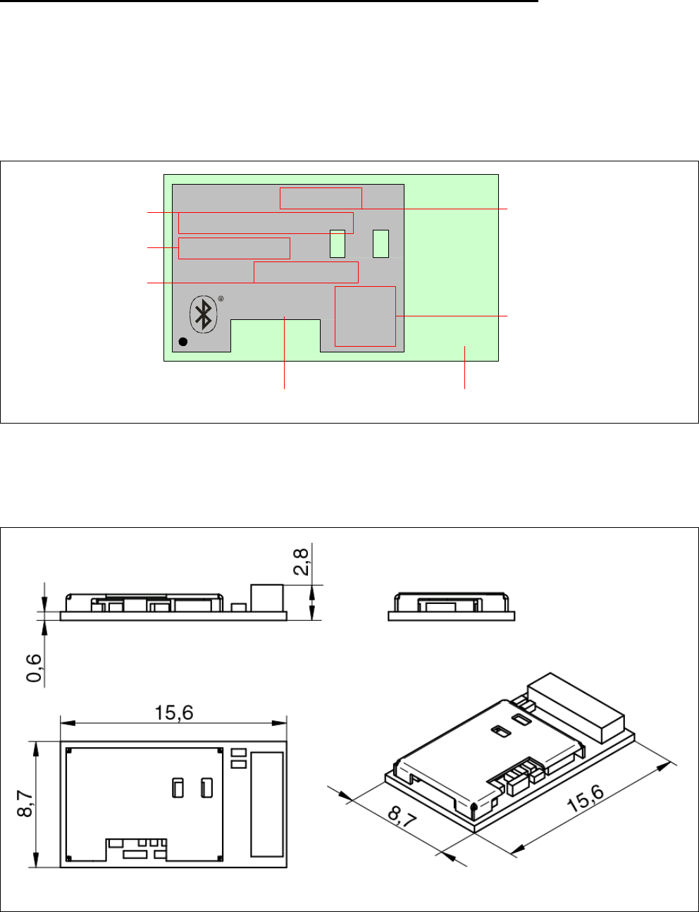
Product Overview
34
Revision 1.2, 2010-08-18
PAN1320-HCI-BT2.1
ENW89814A2MF
CONFIDENTIAL
Package Information
7 Package Information
7.1 Package Marking
Ordering
Code
Date
Code
FCC I
D
PAN1320 HW/SW
ENW89814A2MF
YYWWDLL
FCC ID:T7VEBMU
Case
PCB
Ver
s
ion
HW – Hardware Version
SW – Software Version
Machine
readable
2D bar c
ode
Panasonic usage only ,
could be changed without
any notice
Figure 7 Package Marking
7.2 Production Package
Production
_Package.vsd
Figure 8 Production Package
All dimensions are in mm.
Tolerances on all outer dimensions, height, width and length, are +/- 0.2 mm.
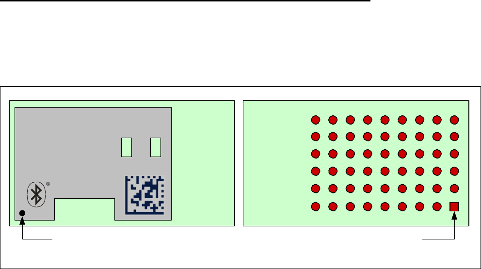
Product Overview
35
Revision 1.2, 2010-08-18
PAN1320-HCI-BT2.1
ENW89814A2MF
CONFIDENTIAL
Package Information
7.2.1 Pin Mark
Pin 1 (A1) is marked on bottom footprint and on the top of the shield on the module according to Figure 9.
Diameter of pin 1 mark on the shield is 0.40 mm.
PAN 1320 12/01
ENW89814A2MF
0902401
FCC ID:T7VEBMU
F9 F8 F7
E9 E8 E7
D9 D8 D7
C9 C8 C7
F6 F5 F4
E6 E5 E4
D6 D5 D4
C6 C5 C4
F3 F2 F1
E3 E2 E1
D3 D2 D1
C3 C2 C1
B9
B8
B7
B6 B5 B4 B3 B2 B1
A9
A8
A7
A6 A5 A4 A3 A2 A1
Pin 1 marking top side Pin 1 marking bottom side
Top_and _Bottom_Views.vsd
Figure 9 Top View and Bottom View
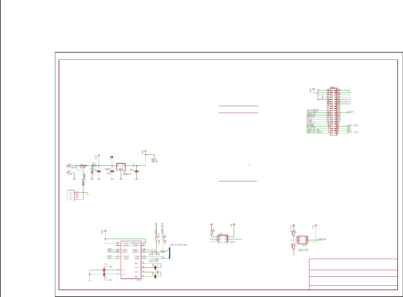
:I:
-
1
i
.
P
l
i
= =
GNOB
c
-
1
c
...
t=
l.
z
::I
u
.!2'
T
c
-
Q)
0
"r"'"LL
l:'i2
1-N
aJ<C
..!."'t
(.)"r"'"
co
,0')
ceo
NS
z
<C
a.
c:
0
E
....
.
c
E
:
c:
0
:;:::;
C
u
'il
<
(
c:
co
r-
co
0
I
0
r-
0
N
N
r-
c
0
"
(f.j
-
0::
RE'S
E't
E
0
Mo
d
u
l
C
o
nn
e
c
tor-
'
'
s"'"'"
ST
R
:ff,J
1
'
"
a
r
-
--
I
C3
1
r::::
0
Y+
1
:::ii
U!il.PPL'I"_2
P.
2
/PCl"ll
N
'1"_3
Di'
P1.5/CLKJ2 GN06
Gt«l2 I"'NTENNI'I
+
c
=
a
i
E
...
J
_ upply
unT
PmJ
E'I'"
Su pp
ly
S
e
c
t
i
on
PU
.
I
7
/I
F
II
!
'
n
:K
<[
E
U
U
P
P
_
_
I
t
I
c
T
!iT
Pi!
!
l
I
.1
2
..3
/'
1
S
'S
O
C
N
LI
I
P1.Cil/TMS
P
1.3
/T
DOI'SLOTSTf'I
T£
P1oV
T K P'l.!l.IPr:t'F U
ll1
DNOf"
r
P
l
!t1/DC11CL
LK
Bd_Nt PB.51Ur"'ATRK!l
--
iilli""'--
-
-
---!;1
-i
S
l
££PX
E7
UAE:G
GNO!I
(
Y
)
·
u
-
0
'1-
r::::
r::::
0
.
ca
a.
a.
<(
I:
.2'
Cl)
t
i
f
''
IC2G$2
!
S
e
r
ia l
L
e
ve
l
8
C
o
n
v
erter
K::
ON
I
OFF
PI.S
P1..21TDI I'ICTIVE:
TII.IE
Jlfi'Wll P0J.1rfX cotro r F3 CNFiil
't
i"l::
+liJ
TIISH
Pi!l.111TX_Cot.f"
""
I.IOCPCM
PI.71'Ur"'ATC:TS
R6
i::d_NC UO!l.JN;lf
C7Nt:
Pii.'IIUI'IIlTTXO
rl
Gtli03
Pii.II:IUI'I i:
n
PAN13XX
Power
S
l
E
xt!
I
n
t
J
T
FI
G
M
od
Se
l
E'cti
o
n
A
NT
EN
N
A
m
V
DD
U
A
RT
O
N
/
O
FF
V
DDP
CM
O
N
/
OFF
V
u
I
E
.c:
(/)
c:
.!2'
VI
-
ca
u
Qj
JT-1'16
...J
....
z
...
0
E
I
C1>
C1>
0:::
X1-!l
)--
Xl-8
15
X1-
7
)-
----
J
H5
X1-3 TX1
X1-2
)--------------
X1
Xl-1
>-
""""
J1
/
J
2
JP1
F
unc
t
i
on
:
1-
2
U
s"'
O
n-
Bo
i3
r
d
regu
lator
2
-
3
C
onn
ect
di
r-
ec
tly
t
o
i
np
u
t
p
i
n
J
5
PAN 13XX
t1p
p
li
c
atian
B
o.ard
C
c>2009 Panason ic
Qj
c:
Qj
.g!
Q)
Qj
0::
w
T
ITLE:
R
e
f
e
r-
encE"
Oesiqn
PfiiN
1
3xx
0
.....
6
.....,
c
LL
0
co
"r"'"
co
Oocume n1
NumbE'
r-
:
Date:
1
9
.
0
9
.
20
10
10,5
2
:
2
R
EU
,
1.2
Shee
t
:
1
/
1
()
Q
...
j
.
::J
0
LL
0.::

PAN1320-HCI-BT2.1
ENW89814A2MF
CONFIDENTIAL
Important Application Information
37
Product
Overview
Revision 1.2,
2010-08-18
ENW89814A2MF 12/01 is intended to be installed inside end user equipment. ENW89814A2MF 12/01 is
Bluetoooth-qualified and also FCC-certified and Industry Canada approved, and conforms to R&TTE (European)
requirements and directives with the reference design described in Figure 10. FCC certification is valid together
with the following antennas, having in mind, that this module has the Johansson antenna included:
Table 20 Antennas
Manufacturer
Model
Type
Peak antenna gain
Impedance
GigAnt
Titanis
Swivel
4 dBi
50 ohm
Tyco Electronics
P/N 1513151-1
Module
4 dBi
50 ohm
Murata
LDA312G7313F-237
Ceramic chip
0 dBi
50 ohm
Infineon reference design
Printed inverted F Antenna
(PIFA)
4 dBi
50 ohm
Johansson
2450AT43A100
Ceramic chip antenna
2 dBi
50 ohm
Inwave
BST-2450
Dipole antenna
2 dBi
50 ohm
When using any of the above antennas, installed in the appropriate manner, it is possible to re-use the approvals
for the end-product. It is, however, required to have a written consent from Infineon Technologies AG to re-use
the regulatory approvals for the FCC, Canada and Europe.
Manufacturers of mobile, fixed or portable devices incorporating this device are advised to clarify any regulatory
questions and to have their complete product tested and approved for compliance (FCC or other when applicable).
When using other antennas, a “class II permissive change” is required for FCC approval. The normal procedure
is to first provide a technical test report showing that 4 dBi is not exceeded and to continue working with a
regulatory test house to finalize the approval for a new antenna implementation.
There are no parts in ENW89814A2MF 12/01 that can be modified by the user except modifications of the device
BD data and loading of SW patches. Any changes or modifications made to this device that are not expressly
approved by Infineon, may void the user’s authority to operate the equipment.
8.2 FCC Class B Digital Devices Regulatory Notice
This equipment has been tested and found to comply with the limits for a Class B digital device, pursuant to Part
15 of the FCC Rules. These limits are designed to provide reasonable protection against harmful interference in
a residential installation. This equipment generates, uses, and can radiate radio frequency energy and, if not
installed and used in accordance with the instructions, may cause harmful interference to radio communications.
However, there is no guarantee that interference will not occur in a particular installation. If this equipment does
cause harmful interference to radio or television reception, which can be determined by turning the equipment off
and on, the user is encouraged to try to correct the interference by 1 or more of the following measures:
• Reorient or relocate the antenna
• Increase the separation between the equipment and receiver
• Connect the equipment into an outlet on a circuit different from that to which the receiver is connected
• Consult the dealer or an experienced radio or television technician for help
8.3 FCC Wireless Notice
This product emits radio frequency energy, but the radiated output power of this device is far below the FCC radio
frequency exposure limits. Nevertheless, the device should be used in such a manner that the potential for human
contact with the antenna during normal operation is minimized.
To meet the FCC's RF exposure rules and regulations:
• The system antenna used for this transmitter must not be co-located or operating in conjunction with any other
antenna or transmitter.

PAN1320-HCI-BT2.1
ENW89814A2MF
CONFIDENTIAL
Important Application Information
38
Product
Overview
Revision 1.2,
2010-08-18
• The system antenna used for this module must not exceed 4 dBi.
• Users and installers must be provided with antenna installation instructions and transmitter operating
conditions for satisfying RF exposure compliance.
Manufacturers of mobile, fixed or portable devices incorporating this module are advised to clarify any regulatory
questions and to have their complete product tested and approved for FCC compliance.
8.4 FCC Interference Statement
This device complies with Part 15 of the FCC Rules. Operation is subject to the following two conditions:
1. This device may not cause harmful interference
2. This device must accept any interference received, including interference that may cause undesired operation.
The Original Equipment Manufacturer (OEM) must ensure that FCC labelling requirements are met. This includes
a clearly visible label (laser marking) on the outside of the OEM enclosure specifying the appropriate Panasonic
FCC identifier for this product as well as the FCC Notice above. The FCC identifier is FCC ID: T7V-EBMU.
8.5 FCC Identifier
FCC ID: T7VEBMU
8.6 European R&TTE Declaration of Conformity
Hereby,
Panasonic
Electronic Devices Europe GmbH, declares that the Bluetooth module
ENW89814A2MF
12/01
is in compliance with the essential requirements and other relevant provisions of Directive 1999/5/EC.
As a result of the conformity assessment procedure described in Annex III of the Directive 1999/5/EC, the end-
customer equipment should be labelled as follows:
Figure 11 Equipment Label
PAN1320 in the specified reference design can be used in the following countries:
Austria, Belgium, Cyprus, Czech Republic, Denmark, Estonia, Finland, France, Germany, Greece, Hungary,
Ireland, Italy, Latvia, Lithuania, Luxembourg, Malta, Poland, Portugal, Slovakia, Slovenia, Spain, Sweden, The
Netherlands, the United Kingdom, Switzerland, and Norway.

39
Product
Overview
Revision 1.2,
2010-08-18
Panasonic
PAN1320-HCI-BT2.1
ENW89814A2MF
CONFIDENTIAL
Important Application
Information
Declaration of Conformity
(DoC)
1999/5/EC
We,
Panasonic Electronic Devices Europe GmbH
Hig
h
Frequency
Products
Business
Group
Zeppelinstrasse
19,
21337
Lueneburg,
Germany
declare under our sole responsibility that the product:
Type of equipment:
Brand name:
Bluetooth
2
.
0+EDR
Module
PAN1320
Model name:
ENW89814A2MF
to
which this declaration relates, is in compliance with all the applicable essential
requirements, and other provisions of the European Council Directive:
1999/5/EC
Radio
and
Telecommunications Terminal Equipment Directive
(R&TTE)
The conformity assessment procedure used for this declaration is Annex
IV
of this Directive.
Product compliance has been demonstrated
on
the basis
of:
- IEC 60950-1 (2006)
For
article
3.1
(a):
Health
and
Safety
of the
User
-EN 301 489-1
Vl.8.1
-EN 301 489-17 V2.1.1
For
article
3.1
(b):
Electromagnetic Compatibility
-EN 300 328 Vl.6.1 (2004-11)
-EN 300 328 Vl.7.1 (2006-10)
For
article
3.2
: Effective
use of
spectrum allocated
The technical contruction file is kept available at:
Panasonic Electronic Devices Europe GmbH, Zeppelinstrasse 19, 21337 Lueneburg, Germany
Issued on:
31st ofMarch 2010
Signed by the manufacturer:
(Company
name)
Panasonic
Electronic
Devices
Europe
GmbH
(Signature)
(Printed name
)
Heino Kaehler
Parmsonft.;.
Electronic
n¢'
,
vl
·
c,::
e
·
s
rr&rt·e
t"iirl"t
-
}'H
·r-e:r:hr
r)k):;Jy C e
·
t
f.er
-·-
tv1
<
J.(1tl
f
e
Bt
ZesJ.f::J-t !lfr1s·tr 1.i3e
·1
)
!;_l
·
; 1!i<ii
L.\J lett
Jrg
(
Title
)
Figure 12 Declaration of
Conformity
Manager Wireless Modules
·reL
-t-L}- )-
{"t)).4
-
131
I
8$:..J)
-
30

PAN1320-HCI-BT2.1
ENW89814A2MF
CONFIDENTIAL
Important Application Information
Product Overview
40
Revision 1.2, 2010-08-18
R B014999
PAN1320 2.01 (BT v2.1 +
EDR)
LMP_features =
8379FF9BFE0FFEFFH
B014940
PAN1320 2.01 (BT v2.0 +
EDR)
LMP_features =
8000F99BFE0FFEFFH
B014936
PAN1320 2.01 (BT v1.2)
LMP_features =
8000181BF80FFEFFH
8.7 Bluetooth Qualified Design ID
Manufacturers of Bluetooth devices incorporating this product can reference the following QD ID numbers
according to the version of the BT core specification that their application complies with.
Standard configuration BT 2.1 + ED
Configured for BE 2.0 + EDR
Configured for BT 1.2 + EDR
8.8 Industry Canada Certification
PAN1320 complies with the regulatory requirements of Industry Canada (IC), license: IC: 216Q-EBMU
The Original Equipment Manufacturer (OEM) must ensure that IC labelling requirements are met. This includes
a clearly visible label on the outside of the OEM enclosure specifying the appropriate Panasonic IC identifier for
this product as well as the IC Notice above. The IC identifiers are:
IC: 216Q-EBMU
This IC identifiers are valid for all PAN1320 modules, for details, see the Chapter 29. Ordering Information. In
any case the end product must be labelled exterior with
"Contient IC: 216Q-EBMU”
Obligations d’étiquetage
Les fabricants d’équipements (OEM) doivent s’assurer que les obligations d’étiquetage du produit final sont
remplies. Ces obligations incluent une étiquette clairement visible à l’extérieur de l’emballage externe,
comportant l’identifiant IC du module Panasonic inclus, ainsi que la notification ci-dessus.
Les identifiants IC sont:
IC: 216Q-EBMU
Ces identifiants sont valides pour tous les modules PAN1320 (Chapter 29. Ordering Information). Dans tous les
cas les produits finaux doivent indiquer sur leur emballage externe une des mentions suivantes:
"Contient IC: 216Q-EBMU”
8.9 Label Design of the Host Product
It is recommended to include the following information on the host product label:
Contains transmitter Module FCC ID: T7VEBMU / IC: 216QEBMU
8.10 Regulatory Test House
The test house used by Panasonic in the Bluetooth and Regulatory approvals for the module PAN1320:
Eurofins Product Service GmbH
Storkower Str. 38c
D-15526 Reichenwalde b. Berlin
GERMANY
Tel.: +49 33631 888 0
Fax: +49 33631 888 650
www.eurofins.com
Product Overview
41
Revision 1.2, 2010-08-18
PAN1320-HCI-BT2.1
ENW89814A2MF
CONFIDENTIAL
Assembly Guidelines
9 Assembly Guidelines
The target of this document is to provide guidelines for customers to successfully introduce the PAN1320-HCI
module in production. This includes general description, PCB-design, solder printing process, assembly, soldering
process, rework and inspection.
9.1 General Description of the Module
PAN1320-HCI is a Land Grid Array (LGA 6x9) module made for surface mounting. The pad diameter is 0.6 mm
and the pitch 1.2 mm.
All solder joints on the module will reflow during soldering on the mother board. All components and shield will stay
in place due to wetting force. Wave soldering is not possible.
Surface treatment on the module pads is Nickel (5-8 μm)/Gold (0.04 - 0.10
μ
m).
Figure 13 shows the pad layout on the module, seen from the component side.
15,6
1,0 0,6
1,2 5,0
F1 F2 F3 F4 F5 F6 F7 F8 F9
1,35
E1 E2 E3 E4 E5 E6 E7 E8 E9
D1 D2 D3 D4 D5 D6 D7 D8 D9
C1 C2 C3 C4 C5 C6 C7 C8 C9
1,2
8,7
B1 B2 B3 B4 B5 B6 B7 B8 B9
A1 A2 A3 A4 A5 A6 A7 A8 A9
1,35
0,6
Figure 13 Pad Layout on the Module (Top View)
9.2 Printed Circuit Board Design
The land pattern on the PCB shall be according to the land pattern on the module, which means that the diameter
of the LGA pads on the PCB shall be 0.6 mm. It is recommended that each pad on the PCB shall be surrounded
by a solder mask clearance of about 75 μm to avoid overlapping solder mask and pad.
Product Overview
42
Revision 1.2, 2010-08-18
PAN1320-HCI-BT2.1
ENW89814A2MF
CONFIDENTIAL
Assembly Guidelines
9.3 Solder Paste Printing
The solder paste deposited on the PCB by stencil printing has to be of eutectic or near eutectic tin leadfree / lead
composition.
A no-clean solder paste is preferred, since cleaning of the solder joints is difficult because of the small
gap between the module and the PCB.
Preferred thickness of the solder paste stencil is 100 - 127 μm (4 - 5 mils). The apertures on the solder paste
stencil shall be of the same size as the pads, 0.6 mm.
9.4 Assembly
9.4.1 Component Placement
In order to assure a high yield, good placement on the PCB is necessary. As a rule of thumb the tolerable
misplacement is 150 μm. This means that the Unistone module can be assembled with a variety of placement
systems.
It is recommended to use a vision system capable of package pad recognition and alignment that evaluates the
pad locations on the package (in contrast to outline centring). This eliminates the pad to package edge tolerance.
The
recommendation
is to pick and place the module with a nozzle in the centre of the shield. The nozzle diameter
shall not be bigger than 4 mm.
9.4.2 Pin Mark
Pin 1 (A1) is marked on bottom footprint and on the top of the shield on the module according to Figure 14.
Diameter of pin 1 mark on the shield is 0.40 mm.
Even if this figure below shows PAN1310, which is the type without the antenna, it is marked on PAN1320-HCI in
the same style.
0.9
2
Pi
n 1
Pin 1
0.9
2 m
m
Fi
gu
re
2a:
To
p
V
i
ew
Fi
g
ure
2b
:
B
otto
m
V
i
ew
P
in_
M
a
rk
ing.
v
s
d
Figure 14 Pin Marking
A
o
9.10 +/-
0.1
B
o
16 .00 +/-
0.1
K
o
3.20 +/-
0.1
K
1
2.20 +/-
0.1
F
11.50 +/-
0.1
P 1
12 .00 +/-
0.1
W
24.00 +/-
0.3
CONFIDENTIAL
PAN1320-HCI-BT2.1
ENW89814A2MF
Assembly
Guidelines
9.4.3
Package
PAN1320-HCI is packed in tape on reel according to Figure 15.
Figure 15
Tape on Reel
Product Overview
43
Revision 1.2, 2010-08-18
Y
X X
Y
SECTION
Y-Y
SECTION
X-X
(I)
(II )
(II I)
Meas ured f rom c ent reli ne of s proc k et hole
to centreline of pock et.
C umulativ e t ol erance of 10 spr ock et
holes is ± 0. 20 .
Meas ured f rom c ent reli ne of s proc k et
hole t o cent reline of poc ket.
For ming f orm at : Fl at bed
E st imated m ax. length : 64 met er /22B 3 reel
(IV ) Other m at eri al avail able.
ALL D IM EN SI ONS I N MILLIM ETR ES U N LESS OTH E RWI SE STA TED .
Product Overview
44
Revision 1.2, 2010-08-18
9.5 Soldering Profile
Generally all standard reflow soldering processes (vapour phase, convection, infrared) and typical temperature
profiles used for surface mount devices are suitable for the Unistone module. Wave soldering is not possible.
Figure 16 and Figure 17 shows example of a suitable solder reflow profile. One for leaded and one for leadfree
solder.
Recommended temp.
profile
for reflow
soldering
10 ±
1s
30
+20/-10s
Temp
.[°C]
235°C
max
.
220 ±
5°C
200°C
150 ±
10°C
90 ±
30s
Time [
s
]
Figure 16 Eutectic Lead-Solder Profile
Recommended temp.
profile
for
reflow soldering
(J-STD-020C)
Temp.[
°
C]
260°C
255°C
217°C
30
sec
max
200°C
60 ~ 150
sec
150°C
60 ~ 120 sec @
3’C/sec max
6’C/sec
max
25°C
8
minutes max
Figure 17 Eutectic Leadfree-Solder Profile
L
ea
dF
ree
_S
old
er
_P
rof
ile
.v
s
d
Time [s]
Product Overview
45
Revision 1.2, 2010-08-18
At the reflow process each solder joint has to be exposed to temperatures above solder liquids for a sufficient time
to get the optimum solder joint quality, whereas overheating the board with its components has to be avoided.
Using infrared ovens without convection special care may be necessary to assure a sufficiently homogeneous
temperature profile for all solder joints on the PCB (especially on large, complex boards with different thermal
masses of the components). The most recommended types are therefore forced convection or vapour phase
reflow. Nitrogen atmosphere can generally improve solder joint quality, but is normally not necessary.
The reflow profiles and other reflow parameters are dependent on the used solder paste. The paste manufacturer
provides a reflow profile recommendation for this product.
Additionally it is important not to overheat the Unistone module by a too large reflow peak temperature. Unistone
contain several plastic packages and is there by sensitive of the moisture content level at the time of board
assembly.
Overheating in combination with excessive moisture content could result in package delaminations or cracks
(popcorn effect). The heating rate should not exceed 3°C/s and max sloping rate should not exceed 4°C/s.
Unistone shall be handled according to MSL3, which means a floor life of 168 h in 30°C/60% r.h.
The Unistone module can be soldered according to max. J-STD-020C curve, assuming that all other conditions
are followed stated in Product Specification, Qualification Report and in Application Note. Restriction is that PBA
31308 can be soldered two times, since one time is already consumed when soldering devices on Module.
9.6 Rework
9.6.1 Removal Procedure
1. Heat the module with an appropriate heating nozzle according to the instruction of the equipment or on a hot
plate (about 225°C dependent on the board). Hot plate can only be used if the board is single side assembled.
The temperature of the module shall be 200-220°C.
2. Use grippers or a pair of tweezers to remove the module. The module has to be gripped on two opposite edges
of the module (not on the shield).
3. Remove excess solder by using solder sucker, suction soldering irons or solder wick.
9.6.2 Replacement Procedure
Replacement can be done in two ways, dependent of how the solder is applied. Solder can be applied either by
dispensing on the mother board or by printing the solder paste directly on the module.
9.6.2.1 Alternative 1: Dispensing Solder
A dispenser with controlled volume must be used to assure the same volume on every pad. The volume on each
pad shall be about 0.04 mm3.
1. Dispense 0.04 mm3 on each LGA pad
2. Pick the module by a nozzle and place in the right position on the board
3. Reflow the solder.
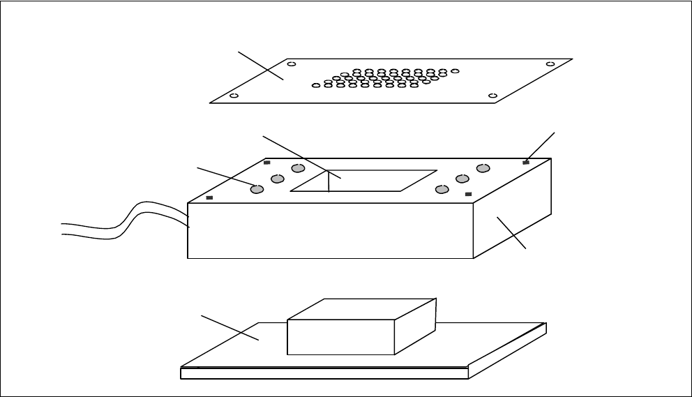
Product Overview
46
Revision 1.2, 2010-08-18
9.6.2.2 Alternative 2: Printing Solder
To print solder on the module a fixture must be used. The purpose of the fixture is to get a flat surface and fix the
stencil and module for printing. An example of how this fixture can be designed is shown in Figure 18.
S o ld e r p a ste sten cil
C a vity of th e m odu le T oo lin g pins
Va c u u m ho l e s
F ixture
Bo tto m
S
old
er
_
P
rint
ing
.
v
s
d
Figure 18 Solder Printing
1. Assemble the fixture to the bottom
2. Place the module in the cavity with the LGA pads upwards
3. Place the solder paste stencil on the fixture and make sure it fits to the tooling pins and the module
4. Apply vacuum to fix the solder paste stencil
5. Apply solder paste on the stencil and print by using a blade
6. Turn everything (bottom, fixture and stencil) upside down.
7. Separate carefully the bottom from the fixture
8. Pick the module by a nozzle and place in the right position on the board
9. Reflow the solder.
9.7 Inspection
Automatic inspection of the solder paste printing before assembly is highly recommended to ensure high yield and
good long term reliability.
9.8 Component Salvage
If it is intended to send a defect Unistone module back to the supplier for failure analysis, please note that during
the removal of this component no further defects must be introduced to the device, because this may hinder the
failure analysis at the supplier. This includes ESD precautions, not to apply high mechanical force for component
removal, and to prevent excess moisture content in the package during salvage (risk of pop corning failures).
Therefore if the maximum storage time out of the dry pack (see label on packing material) is exceeded after board
assembly, the PCB has to be dried 24h at 125°C before soldering off the defect component, because otherwise
too much moisture may have been accumulated.
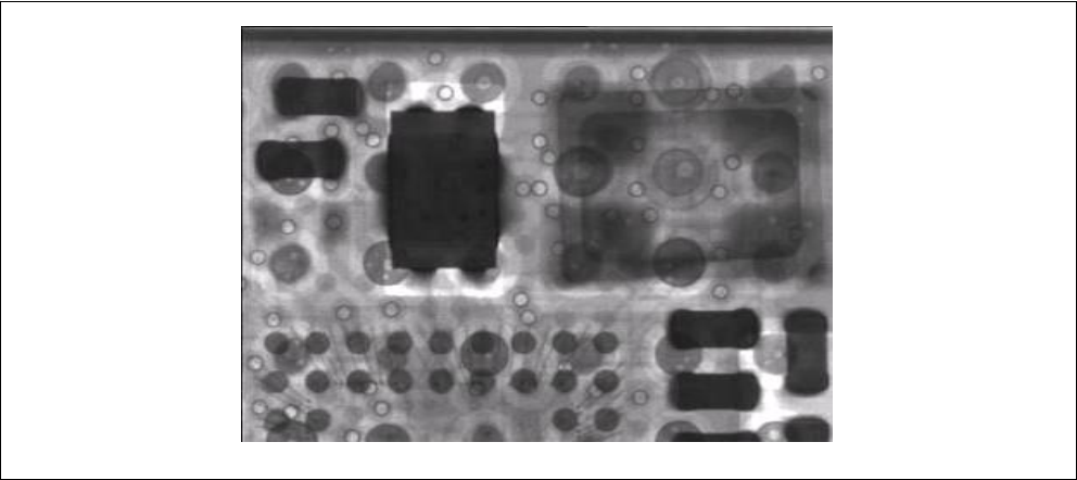
Product Overview
47
Revision 1.2, 2010-08-18
9.9 Voids in the Solder Joints
9.9.1 Expected Void Content and Reliability
The content of voids is larger on LGA modules than for modules with BGA or leads. At a LGA solder joint the
outgassing flux has a longer way to the surface of the solder and it has a relatively small surface to the air.
The void content of the UniStone module conforms to IPC-A-610D (25% or less voiding area/area).
Figure 19 shows an example of void-content at a module assembled at production site. Normally you can see the
whole spectra of void content variation within the same lot and occasion of assembly.
V
o
ids
_I
P
C
_A
_61
0 D
.v
s
d
Figure 19 X-ray Picture Showing Voids Conforming to IPC-A-610D
9.9.2 Parameters with an Impact on Voiding
If the void content has to be reduced following parameters have an impact.
Solderability on module and PCB
Bad solderability is often connected to oxidation and has therefore a major impact on voiding. Flux will get
entrapped on oxidized surfaces. In general, Ni/Au pads show fewer voids than HASL and OSP.
Solder paste
Higher activity of the flux will remove oxide rapidly and less flux will get entrapped.
Voiding increases with increasing solder paste exposure time, since long exposure time will result in more
oxidation and moisture pickup.
Pad size
A large soldering pad means that the outgassing flux has a longer way to the surface of the solder, and will thereby
create more voids.
Product Overview
48
Revision 1.2, 2010-08-18
Solder paste
Smaller powder size and higher metal load means more metal surface to deoxidize and thereby more entrapped
flux and voiding. Higher metal load does also mean higher viscosity and more difficult for outgassed flux to remove
from the solder.
Stencil thickness
A thick solder paste stencil means more surface area to the air and thereby easier for the outgassing flux to leave
the solder.
Temperature soldering profile
Too short preheat time means that the flux does not get enough time to react and flux get entrapped in the solder
and create voids.
Too long reflow time gives larger voids
Too short reflow time gives a fraction of voids

Product Overview
49
Revision 1.2, 2010-08-18
PAN1320-HCI-BT2.1
ENW89814A2MF
CONFIDENTIAL References
References
[1] Panasonics User’s Manual - Firmware Description (BMU_PBA31308_V2.01_UM_FD_Rev1.2.pdf)
This document is CONFIDENTIAL and can only distributed with NDA.
[2] Panasonic User’s Manual - Hardware Description (PAN1320_V12.01_UM_HD_Rev1.4.pdf)
This document is CONFIDENTIAL and can only distributed with NDA.
[3] Infineon Generic Quality Specification for Mobile Phones
(Generic Quality Specification for Mobile Phones V2.0_2007-08-16.pdf)

PAN1320-HCI-BT2.1
ENW89814A2MF
CONFIDENTIAL
Terminology
Product Overview
50
Revision 1.2, 2010-08-18
Terminology
A
ACK Acknowledgement
ACL Asynchronous Connection-oriented (logical transport)
AFH Adaptive Frequency Hopping
AHS Adaptive Hop Sequence
ARQ Automatic Repeat reQuest
B
b bit/bits (e.g. kb/s)
B Byte/Bytes (e.g. kB/s)
BALUN BALanced UNbalanced
BD_ADDR Bluetooth Device Address
BER Bit Error Rate
BMU BlueMoon Universal
BOM Bill Of Material
BT Bluetooth
BW Bandwidth
C
CDCT Clock Drift Compensation Task
CMOS Complementary Metal Oxide Semiconductor
COD Class Of Device
CODEC COder/DECoder
CPU Central Processing Unit
CQDDR Channel Quality Driven Data Rate
CRC Cyclic Redundancy Check
CTS Clear To Send (UART flow control signal)
CVSD Continuous Variable Slope Delta (modulation)
D
DC Direct Current
DDC Device Data Control
DH Data High-Rate (packet type)
DM Data Medium-Rate (packet type)
DMA Direct Memory Access
DPSK Differential Phase Shift Keying (modulation)
DQPSK Differential Quaternary Phase Shift Keying (modulation)
DSP Digital Signal Processor
DUT Device Under Test
E
EDR Enhanced Data Rate

PAN1320-HCI-BT2.1
ENW89814A2MF
CONFIDENTIAL
Terminology
Product Overview
51
Revision 1.2, 2010-08-18
EEPROM Electrically Erasable Programmable Read Only Memory
eSCO Extended Synchronous Connection-Oriented (logical transport)
EV Extended Voice (packet type)
F
FEC Forward Error Correction
FHS Frequency Hop Synchronization (packet)
FIFO First In First Out (buffer)
FM Frequency Modulation
FW Firmware
G
GFSK Gaussian Frequency Shift Keying (modulation)
GPIO General Purpose Input/Output
GSM Global System for Mobile communication
H
HCI Host Controller Interface
HCI+ Infineon Specific HCI command set
HEC Header Error Check
HV High quality Voice (packet type)
HW Hardware
I
I2C Inter-IC Control (bus)
I2S Inter-IC Sound (bus)
IAC Inquiry Access Code
ID IDentifier
IEEE Institute of Electrical and Electronics Engineers
IF Intermediate Frequency
ISM Industrial Scientific & Medical (frequency band)
J
JTAG Joint Test Action Group
L
LAN Local Area Network
LAP Lower Address Part
LM Link Manager
LMP Link Manager Protocol
LNA Low Noise Amplifier
LO Local Oscillator
LPM Low Power Mode(s) LPO
Low Power Oscillator
LSB Least Significant Bit/Byte
LT_ADDR Logical Transport Address

PAN1320-HCI-BT2.1
ENW89814A2MF
CONFIDENTIAL
Terminology
Product Overview
52
Revision 1.2, 2010-08-18
M
MSB Most Significant Bit/Byte
MSRS Master-Slave Role Switch
N
NC No Connection
NOP No OPeration
NVM Non-Volatile Memory
O
OCF Opcode Command Field
OGF Opcode Group Field
P
PA Power Amplifier
PCB Printed Circuit Board
PCM Pulse Coded Modulation
PDU Protocol Data Unit
PER Packet Error Rate
PIN Personal Identification Number
PLC Packet Loss Concealment
PLL Phase Locked Loop
PMU Power Management Unit
POR Power-On Reset
PTA Packet Traffic Arbitration
PTT Packet Type Table
Q
QoS Quality Of Service
R
RAM Random Access Memory
RF Radio Frequency
ROM Read Only Memory
RSSI Received Signal Strength Indication
RTS Request To Send (UART flow control signal)
RX Receive
RXD Receive Data (UART signal)
S
SCO Synchronous Connection-Oriented (logical transport)
SIG Special Interest Group (Bluetooth SIG)
SW Software
SYRI Synthesizer Reference Input
T
TBD To Be Determined

PAN1320-HCI-BT2.1
ENW89814A2MF
CONFIDENTIAL
Terminology
Product Overview
53
Revision 1.2, 2010-08-18
TCK Test Clock (JTAG
signal) TDI
Test Data In (JTAG signal)
TDO Test Data Out (JTAG signal)
TL Transport Layer
TMS Test Mode Select (JTAG signal)
TX Transmit
TXD Transmit Data (UART signal)
U
UART Universal Asynchronous Receiver & Transmitter
ULPM Ultra Low Power Mode
V
VCO Voltage Controlled Oscillator
W
WLAN Wireless LAN (Local Area Network)
