ATmega8A Datasheet Atmel 8159 8 Bit Avr Microcontroller
2017-12-16
: Pdf Atmel-8159-8-Bit-Avr-Microcontroller-Atmega8A Datasheet atmel-8159-8-bit-avr-microcontroller-atmega8a_datasheet 3750-178-5961 aftab
Open the PDF directly: View PDF ![]() .
.
Page Count: 394 [warning: Documents this large are best viewed by clicking the View PDF Link!]
- Introduction
- Features
- Table of Contents
- 1. Description
- 2. Configuration Summary
- 3. Ordering Information
- 4. Block Diagram
- 5. Pin Configurations
- 6. I/O Multiplexing
- 7. Resources
- 8. Data Retention
- 9. About Code Examples
- 10. Capacitive Touch Sensing
- 11. AVR CPU Core
- 12. AVR Memories
- 13. System Clock and Clock Options
- 14. Power Management and Sleep Modes
- 15. System Control and Reset
- 16. Interrupts
- 17. External Interrupts
- 18. I/O Ports
- 18.1. Overview
- 18.2. Ports as General Digital I/O
- 18.3. Alternate Port Functions
- 18.4. Register Description
- 18.4.1. SFIOR – Special Function IO Register
- 18.4.2. PORTB – The Port B Data Register
- 18.4.3. DDRB – The Port B Data Direction Register
- 18.4.4. PINB – The Port B Input Pins Address
- 18.4.5. PORTC – The Port C Data Register
- 18.4.6. DDRC – The Port C Data Direction Register
- 18.4.7. PINC – The Port C Input Pins Address
- 18.4.8. PORTD – The Port D Data Register
- 18.4.9. DDRD – The Port D Data Direction Register
- 18.4.10. PIND – The Port D Input Pins Address
- 19. 8-bit Timer/Counter0
- 20. Timer/Counter0 and Timer/Counter1 Prescalers
- 21. 16-bit Timer/Counter1
- 21.1. Features
- 21.2. Overview
- 21.3. Accessing 16-bit Registers
- 21.4. Timer/Counter Clock Sources
- 21.5. Counter Unit
- 21.6. Input Capture Unit
- 21.7. Output Compare Units
- 21.8. Compare Match Output Unit
- 21.9. Modes of Operation
- 21.10. Timer/Counter Timing Diagrams
- 21.11. Register Description
- 21.11.1. TCCR1A – Timer/Counter1 Control Register A
- 21.11.2. TCCR1B – Timer/Counter1 Control Register B
- 21.11.3. TCNT1L – Timer/Counter1 Low byte
- 21.11.4. TCNT1H – Timer/Counter1 High byte
- 21.11.5. OCR1AL – Output Compare Register 1 A Low byte
- 21.11.6. OCR1AH – Output Compare Register 1 A High byte
- 21.11.7. OCR1BL – Output Compare Register 1 B Low byte
- 21.11.8. OCR1BH – Output Compare Register 1 B High byte
- 21.11.9. ICR1L – Input Capture Register 1 Low byte
- 21.11.10. ICR1H – Input Capture Register 1 High byte
- 21.11.11. TIMSK – Timer/Counter Interrupt Mask Register
- 21.11.12. TIFR – Timer/Counter Interrupt Flag Register
- 22. 8-bit Timer/Counter2 with PWM and Asynchronous Operation
- 22.1. Features
- 22.2. Overview
- 22.3. Timer/Counter Clock Sources
- 22.4. Counter Unit
- 22.5. Output Compare Unit
- 22.6. Compare Match Output Unit
- 22.7. Modes of Operation
- 22.8. Timer/Counter Timing Diagrams
- 22.9. Asynchronous Operation of the Timer/Counter
- 22.10. Timer/Counter Prescaler
- 22.11. Register Description
- 22.11.1. TCCR2 – Timer/Counter Control Register
- 22.11.2. TCNT2 – Timer/Counter Register
- 22.11.3. OCR2 – Output Compare Register
- 22.11.4. ASSR – Asynchronous Status Register
- 22.11.5. TIMSK – Timer/Counter Interrupt Mask Register
- 22.11.6. TIFR – Timer/Counter Interrupt Flag Register
- 22.11.7. SFIOR – Special Function IO Register
- 23. SPI – Serial Peripheral Interface
- 24. USART - Universal Synchronous and Asynchronous serial Receiver and Transmitter
- 24.1. Features
- 24.2. Overview
- 24.3. Clock Generation
- 24.4. Frame Formats
- 24.5. USART Initialization
- 24.6. Data Transmission – The USART Transmitter
- 24.7. Data Reception – The USART Receiver
- 24.8. Asynchronous Data Reception
- 24.9. Multi-Processor Communication Mode
- 24.10. Accessing UBRRH/UCSRC Registers
- 24.11. Register Description
- 24.12. Examples of Baud Rate Setting
- 25. TWI - Two-wire Serial Interface
- 26. Analog Comparator
- 27. ADC - Analog to Digital Converter
- 28. Boot Loader Support – Read-While-Write Self-Programming
- 28.1. Features
- 28.2. Overview
- 28.3. Application and Boot Loader Flash Sections
- 28.4. Read-While-Write and No Read-While-Write Flash Sections
- 28.5. Boot Loader Lock Bits
- 28.6. Entering the Boot Loader Program
- 28.7. Addressing the Flash During Self-Programming
- 28.8. Self-Programming the Flash
- 28.8.1. Performing Page Erase by SPM
- 28.8.2. Filling the Temporary Buffer (Page Loading)
- 28.8.3. Performing a Page Write
- 28.8.4. Using the SPM Interrupt
- 28.8.5. Consideration While Updating Boot Loader Section (BLS)
- 28.8.6. Prevent Reading the RWW Section During Self-Programming
- 28.8.7. Setting the Boot Loader Lock Bits by SPM
- 28.8.8. EEPROM Write Prevents Writing to SPMCR
- 28.8.9. Reading the Fuse and Lock Bits from Software
- 28.8.10. Preventing Flash Corruption
- 28.8.11. Programming Time for Flash when Using SPM
- 28.8.12. Simple Assembly Code Example for a Boot Loader
- 28.8.13. ATmega8A Boot Loader Parameters
- 28.9. Register Description
- 29. Memory Programming
- 29.1. Program and Data Memory Lock Bits
- 29.2. Fuse Bits
- 29.3. Signature Bytes
- 29.4. Calibration Byte
- 29.5. Page Size
- 29.6. Parallel Programming Parameters, Pin Mapping, and Commands
- 29.7. Parallel Programming
- 29.7.1. Enter Programming Mode
- 29.7.2. Considerations for Efficient Programming
- 29.7.3. Chip Erase
- 29.7.4. Programming the Flash
- 29.7.5. Programming the EEPROM
- 29.7.6. Reading the Flash
- 29.7.7. Reading the EEPROM
- 29.7.8. Programming the Fuse Low Bits
- 29.7.9. Programming the Fuse High Bits
- 29.7.10. Programming the Lock Bits
- 29.7.11. Reading the Fuse and Lock Bits
- 29.7.12. Reading the Signature Bytes
- 29.7.13. Reading the Calibration Byte
- 29.7.14. Parallel Programming Characteristics
- 29.8. Serial Downloading
- 29.9. Serial Programming Pin Mapping
- 30. Electrical Characteristics – TA = -40°C to 85°C
- 31. Electrical Characteristics – TA = -40°C to 105°C
- 32. Typical Characteristics – TA = -40°C to 85°C
- 32.1. Active Supply Current
- 32.2. Idle Supply Current
- 32.3. Power-down Supply Current
- 32.4. Power-save Supply Current
- 32.5. Standby Supply Current
- 32.6. Pin Pull-up
- 32.7. Pin Driver Strength
- 32.8. Pin Thresholds and Hysteresis
- 32.9. Bod Thresholds and Analog Comparator Offset
- 32.10. Internal Oscillator Speed
- 32.11. Current Consumption of Peripheral Units
- 32.12. Current Consumption in Reset and Reset Pulsewidth
- 33. Typical Characteristics – TA = -40°C to 105°C
- 33.1. ATmega8A Typical Characteristics
- 33.1.1. Active Supply Current
- 33.1.2. Idle Supply Current
- 33.1.3. Power-down Supply Current
- 33.1.4. Power-save Supply Current
- 33.1.5. Standby Supply Current
- 33.1.6. Pin Pull-up
- 33.1.7. Pin Driver Strength
- 33.1.8. Pin Threshold and Hysteresis
- 33.1.9. BOD Threshold
- 33.1.10. Internal Oscillator Speed
- 33.1.11. Current Consumption of Peripheral Units
- 33.1.12. Current Consumption in Reset and Reset Pulsewidth
- 33.1. ATmega8A Typical Characteristics
- 34. Register Summary
- 35. Instruction Set Summary
- 36. Packaging Information
- 37. Errata
- 38. Datasheet Revision History

8-bit AVR Microcontroller
ATmega8A
DATASHEET COMPLETE
Introduction
The Atmel® ATmega8A is a low-power CMOS 8-bit microcontroller based on
the AVR® enhanced RISC architecture. By executing powerful instructions in
a single clock cycle, the ATmega8A achieves throughputs close to 1MIPS
per MHz. This empowers system designer to optimize the device for power
consumption versus processing speed.
Features
•High-performance, Low-power Atmel AVR 8-bit Microcontroller
•Advanced RISC Architecture
–130 Powerful Instructions - Most Single-clock Cycle Execution
–32 x 8 General Purpose Working Registers
–Fully Static Operation
–Up to 16MIPS Throughput at 16MHz
–On-chip 2-cycle Multiplier
•High Endurance Non-volatile Memory segments
–8KBytes of In-System Self-programmable Flash program
memory
–512Bytes EEPROM
–1KByte Internal SRAM
–Write/Erase Cycles: 10,000 Flash/100,000 EEPROM
–Data retention: 20 years at 85°C/100 years at 25°C(1)
–Optional Boot Code Section with Independent Lock Bits
• In-System Programming by On-chip Boot Program
• True Read-While-Write Operation
–Programming Lock for Software Security
•Atmel QTouch® library support
–Capacitive touch buttons, sliders and wheels
–Atmel QTouch and QMatrix acquisition
–Up to 64 sense channels
•Peripheral Features
–Two 8-bit Timer/Counters with Separate Prescaler, one Compare
Mode
Atmel-8159F-8-bit AVR Microcontroller_Datasheet_Complete-09/2015

–One 16-bit Timer/Counter with Separate Prescaler, Compare Mode, and Capture Mode
–Real Time Counter with Separate Oscillator
–Three PWM Channels
–8-channel ADC in TQFP and QFN/MLF package
• Eight Channels 10-bit Accuracy
–6-channel ADC in PDIP package
• Six Channels 10-bit Accuracy
–Byte-oriented Two-wire Serial Interface
–Programmable Serial USART
–Master/Slave SPI Serial Interface
–Programmable Watchdog Timer with Separate On-chip Oscillator
–On-chip Analog Comparator
•Special Microcontroller Features
–Power-on Reset and Programmable Brown-out Detection
–Internal Calibrated RC Oscillator
–External and Internal Interrupt Sources
–Five Sleep Modes: Idle, ADC Noise Reduction, Power-save, Power-down, and Standby
•I/O and Packages
–23 Programmable I/O Lines
–28-lead PDIP, 32-lead TQFP, and 32-pad QFN/MLF
•Operating Voltages
–2.7 - 5.5V
•Speed Grades
–0 - 16MHz
•Power Consumption at 4MHz, 3V, 25°C
–Active: 3.6mA
–Idle Mode: 1.0mA
–Power-down Mode: 0.5μA
Atmel ATmega8A [DATASHEET]
Atmel-8159F-8-bit AVR Microcontroller_Datasheet_Complete-09/2015
2

Table of Contents
Introduction......................................................................................................................1
Features.......................................................................................................................... 1
1. Description.................................................................................................................9
2. Configuration Summary...........................................................................................10
3. Ordering Information................................................................................................ 11
4. Block Diagram......................................................................................................... 12
5. Pin Configurations................................................................................................... 13
5.1. Pin Descriptions..........................................................................................................................15
5.2. Accessing 16-bit Registers.........................................................................................................17
6. I/O Multiplexing........................................................................................................20
7. Resources................................................................................................................21
8. Data Retention.........................................................................................................22
9. About Code Examples.............................................................................................23
10. Capacitive Touch Sensing....................................................................................... 24
11. AVR CPU Core........................................................................................................ 25
11.1. Overview.....................................................................................................................................25
11.2. ALU – Arithmetic Logic Unit........................................................................................................26
11.3. Status Register...........................................................................................................................26
11.4. General Purpose Register File................................................................................................... 28
11.5. Stack Pointer.............................................................................................................................. 29
11.6. Instruction Execution Timing...................................................................................................... 30
11.7. Reset and Interrupt Handling..................................................................................................... 31
12. AVR Memories.........................................................................................................33
12.1. Overview.....................................................................................................................................33
12.2. In-System Reprogrammable Flash Program Memory................................................................33
12.3. SRAM Data Memory...................................................................................................................34
12.4. EEPROM Data Memory............................................................................................................. 35
12.5. I/O Memory.................................................................................................................................36
12.6. Register Description................................................................................................................... 37
13. System Clock and Clock Options............................................................................ 44
13.1. Clock Systems and their Distribution..........................................................................................44
13.2. Clock Sources............................................................................................................................ 45
13.3. Crystal Oscillator........................................................................................................................ 46

13.4. Low-frequency Crystal Oscillator................................................................................................47
13.5. External RC Oscillator................................................................................................................ 48
13.6. Calibrated Internal RC Oscillator................................................................................................48
13.7. External Clock............................................................................................................................ 49
13.8. Timer/Counter Oscillator.............................................................................................................50
13.9. Register Description................................................................................................................... 50
14. Power Management and Sleep Modes................................................................... 52
14.1. Sleep Modes...............................................................................................................................52
14.2. Idle Mode....................................................................................................................................53
14.3. ADC Noise Reduction Mode.......................................................................................................53
14.4. Power-down Mode......................................................................................................................53
14.5. Power-save Mode.......................................................................................................................53
14.6. Standby Mode............................................................................................................................ 54
14.7. Minimizing Power Consumption................................................................................................. 54
14.8. Register Description................................................................................................................... 55
15. System Control and Reset.......................................................................................57
15.1. Resetting the AVR...................................................................................................................... 57
15.2. Reset Sources............................................................................................................................57
15.3. Internal Voltage Reference.........................................................................................................60
15.4. Watchdog Timer......................................................................................................................... 61
15.5. Timed Sequences for Changing the Configuration of the Watchdog Timer............................... 61
15.6. Register Description................................................................................................................... 62
16. Interrupts................................................................................................................. 66
16.1. Interrupt Vectors in ATmega8A...................................................................................................66
16.2. Register Description................................................................................................................... 70
17. External Interrupts................................................................................................... 73
17.1. Register Description................................................................................................................... 73
18. I/O Ports.................................................................................................................. 77
18.1. Overview.....................................................................................................................................77
18.2. Ports as General Digital I/O........................................................................................................78
18.3. Alternate Port Functions.............................................................................................................81
18.4. Register Description................................................................................................................... 90
19. 8-bit Timer/Counter0..............................................................................................101
19.1. Features................................................................................................................................... 101
19.2. Overview...................................................................................................................................101
19.3. Timer/Counter Clock Sources.................................................................................................. 102
19.4. Counter Unit............................................................................................................................. 102
19.5. Operation..................................................................................................................................103
19.6. Timer/Counter Timing Diagrams...............................................................................................103
19.7. Register Description................................................................................................................. 103
20. Timer/Counter0 and Timer/Counter1 Prescalers...................................................108
20.1. Overview...................................................................................................................................108
Atmel ATmega8A [DATASHEET]
Atmel-8159F-8-bit AVR Microcontroller_Datasheet_Complete-09/2015
4

20.2. Internal Clock Source............................................................................................................... 108
20.3. Prescaler Reset........................................................................................................................108
20.4. External Clock Source..............................................................................................................108
20.5. Register Description................................................................................................................. 109
21. 16-bit Timer/Counter1............................................................................................ 111
21.1. Features....................................................................................................................................111
21.2. Overview...................................................................................................................................111
21.3. Accessing 16-bit Registers....................................................................................................... 113
21.4. Timer/Counter Clock Sources...................................................................................................116
21.5. Counter Unit..............................................................................................................................116
21.6. Input Capture Unit.....................................................................................................................117
21.7. Output Compare Units..............................................................................................................119
21.8. Compare Match Output Unit.....................................................................................................121
21.9. Modes of Operation..................................................................................................................122
21.10. Timer/Counter Timing Diagrams.............................................................................................. 130
21.11. Register Description................................................................................................................. 131
22. 8-bit Timer/Counter2 with PWM and Asynchronous Operation............................. 147
22.1. Features................................................................................................................................... 147
22.2. Overview...................................................................................................................................147
22.3. Timer/Counter Clock Sources.................................................................................................. 148
22.4. Counter Unit............................................................................................................................. 148
22.5. Output Compare Unit................................................................................................................149
22.6. Compare Match Output Unit.....................................................................................................151
22.7. Modes of Operation..................................................................................................................152
22.8. Timer/Counter Timing Diagrams...............................................................................................156
22.9. Asynchronous Operation of the Timer/Counter........................................................................ 158
22.10. Timer/Counter Prescaler.......................................................................................................... 159
22.11. Register Description................................................................................................................. 160
23. SPI – Serial Peripheral Interface........................................................................... 170
23.1. Features................................................................................................................................... 170
23.2. Overview...................................................................................................................................170
23.3. SS Pin Functionality................................................................................................................. 173
23.4. Data Modes.............................................................................................................................. 174
23.5. Register Description................................................................................................................. 175
24. USART - Universal Synchronous and Asynchronous serial Receiver and
Transmitter.............................................................................................................180
24.1. Features................................................................................................................................... 180
24.2. Overview...................................................................................................................................180
24.3. Clock Generation......................................................................................................................182
24.4. Frame Formats.........................................................................................................................185
24.5. USART Initialization..................................................................................................................186
24.6. Data Transmission – The USART Transmitter......................................................................... 187
24.7. Data Reception – The USART Receiver.................................................................................. 190
24.8. Asynchronous Data Reception.................................................................................................193
24.9. Multi-Processor Communication Mode.....................................................................................196
Atmel ATmega8A [DATASHEET]
Atmel-8159F-8-bit AVR Microcontroller_Datasheet_Complete-09/2015
5

24.10. Accessing UBRRH/UCSRC Registers..................................................................................... 197
24.11. Register Description................................................................................................................. 198
24.12. Examples of Baud Rate Setting............................................................................................... 207
25. TWI - Two-wire Serial Interface..............................................................................211
25.1. Features....................................................................................................................................211
25.2. Overview...................................................................................................................................211
25.3. Two-Wire Serial Interface Bus Definition..................................................................................213
25.4. Data Transfer and Frame Format.............................................................................................214
25.5. Multi-master Bus Systems, Arbitration and Synchronization....................................................217
25.6. Using the TWI...........................................................................................................................218
25.7. Multi-master Systems and Arbitration.......................................................................................235
25.8. Register Description................................................................................................................. 236
26. Analog Comparator............................................................................................... 243
26.1. Overview...................................................................................................................................243
26.2. Analog Comparator Multiplexed Input...................................................................................... 243
26.3. Register Description................................................................................................................. 244
27. ADC - Analog to Digital Converter.........................................................................248
27.1. Features................................................................................................................................... 248
27.2. Overview...................................................................................................................................248
27.3. Starting a Conversion...............................................................................................................250
27.4. Prescaling and Conversion Timing...........................................................................................250
27.5. Changing Channel or Reference Selection.............................................................................. 252
27.6. ADC Noise Canceler................................................................................................................ 253
27.7. ADC Conversion Result............................................................................................................257
27.8. Register Description................................................................................................................. 257
28. Boot Loader Support – Read-While-Write Self-Programming............................... 266
28.1. Features................................................................................................................................... 266
28.2. Overview...................................................................................................................................266
28.3. Application and Boot Loader Flash Sections............................................................................266
28.4. Read-While-Write and No Read-While-Write Flash Sections...................................................267
28.5. Boot Loader Lock Bits.............................................................................................................. 269
28.6. Entering the Boot Loader Program...........................................................................................270
28.7. Addressing the Flash During Self-Programming...................................................................... 271
28.8. Self-Programming the Flash.....................................................................................................272
28.9. Register Description................................................................................................................. 280
29. Memory Programming...........................................................................................283
29.1. Program and Data Memory Lock Bits.......................................................................................283
29.2. Fuse Bits...................................................................................................................................284
29.3. Signature Bytes........................................................................................................................ 286
29.4. Calibration Byte........................................................................................................................ 286
29.5. Page Size................................................................................................................................. 286
29.6. Parallel Programming Parameters, Pin Mapping, and Commands..........................................286
29.7. Parallel Programming...............................................................................................................288
29.8. Serial Downloading...................................................................................................................297
Atmel ATmega8A [DATASHEET]
Atmel-8159F-8-bit AVR Microcontroller_Datasheet_Complete-09/2015
6

29.9. Serial Programming Pin Mapping.............................................................................................297
30. Electrical Characteristics – TA = -40°C to 85°C.....................................................302
30.1. DC Characteristics....................................................................................................................302
30.2. Speed Grades.......................................................................................................................... 304
30.3. Clock Characteristics................................................................................................................304
30.4. System and Reset Characteristics........................................................................................... 305
30.5. Two-wire Serial Interface Characteristics................................................................................. 306
30.6. SPI Timing Characteristics....................................................................................................... 308
30.7. ADC Characteristics................................................................................................................. 309
31. Electrical Characteristics – TA = -40°C to 105°C...................................................312
31.1. DC Characteristics....................................................................................................................312
32. Typical Characteristics – TA = -40°C to 85°C........................................................314
32.1. Active Supply Current...............................................................................................................314
32.2. Idle Supply Current...................................................................................................................318
32.3. Power-down Supply Current.....................................................................................................321
32.4. Power-save Supply Current......................................................................................................322
32.5. Standby Supply Current........................................................................................................... 323
32.6. Pin Pull-up................................................................................................................................ 326
32.7. Pin Driver Strength................................................................................................................... 328
32.8. Pin Thresholds and Hysteresis.................................................................................................332
32.9. Bod Thresholds and Analog Comparator Offset.......................................................................337
32.10. Internal Oscillator Speed..........................................................................................................339
32.11. Current Consumption of Peripheral Units.................................................................................346
32.12. Current Consumption in Reset and Reset Pulsewidth............................................................. 349
33. Typical Characteristics – TA = -40°C to 105°C......................................................351
33.1. ATmega8A Typical Characteristics...........................................................................................351
34. Register Summary.................................................................................................380
35. Instruction Set Summary....................................................................................... 382
36. Packaging Information...........................................................................................387
36.1. 32A........................................................................................................................................... 387
36.2. 28P3......................................................................................................................................... 388
36.3. 32M1-A.....................................................................................................................................389
37. Errata.....................................................................................................................390
37.1. ATmega8A, rev. L.....................................................................................................................390
38. Datasheet Revision History................................................................................... 392
38.1. Rev.8159F – 07/2015............................................................................................................... 392
38.2. Rev.8159E – 02/2013...............................................................................................................392
38.3. Rev.8159D – 02/11...................................................................................................................392
38.4. DRH_Rev.8159C – 07/09.........................................................................................................392
38.5. Rev.8159B – 05/09...................................................................................................................392
Atmel ATmega8A [DATASHEET]
Atmel-8159F-8-bit AVR Microcontroller_Datasheet_Complete-09/2015
7


1. Description
The Atmel AVR core combines a rich instruction set with 32 general purpose working registers. All the 32
registers are directly connected to the Arithmetic Logic Unit (ALU), allowing two independent registers to
be accessed in one single instruction executed in one clock cycle. The resulting architecture is more code
efficient while achieving throughputs up to ten times faster than conventional CISC microcontrollers.
The ATmega8A provides the following features: 8K bytes of In-System Programmable Flash with Read-
While- Write capabilities, 512 bytes of EEPROM, 1K byte of SRAM, 23 general purpose I/O lines, 32
general purpose working registers, three flexible Timer/Counters with compare modes, internal and
external interrupts, a serial programmable USART, one byte oriented Two-wire Serial Interface, a 6-
channel ADC (eight channels in TQFP and QFN/MLF packages) with 10-bit accuracy, a programmable
Watchdog Timer with Internal Oscillator, an SPI serial port, and five software selectable power saving
modes. The Idle mode stops the CPU while allowing the SRAM, Timer/Counters, one SPI port, and
interrupt system to continue functioning. The Power-down mode saves the register contents but freezes
the Oscillator, disabling all other chip functions until the next Interrupt or Hardware Reset. In Power-save
mode, the asynchronous timer continues to run, allowing the user to maintain a timer base while the rest
of the device is sleeping. The ADC Noise Reduction mode stops the CPU and all I/O modules except
asynchronous timer and ADC, to minimize switching noise during ADC conversions. In Standby mode,
the crystal/resonator Oscillator is running while the rest of the device is sleeping. This allows very fast
start-up combined with low-power consumption.
Atmel offers the QTouch library for embedding capacitive touch buttons, sliders and wheels functionality
into AVR microcontrollers. The patented charge-transfer signal acquisition offers robust sensing and
includes fully debounced reporting of touch keys and includes Adjacent Key Suppression® (AKS®)
technology for unambiguous detection of key events. The easy-to-use QTouch Composer allows you to
explore, develop and debug your own touch applications.
The device is manufactured using Atmel’s high density non-volatile memory technology. The On-chip ISP
Flash allows the program memory to be reprogrammed In-System through an SPI serial interface, by a
conventional nonvolatile memory programmer, or by an On-chip Boot program running on the AVR core.
The Boot program can use any interface to download the application program in the Application Flash
memory. Software in the Boot Flash section will continue to run while the Application Flash section is
updated, providing true Read-While-Write operation. By combining an 8-bit RISC CPU with In-System
Self-Programmable Flash on a monolithic chip, the Atmel ATmega8A is a powerful microcontroller that
provides a highly flexible and cost effective solution to many embedded control applications.
The device is supported with a full suite of program and system development tools including: C
Compilers, Macro Assemblers, Program Debugger/Simulators, In-Circuit Emulators, and Evaluation kit.
Atmel ATmega8A [DATASHEET]
Atmel-8159F-8-bit AVR Microcontroller_Datasheet_Complete-09/2015
9

2. Configuration Summary
Features ATmega8A
Pin count 32
Flash (KB) 8
SRAM (KB) 1
EEPROM (Bytes) 512
General Purpose I/O pins 23
SPI 1
TWI (I2C) 1
USART 1
ADC 10-bit 15ksps
ADC channels 6 (8 in TQFP and QFN/MLF packages)
AC propagation delay Typ 400ns
8-bit Timer/Counters 2
16-bit Timer/Counters 1
PWM channels 3
RC Oscillator +/-3%
Operating voltage 2.7 - 5.5V
Max operating frequency 16MHz
Temperature range -40°C to +105°C
Atmel ATmega8A [DATASHEET]
Atmel-8159F-8-bit AVR Microcontroller_Datasheet_Complete-09/2015
10

3. Ordering Information
Speed (MHz) Power Supply Ordering Code(2) Package(1) Operational Range
16 2.7 - 5.5V
ATmega8A-AU
ATmega8A-AUR(3)
ATmega8A-PU
ATmega8A-MU
ATmega8A-MUR(3)
32A
32A
28P3
32M1-A
32M1-A
Industrial (-40oC to 85oC)
ATmega8A-AN
ATmega8A-ANR(3)
ATmega8A-MN
ATmega8A-MNR(3)
ATmega8A-PN
32A
32A
32M1-A
32M1-A
28P3
Extended (-40oC to 105oC)
Note:
1. This device can also be supplied in wafer form. Please contact your local Atmel sales office for
detailed ordering information and minimum quantities.
2. Pb-free packaging, complies to the European Directive for Restriction of Hazardous Substances
(RoHS directive). Also Halide free and fully Green.
3. Tape and Reel
Package Type
32A 32-lead, Thin (1.0mm) Plastic Quad Flat Package (TQFP)
28P3 28-lead, 0.300” Wide, Plastic Dual Inline Package (PDIP)
32M1-A 32-pad, 5 x 5 x 1.0mm body, lead pitch 0.50mm, Quad Flat No-Lead/Micro Lead Frame
Package (QFN/MLF)
Atmel ATmega8A [DATASHEET]
Atmel-8159F-8-bit AVR Microcontroller_Datasheet_Complete-09/2015
11
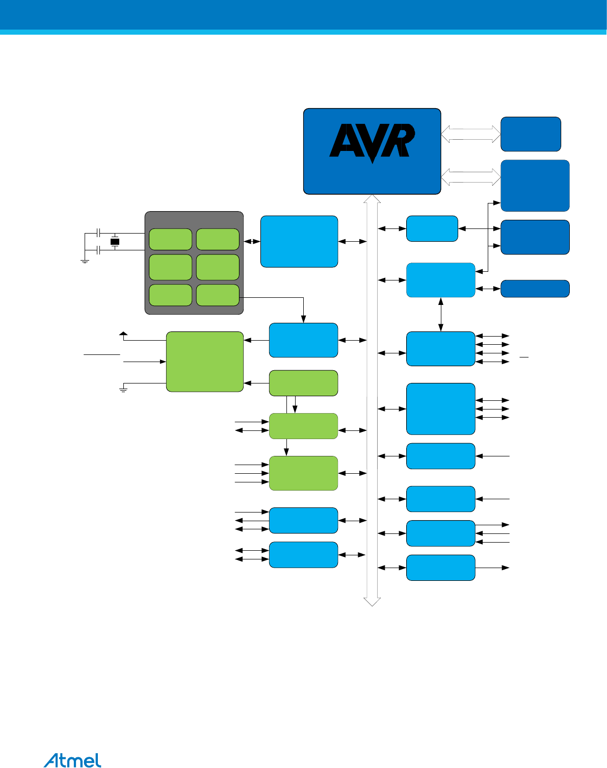
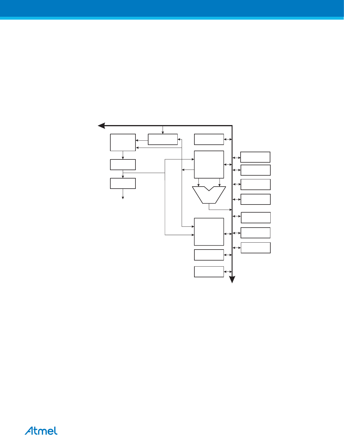
4. Block Diagram
Figure 4-1 Block Diagram
CPU
USART
ADC
ADC[7:0]
AREF
RxD
TxD
XCK
I/O
PORTS
SRAM
EXTINT
FLASH
NVM
programming
TC 0
(8-bit)
SPI
AC
AIN0
AIN1
ADCMUX
EEPROM
EEPROMIF
TC 1
(16-bit)
OC1A/B
T1
ICP1
TC 2
(8-bit async)
TWI
SDA
SCL
Internal
Reference
Watchdog
Timer
Power
management
and clock
control
VCC
GND
Power
Supervision
POR/BOD &
RESET
XTAL2/
TOSC2
RESET
XTAL1/
TOSC1
INT[1:0]
T0
MISO
MOSI
SCK
SS
OC2
PB[7:0]
PC[6:0]
PD[7:0]
Clock generation
1/2/4/8MHz
Calib RC
1MHz int
osc
32.768kHz
XOSC
External
clock
8 MHz
Crystal Osc
D
A
T
A
B
U
S
12MHz
External
RC Osc
PARPROG
Serial
Programming
Atmel ATmega8A [DATASHEET]
Atmel-8159F-8-bit AVR Microcontroller_Datasheet_Complete-09/2015
12
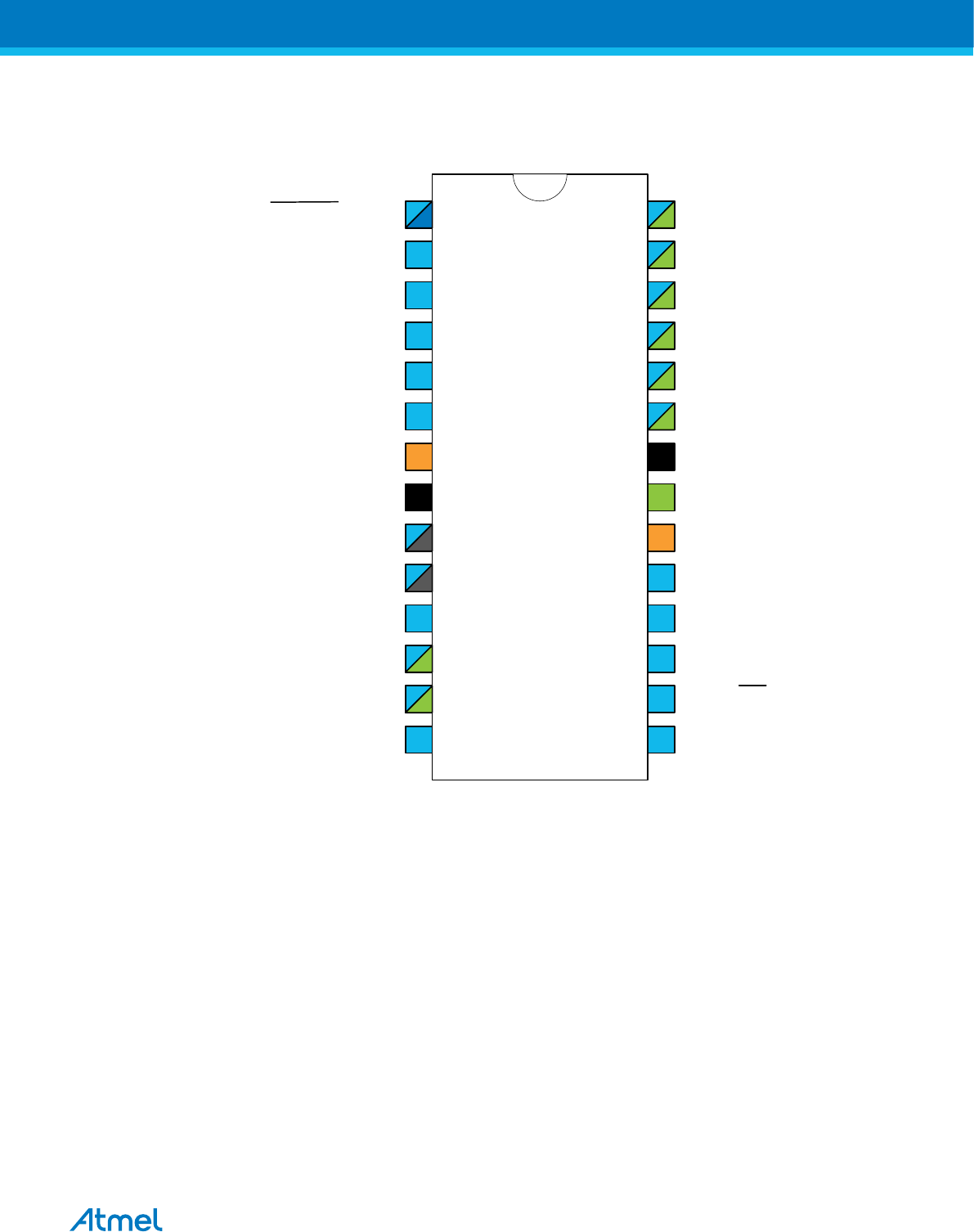
5. Pin Configurations
Figure 5-1 PDIP
1
2
3
4
5
6
7
8
9
13
10
11
12
14
GND
15
20
19
18
17
16
GND
24
23
22
21
28
27
26
25
AREF
AVCC
VCC
(RESET) PC6
(RXD) PD0
(TXD) PD1
(INT0) PD2
(INT1) PD3
(XCK/T0) PD4
(XTAL1/TOSC1) PB6
(XTAL2/TOSC2) PB7
(T1) PD5
(AIN0) PD6
(AIN1) PD7
(ICP1) PB0 PB1 (OC1A)
PB2 (SS/OC1B)
PB3 (MOSI/OC2)
PB4 (MISO)
PB5 (SCK)
PC0 (ADC0)
PC1 (ADC1)
PC2 (ADC2)
PC3 (ADC3)
PC4 (ADC4/SDA)
PC5 (ADC5/SCL)
Atmel ATmega8A [DATASHEET]
Atmel-8159F-8-bit AVR Microcontroller_Datasheet_Complete-09/2015
13
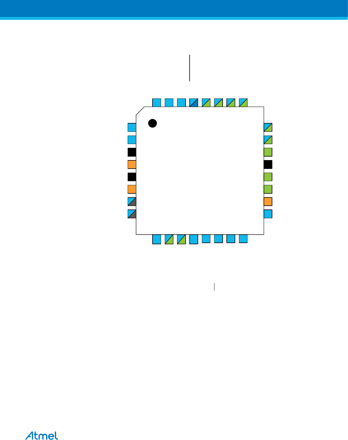
Figure 5-2 TQFP Top View
1
2
3
4
32
31
30
29
28
27
26
5
6
7
8
24
23
22
21
20
19
18
17
25
9
10
11
12
13
14
15
16
PD0 (RXD)
PD1 (TXD)
PD2 (INT0)
PC6 (RESET)
PC2 (ADC2)
PC3 (ADC3)
PC4 (ADC4/SDA)
PC5 (ADC5/SCL)
PC0 (ADC0)
PC1 (ADC1)
GND
ADC6
AVCC
PB5 (SCK)
AREF
ADC7
(INT1) PD3
(XCK/T0) PD4
GND
VCC
GND
VCC
(XTAL1/TOSC1) PB6
(XTAL2/TOSC2) PB7
(T1) PD5
(AIN0) PD6
(AIN1) PD7
(ICP1) PB0
(OC1A) PB1
(SS/OC1B) PB2
(MOSI/OC2) PB3
(MISO) PB4
Atmel ATmega8A [DATASHEET]
Atmel-8159F-8-bit AVR Microcontroller_Datasheet_Complete-09/2015
14
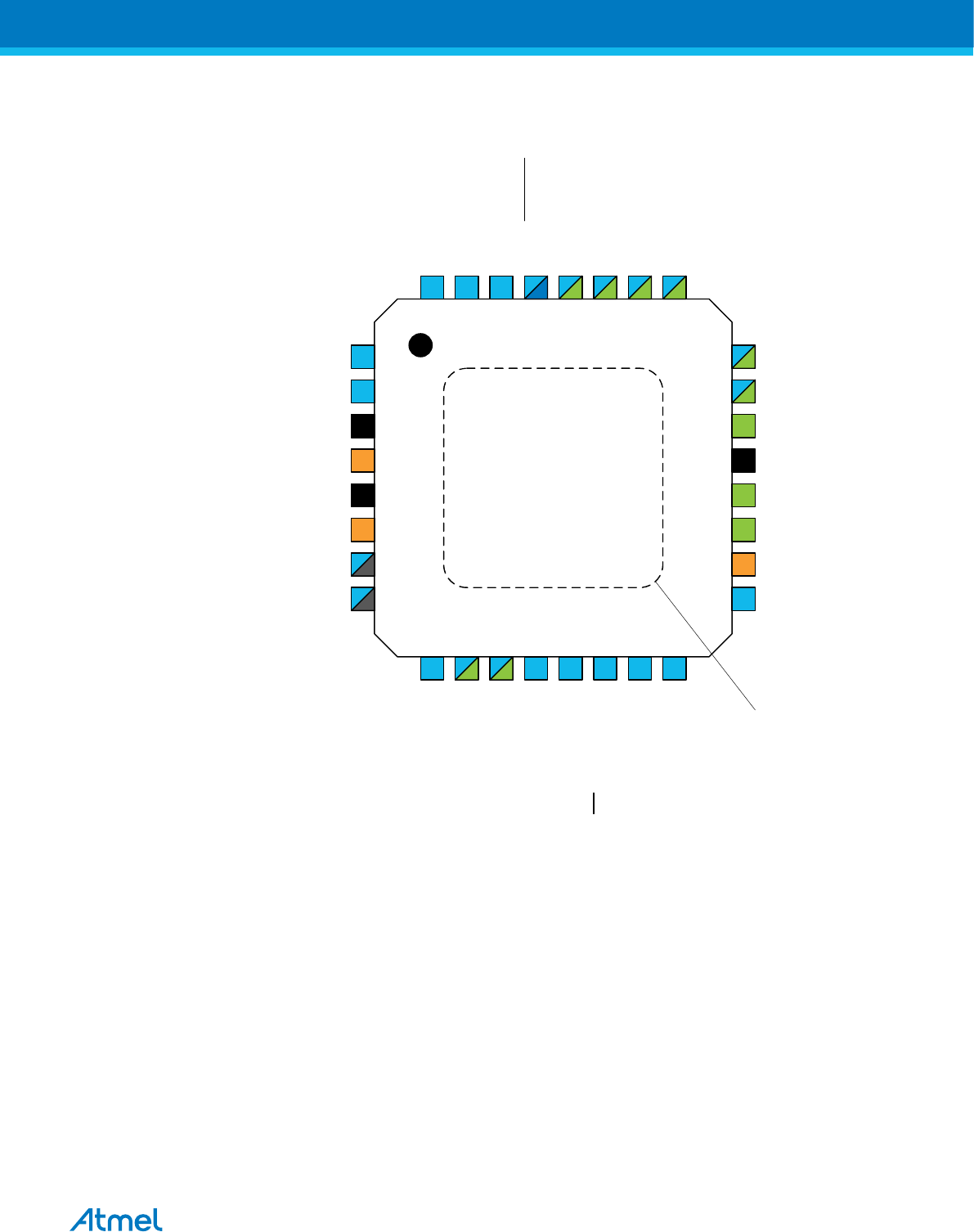
Figure 5-3 MLF Top View
1
2
3
4
32
31
30
29
28
27
26
5
6
7
8
24
23
22
21
20
19
18
17
25
9
10
11
12
13
14
15
16
PD0 (RXD)
PD1 (TXD)
PD2 (INT0)
PC6 (RESET)
PC2 (ADC2)
PC3 (ADC3)
PC4 (ADC4/SDA)
PC5 (ADC5/SCL)
PC0 (ADC0)
PC1 (ADC1)
GND
ADC6
AVCC
PB5 (SCK)
AREF
ADC7
(INT1) PD3
(XCK/T0) PD4
GND
VCC
GND
VCC
(XTAL1/TOSC1) PB6
(XTAL2/TOSC2) PB7
(T1) PD5
(AIN0) PD6
(AIN1) PD7
(ICP1) PB0
(OC1A) PB1
(SS/OC1B) PB2
(MOSI/OC2) PB3
(MISO) PB4
NOTE:
The large center pad underneath
the MLF packages is made of
metal and internally connected to
GND. It should be soldered or
glued to the PCB to ensure good
mechanical stability. If the center
pad is left unconneted, the
package might loosen from the
PCB.
5.1. Pin Descriptions
5.1.1. VCC
Digital supply voltage.
5.1.2. GND
Ground.
5.1.3. Port B (PB7:PB0) – XTAL1/XTAL2/TOSC1/TOSC2
Port B is an 8-bit bi-directional I/O port with internal pull-up resistors (selected for each bit). The Port B
output buffers have symmetrical drive characteristics with both high sink and source capability. As inputs,
Port B pins that are externally pulled low will source current if the pull-up resistors are activated. The Port
B pins are tri-stated when a reset condition becomes active, even if the clock is not running.
Atmel ATmega8A [DATASHEET]
Atmel-8159F-8-bit AVR Microcontroller_Datasheet_Complete-09/2015
15

Depending on the clock selection fuse settings, PB6 can be used as input to the inverting Oscillator
amplifier and input to the internal clock operating circuit.
Depending on the clock selection fuse settings, PB7 can be used as output from the inverting Oscillator
amplifier.
If the Internal Calibrated RC Oscillator is used as chip clock source, PB7:6 is used as TOSC2:1 input for
the Asynchronous Timer/Counter2 if the AS2 bit in ASSR is set.
The various special features of Port B are elaborated in Alternate Functions of Port B and System Clock
and Clock Options.
5.1.4. Port C (PC5:PC0)
Port C is an 7-bit bi-directional I/O port with internal pull-up resistors (selected for each bit). The Port C
output buffers have symmetrical drive characteristics with both high sink and source capability. As inputs,
Port C pins that are externally pulled low will source current if the pull-up resistors are activated. The Port
C pins are tri-stated when a reset condition becomes active, even if the clock is not running.
5.1.5. PC6/RESET
If the RSTDISBL Fuse is programmed, PC6 is used as an I/O pin. Note that the electrical characteristics
of PC6 differ from those of the other pins of Port C.
If the RSTDISBL Fuse is unprogrammed, PC6 is used as a Reset input. A low level on this pin for longer
than the minimum pulse length will generate a Reset, even if the clock is not running. The minimum pulse
length is given in Table 30-5. Shorter pulses are not guaranteed to generate a Reset.
The various special features of Port C are elaborated in Alternate Functions of Port C.
5.1.6. Port D (PD7:PD0)
Port D is an 8-bit bi-directional I/O port with internal pull-up resistors (selected for each bit). The Port D
output buffers have symmetrical drive characteristics with both high sink and source capability. As inputs,
Port D pins that are externally pulled low will source current if the pull-up resistors are activated. The Port
D pins are tri-stated when a reset condition becomes active, even if the clock is not running.
Port D also serves the functions of various special features of the ATmega8A as listed in Alternate
Functions of Port D.
5.1.7. RESET
Reset input. A low level on this pin for longer than the minimum pulse length will generate a reset, even if
the clock is not running. The minimum pulse length is given in Table 30-5. Shorter pulses are not
guaranteed to generate a reset.
5.1.8. AVCC
AVCC is the supply voltage pin for the A/D Converter, Port C (3:0), and ADC (7:6). It should be externally
connected to VCC, even if the ADC is not used. If the ADC is used, it should be connected to VCC through
a low-pass filter. Note that Port C (5:4) use digital supply voltage, VCC.
5.1.9. AREF
AREF is the analog reference pin for the A/D Converter.
5.1.10. ADC7:6 (TQFP and QFN/MLF Package Only)
In the TQFP and QFN/MLF package, ADC7:6 serve as analog inputs to the A/D converter. These pins are
powered from the analog supply and serve as 10-bit ADC channels.
Atmel ATmega8A [DATASHEET]
Atmel-8159F-8-bit AVR Microcontroller_Datasheet_Complete-09/2015
16

5.2. Accessing 16-bit Registers
The TCNT1, OCR1A/B, and ICR1 are 16-bit registers that can be accessed by the AVR CPU via the 8-bit
data bus. A 16-bit register must be byte accessed using two read or write operations. The 16-bit timer has
a single 8-bit register for temporary storing of the High byte of the 16-bit access. The same temporary
register is shared between all 16-bit registers within the 16-bit timer. Accessing the Low byte triggers the
16-bit read or write operation. When the Low byte of a 16-bit register is written by the CPU, the High byte
stored in the temporary register, and the Low byte written are both copied into the 16-bit register in the
same clock cycle. When the Low byte of a 16-bit register is read by the CPU, the High byte of the 16-bit
register is copied into the temporary register in the same clock cycle as the Low byte is read.
Not all 16-bit accesses uses the temporary register for the High byte. Reading the OCR1A/B 16-bit
registers does not involve using the temporary register.
To do a 16-bit write, the High byte must be written before the Low byte. For a 16-bit read, the Low byte
must be read before the High byte.
The following code examples show how to access the 16-bit Timer Registers assuming that no interrupts
updates the temporary register. The same principle can be used directly for accessing the OCR1A/B and
ICR1 Registers. Note that when using “C”, the compiler handles the 16-bit access.
Assembly Code Example(1)
:.
; Set TCNT1 to 0x01FF
ldi r17,0x01
ldi r16,0xFF
out TCNT1H,r17
out TCNT1L,r16
; Read TCNT1 into r17:r16
in r16,TCNT1L
in r17,TCNT1H
:.
C Code Example(1)
unsigned int i;
:.
/* Set TCNT1 to 0x01FF */
TCNT1 = 0x1FF;
/* Read TCNT1 into i */
i = TCNT1;
:.
Note: 1. See About Code Examples.
The assembly code example returns the TCNT1 value in the r17:r16 Register pair.
It is important to notice that accessing 16-bit registers are atomic operations. If an interrupt occurs
between the two instructions accessing the 16-bit register, and the interrupt code updates the temporary
register by accessing the same or any other of the 16-bit Timer Registers, then the result of the access
outside the interrupt will be corrupted. Therefore, when both the main code and the interrupt code update
the temporary register, the main code must disable the interrupts during the 16-bit access.
The following code examples show how to do an atomic read of the TCNT1 Register contents. Reading
any of the OCR1A/B or ICR1 Registers can be done by using the same principle.
Atmel ATmega8A [DATASHEET]
Atmel-8159F-8-bit AVR Microcontroller_Datasheet_Complete-09/2015
17

Asesmbly Code Example(1)
TIM16_ReadTCNT1:
; Save global interrupt flag
in r18,SREG
; Disable interrupts
cli
; Read TCNT1 into r17:r16
in r16,TCNT1L
in r17,TCNT1H
; Restore global interrupt flag
out SREG,r18
ret
C Code Example(1)
unsigned int TIM16_ReadTCNT1( void )
{
unsigned char sreg;
unsigned int i;
/* Save global interrupt flag */
sreg = SREG;
/* Disable interrupts */
_CLI();
/* Read TCNT1 into i */
i = TCNT1;
/* Restore global interrupt flag */
SREG = sreg;
return i;
}
Note: 1. See About Code Examples.
The assembly code example returns the TCNT1 value in the r17:r16 Register pair.
The following code examples show how to do an atomic write of the TCNT1 Register contents. Writing
any of the OCR1A/B or ICR1 Registers can be done by using the same principle.
Assembly Code Example(1)
TIM16_WriteTCNT1:
; Save global interrupt flag
in r18,SREG
; Disable interrupts
cli
; Set TCNT1 to r17:r16
out TCNT1H,r17
out TCNT1L,r16
; Restore global interrupt flag
out SREG,r18
ret
C Code Example(1)
void TIM16_WriteTCNT1( unsigned int i )
{
unsigned char sreg;
unsigned int i;
/* Save global interrupt flag */
Atmel ATmega8A [DATASHEET]
Atmel-8159F-8-bit AVR Microcontroller_Datasheet_Complete-09/2015
18

sreg = SREG;
/* Disable interrupts */
_CLI();
/* Set TCNT1 to i */
TCNT1 = i;
/* Restore global interrupt flag */
SREG = sreg;
}
Note: 1. See About Code Examples.
The assembly code example requires that the r17:r16 Register pair contains the value to be written to
TCNT1.
Related Links
About Code Examples on page 23
Atmel ATmega8A [DATASHEET]
Atmel-8159F-8-bit AVR Microcontroller_Datasheet_Complete-09/2015
19

6. I/O Multiplexing
Each pin is by default controlled by the PORT as a general purpose I/O and alternatively it can be
assigned to one of the peripheral functions. This table describes the peripheral signals multiplexed to the
PORT I/O pins.
Table 6-1 PORT Function Multiplexing
PAD Pin # EXTINT PCINT AC Custom OSC TC1(16-
bit)
TC2(8-bit) USART SPI Misc
PD[4] 14 PCINT20 ACO - - O1CA - -
PB[6] 1 PCINT06 - - EXTCLK - - - -
PD[5] 2 PCINT21 AINP1 - - CLK1 - - SII
PD[6] 3 PCINT22 AINP0 - - ICP1 - - - SDO
PD[7] 4 PCINT23 AINN0 - - - TC2-OCB - - SDI
PB[2] 5 PCINT02 - CLO0 CLKOUT TC1-OCB - - SS
PB[3] 6 PCINT03 - - - TC2-OCA TXD MOSI
PB[4] 7 PCINT04 - - - - - RXD MISO
PB[5] 8 PCINT05 - CLO1 - - - XCK SCK
PC[4] 9 PCINT12 AINN1 - - - - - -
PC[5] 10 INT0 PCINT13 AINN2 - - - - - -
PC[6]/
RESET
13 PCINT14 - - - - - - HVRST/d
W
VCC 11
GND 12
Atmel ATmega8A [DATASHEET]
Atmel-8159F-8-bit AVR Microcontroller_Datasheet_Complete-09/2015
20


8. Data Retention
Reliability Qualification results show that the projected data retention failure rate is much less than 1 PPM
over 20 years at 85°C or 100 years at 25°C.
Atmel ATmega8A [DATASHEET]
Atmel-8159F-8-bit AVR Microcontroller_Datasheet_Complete-09/2015
22

9. About Code Examples
This datasheet contains simple code examples that briefly show how to use various parts of the device.
These code examples assume that the part specific header file is included before compilation. Be aware
that not all C compiler vendors include bit definitions in the header files and interrupt handling in C is
compiler dependent. Please confirm with the C compiler documentation for more details.
For I/O registers located in extended I/O map, “IN”, “OUT”, “SBIS”, “SBIC”, “CBI”, and “SBI” instructions
must be replaced with instructions that allow access to extended I/O. Typically “LDS” and “STS”
combined with “SBRS”, “SBRC”, “SBR”, and “CBR”.
Atmel ATmega8A [DATASHEET]
Atmel-8159F-8-bit AVR Microcontroller_Datasheet_Complete-09/2015
23

10. Capacitive Touch Sensing
The Atmel QTouch Library provides a simple to use solution to realize touch sensitive interfaces on most
Atmel AVR microcontrollers. The QTouch Library includes support for the QTouch and QMatrix®
acquisition methods.
Touch sensing can be added to any application by linking the appropriate Atmel QTouch Library for the
AVR Microcontroller. This is done by using a simple set of APIs to define the touch channels and sensors,
and then calling the touch sensing API’s to retrieve the channel information and determine the touch
sensor states.
The QTouch Library is FREE and downloadable from the Atmel website at the following location:
www.atmel.com/qtouchlibrary. For implementation details and other information, refer to the Atmel
QTouch Library User Guide - also available for download from the Atmel website.
Atmel ATmega8A [DATASHEET]
Atmel-8159F-8-bit AVR Microcontroller_Datasheet_Complete-09/2015
24
11. AVR CPU Core
11.1. Overview
This section discusses the Atmel AVR core architecture in general. The main function of the CPU core is
to ensure correct program execution. The CPU must therefore be able to access memories, perform
calculations, control peripherals, and handle interrupts.
Figure 11-1 Block Diagram of the AVR MCU Architecture
Flash
Program
Memory
Instruction
Register
Instruction
Decoder
Program
Counter
Control Line s
32 x 8
General
Purpose
Registrers
ALU
Status
and Control
I/O Line s
EEPROM
Data Bus 8-bit
Data
SRAM
Direct Addre s s ing
Indire ct Addre s s ing
Interrupt
Unit
SPI
Unit
Watchdog
Timer
Analog
Comparator
i/O Module 2
i/O Module1
i/O Module n
In order to maximize performance and parallelism, the AVR uses a Harvard architecture – with separate
memories and buses for program and data. Instructions in the Program memory are executed with a
single level pipelining. While one instruction is being executed, the next instruction is pre-fetched from the
Program memory. This concept enables instructions to be executed in every clock cycle. The Program
memory is In-System Reprogrammable Flash memory.
The fast-access Register File contains 32 x 8-bit general purpose working registers with a single clock
cycle access time. This allows single-cycle Arithmetic Logic Unit (ALU) operation. In a typical ALU
operation, two operands are output from the Register File, the operation is executed, and the result is
stored back in the Register File – in one clock cycle.
Six of the 32 registers can be used as three 16-bit indirect address register pointers for Data Space
addressing – enabling efficient address calculations. One of the these address pointers can also be used
as an address pointer for look up tables in Flash Program memory. These added function registers are
the 16-bit X-, Y-, and Z-register, described later in this section.
The ALU supports arithmetic and logic operations between registers or between a constant and a
register. Single register operations can also be executed in the ALU. After an arithmetic operation, the
Status Register is updated to reflect information about the result of the operation.
Atmel ATmega8A [DATASHEET]
Atmel-8159F-8-bit AVR Microcontroller_Datasheet_Complete-09/2015
25

The Program flow is provided by conditional and unconditional jump and call instructions, able to directly
address the whole address space. Most AVR instructions have a single 16-bit word format. Every
Program memory address contains a 16- or 32-bit instruction.
Program Flash memory space is divided in two sections, the Boot program section and the Application
program section. Both sections have dedicated Lock Bits for write and read/write protection. The SPM
instruction that writes into the Application Flash memory section must reside in the Boot program section.
During interrupts and subroutine calls, the return address Program Counter (PC) is stored on the Stack.
The Stack is effectively allocated in the general data SRAM, and consequently the Stack size is only
limited by the total SRAM size and the usage of the SRAM. All user programs must initialize the SP in the
reset routine (before subroutines or interrupts are executed). The Stack Pointer SP is read/write
accessible in the I/O space. The data SRAM can easily be accessed through the five different addressing
modes supported in the AVR architecture.
The memory spaces in the AVR architecture are all linear and regular memory maps.
A flexible interrupt module has its control registers in the I/O space with an additional global interrupt
enable bit in the Status Register. All interrupts have a separate Interrupt Vector in the Interrupt Vector
table. The interrupts have priority in accordance with their Interrupt Vector position. The lower the
Interrupt Vector address, the higher the priority.
The I/O memory space contains 64 addresses for CPU peripheral functions as Control Registers, SPI,
and other I/O functions. The I/O Memory can be accessed directly, or as the Data Space locations
following those of the Register File, 0x20 - 0x5F. In addition, the ATmega8A has Extended I/O space from
$60 in SRAM where only the ST/STS/STD and LD/LDS/LDD instructions can be used.
11.2. ALU – Arithmetic Logic Unit
The high-performance Atmel AVR ALU operates in direct connection with all the 32 general purpose
working registers. Within a single clock cycle, arithmetic operations between general purpose registers or
between a register and an immediate are executed. The ALU operations are divided into three main
categories – arithmetic, logical, and bit-functions. Some implementations of the architecture also provide
a powerful multiplier supporting both signed/unsigned multiplication and fractional format. See the
“Instruction Set” section for a detailed description.
11.3. Status Register
The Status Register contains information about the result of the most recently executed arithmetic
instruction. This information can be used for altering program flow in order to perform conditional
operations. Note that the Status Register is updated after all ALU operations, as specified in the
Instruction Set Reference. This will in many cases remove the need for using the dedicated compare
instructions, resulting in faster and more compact code.
The Status Register is not automatically stored when entering an interrupt routine and restored when
returning from an interrupt. This must be handled by software.
Atmel ATmega8A [DATASHEET]
Atmel-8159F-8-bit AVR Microcontroller_Datasheet_Complete-09/2015
26

11.3.1. SREG – The AVR Status Register
When using the I/O specific commands IN and OUT, the I/O addresses 0x00 - 0x3F must be used. When
addressing I/O Registers as data space using LD and ST instructions, 0x20 must be added to these offset
addresses. The device is a complex microcontroller with more peripheral units than can be supported
within the 64 location reserved in Opcode for the IN and OUT instructions. For the Extended I/O space
from 0x60 in SRAM, only the ST/STS/STD and LD/LDS/LDD instructions can be used.
Name: SREG
Offset: 0x3F
Reset: 0x00
Property:
When addressing I/O Registers as data space the offset address is 0x5F
Bit 7 6 5 4 3 2 1 0
I T H S V N Z C
Access R/W R/W R/W R/W R/W R/W R/W R/W
Reset 0 0 0 0 0 0 0 0
Bit 7 – I: Global Interrupt Enable
The Global Interrupt Enable bit must be set for the interrupts to be enabled. The individual interrupt
enable control is then performed in separate control registers. If the Global Interrupt Enable Register is
cleared, none of the interrupts are enabled independent of the individual interrupt enable settings. The I-
bit is cleared by hardware after an interrupt has occurred, and is set by the RETI instruction to enable
subsequent interrupts. The I-bit can also be set and cleared by the application with the SEI and CLI
instructions, as described in the Instruction Set Reference.
Bit 6 – T: Bit Copy Storage
The Bit Copy instructions BLD (Bit LoaD) and BST (Bit STore) use the T-bit as source or destination for
the operated bit. A bit from a register in the Register File can be copied into T by the BST instruction, and
a bit in T can be copied into a bit in a register in the Register File by the BLD instruction.
Bit 5 – H: Half Carry Flag
The Half Carry Flag H indicates a Half Carry in some arithmetic operations. Half Carry is useful in BCD
arithmetic. See the “Instruction Set Description” for detailed information.
Bit 4 – S: Sign Bit, S = N ⊕ V
The S-bit is always an exclusive or between the Negative Flag N and the Two’s Complement Overflow
Flag V. See the “Instruction Set Description” for detailed information.
Bit 3 – V: Two’s Complement Overflow Flag
The Two’s Complement Overflow Flag V supports two’s complement arithmetics. See the “Instruction Set
Description” for detailed information.
Bit 2 – N: Negative Flag
The Negative Flag N indicates a negative result in an arithmetic or logic operation. See the “Instruction
Set Description” for detailed information.
Bit 1 – Z: Zero Flag
The Zero Flag Z indicates a zero result in an arithmetic or logic operation. See the “Instruction Set
Description” for detailed information.
Atmel ATmega8A [DATASHEET]
Atmel-8159F-8-bit AVR Microcontroller_Datasheet_Complete-09/2015
27
Bit 0 – C: Carry Flag
The Carry Flag C indicates a Carry in an arithmetic or logic operation. See the “Instruction Set
Description” for detailed information.
11.4. General Purpose Register File
The Register File is optimized for the Atmel AVR Enhanced RISC instruction set. In order to achieve the
required performance and flexibility, the following input/output schemes are supported by the Register
File:
•One 8-bit output operand and one 8-bit result input.
•Two 8-bit output operands and one 8-bit result input.
•Two 8-bit output operands and one 16-bit result input.
•One 16-bit output operand and one 16-bit result input.
The following figure shows the structure of the 32 general purpose working registers in the CPU.
Figure 11-2 AVR CPU General Purpose Working Registers
7
0
Addr.
R0
0x00
R1
0x01
R2
0x02
…
R13
0x0D
Genera l
R14
0x0E
Purpose
R15
0x0F
Working
R16
0x10
Registers
R17
0x11
…
R26
0x1A
X-re giste r Low Byte
R27
0x1B
X-re giste r High Byte
R28
0x1C
Y-re giste r Low Byte
R29
0x1D
Y-re giste r High Byte
R30
0x1E
Z-regis te r Low Byte
R31
0x1F
Z-regis te r High Byte
Most of the instructions operating on the Register File have direct access to all registers, and most of
them are single cycle instructions.
As shown in the figure above, each register is also assigned a Data memory address, mapping them
directly into the first 32 locations of the user Data Space. Although not being physically implemented as
SRAM locations, this memory organization provides great flexibility in access of the registers, as the X-,
Y-, and Z-pointer Registers can be set to index any register in the file.
11.4.1. The X-register, Y-register and Z-register
The registers R26:R31 have some added functions to their general purpose usage. These registers are
16-bit address pointers for indirect addressing of the Data Space. The three indirect address registers X,
Y and Z are defined as described in the following figure.
Atmel ATmega8A [DATASHEET]
Atmel-8159F-8-bit AVR Microcontroller_Datasheet_Complete-09/2015
28
Figure 11-3 The X-, Y- and Z-Registers
15
XH
XL
0
X-re gis te r
7
0
7
0
R27 (0x1B)
R26 (0x1A)
15
YH
YL
0
Y-re gis te r
7
0
7
0
R29 (0x1D)
R28 (0x1C)
15
ZH
ZL
0
Z-re gis te r
7
0
7
0
R31 (0x1F)
R30 (0x1E)
In the different addressing modes these address registers have functions as fixed displacement,
automatic increment, and automatic decrement (see the Instruction Set Reference for details).
11.5. Stack Pointer
The Stack is mainly used for storing temporary data, for storing local variables and for storing return
addresses after interrupts and subroutine calls. Note that the Stack is implemented as growing from
higher to lower memory locations. The Stack Pointer Register always points to the top of the Stack. The
Stack Pointer points to the data SRAM Stack area where the Subroutine and Interrupt Stacks are located.
A Stack PUSH command will decrease the Stack Pointer.
The Stack in the data SRAM must be defined by the program before any subroutine calls are executed or
interrupts are enabled. Initial Stack Pointer value equals the last address of the internal SRAM and the
Stack Pointer must be set to point above start of the SRAM, see Figure Data Memory Map in SRAM Data
Memory.
See table below for Stack Pointer details.
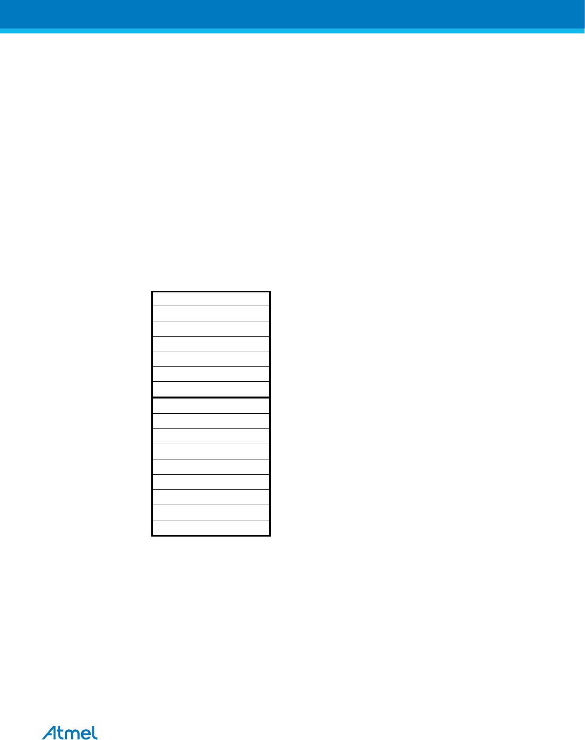
Table 11-1 Stack Pointer instructions
Instruction Stack pointer Description
PUSH Decremented by 1 Data is pushed onto the stack
CALL
ICALL
RCALL
Decremented by 2 Return address is pushed onto the stack with a subroutine call or
interrupt
POP Incremented by 1 Data is popped from the stack
RET
RETI
Incremented by 2 Return address is popped from the stack with return from subroutine or
return from interrupt
The Atmel AVR Stack Pointer is implemented as two 8-bit registers in the I/O space. The number of bits
actually used is implementation dependent. Note that the data space in some implementations of the AVR
architecture is so small that only SPL is needed. In this case, the SPH Register will not be present.
Related Links
SRAM Data Memory on page 34
Atmel ATmega8A [DATASHEET]
Atmel-8159F-8-bit AVR Microcontroller_Datasheet_Complete-09/2015
29
11.5.1. SPH and SPL - Stack Pointer High and Stack Pointer Low Register
Bit
15
14
13
12
11
10
9
8
0x3E
S P15
S P14
S P13
S P12
S P11
S P10
S P9
S P8
S PH
0x3D
S P7
S P6
S P5
S P4
S P3
S P2
S P1
S P0
S PL
7
6
5
4
3
2
1
0
Read/Write
R/W
R/W
R/W
R/W
R/W
R/W
R/W
R/W
R/W
R/W
R/W
R/W
R/W
R/W
R/W
R/W
Initial Value
0
0
0
0
0
0
0
0
0
0
0
0
0
0
0
0
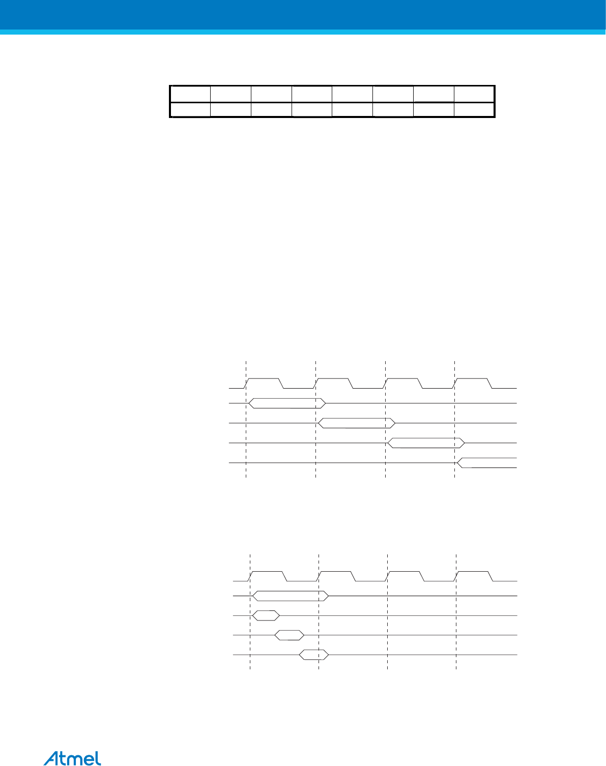
11.6. Instruction Execution Timing
This section describes the general access timing concepts for instruction execution. The Atmel AVR CPU
is driven by the CPU clock clkCPU, directly generated from the selected clock source for the chip. No
internal clock division is used.
The following figure shows the parallel instruction fetches and instruction executions enabled by the
Harvard architecture and the fast-access Register File concept. This is the basic pipelining concept to
obtain up to 1 MIPS per MHz with the corresponding unique results for functions per cost, functions per
clocks, and functions per power-unit.
Figure 11-4 The Parallel Instruction Fetches and Instruction Executions
clk
1s t Instruction Fe tch
1s t Instruction Execute
2nd Ins truction Fe tch
2nd Ins truction Execute
3rd Ins truction Fetch
3rd Ins truction Execute
4th Ins truction Fetch
T1 T2 T3 T4
CPU
The next figure shows the internal timing concept for the Register File. In a single clock cycle an ALU
operation using two register operands is executed, and the result is stored back to the destination
register.
Figure 11-5 Single Cycle ALU Operation
Total Exe cution Time
Re gis te r Operands Fetch
ALU Opera tion Execute
Re sult Write Back
T1 T2 T3 T4
clkCP U
Atmel ATmega8A [DATASHEET]
Atmel-8159F-8-bit AVR Microcontroller_Datasheet_Complete-09/2015
30

11.7. Reset and Interrupt Handling
The Atmel AVR provides several different interrupt sources. These interrupts and the separate Reset
Vector each have a separate Program Vector in the Program memory space. All interrupts are assigned
individual enable bits which must be written logic one together with the Global Interrupt Enable bit in the
Status Register in order to enable the interrupt. Depending on the Program Counter value, interrupts may
be automatically disabled when Boot Lock Bits BLB02 or BLB12 are programmed. This feature improves
software security. See the section Memory Programming for details.
The lowest addresses in the Program memory space are by default defined as the Reset and Interrupt
Vectors. The complete list of Vectors is shown in Interrupts . The list also determines the priority levels of
the different interrupts. The lower the address the higher is the priority level. RESET has the highest
priority, and next is INT0 – the External Interrupt Request 0. The Interrupt Vectors can be moved to the
start of the boot Flash section by setting the Interrupt Vector Select (IVSEL) bit in the General Interrupt
Control Register (GICR). Refer to Interrupts for more information. The Reset Vector can also be moved to
the start of the boot Flash section by programming the BOOTRST Fuse, see Boot Loader Support –
Read-While-Write Self-Programming.
When an interrupt occurs, the Global Interrupt Enable I-bit is cleared and all interrupts are disabled. The
user software can write logic one to the I-bit to enable nested interrupts. All enabled interrupts can then
interrupt the current interrupt routine. The I-bit is automatically set when a Return from Interrupt
instruction – RETI – is executed.
There are basically two types of interrupts. The first type is triggered by an event that sets the Interrupt
Flag. For these interrupts, the Program Counter is vectored to the actual Interrupt Vector in order to
execute the interrupt handling routine, and hardware clears the corresponding Interrupt Flag. Interrupt
Flags can also be cleared by writing a logic one to the flag bit position(s) to be cleared. If an interrupt
condition occurs while the corresponding interrupt enable bit is cleared, the Interrupt Flag will be set and
remembered until the interrupt is enabled, or the flag is cleared by software. Similarly, if one or more
interrupt conditions occur while the global interrupt enable bit is cleared, the corresponding Interrupt
Flag(s) will be set and remembered until the global interrupt enable bit is set, and will then be executed by
order of priority.
The second type of interrupts will trigger as long as the interrupt condition is present. These interrupts do
not necessarily have Interrupt Flags. If the interrupt condition disappears before the interrupt is enabled,
the interrupt will not be triggered.
When the AVR exits from an interrupt, it will always return to the main program and execute one more
instruction before any pending interrupt is served.
Note that the Status Register is not automatically stored when entering an interrupt routine, nor restored
when returning from an interrupt routine. This must be handled by software.
When using the CLI instruction to disable interrupts, the interrupts will be immediately disabled. No
interrupt will be executed after the CLI instruction, even if it occurs simultaneously with the CLI instruction.
The following example shows how this can be used to avoid interrupts during the timed EEPROM write
sequence.
Atmel ATmega8A [DATASHEET]
Atmel-8159F-8-bit AVR Microcontroller_Datasheet_Complete-09/2015
31

Assembly Code Example
in r16, SREG ; store SREG value
cli ; disable interrupts during timed sequence
sbi EECR, EEMWE ; start EEPROM write
sbi EECR, EEWE
out SREG, r16 ; restore SREG value (I-bit)
C Code Example
char cSREG;
cSREG = SREG; /* store SREG value */
/* disable interrupts during timed sequence */
_CLI();
EECR |= (1<<EEMWE); /* start EEPROM write */
EECR |= (1<<EEWE);
SREG = cSREG; /* restore SREG value (I-bit) */
When using the SEI instruction to enable interrupts, the instruction following SEI will be executed before
any pending interrupts, as shown in the following example.
Assembly Code Example
sei ; set global interrupt enable
sleep ; enter sleep, waiting for interrupt
; note: will enter sleep before any pending
; interrupt(s)
C Code Example
_enable_interrupt(); /* set global interrupt enable */
_SLEEP(); /* enter sleep, waiting for interrupt */
/* note: will enter sleep before any pending interrupt(s) */
Related Links
Memory Programming on page 283
Interrupts on page 66
Boot Loader Support – Read-While-Write Self-Programming on page 266
11.7.1. Interrupt Response Time
The interrupt execution response for all the enabled Atmel AVR interrupts is four clock cycles minimum.
After four clock cycles, the Program Vector address for the actual interrupt handling routine is executed.
During this 4-clock cycle period, the Program Counter is pushed onto the Stack. The Vector is normally a
jump to the interrupt routine, and this jump takes three clock cycles. If an interrupt occurs during
execution of a multi-cycle instruction, this instruction is completed before the interrupt is served. If an
interrupt occurs when the MCU is in sleep mode, the interrupt execution response time is increased by
four clock cycles. This increase comes in addition to the start-up time from the selected sleep mode.
A return from an interrupt handling routine takes four clock cycles. During these four clock cycles, the
Program Counter (2 bytes) is popped back from the Stack, the Stack Pointer is incremented by 2, and the
I-bit in SREG is set.
Atmel ATmega8A [DATASHEET]
Atmel-8159F-8-bit AVR Microcontroller_Datasheet_Complete-09/2015
32

12. AVR Memories
12.1. Overview
This section describes the different memories in the Atmel AVR ATmega8A. The AVR architecture has
two main memory spaces, the Data memory and the Program Memory space. In addition, the ATmega8A
features an EEPROM Memory for data storage. All three memory spaces are linear and regular.
12.2. In-System Reprogrammable Flash Program Memory
The ATmega8A contains 8K bytes On-chip In-System Reprogrammable Flash memory for program
storage. Since all AVR instructions are 16- or 32-bits wide, the Flash is organized as 4K x 16 bits. For
software security, the Flash Program memory space is divided into two sections, Boot Program section
and Application Program section.
The Flash memory has an endurance of at least 10,000 write/erase cycles. The ATmega8A Program
Counter (PC) is 12 bits wide, thus addressing the 4K Program memory locations. The operation of Boot
Program section and associated Boot Lock Bits for software protection are described in detail in Boot
Loader Support – Read-While-Write Self-Programming. Memory Programming contains a detailed
description on Flash Programming in SPI- or Parallel Programming mode.
Constant tables can be allocated within the entire Program memory address space (see the LPM – Load
Program memory instruction description).
Timing diagrams for instruction fetch and execution are presented in Instruction Execution Timing.
Figure 12-1 Program Memory Map
$000
$FFF
Applica tion Fla s h Se ction
Boot Fla sh S e ction
Atmel ATmega8A [DATASHEET]
Atmel-8159F-8-bit AVR Microcontroller_Datasheet_Complete-09/2015
33
Related Links
Boot Loader Support – Read-While-Write Self-Programming on page 266
Memory Programming on page 283
Instruction Execution Timing on page 30
12.3. SRAM Data Memory
The figure below shows how the Atmel AVR ATmega8A SRAM Memory is organized.
The lower 1120 Data memory locations address the Register File, the I/O Memory, and the internal data
SRAM. The first 96 locations address the Register File and I/O Memory, and the next 1024 locations
address the internal data SRAM.
The five different addressing modes for the Data memory cover: Direct, Indirect with Displacement,
Indirect, Indirect with Pre-decrement, and Indirect with Post-increment. In the Register File, registers R26
to R31 feature the indirect addressing pointer registers.
The direct addressing reaches the entire data space.
The Indirect with Displacement mode reaches 63 address locations from the base address given by the
Y- or Z-register.
When using register indirect addressing modes with automatic pre-decrement and post-increment, the
address registers X, Y and Z are decremented or incremented.
The 32 general purpose working registers, 64 I/O Registers, and the 1024 bytes of internal data SRAM in
the ATmega8A are all accessible through all these addressing modes. The Register File is described in
General Purpose Register File.
Figure 12-2 Data Memory Map
Re gis te r File
R0
R1
R2
R29
R30
R31
I/O Re gis te rs
$00
$01
$02
...
$3D
$3E
$3F
...
$0000
$0001
$0002
$001D
$001E
$001F
$0020
$0021
$0022
...
$005D
$005E
$005F
...
Data Addres s Space
$0060
$0061
$045E
$045F
...
Interna l SRAM
Atmel ATmega8A [DATASHEET]
Atmel-8159F-8-bit AVR Microcontroller_Datasheet_Complete-09/2015
34
Related Links
General Purpose Register File on page 28
12.3.1. Data Memory Access Times
This section describes the general access timing concepts for internal memory access. The internal data
SRAM access is performed in two clkCPU cycles as described in the figure below.
Figure 12-3 On-chip Data SRAM Access Cycles
clk
WR
RD
Data
Data
Addre s s Addre ss Va lid
T1 T2 T3
Compute Addre s s
Re a d Write
CPU
Memory Vccess Instruction Next Ins truction
12.4. EEPROM Data Memory
The Atmel AVR ATmega8A contains 512 bytes of data EEPROM memory. It is organized as a separate
data space, in which single bytes can be read and written. The EEPROM has an endurance of at least
100,000 write/erase cycles. The access between the EEPROM and the CPU is described bellow,
specifying the EEPROM Address Registers, the EEPROM Data Register, and the EEPROM Control
Register.
Memory Programming contains a detailed description on EEPROM Programming in SPI- or Parallel
Programming mode.
Related Links
Memory Programming on page 283
12.4.1. EEPROM Read/Write Access
The EEPROM Access Registers are accessible in the I/O space.
The write access time for the EEPROM is given in Table 12-1 EEPROM Programming Time on page
42. A self-timing function, however, lets the user software detect when the next byte can be written. If
the user code contains instructions that write the EEPROM, some precautions must be taken. In heavily
filtered power supplies, VCC is likely to rise or fall slowly on Power-up/down. This causes the device for
some period of time to run at a voltage lower than specified as minimum for the clock frequency used.
See Preventing EEPROM Corruption on page 36 for details on how to avoid problems in these
situations.
In order to prevent unintentional EEPROM writes, a specific write procedure must be followed. Refer to
the description of the EEPROM Control Register for details on this.
Atmel ATmega8A [DATASHEET]
Atmel-8159F-8-bit AVR Microcontroller_Datasheet_Complete-09/2015
35

When the EEPROM is read, the CPU is halted for four clock cycles before the next instruction is
executed. When the EEPROM is written, the CPU is halted for two clock cycles before the next instruction
is executed.
12.4.2. EEPROM Write during Power-down Sleep Mode
When entering Power-down sleep mode while an EEPROM write operation is active, the EEPROM write
operation will continue, and will complete before the Write Access time has passed. However, when the
write operation is completed, the Oscillator continues running, and as a consequence, the device does
not enter Power-down entirely. It is therefore recommended to verify that the EEPROM write operation is
completed before entering Power-down.
12.4.3. Preventing EEPROM Corruption
During periods of low VCC, the EEPROM data can be corrupted because the supply voltage is too low for
the CPU and the EEPROM to operate properly. These issues are the same as for board level systems
using EEPROM, and the same design solutions should be applied.
An EEPROM data corruption can be caused by two situations when the voltage is too low. First, a regular
write sequence to the EEPROM requires a minimum voltage to operate correctly. Second, the CPU itself
can execute instructions incorrectly, if the supply voltage is too low.
EEPROM data corruption can easily be avoided by following this design recommendation:
Keep the AVR RESET active (low) during periods of insufficient power supply voltage. This can be done
by enabling the internal Brown-out Detector (BOD). If the detection level of the internal BOD does not
match the needed detection level, an external low VCC Reset Protection circuit can be used. If a reset
occurs while a write operation is in progress, the write operation will be completed provided that the
power supply voltage is sufficient.
12.5. I/O Memory
The I/O space definition of the ATmega8A is shown in Register Summary.
All ATmega8A I/Os and peripherals are placed in the I/O space. The I/O locations are accessed by the IN
and OUT instructions, transferring data between the 32 general purpose working registers and the I/O
space. I/O Registers within the address range 0x00 - 0x1F are directly bit-accessible using the SBI and
CBI instructions. In these registers, the value of single bits can be checked by using the SBIS and SBIC
instructions. Refer to the instruction set section for more details. When using the I/O specific commands
IN and OUT, the I/O addresses 0x00 - 0x3F must be used. When addressing I/O Registers as data space
using LD and ST instructions, 0x20 must be added to these addresses. The ATmega8A is a complex
microcontroller with more peripheral units than can be supported within the 64 location reserved in
Opcode for the IN and OUT instructions. For the Extended I/O space from 0x60 - 0xFF in SRAM, only the
ST/STS/STD and LD/LDS/LDD instructions can be used. The Extended I/O space is replaced with SRAM
locations when the ATmega8A is in the ATmega103 compatibility mode.
For compatibility with future devices, reserved bits should be written to zero if accessed. Reserved I/O
memory addresses should never be written.
Some of the Status Flags are cleared by writing a logical one to them. Note that the CBI and SBI
instructions will operate on all bits in the I/O Register, writing a one back into any flag read as set, thus
clearing the flag. The CBI and SBI instructions work with registers 0x00 to 0x1F only.
The I/O and Peripherals Control Registers are explained in later sections.
Related Links
Register Summary on page 380
Atmel ATmega8A [DATASHEET]
Atmel-8159F-8-bit AVR Microcontroller_Datasheet_Complete-09/2015
36

12.6. Register Description
Atmel ATmega8A [DATASHEET]
Atmel-8159F-8-bit AVR Microcontroller_Datasheet_Complete-09/2015
37

12.6.1. EEARL – The EEPROM Address Register Low
When using the I/O specific commands IN and OUT, the I/O addresses 0x00 - 0x3F must be used. When
addressing I/O Registers as data space using LD and ST instructions, 0x20 must be added to these offset
addresses. The device is a complex microcontroller with more peripheral units than can be supported
within the 64 location reserved in Opcode for the IN and OUT instructions. For the Extended I/O space
from 0x60 in SRAM, only the ST/STS/STD and LD/LDS/LDD instructions can be used.
Name: EEARL
Offset: 0x1E
Reset: 0xXX
Property:
When addressing I/O Registers as data space the offset address is 0x3E
Bit 7 6 5 4 3 2 1 0
EEAR7 EEAR6 EEAR5 EEAR4 EEAR3 EEAR2 EEAR1 EEAR0
Access R/W R/W R/W R/W R/W R/W R/W R/W
Reset x x x x x x x x
Bits 7:0 – EEARn: EEPROM Address [n = 7:0]
The EEPROM Address Registers – EEARH and EEARL – specify the EEPROM address in the 512 bytes
EEPROM space. The EEPROM data bytes are addressed linearly between 0 and 511. The initial value of
EEAR is undefined. A proper value must be written before the EEPROM may be accessed.
.
Atmel ATmega8A [DATASHEET]
Atmel-8159F-8-bit AVR Microcontroller_Datasheet_Complete-09/2015
38
12.6.2. EEARH – The EEPROM Address Register High
When using the I/O specific commands IN and OUT, the I/O addresses 0x00 - 0x3F must be used. When
addressing I/O Registers as data space using LD and ST instructions, 0x20 must be added to these offset
addresses. The device is a complex microcontroller with more peripheral units than can be supported
within the 64 location reserved in Opcode for the IN and OUT instructions. For the Extended I/O space
from 0x60 in SRAM, only the ST/STS/STD and LD/LDS/LDD instructions can be used.
Name: EEARH
Offset: 0x1F
Reset: 0x0X
Property:
When addressing I/O Registers as data space the offset address is 0x3F
Bit 7 6 5 4 3 2 1 0
EEAR8
Access R/W
Reset x
Bit 0 – EEAR8: EEPROM Address 8
Refer to EEARL on page 38.
Atmel ATmega8A [DATASHEET]
Atmel-8159F-8-bit AVR Microcontroller_Datasheet_Complete-09/2015
39

12.6.3. EEDR – The EEPROM Data Register
When using the I/O specific commands IN and OUT, the I/O addresses 0x00 - 0x3F must be used. When
addressing I/O Registers as data space using LD and ST instructions, 0x20 must be added to these offset
addresses. The device is a complex microcontroller with more peripheral units than can be supported
within the 64 location reserved in Opcode for the IN and OUT instructions. For the Extended I/O space
from 0x60 in SRAM, only the ST/STS/STD and LD/LDS/LDD instructions can be used.
Name: EEDR
Offset: 0x1D
Reset: 0x00
Property:
When addressing I/O Registers as data space the offset address is 0x3D
Bit 7 6 5 4 3 2 1 0
EEDR7 EEDR6 EEDR5 EEDR4 EEDR3 EEDR2 EEDR1 EEDR0
Access R/W R/W R/W R/W R/W R/W R/W R/W
Reset 0 0 0 0 0 0 0 0
Bits 7:0 – EEDRn: EEPROM Data [n = 7:0]
For the EEPROM write operation, the EEDR Register contains the data to be written to the EEPROM in
the address given by the EEAR Register. For the EEPROM read operation, the EEDR contains the data
read out from the EEPROM at the address given by EEAR.
•EEDR[7] is MSB
•EEDR[0] is LSB
Atmel ATmega8A [DATASHEET]
Atmel-8159F-8-bit AVR Microcontroller_Datasheet_Complete-09/2015
40
12.6.4. EECR – The EEPROM Control Register
When using the I/O specific commands IN and OUT, the I/O addresses 0x00 - 0x3F must be used. When
addressing I/O Registers as data space using LD and ST instructions, 0x20 must be added to these offset
addresses. The device is a complex microcontroller with more peripheral units than can be supported
within the 64 location reserved in Opcode for the IN and OUT instructions. For the Extended I/O space
from 0x60 in SRAM, only the ST/STS/STD and LD/LDS/LDD instructions can be used.
Name: EECR
Offset: 0x1C
Reset: 0x00
Property:
When addressing I/O Registers as data space the offset address is 0x3C
Bit 7 6 5 4 3 2 1 0
EERIE EEMWE EEWE EERE
Access R/W R/W R/W R/W
Reset 0 0 x 0
Bit 3 – EERIE: EEPROM Ready Interrupt Enable
Writing EERIE to one enables the EEPROM Ready Interrupt if the I-bit in SREG is set. Writing EERIE to
zero disables the interrupt. The EEPROM Ready interrupt generates a constant interrupt when EEWE is
cleared.
Bit 2 – EEMWE: EEPROM Master Write Enable
The EEMWE bit determines whether setting EEWE to one causes the EEPROM to be written. When
EEMWE is set, setting EEWE within four clock cycles will write data to the EEPROM at the selected
address. If EEMWE is zero, setting EEWE will have no effect. When EEMWE has been written to one by
software, hardware clears the bit to zero after four clock cycles. See the description of the EEWE bit for
an EEPROM write procedure.
Bit 1 – EEWE: EEPROM Write Enable
The EEPROM Write Enable Signal EEWE is the write strobe to the EEPROM. When address and data
are correctly set up, the EEWE bit must be written to one to write the value into the EEPROM. The
EEMWE bit must be written to one before a logical one is written to EEWE, otherwise no EEPROM write
takes place. The following procedure should be followed when writing the EEPROM (the order of steps 3
and 4 is not essential):
1. Wait until EEWE becomes zero.
2. Wait until SPMEN in SPMCR becomes zero.
3. Write new EEPROM address to EEAR (optional).
4. Write new EEPROM data to EEDR (optional).
5. Write a logical one to the EEMWE bit while writing a zero to EEWE in EECR.
6. Within four clock cycles after setting EEMWE, write a logical one to EEWE.
The EEPROM can not be programmed during a CPU write to the Flash memory. The software must
check that the Flash programming is completed before initiating a new EEPROM write. Step 2 is only
relevant if the software contains a boot loader allowing the CPU to program the Flash. If the Flash is
never being updated by the CPU, step 2 can be omitted. See Boot Loader Support – Read-While-Write
Self-Programming for details about boot programming.
Caution: An interrupt between step 5 and step 6 will make the write cycle fail, since the EEPROM Master
Write Enable will time-out. If an interrupt routine accessing the EEPROM is interrupting another EEPROM
Atmel ATmega8A [DATASHEET]
Atmel-8159F-8-bit AVR Microcontroller_Datasheet_Complete-09/2015
41

access, the EEAR or EEDR Register will be modified, causing the interrupted EEPROM access to fail. It
is recommended to have the Global Interrupt Flag cleared during all the steps to avoid these problems.
When the write access time has elapsed, the EEWE bit is cleared by hardware. The user software can
poll this bit and wait for a zero before writing the next byte. When EEWE has been set, the CPU is halted
for two cycles before the next instruction is executed.
Bit 0 – EERE: EEPROM Read Enable
The EEPROM Read Enable Signal EERE is the read strobe to the EEPROM. When the correct address
is set up in the EEAR Register, the EERE bit must be written to a logic one to trigger the EEPROM read.
The EEPROM read access takes one instruction, and the requested data is available immediately. When
the EEPROM is read, the CPU is halted for four cycles before the next instruction is executed.
The user should poll the EEWE bit before starting the read operation. If a write operation is in progress, it
is neither possible to read the EEPROM, nor to change the EEAR Register.
The calibrated Oscillator is used to time the EEPROM accesses. The following table lists the typical
programming time for EEPROM access from the CPU.
Table 12-1 EEPROM Programming Time
Symbol Number of Calibrated RC Oscillator Cycles(1) Typ Programming Time
EEPROM Write (from CPU) 8448 8.5ms
Note: 1. Uses 1MHz clock, independent of CKSEL Fuse settings.
The following code examples show one assembly and one C function for writing to the EEPROM. The
examples assume that interrupts are controlled (for example by disabling interrupts globally) so that no
interrupts will occur during execution of these functions. The examples also assume that no Flash boot
loader is present in the software. If such code is present, the EEPROM write function must also wait for
any ongoing SPM command to finish.
Assembly Code Example
EEPROM_write:
; Wait for completion of previous write
sbic EECR,EEWE
rjmp EEPROM_write
; Set up address (r18:r17) in address register
out EEARH, r18
out EEARL, r17
; Write data (r16) to data register
out EEDR,r16
; Write logical one to EEMWE
sbi EECR,EEMWE
; Start eeprom write by setting EEWE
sbi EECR,EEWE
ret
Atmel ATmega8A [DATASHEET]
Atmel-8159F-8-bit AVR Microcontroller_Datasheet_Complete-09/2015
42

C Code Example
void EEPROM_write(unsigned int uiAddress, unsigned char ucData)
{
/* Wait for completion of previous write */
while(EECR & (1<<EEWE))
;
/* Set up address and data registers */
EEAR = uiAddress;
EEDR = ucData;
/* Write logical one to EEMWE */
EECR |= (1<<EEMWE);
/* Start eeprom write by setting EEWE */
EECR |= (1<<EEWE);
}
The next code examples show assembly and C functions for reading the EEPROM. The examples
assume that interrupts are controlled so that no interrupts will occur during execution of these functions.
Assembly Code Example
EEPROM_read:
; Wait for completion of previous write
sbic EECR,EEWE
rjmp EEPROM_read
; Set up address (r18:r17) in address register
out EEARH, r18
out EEARL, r17
; Start eeprom read by writing EERE
sbi EECR,EERE
; Read data from data register
in r16,EEDR
ret
C Code Example
unsigned char EEPROM_read(unsigned int uiAddress)
{
/* Wait for completion of previous write */
while(EECR & (1<<EEWE))
;
/* Set up address register */
EEAR = uiAddress;
/* Start eeprom read by writing EERE */
EECR |= (1<<EERE);
/* Return data from data register */
return EEDR;
}
Atmel ATmega8A [DATASHEET]
Atmel-8159F-8-bit AVR Microcontroller_Datasheet_Complete-09/2015
43
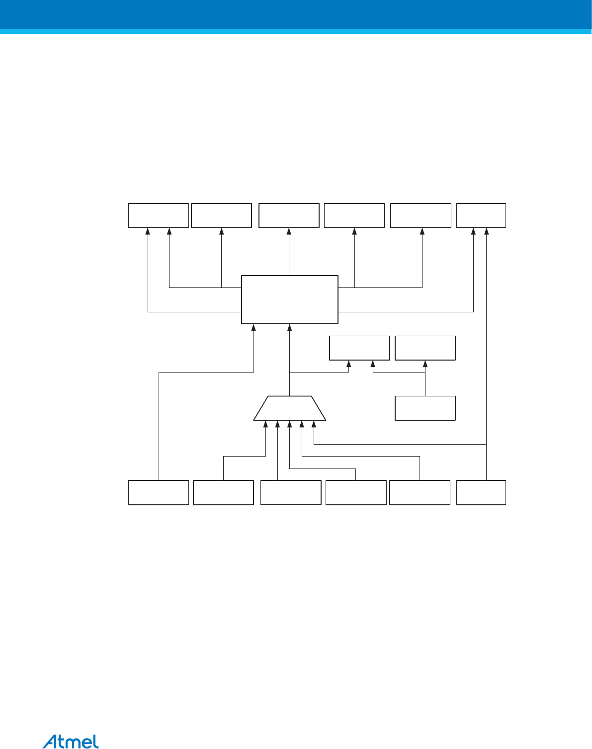
13. System Clock and Clock Options
13.1. Clock Systems and their Distribution
The figure below presents the principal clock systems in the AVR and their distribution. All of the clocks
need not be active at a given time. In order to reduce power consumption, the clocks to modules not
being used can be halted by using different sleep modes, as described in Power Management and Sleep
Modes on page 52. The clock systems are detailed in the following figure.
Figure 13-1 Clock Distribution
Gene ral I/O
Module s
Asynchronous
Timer/Counte r ADC CPU Core RAM
clkI/O
clkASY
AVR Clock
Control Unit
clkCP U
Flash a nd
EEP ROM
clkFLASH
clkADC
Source Clock
Wa tchdog Timer
Wa tchdog
Oscillator
Reset Logic
Clock
Multiplexer
Wa tchdog Clock
Calibrated RC
Oscillator
Timer/Counte r
Oscillator
Crys ta l
Oscillator
Low-Freque ncy
Crys ta l Os cilla tor
Externa l RC
Oscillator Exte rnal Clock
13.1.1. CPU Clock – clkCPU
The CPU clock is routed to parts of the system concerned with operation of the AVR core. Examples of
such modules are the General Purpose Register File, the Status Register and the Data memory holding
the Stack Pointer. Halting the CPU clock inhibits the core from performing general operations and
calculations.
13.1.2. I/O Clock – clkI/O
The I/O clock is used by the majority of the I/O modules, like Timer/Counters, SPI, and USART. The I/O
clock is also used by the External Interrupt module, but note that some external interrupts are detected by
asynchronous logic, allowing such interrupts to be detected even if the I/O clock is halted. Also note that
address recognition in the TWI module is carried out asynchronously when clkI/O is halted, enabling TWI
address reception in all sleep modes.
Atmel ATmega8A [DATASHEET]
Atmel-8159F-8-bit AVR Microcontroller_Datasheet_Complete-09/2015
44

13.1.3. Flash Clock – clkFLASH
The Flash clock controls operation of the Flash interface. The Flash clock is usually active simultaneously
with the CPU clock.
13.1.4. Asynchronous Timer Clock – clkASY
The Asynchronous Timer clock allows the Asynchronous Timer/Counter to be clocked directly from an
external 32kHz clock crystal. The dedicated clock domain allows using this Timer/Counter as a real-time
counter even when the device is in sleep mode. The Asynchronous Timer/Counter uses the same XTAL
pins as the CPU main clock but requires a CPU main clock frequency of more than four times the
Oscillator frequency. Thus, asynchronous operation is only available while the chip is clocked on the
Internal Oscillator.
13.1.5. ADC Clock – clkADC
The ADC is provided with a dedicated clock domain. This allows halting the CPU and I/O clocks in order
to reduce noise generated by digital circuitry. This gives more accurate ADC conversion results.
13.2. Clock Sources
The device has the following clock source options, selectable by Flash Fuse Bits as shown below. The
clock from the selected source is input to the AVR clock generator, and routed to the appropriate
modules.
Table 13-1 Device Clocking Options Select(1)
Device Clocking Option CKSEL3:0
External Crystal/Ceramic Resonator 1111 - 1010
External Low-frequency Crystal 1001
External RC Oscillator 1000 - 0101
Calibrated Internal RC Oscillator 0100 - 0001
External Clock 0000
Note: 1. For all fuses “1” means unprogrammed while “0” means programmed.
The various choices for each clocking option is given in the following sections. When the CPU wakes up
from Power-down or Power-save, the selected clock source is used to time the start-up, ensuring stable
Oscillator operation before instruction execution starts. When the CPU starts from reset, there is as an
additional delay allowing the power to reach a stable level before commencing normal operation. The
Watchdog Oscillator is used for timing this real-time part of the start-up time. The number of WDT
Oscillator cycles used for each time-out is shown in the table below. The frequency of the Watchdog
Oscillator is voltage dependent as shown in Typical Characteristics – TA = -40°C to 85°C. The device is
shipped with CKSEL = “0001” and SUT = “10” (1MHz Internal RC Oscillator, slowly rising power).
Table 13-2 Number of Watchdog Oscillator Cycles
Typical Time-out (VCC = 5.0V) Typical Time-out (VCC = 3.0V) Number of Cycles
4.1ms 4.3ms 4K (4,096)
65ms 69ms 64K (65,536)
Related Links
Atmel ATmega8A [DATASHEET]
Atmel-8159F-8-bit AVR Microcontroller_Datasheet_Complete-09/2015
45
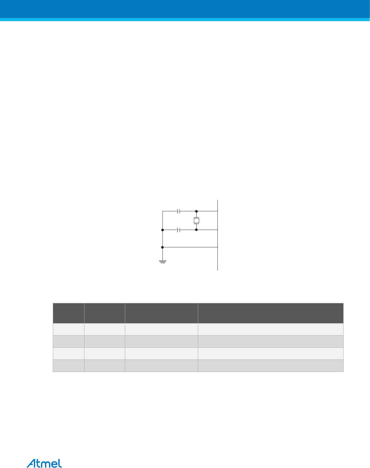
Typical Characteristics – TA = -40°C to 85°C on page 314
13.3. Crystal Oscillator
XTAL1 and XTAL2 are input and output, respectively, of an inverting amplifier which can be configured for
use as an On-chip Oscillator, as shown in the figure below. Either a quartz crystal or a ceramic resonator
may be used. The CKOPT Fuse selects between two different Oscillator amplifier modes. When CKOPT
is programmed, the Oscillator output will oscillate a full rail-to-rail swing on the output. This mode is
suitable when operating in a very noisy environment or when the output from XTAL2 drives a second
clock buffer. This mode has a wide frequency range. When CKOPT is unprogrammed, the Oscillator has
a smaller output swing. This reduces power consumption considerably. This mode has a limited
frequency range and it cannot be used to drive other clock buffers.
For resonators, the maximum frequency is 8MHz with CKOPT unprogrammed and 16MHz with CKOPT
programmed. C1 and C2 should always be equal for both crystals and resonators. The optimal value of
the capacitors depends on the crystal or resonator in use, the amount of stray capacitance, and the
electromagnetic noise of the environment. Some initial guidelines for choosing capacitors for use with
crystals are given in the next table. For ceramic resonators, the capacitor values given by the
manufacturer should be used.
Figure 13-2 Crystal Oscillator Connections
XTAL2
XTAL1
GND
C2
C1
The Oscillator can operate in three different modes, each optimized for a specific frequency range. The
operating mode is selected by the fuses CKSEL3:1 as shown in the following table.
Table 13-3 Crystal Oscillator Operating Modes
CKOPT(1) CKSEL3:1 Frequency Range(MHz) Recommended Range for Capacitors C1 and C2
for Use with Crystals (pF)
1 101(2) 0.4 - 0.9 –
1 110 0.9 - 3.0 12 - 22
1 111 3.0 - 8.0 12 - 22
0 101, 110, 111 1.0 -16.0 12 - 22
Note:
1. When CKOPT is programmed (0), the oscillator output will be a full rail-to-rail swing on the output.
2. This option should not be used with crystals, only with ceramic resonators.
The CKSEL0 Fuse together with the SUT1:0 Fuses select the start-up times as shown in the next table.
Atmel ATmega8A [DATASHEET]
Atmel-8159F-8-bit AVR Microcontroller_Datasheet_Complete-09/2015
46

Table 13-4 Start-up Times for the Crystal Oscillator Clock Selection
CKSEL0 SUT1:0 Start-up Time
from Power-down
and Power-save
Additional Delay
from Reset
(VCC = 5.0V)
Recommended Usage
0 00 258 CK(1) 4.1ms Ceramic resonator, fast rising power
0 01 258 CK(1) 65ms Ceramic resonator, slowly rising power
0 10 1K CK(2) – Ceramic resonator, BOD enabled
0 11 1K CK(2) 4.1ms Ceramic resonator, fast rising power
1 00 1K CK(2) 65ms Ceramic resonator, slowly rising power
1 01 16K CK – Crystal Oscillator, BOD enabled
1 10 16K CK 4.1ms Crystal Oscillator, fast rising power
1 11 16K CK 65ms Crystal Oscillator, slowly rising power
Note:
1. These options should only be used when not operating close to the maximum frequency of the
device, and only if frequency stability at start-up is not important for the application. These options
are not suitable for crystals.
2. These options are intended for use with ceramic resonators and will ensure frequency stability at
start-up. They can also be used with crystals when not operating close to the maximum frequency
of the device, and if frequency stability at start-up is not important for the application.
13.4. Low-frequency Crystal Oscillator
To use a 32.768kHz watch crystal as the clock source for the device, the Low-frequency Crystal Oscillator
must be selected by setting the CKSEL Fuses to “1001”. The crystal should be connected as shown in
Figure 13-2 Crystal Oscillator Connections on page 46. By programming the CKOPT Fuse, the user can
enable internal capacitors on XTAL1 and XTAL2, thereby removing the need for external capacitors. The
internal capacitors have a nominal value of 36pF.
When this Oscillator is selected, start-up times are determined by the SUT Fuses as shown in the table
below.
Table 13-5 Start-up Times for the Low-frequency Crystal Oscillator Clock Selection
SUT1:0 Start-up Time from
Power-down and
Power-save
Additional Delay
from Reset
(VCC = 5.0V)
Recommended Usage
00 1K CK(1) 4.1ms Fast rising power or BOD enabled
01 1K CK(1) 65ms Slowly rising power
10 32K CK 65ms Stable frequency at start-up
11 Reserved
Note: 1. These options should only be used if frequency stability at start-up is not important for the
application.
Atmel ATmega8A [DATASHEET]
Atmel-8159F-8-bit AVR Microcontroller_Datasheet_Complete-09/2015
47
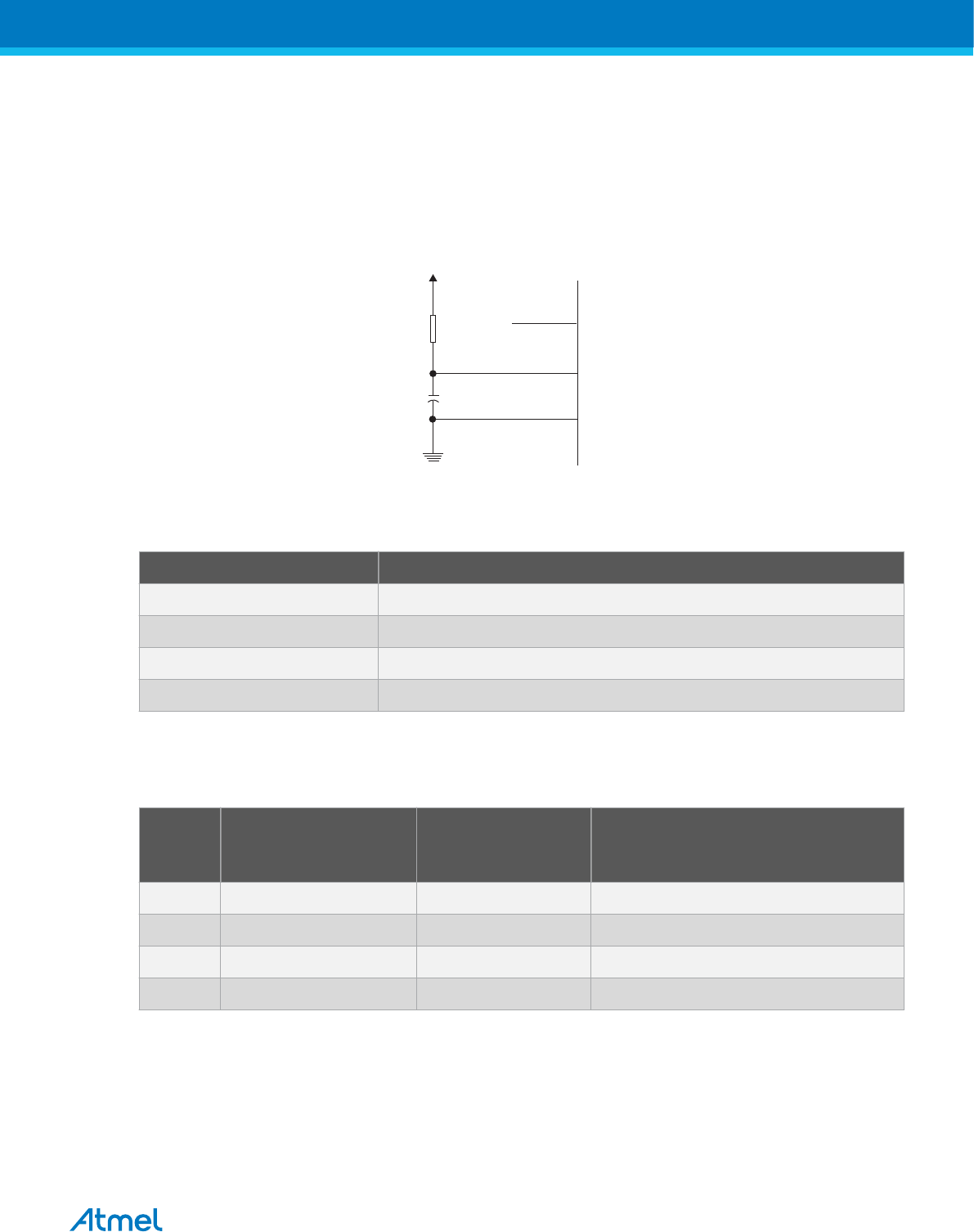
13.5. External RC Oscillator
For timing insensitive applications, the external RC configuration shown in the figure below can be used.
The frequency is roughly estimated by the equation f = 1/(3RC). C should be at least 22pF. By
programming the CKOPT Fuse, the user can enable an internal 36pF capacitor between XTAL1 and
GND, thereby removing the need for an external capacitor.
Figure 13-3 External RC Configuration
XTAL2
XTAL1
GND
C
R
VCC
NC
The Oscillator can operate in four different modes, each optimized for a specific frequency range. The
operating mode is selected by the fuses CKSEL3:0 as shown in the following table.
Table 13-6 External RC Oscillator Operating Modes
CKSEL3:0 Frequency Range (MHz)
0101 0.1 - 0.9
0110 0.9 - 3.0
0111 3.0 - 8.0
1000 8.0 - 12.0
When this Oscillator is selected, start-up times are determined by the SUT Fuses as shown in the table
below.
Table 13-7 Start-up Times for the External RC Oscillator Clock Selection
SUT1:0 Start-up Time from
Power-down and
Power-save
Additional Delay
from Reset
(VCC = 5.0V)
Recommended Usage
00 18 CK – BOD enabled
01 18 CK 4.1ms Fast rising power
10 18 CK 65ms Slowly rising power
11 6 CK(1) 4.1ms Fast rising power or BOD enabled
Note: 1. This option should not be used when operating close to the maximum frequency of the device.
13.6. Calibrated Internal RC Oscillator
The calibrated internal RC Oscillator provides a fixed 1.0, 2.0, 4.0, or 8.0MHz clock. All frequencies are
nominal values at 5V and 25°C. This clock may be selected as the system clock by programming the
CKSEL Fuses as shown in the next table. If selected, it will operate with no external components. The
Atmel ATmega8A [DATASHEET]
Atmel-8159F-8-bit AVR Microcontroller_Datasheet_Complete-09/2015
48

CKOPT Fuse should always be unprogrammed when using this clock option. During reset, hardware
loads the 1MHz calibration byte into the OSCCAL Register and thereby automatically calibrates the RC
Oscillator. At 5V, 25°C and 1.0MHz Oscillator frequency selected, this calibration gives a frequency within
± 3% of the nominal frequency. Using run-time calibration methods as described in application notes
available at www.atmel.com/avr it is possible to achieve ± 1% accuracy at any given VCC and
Temperature. When this Oscillator is used as the chip clock, the Watchdog Oscillator will still be used for
the Watchdog Timer and for the Reset Time-out. For more information on the pre-programmed calibration
value, see the section Calibration Byte.
Table 13-8 Internal Calibrated RC Oscillator Operating Modes
CKSEL3:0 Nominal Frequency (MHz)
0001(1) 1.0
0010 2.0
0011 4.0
0100 8.0
Note: 1. The device is shipped with this option selected.
When this Oscillator is selected, start-up times are determined by the SUT Fuses as shown in the table
below. PB6 (XTAL1/TOSC1) and PB7(XTAL2/TOSC2) can be used as either general I/O pins or Timer
Oscillator pins:
Table 13-9 Start-up Times for the Internal Calibrated RC Oscillator Clock Selection
SUT1:0 Start-up Time from Power-down
and Power-save
Additional Delay from Reset
(VCC = 5.0V)
Recommended Usage
00 6 CK – BOD enabled
01 6 CK 4.1ms Fast rising power
10(1) 6 CK 65ms Slowly rising power
11 Reserved
Note: 1. The device is shipped with this option selected.
Related Links
Calibration Byte on page 286
13.7. External Clock
To drive the device from an external clock source, XTAL1 should be driven as shown in the figure below.
To run the device on an external clock, the CKSEL Fuses must be programmed to “0000”. By
programming the CKOPT Fuse, the user can enable an internal 36pF capacitor between XTAL1 and
GND, and XTAL2 and GND.
Atmel ATmega8A [DATASHEET]
Atmel-8159F-8-bit AVR Microcontroller_Datasheet_Complete-09/2015
49
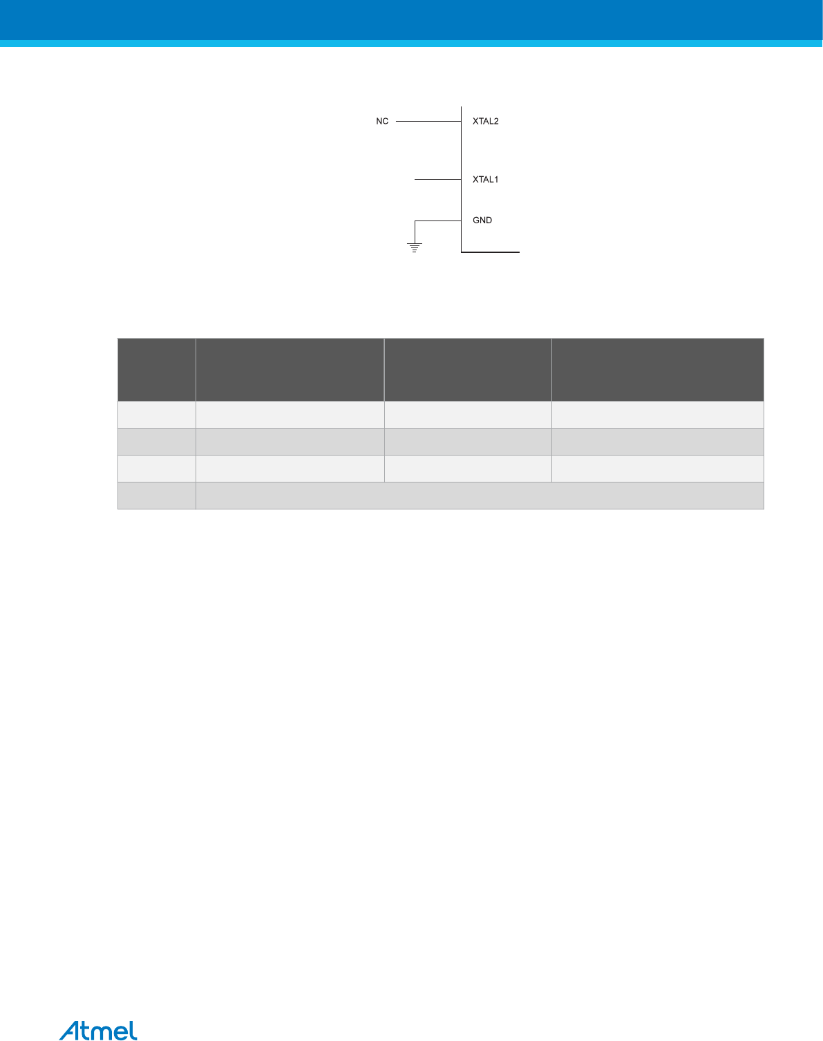
Figure 13-4 External Clock Drive Configuration
EXTERNAL
CLOCK
SIGNAL
When this clock source is selected, start-up times are determined by the SUT Fuses as shown in the
following table.
Table 13-10 Start-up Times for the External Clock Selection
SUT1:0 Start-up Time from
Power-down and
Power-save
Additional Delay
from Reset
(VCC = 5.0V)
Recommended Usage
00 6 CK – BOD enabled
01 6 CK 4.1ms Fast rising power
10 6 CK 65ms Slowly rising power
11 Reserved
When applying an external clock, it is required to avoid sudden changes in the applied clock frequency to
ensure stable operation of the MCU. A variation in frequency of more than 2% from one clock cycle to the
next can lead to unpredictable behavior. It is required to ensure that the MCU is kept in Reset during such
changes in the clock frequency.
13.8. Timer/Counter Oscillator
For AVR microcontrollers with Timer/Counter Oscillator pins (TOSC1 and TOSC2), the crystal is
connected directly between the pins. By programming the CKOPT Fuse, the user can enable internal
capacitors on XTAL1 and XTAL2, thereby removing the need for external capacitors. The Oscillator is
optimized for use with a 32.768kHz watch crystal. Applying an external clock source to TOSC1 is not
recommended.
Note: The Timer/Counter Oscillator uses the same type of crystal oscillator as Low-Frequency Oscillator
and the internal capacitors have the same nominal value of 36pF.
13.9. Register Description
Atmel ATmega8A [DATASHEET]
Atmel-8159F-8-bit AVR Microcontroller_Datasheet_Complete-09/2015
50
13.9.1. OSCCAL – The Oscillator Calibration Register
When using the I/O specific commands IN and OUT, the I/O addresses 0x00 - 0x3F must be used. When
addressing I/O Registers as data space using LD and ST instructions, 0x20 must be added to these offset
addresses. The device is a complex microcontroller with more peripheral units than can be supported
within the 64 location reserved in Opcode for the IN and OUT instructions. For the Extended I/O space
from 0x60 in SRAM, only the ST/STS/STD and LD/LDS/LDD instructions can be used.
Name: OSCCAL
Offset: 0x31
Reset: 0x00
Property:
When addressing I/O Registers as data space the offset address is 0x51
Bit 7 6 5 4 3 2 1 0
CAL7 CAL6 CAL5 CAL4 CAL3 CAL2 CAL1 CAL0
Access R/W R/W R/W R/W R/W R/W R/W R/W
Reset x x x x x x x x
Bits 7:0 – CALn: Oscillator Calibration Value [n = 7:0]
Writing the calibration byte to this address will trim the Internal Oscillator to remove process variations
from the Oscillator frequency. During Reset, the 1MHz calibration value which is located in the signature
row High byte (address 0x00) is automatically loaded into the OSCCAL Register. If the internal RC is
used at other frequencies, the calibration values must be loaded manually. This can be done by first
reading the signature row by a programmer, and then store the calibration values in the Flash or
EEPROM. Then the value can be read by software and loaded into the OSCCAL Register. When
OSCCAL is zero, the lowest available frequency is chosen. Writing non-zero values to this register will
increase the frequency of the Internal Oscillator. Writing 0xFF to the register gives the highest available
frequency. The calibrated Oscillator is used to time EEPROM and Flash access. If EEPROM or Flash is
written, do not calibrate to more than 10% above the nominal frequency. Otherwise, the EEPROM or
Flash write may fail. Note that the Oscillator is intended for calibration to 1.0, 2.0, 4.0, or 8.0MHz. Tuning
to other values is not guaranteed, as indicated in the following table.
Note: The OSCCAL reset value is the device specific calibration value.
Table 13-11 Internal RC Oscillator Frequency Range
OSCCAL Value Min Frequency in Percentage of
Nominal Frequency (%)
Max Frequency in Percentage of
Nominal Frequency (%)
0x00 50 100
0x7F 75 150
0xFF 100 200
Atmel ATmega8A [DATASHEET]
Atmel-8159F-8-bit AVR Microcontroller_Datasheet_Complete-09/2015
51

14. Power Management and Sleep Modes
14.1. Sleep Modes
Sleep modes enable the application to shut down unused modules in the MCU, thereby saving power.
The AVR provides various sleep modes allowing the user to tailor the power consumption to the
application’s requirements.
Figure Clock Distribution in section Clock Systems and their Distribution presents the different clock
systems in the ATmega8A, and their distribution. The figure is helpful in selecting an appropriate sleep
mode. The table below shows the different clock options and their wake-up sources.
Table 14-1 Active Clock Domains and Wake-up Sources in the Different Sleep Modes
Active Clock Domains Oscillators Wake-up Sources
Sleep
Mode
clkCPU clkFLASH clkIO clkADC clkASY Main
Clock
Source
Enabled
Timer
Osc.
Enabled
INT1/
INT0
TWIAddress
Match
Timer2 SPM/
EEPROM
Ready
ADC Other
I/O
Idle X X X X X(2) X X X X X X
ADC
Noise
Reduction
X X X X(2) X(3) X X X X
Power-
down
X(3) X
Power-
save
X(2) X(2) X(3) X X(2)
Standby(1
)X X(3) X
Note:
1. External Crystal or resonator selected as clock source.
2. If AS2 bit in ASSR is set.
3. Only level interrupt INT1 and INT0.
To enter any of the five sleep modes, the SE bit in MCUCR must be written to logic one and a SLEEP
instruction must be executed. The SM2, SM1, and SM0 bits in the MCUCR Register select which sleep
mode (Idle, ADC Noise Reduction, Power-down, Power-save, or Standby) will be activated by the SLEEP
instruction. See the table above for a summary.
If an enabled interrupt occurs while the MCU is in a sleep mode, the MCU wakes up. The MCU is then
halted for four cycles in addition to the start-up time, it executes the interrupt routine, and resumes
execution from the instruction following SLEEP. The contents of the Register File and SRAM are
unaltered when the device wakes up from sleep. If a reset occurs during sleep mode, the MCU wakes up
and executes from the Reset Vector.
Note that the Extended Standby mode present in many other AVR MCUs has been removed in the
ATmega8A, as the TOSC and XTAL inputs share the same physical pins.
Related Links
Clock Systems and their Distribution on page 44
Atmel ATmega8A [DATASHEET]
Atmel-8159F-8-bit AVR Microcontroller_Datasheet_Complete-09/2015
52

14.2. Idle Mode
When the SM2:0 bits are written to 000, the SLEEP instruction makes the MCU enter Idle mode, stopping
the CPU but allowing SPI, USART, Analog Comparator, ADC, Two-wire Serial Interface, Timer/Counters,
Watchdog, and the interrupt system to continue operating. This sleep mode basically halts clkCPU and
clkFLASH, while allowing the other clocks to run.
Idle mode enables the MCU to wake up from external triggered interrupts as well as internal ones like the
Timer Overflow and USART Transmit Complete interrupts. If wake-up from the Analog Comparator
interrupt is not required, the Analog Comparator can be powered down by setting the ACD bit in the
Analog Comparator Control and Status Register – ACSR. This will reduce power consumption in Idle
mode. If the ADC is enabled, a conversion starts automatically when this mode is entered.
14.3. ADC Noise Reduction Mode
When the SM2:0 bits are written to 001, the SLEEP instruction makes the MCU enter ADC Noise
Reduction mode, stopping the CPU but allowing the ADC, the external interrupts, the Two-wire Serial
Interface address watch, Timer/Counter2 and the Watchdog to continue operating (if enabled). This sleep
mode basically halts clkI/O, clkCPU, and clkFLASH, while allowing the other clocks to run.
This improves the noise environment for the ADC, enabling higher resolution measurements. If the ADC
is enabled, a conversion starts automatically when this mode is entered. Apart form the ADC Conversion
Complete interrupt, only an External Reset, a Watchdog Reset, a Brown-out Reset, a Two-wire Serial
Interface address match interrupt, a Timer/Counter2 interrupt, an SPM/EEPROM ready interrupt, or an
external level interrupt on INT0 or INT1, can wake up the MCU from ADC Noise Reduction mode.
14.4. Power-down Mode
When the SM2:0 bits are written to 010, the SLEEP instruction makes the MCU enter Power-down mode.
In this mode, the External Oscillator is stopped, while the external interrupts, the Two-wire Serial Interface
address watch, and the Watchdog continue operating (if enabled). Only an External Reset, a Watchdog
Reset, a Brown-out Reset, a Two-wire Serial Interface address match interrupt, or an external level
interrupt on INT0 or INT1, can wake up the MCU. This sleep mode basically halts all generated clocks,
allowing operation of asynchronous modules only.
Note that if a level triggered interrupt is used for wake-up from Power-down mode, the changed level
must be held for some time to wake up the MCU. Refer to External Interrupts for details.
When waking up from Power-down mode, there is a delay from the wake-up condition occurs until the
wake-up becomes effective. This allows the clock to restart and become stable after having been
stopped. The wake-up period is defined by the same CKSEL Fuses that define the Reset Time-out
period, as described in Clock Sources.
Related Links
External Interrupts on page 73
Clock Sources on page 45
14.5. Power-save Mode
When the SM2:0 bits are written to 011, the SLEEP instruction makes the MCU enter Power-save mode.
This mode is identical to Power-down, with one exception:
Atmel ATmega8A [DATASHEET]
Atmel-8159F-8-bit AVR Microcontroller_Datasheet_Complete-09/2015
53

•If Timer/Counter2 is clocked asynchronously, i.e. the AS2 bit in ASSR is set, Timer/Counter2 will
run during sleep. The device can wake up from either Timer Overflow or Output Compare event
from Timer/Counter2 if the corresponding Timer/Counter2 interrupt enable bits are set in TIMSK,
and the global interrupt enable bit in SREG is set.
If the asynchronous timer is NOT clocked asynchronously, Power-down mode is recommended instead of
Power-save mode because the contents of the registers in the asynchronous timer should be considered
undefined after wake-up in Power-save mode if AS2 is 0.
This sleep mode basically halts all clocks except clkASY, allowing operation only of asynchronous
modules, including Timer/Counter2 if clocked asynchronously.
14.6. Standby Mode
When the SM2:0 bits are 110 and an external crystal/resonator clock option is selected, the SLEEP
instruction makes the MCU enter Standby mode. This mode is identical to Power-down with the exception
that the Oscillator is kept running. From Standby mode, the device wakes up in 6 clock cycles.
14.7. Minimizing Power Consumption
There are several issues to consider when trying to minimize the power consumption in an AVR
controlled system. In general, sleep modes should be used as much as possible, and the sleep mode
should be selected so that as few as possible of the device’s functions are operating. All functions not
needed should be disabled. In particular, the following modules may need special consideration when
trying to achieve the lowest possible power consumption.
14.7.1. Analog-to-Digital Converter (ADC)
If enabled, the ADC will be enabled in all sleep modes. To save power, the ADC should be disabled
before entering any sleep mode. When the ADC is turned off and on again, the next conversion will be an
extended conversion. Refer to Analog-to-Digital Converter for details on ADC operation.
Related Links
ADC - Analog to Digital Converter on page 248
14.7.2. Analog Comparator
When entering Idle mode, the Analog Comparator should be disabled if not used. When entering ADC
Noise Reduction mode, the Analog Comparator should be disabled. In the other sleep modes, the Analog
Comparator is automatically disabled. However, if the Analog Comparator is set up to use the Internal
Voltage Reference as input, the Analog Comparator should be disabled in all sleep modes. Otherwise,
the Internal Voltage Reference will be enabled, independent of sleep mode. Refer to Analog Comparator
for details on how to configure the Analog Comparator.
Related Links
Analog Comparator on page 243
14.7.3. Brown-out Detector
If the Brown-out Detector is not needed in the application, this module should be turned off. If the Brown-
out Detector is enabled by the BODEN Fuse, it will be enabled in all sleep modes, and hence, always
consume power. In the deeper sleep modes, this will contribute significantly to the total current
consumption. Refer to Brown-out Detection for details on how to configure the Brown-out Detector.
Related Links
Brown-out Detection on page 59
Atmel ATmega8A [DATASHEET]
Atmel-8159F-8-bit AVR Microcontroller_Datasheet_Complete-09/2015
54

14.7.4. Internal Voltage Reference
The Internal Voltage Reference will be enabled when needed by the Brown-out Detector, the Analog
Comparator or the ADC. If these modules are disabled as described in the sections above, the internal
voltage reference will be disabled and it will not be consuming power. When turned on again, the user
must allow the reference to start up before the output is used. If the reference is kept on in sleep mode,
the output can be used immediately. Refer to Internal Voltage Reference for details on the start-up time.
Related Links
Internal Voltage Reference on page 60
14.7.5. Watchdog Timer
If the Watchdog Timer is not needed in the application, this module should be turned off. If the Watchdog
Timer is enabled, it will be enabled in all sleep modes, and hence, always consume power. In the deeper
sleep modes, this will contribute significantly to the total current consumption. Refer to Watchdog Timer
for details on how to configure the Watchdog Timer.
Related Links
Watchdog Timer on page 61
14.7.6. Port Pins
When entering a sleep mode, all port pins should be configured to use minimum power. The most
important thing is then to ensure that no pins drive resistive loads. In sleep modes where the both the I/O
clock (clkI/O) and the ADC clock (clkADC) are stopped, the input buffers of the device will be disabled. This
ensures that no power is consumed by the input logic when not needed. In some cases, the input logic is
needed for detecting wake-up conditions, and it will then be enabled. Refer to the section Digital Input
Enable and Sleep Modes for details on which pins are enabled. If the input buffer is enabled and the input
signal is left floating or have an analog signal level close to VCC/2, the input buffer will use excessive
power.
Related Links
Digital Input Enable and Sleep Modes on page 81
14.8. Register Description
Atmel ATmega8A [DATASHEET]
Atmel-8159F-8-bit AVR Microcontroller_Datasheet_Complete-09/2015
55
14.8.1. MCUCR – MCU Control Register
The MCU Control Register contains control bits for power management.
When using the I/O specific commands IN and OUT, the I/O addresses 0x00 - 0x3F must be used. When
addressing I/O Registers as data space using LD and ST instructions, 0x20 must be added to these offset
addresses. The device is a complex microcontroller with more peripheral units than can be supported
within the 64 location reserved in Opcode for the IN and OUT instructions. For the Extended I/O space
from 0x60 in SRAM, only the ST/STS/STD and LD/LDS/LDD instructions can be used.
Name: MCUCR
Offset: 0x35
Reset: 0x00
Property:
When addressing I/O Registers as data space the offset address is 0x55
Bit 7 6 5 4 3 2 1 0
SE SM2 SM1 SM0
Access R/W R/W R/W R/W
Reset 0 0 0 0
Bit 5 – SE: Sleep Enable
The SE bit must be written to logic one to make the MCU enter the sleep mode when the SLEEP
instruction is executed. To avoid the MCU entering the sleep mode unless it is the programmer’s purpose,
it is recommended to set the Sleep Enable (SE) bit just before the execution of the SLEEP instruction.
Bits 4:2 – SMn: Sleep Mode n Select Bits [n=2:0]
These bits select between the five available sleep modes as shown in the table.
SM2 SM1 SM0 Sleep Mode
0 0 0 Idle
0 0 1 ADC Noise Reduction
0 1 0 Power-down
0 1 1 Power-save
1 0 0 Reserved
1 0 1 Reserved
1 1 0 Standby(1)
Note: 1. Standby mode is only available with external crystals or resonators.
Atmel ATmega8A [DATASHEET]
Atmel-8159F-8-bit AVR Microcontroller_Datasheet_Complete-09/2015
56

15. System Control and Reset
15.1. Resetting the AVR
During Reset, all I/O Registers are set to their initial values, and the program starts execution from the
Reset Vector. If the program never enables an interrupt source, the Interrupt Vectors are not used, and
regular program code can be placed at these locations. This is also the case if the Reset Vector is in the
Application section while the Interrupt Vectors are in the boot section or vice versa. The circuit diagram in
the following section shows the Reset Logic. The Table in System and Reset Characteristics defines the
electrical parameters of the reset circuitry.
The I/O ports of the AVR are immediately reset to their initial state when a reset source goes active. This
does not require any clock source to be running.
After all reset sources have gone inactive, a delay counter is invoked, stretching the internal reset. This
allows the power to reach a stable level before normal operation starts. The time-out period of the delay
counter is defined by the user through the CKSEL Fuses. The different selections for the delay period are
presented in Clock Sources.
Related Links
System and Reset Characteristics on page 305
Clock Sources on page 45
15.2. Reset Sources
The ATmega8A has four sources of Reset:
•Power-on Reset. The MCU is reset when the supply voltage is below the Power-on Reset threshold
(VPOT).
•External Reset. The MCU is reset when a low level is present on the RESET pin for longer than the
minimum pulse length.
•Watchdog Reset. The MCU is reset when the Watchdog Timer period expires and the Watchdog is
enabled.
•Brown-out Reset. The MCU is reset when the supply voltage VCC is below the Brown-out Reset
threshold (VBOT) and the Brown-out Detector is enabled.
Atmel ATmega8A [DATASHEET]
Atmel-8159F-8-bit AVR Microcontroller_Datasheet_Complete-09/2015
57
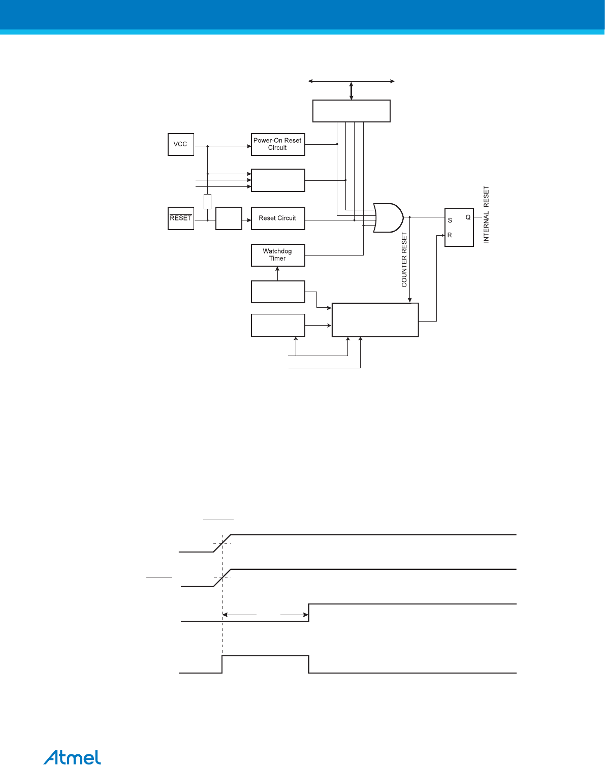
Figure 15-1 Reset Logic
MCU Control a nd S ta tus
Register (MCUCS R)
Brown-Out
Reset Circuit
BODEN
BODLEVEL
Delay Counters
CKSEL[3:0]
CK
TIMEOUT
WDRF
BORF
EXTRF
PORF
DATA BUS
Clock
Generator
SPIKE
FILTER
Pull-up Re s is tor
Wa tchdog
Oscillator
SUT[1:0]
15.2.1. Power-on Reset
A Power-on Reset (POR) pulse is generated by an On-chip detection circuit. The detection level is
defined in the table in System and Reset Characteristics. The POR is activated whenever VCC is below
the detection level. The POR circuit can be used to trigger the Start-up Reset, as well as to detect a
failure in supply voltage.
A Power-on Reset (POR) circuit ensures that the device is reset from Power-on. Reaching the Power-on
Reset threshold voltage invokes the delay counter, which determines how long the device is kept in
RESET after VCC rise. The RESET signal is activated again, without any delay, when VCC decreases
below the detection level.
Figure 15-2 MCU Start-up, RESET Tied to VCC
V
RES ET
TIME-OUT
INTERNAL
RES ET
tTOUT
VPOT
VRST
CC
Atmel ATmega8A [DATASHEET]
Atmel-8159F-8-bit AVR Microcontroller_Datasheet_Complete-09/2015
58
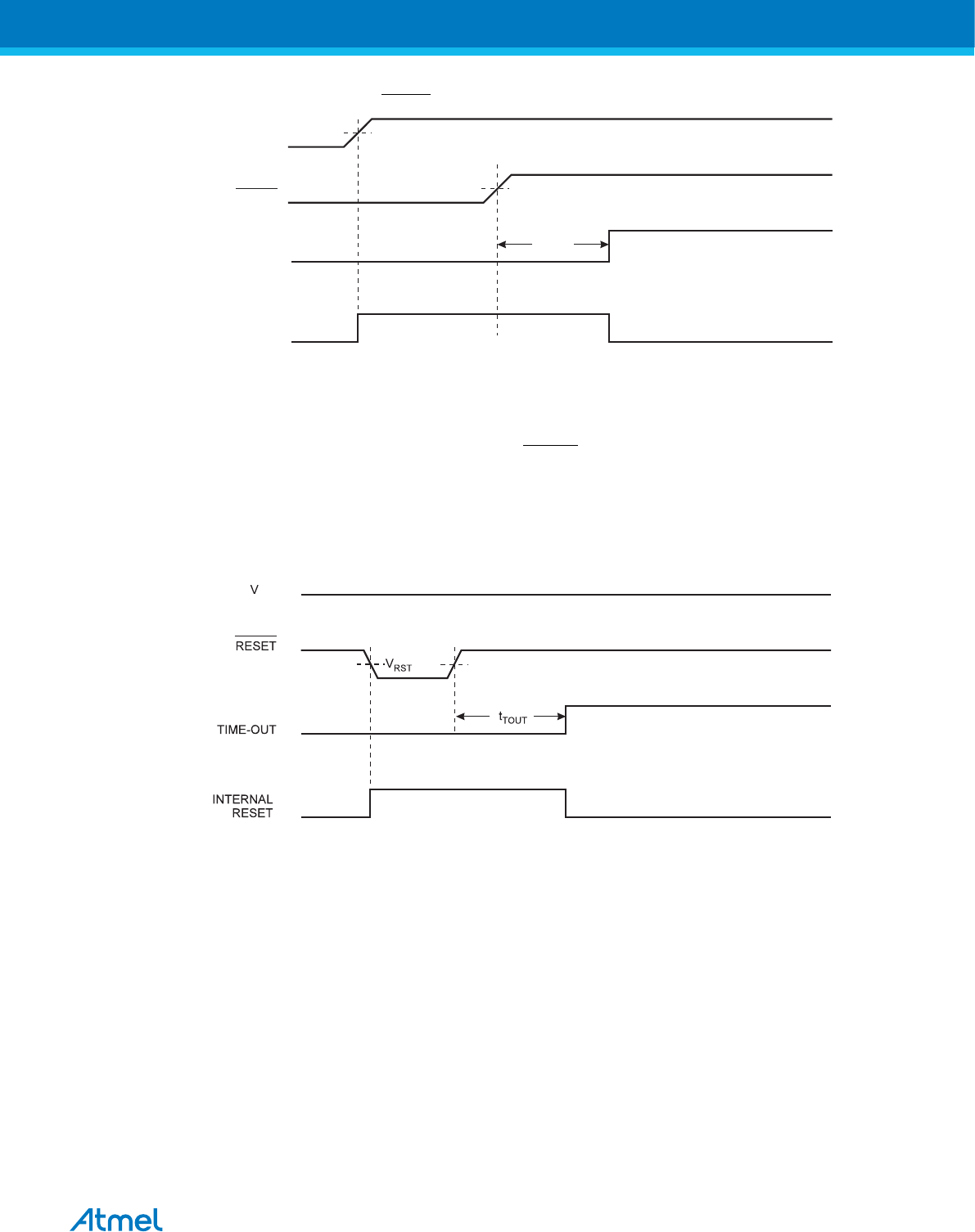
Figure 15-3 Figure: MCU Start-up, RESET Extended Externally
RES ET
TIME-OUT
INTERNAL
RES ET
tTOUT
VPOT
VRST
VCC
Related Links
System and Reset Characteristics on page 305
15.2.2. External Reset
An External Reset is generated by a low level on the RESET pin. Reset pulses longer than the minimum
pulse width (see table in System and Reset Characteristics) will generate a reset, even if the clock is not
running. Shorter pulses are not guaranteed to generate a reset. When the applied signal reaches the
Reset Threshold Voltage – VRST on its positive edge, the delay counter starts the MCU after the time-out
period tTOUT has expired.
Figure 15-4 External Reset During Operation
CC
Related Links
System and Reset Characteristics on page 305
15.2.3. Brown-out Detection
ATmega8A has an On-chip Brown-out Detection (BOD) circuit for monitoring the VCC level during
operation by comparing it to a fixed trigger level. The trigger level for the BOD can be selected by the fuse
BODLEVEL to be 2.7V (BODLEVEL unprogrammed), or 4.0V (BODLEVEL programmed). The trigger
level has a hysteresis to ensure spike free Brown-out Detection. The hysteresis on the detection level
should be interpreted as VBOT+ = VBOT + VHYST/2 and VBOT- = VBOT - VHYST/2.
The BOD circuit can be enabled/disabled by the fuse BODEN. When the BOD is enabled (BODEN
programmed), and VCC decreases to a value below the trigger level (VBOT- in the figure below), the
Brown-out Reset is immediately activated. When VCC increases above the trigger level (VBOT+ in the
figure below), the delay counter starts the MCU after the time-out period tTOUT has expired.
The BOD circuit will only detect a drop in VCC if the voltage stays below the trigger level for longer than
tBOD given in the table in System and Reset Characteristics.
Atmel ATmega8A [DATASHEET]
Atmel-8159F-8-bit AVR Microcontroller_Datasheet_Complete-09/2015
59
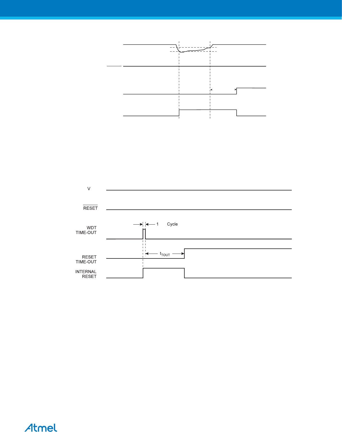
Figure 15-5 Brown-out Reset During Operation
VCC
RES ET
TIME-OUT
INTERNAL
RES ET
VBOT-
VBOT+
tTOUT
Related Links
System and Reset Characteristics on page 305
15.2.4. Watchdog Reset
When the Watchdog times out, it will generate a short reset pulse of 1 CK cycle duration. On the falling
edge of this pulse, the delay timer starts counting the time-out period tTOUT. Refer to Watchdog Timer on
page 61 for details on operation of the Watchdog Timer.
Figure 15-6 Watchdog Reset During Operation
CK
CC
15.3. Internal Voltage Reference
ATmega8A features an internal bandgap reference. This reference is used for Brown-out Detection, and it
can be used as an input to the Analog Comparator or the ADC. The 2.56V reference to the ADC is
generated from the internal bandgap reference.
15.3.1. Voltage Reference Enable Signals and Start-up Time
The voltage reference has a start-up time that may influence the way it should be used. The start-up time
is given in the table in System and Reset Characteristics. To save power, the reference is not always
turned on. The reference is on during the following situations:
1. When the BOD is enabled (by programming the BODEN Fuse).
2. When the bandgap reference is connected to the Analog Comparator (by setting the ACBG bit in
ACSR).
3. When the ADC is enabled.
Atmel ATmega8A [DATASHEET]
Atmel-8159F-8-bit AVR Microcontroller_Datasheet_Complete-09/2015
60
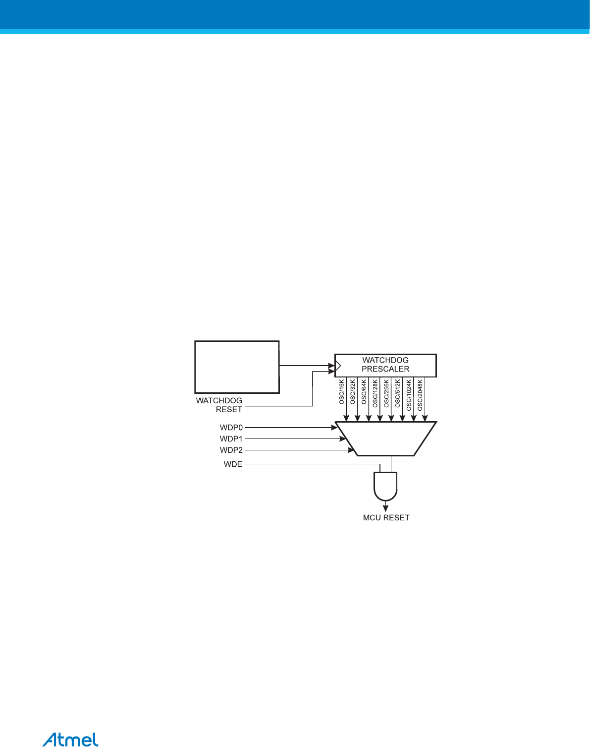
Thus, when the BOD is not enabled, after setting the ACBG bit or enabling the ADC, the user must
always allow the reference to start up before the output from the Analog Comparator or ADC is used. To
reduce power consumption in Power-down mode, the user can avoid the three conditions above to
ensure that the reference is turned off before entering Power-down mode.
Related Links
System and Reset Characteristics on page 305
15.4. Watchdog Timer
The Watchdog Timer is clocked from a separate On-chip Oscillator which runs at 1MHz. This is the typical
value at VCC = 5V. See characterization data for typical values at other VCC levels. By controlling the
Watchdog Timer prescaler, the Watchdog Reset interval can be adjusted as shown in the figure below.
The WDR – Watchdog Reset – instruction resets the Watchdog Timer. The Watchdog Timer is also reset
when it is disabled and when a Chip Reset occurs. Eight different clock cycle periods can be selected to
determine the reset period. If the reset period expires without another Watchdog Reset, the ATmega8A
resets and executes from the Reset Vector. For timing details on the Watchdog Reset, refer to Watchdog
Reset on page 60.
To prevent unintentional disabling of the Watchdog, a special turn-off sequence must be followed when
the Watchdog is disabled. Refer to the description of the Watchdog Timer Control Register for details.
Figure 15-7 Watchdog Timer
WATCHDOG
OS CILLATOR
15.5. Timed Sequences for Changing the Configuration of the Watchdog Timer
The sequence for changing the Watchdog Timer configuration differs slightly between the safety levels.
Separate procedures are described for each level.
Atmel ATmega8A [DATASHEET]
Atmel-8159F-8-bit AVR Microcontroller_Datasheet_Complete-09/2015
61

Assembly Code Example
WDT_off:
; reset WDT
WDR
; Write logical one to WDCE and WDE
in r16, WDTCR
ori r16, (1<<WDCE)|(1<<WDE)
out WDTCR, r16
; Turn off WDT
ldi r16, (0<<WDE)
out WDTCR, r16
ret
C Code Example
void WDT_off(void)
{
/* reset WDT */
_WDR();
/* Write logical one to WDCE and WDE */
WDTCR |= (1<<WDCE) | (1<<WDE);
/* Turn off WDT */
WDTCR = 0x00;
}
15.5.1. Safety Level 1 (WDTON Fuse Unprogrammed)
In this mode, the Watchdog Timer is initially disabled, but can be enabled by writing the WDE bit to 1
without any restriction. A timed sequence is needed when changing the Watchdog Time-out period or
disabling an enabled Watchdog Timer. To disable an enabled Watchdog Timer and/or changing the
Watchdog Time-out, the following procedure must be followed:
1. In the same operation, write a logic one to WDCE and WDE. A logic one must be written to WDE
regardless of the previous value of the WDE bit.
2. Within the next four clock cycles, in the same operation, write the WDE and WDP bits as desired,
but with the WDCE bit cleared.
15.5.2. Safety Level 2 (WDTON Fuse Programmed)
In this mode, the Watchdog Timer is always enabled, and the WDE bit will always read as one. A timed
sequence is needed when changing the Watchdog Time-out period. To change the Watchdog Time-out,
the following procedure must be followed:
1. In the same operation, write a logical one to WDCE and WDE. Even though the WDE always is set,
the WDE must be written to one to start the timed sequence.
Within the next four clock cycles, in the same operation, write the WDP bits as desired, but with the
WDCE bit cleared. The value written to the WDE bit is irrelevant.
15.6. Register Description
Atmel ATmega8A [DATASHEET]
Atmel-8159F-8-bit AVR Microcontroller_Datasheet_Complete-09/2015
62
15.6.1. MCUCSR – MCU Control and Status Register
The MCU Control and Status Register provides information on which reset source caused an MCU Reset.
When using the I/O specific commands IN and OUT, the I/O addresses 0x00 - 0x3F must be used. When
addressing I/O Registers as data space using LD and ST instructions, 0x20 must be added to these offset
addresses. The device is a complex microcontroller with more peripheral units than can be supported
within the 64 location reserved in Opcode for the IN and OUT instructions. For the Extended I/O space
from 0x60 in SRAM, only the ST/STS/STD and LD/LDS/LDD instructions can be used.
.
Name: MCUCSR
Offset: 0x34
Reset: 0x00
Property:
When addressing I/O Registers as data space the offset address is 0x54
Bit 7 6 5 4 3 2 1 0
WDRF BORF EXTRF PORF
Access R/W R/W R/W R/W
Reset 0 0 0 0
Bit 3 – WDRF: Watchdog Reset Flag
This bit is set if a Watchdog Reset occurs. The bit is reset by a Power-on Reset, or by writing a logic zero
to the flag.
Bit 2 – BORF: Brown-out Reset Flag
This bit is set if a Brown-out Reset occurs. The bit is reset by a Power-on Reset, or by writing a logic zero
to the flag.
Bit 1 – EXTRF: External Reset Flag
This bit is set if an External Reset occurs. The bit is reset by a Power-on Reset, or by writing a logic zero
to the flag.
Bit 0 – PORF: Power-on Reset Flag
This bit is set if a Power-on Reset occurs. The bit is reset only by writing a logic zero to the flag. To make
use of the Reset Flags to identify a reset condition, the user should read and then reset the MCUCSR as
early as possible in the program. If the register is cleared before another reset occurs, the source of the
reset can be found by examining the Reset Flags.
Atmel ATmega8A [DATASHEET]
Atmel-8159F-8-bit AVR Microcontroller_Datasheet_Complete-09/2015
63
15.6.2. WDTCR – Watchdog Timer Control Register
When using the I/O specific commands IN and OUT, the I/O addresses 0x00 - 0x3F must be used. When
addressing I/O Registers as data space using LD and ST instructions, 0x20 must be added to these offset
addresses. The device is a complex microcontroller with more peripheral units than can be supported
within the 64 location reserved in Opcode for the IN and OUT instructions. For the Extended I/O space
from 0x60 in SRAM, only the ST/STS/STD and LD/LDS/LDD instructions can be used.
Name: WDTCR
Offset: 0x21
Reset: 0x00
Property:
When addressing I/O Registers as data space the offset address is 0x41
Bit 7 6 5 4 3 2 1 0
WDCE WDE WDP2 WDP1 WDP0
Access R/W R/W R/W R/W R/W
Reset 0 0 0 0 0
Bit 4 – WDCE: Watchdog Change Enable
This bit must be set when the WDE bit is written to logic zero. Otherwise, the Watchdog will not be
disabled. Once written to one, hardware will clear this bit after four clock cycles. Refer to the description
of the WDE bit for a Watchdog disable procedure. In Safety Level 1 and 2, this bit must also be set when
changing the prescaler bits. See Code Examples.
Bit 3 – WDE: Watchdog Enable
When the WDE is written to logic one, the Watchdog Timer is enabled, and if the WDE is written to logic
zero, the Watchdog Timer function is disabled. WDE can only be cleared if the WDCE bit has logic level
one. To disable an enabled Watchdog Timer, the following procedure must be followed:
1. In the same operation, write a logic one to WDCE and WDE. A logic one must be written to WDE
even though it is set to one before the disable operation starts.
2. Within the next four clock cycles, write a logic 0 to WDE. This disables the Watchdog.
Bits 2:0 – WDPn: Watchdog Timer Prescaler 2, 1, and 0 [n = 2:0]
The WDP2, WDP1, and WDP0 bits determine the Watchdog Timer prescaling when the Watchdog Timer
is enabled. The different prescaling values and their corresponding Timeout Periods are shown in the
table below.
Table 15-1 Watchdog Timer Prescale Select
WDP2 WDP1 WDP0 Number of WDT Oscillator
Cycles
Typical
Time-out at
VCC = 3.0V
Typical
Time-out at
VCC = 5.0V
0 0 0 16K (16,384) 17.1ms 16.3ms
0 0 1 32K (32,768) 34.3ms 32.5ms
0 1 0 64K (65,536) 68.5ms 65ms
0 1 1 128K (131,072) 0.14s 0.13s
1 0 0 256K (262,144) 0.27s 0.26s
1 0 1 512K (524,288) 0.55s 0.52s
Atmel ATmega8A [DATASHEET]
Atmel-8159F-8-bit AVR Microcontroller_Datasheet_Complete-09/2015
64

WDP2 WDP1 WDP0 Number of WDT Oscillator
Cycles
Typical
Time-out at
VCC = 3.0V
Typical
Time-out at
VCC = 5.0V
1 1 0 1,024K (1,048,576) 1.1s 1.0s
1 1 1 2,048K (2,097,152) 2.2s 2.1s
Atmel ATmega8A [DATASHEET]
Atmel-8159F-8-bit AVR Microcontroller_Datasheet_Complete-09/2015
65

16. Interrupts
This section describes the specifics of the interrupt handling performed by the ATmega8A. For a general
explanation of the AVR interrupt handling, refer to Reset and Interrupt Handling.
Related Links
Reset and Interrupt Handling on page 31
16.1. Interrupt Vectors in ATmega8A
Table 16-1 Reset and Interrupt Vectors
Vector No. Program
Address(2)
Source Interrupt Definition
1 0x000(1) RESET External Pin, Power-on Reset, Brown-out Reset, and
Watchdog Reset
2 0x001 INT0 External Interrupt Request 0
3 0x002 INT1 External Interrupt Request 1
4 0x003 TIMER2 COMP Timer/Counter2 Compare Match
5 0x004 TIMER2 OVF Timer/Counter2 Overflow
6 0x005 TIMER1 CAPT Timer/Counter1 Capture Event
7 0x006 TIMER1 COMPA Timer/Counter1 Compare Match A
8 0x007 TIMER1 COMPB Timer/Counter1 Compare Match B
9 0x008 TIMER1 OVF Timer/Counter1 Overflow
10 0x009 TIMER0 OVF Timer/Counter0 Overflow
11 0x00A SPI, STC Serial Transfer Complete
12 0x00B USART, RXC USART, Rx Complete
13 0x00C USART, UDRE USART Data Register Empty
14 0x00D USART, TXC USART, Tx Complete
15 0x00E ADC ADC Conversion Complete
16 0x00F EE_RDY EEPROM Ready
17 0x010 ANA_COMP Analog Comparator
18 0x011 TWI Two-wire Serial Interface
19 0x012 SPM_RDY Store Program Memory Ready
Note:
1. When the BOOTRST Fuse is programmed, the device will jump to the Boot Loader address at
reset, see Boot Loader Support – Read-While-Write Self-Programming.
2. When the IVSEL bit in GICR is set, Interrupt Vectors will be moved to the start of the boot Flash
section. The address of each Interrupt Vector will then be the address in this table added to the
start address of the boot Flash section.
Atmel ATmega8A [DATASHEET]
Atmel-8159F-8-bit AVR Microcontroller_Datasheet_Complete-09/2015
66

The next table shows reset and Interrupt Vectors placement for the various combinations of BOOTRST
and IVSEL settings. If the program never enables an interrupt source, the Interrupt Vectors are not used,
and regular program code can be placed at these locations. This is also the case if the Reset Vector is in
the Application section while the Interrupt Vectors are in the boot section or vice versa.
Table 16-2 Reset and Interrupt Vectors Placement
BOOTRST(1) IVSEL Reset Address Interrupt Vectors Start Address
1 0 0x000 0x001
1 1 0x000 Boot Reset Address + 0x001
0 0 Boot Reset Address 0x001
0 1 Boot Reset Address Boot Reset Address + 0x001
Note: 1. The Boot Reset Address is shown in table Boot Size Configuration in the Boot Loader
Parameters section. For the BOOTRST Fuse “1” means unprogrammed while “0” means programmed.
The most typical and general program setup for the Reset and Interrupt Vector Addresses in ATmega8A
is:
address Labels Code Comments
$000 rjmp RESET ; Reset Handler
$001 rjmp EXT_INT0 ; IRQ0 Handler
$002 rjmp EXT_INT1 ; IRQ1 Handler
$003 rjmp TIM2_COMP ; Timer2 Compare
Handler
$004 rjmp TIM2_OVF ; Timer2 Overflow
Handler
$005 rjmp TIM1_CAPT ; Timer1 Capture
Handler
$006 rjmp TIM1_COMPA ; Timer1 CompareA
Handler
$007 rjmp TIM1_COMPB ; Timer1 CompareB
Handler
$008 rjmp TIM1_OVF ; Timer1 Overflow
Handler
$009 rjmp TIM0_OVF ; Timer0 Overflow
Handler
$00a rjmp SPI_STC ; SPI Transfer
Complete Handler
$00b rjmp USART_RXC ; USART RX
Complete Handler
$00c rjmp USART_UDRE ; UDR Empty
Handler
Atmel ATmega8A [DATASHEET]
Atmel-8159F-8-bit AVR Microcontroller_Datasheet_Complete-09/2015
67

address Labels Code Comments
$00d rjmp USART_TXC ; USART TX
Complete Handler
$00e rjmp ADC ; ADC Conversion
Complete Handler
$00f rjmp EE_RDY ; EEPROM Ready
Handler
$010 rjmp ANA_COMP ; Analog
Comparator Handler
$011 rjmp TWSI ; Two-wire Serial
Interface Handler
$012 rjmp SPM_RDY ; Store Program
Memory Ready
Handler
;
$013 RESET: ldi r16,high(RAMEND) ; Main program
start
$014 out SPH,r16$013 ; Set Stack
Pointer to top of
RAM
$015 ldi r16,low(RAMEND)
$013
$016 out SPL,r16$013
$017 sei ; Enable
interrupts
$018 <instr> XXX
:. :. :.
When the BOOTRST Fuse is unprogrammed, the boot section size set to 2K bytes and the IVSEL bit in
the GICR Register is set before any interrupts are enabled, the most typical and general program setup
for the Reset and Interrupt Vector Addresses is:
Adddress Labels Code Comments
$000 rjmp RESET ; Reset handler
;
$001 RESET: ldi r16,high(RAMEND) ; Main program
start
$002 out SPH,r16 ; Set Stack
Pointer to top of
RAM
$003 ldi r16,low(RAMEND)
Atmel ATmega8A [DATASHEET]
Atmel-8159F-8-bit AVR Microcontroller_Datasheet_Complete-09/2015
68

Adddress Labels Code Comments
$004 out SPL,r16
$005 sei ; Enable
interrupts
$006 <instr> XXX
;
.org $c01
$c01 rjmp EXT_INT0 ; IRQ Handler
$c02 rjmp EXT_INT1 ; IRQ| Handler
:. :. :.
$c12 rjmp SPM_RDY ; Store Program
Memory Ready
Handler
When the BOOTRST Fuse is programmed and the boot section size set to 2K bytes, the most typical and
general program setup for the Reset and Interrupt Vector Addresses is:
Address Labels Code Comments
.org $001
$001 rjmp EXT_INT0 ; IRQ0 Handler
$002 EXT_INT1 ; IRQ1 Handler
:. :. :. ;
$012 rjmp SPM_RDY ; Store Program
Memory Handler
;
.org $c00
$c00 rjmp RESET ; Reset handler
;
$c01 RESET: ldi r16,high(RAMEND) ; Main program
start
$c02 out SPH,r16 ; Set Stack
Pointer to top of
RAM
$c03 ldi r16,low(RAMENSPL,r
16D)
$c04 out SPL,r16
$c05 sei ; Enable
interrupts
$c06 <instr> XXX
Atmel ATmega8A [DATASHEET]
Atmel-8159F-8-bit AVR Microcontroller_Datasheet_Complete-09/2015
69

When the BOOTRST Fuse is programmed, the boot section size set to 2K bytes, and the IVSEL bit in the
GICR Register is set before any interrupts are enabled, the most typical and general program setup for
the Reset and Interrupt Vector Addresses is:
Address Labels Code Comments
;
.org $c00
$c00 rjmp RESET ; Reset handler
$c01 rjmp EXT_INT0 ; IRQ0 Handler
$c02 rjmp EXT_INT1 ; IRQ1 Handler
:. :. :.
$c12 rjmp SPM_RDY ; Store Program
Memory Ready
Handler
$c13 RESET: ldi r16,high(RAMEND) ; Main program
start
$c14 out SPH,r16 ; Set Stack
Pointer to top of
RAM
$c15 ldi r16,low(RAMEND)
$c16 out SPL,r16
$c17 sei ; Enable
interrupts
$c18 <instr> XXX
Related Links
Boot Loader Support – Read-While-Write Self-Programming on page 266
ATmega8A Boot Loader Parameters on page 278
16.1.1. Moving Interrupts Between Application and Boot Space
The General Interrupt Control Register controls the placement of the Interrupt Vector table.
16.2. Register Description
Atmel ATmega8A [DATASHEET]
Atmel-8159F-8-bit AVR Microcontroller_Datasheet_Complete-09/2015
70
16.2.1. GICR – General Interrupt Control Register
When using the I/O specific commands IN and OUT, the I/O addresses 0x00 - 0x3F must be used. When
addressing I/O Registers as data space using LD and ST instructions, 0x20 must be added to these offset
addresses. The device is a complex microcontroller with more peripheral units than can be supported
within the 64 location reserved in Opcode for the IN and OUT instructions. For the Extended I/O space
from 0x60 in SRAM, only the ST/STS/STD and LD/LDS/LDD instructions can be used.
Name: GICR
Offset: 0x3B
Reset: 0
Property:
When addressing I/O Registers as data space the offset address is 0x5B
Bit 7 6 5 4 3 2 1 0
IVSEL IVCE
Access R/W R/W
Reset 0 0
Bit 1 – IVSEL: Interrupt Vector Select
When the IVSEL bit is cleared (zero), the Interrupt Vectors are placed at the start of the Flash memory.
When this bit is set (one), the Interrupt Vectors are moved to the beginning of the Boot Loader section of
the Flash. The actual address of the start of the boot Flash section is determined by the BOOTSZ Fuses.
Refer to the section Boot Loader Support – Read-While-Write Self-Programming for details. To avoid
unintentional changes of Interrupt Vector tables, a special write procedure must be followed to change the
IVSEL bit:
1. Write the Interrupt Vector Change Enable (IVCE) bit to one.
2. Within four cycles, write the desired value to IVSEL while writing a zero to IVCE.
Interrupts will automatically be disabled while this sequence is executed. Interrupts are disabled in the
cycle IVCE is set, and they remain disabled until after the instruction following the write to IVSEL. If
IVSEL is not written, interrupts remain disabled for four cycles. The I-bit in the Status Register is
unaffected by the automatic disabling.
Note: 1. If Interrupt Vectors are placed in the Boot Loader section and Boot Lock bit BLB02 is
programmed, interrupts are disabled while executing from the Application section. If Interrupt Vectors are
placed in the Application section and Boot Lock bit BLB12 is programed, interrupts are disabled while
executing from the Boot Loader section. Refer to the section Boot Loader Support – Read-While-Write
Self-Programming for details on Boot Lock Bits.
Bit 0 – IVCE: Interrupt Vector Change Enable
The IVCE bit must be written to logic one to enable change of the IVSEL bit. IVCE is cleared by hardware
four cycles after it is written or when IVSEL is written. Setting the IVCE bit will disable interrupts, as
explained in the IVSEL description above. See Code Example below.
Atmel ATmega8A [DATASHEET]
Atmel-8159F-8-bit AVR Microcontroller_Datasheet_Complete-09/2015
71

Assembly Code Example
Move_interrupts:
; Enable change of Interrupt Vectors
ldi r16, (1<<IVCE)
out GICR, r16
; Move interrupts to boot Flash section
ldi r16, (1<<IVSEL)
out GICR, r16
ret
C Code Example
void Move_interrupts(void)
{
/* Enable change of Interrupt Vectors */
GICR = (1<<IVCE);
/* Move interrupts to boot Flash section */
GICR = (1<<IVSEL);
}
Atmel ATmega8A [DATASHEET]
Atmel-8159F-8-bit AVR Microcontroller_Datasheet_Complete-09/2015
72

17. External Interrupts
The external interrupts are triggered by the INT0, and INT1 pins. Observe that, if enabled, the interrupts
will trigger even if the INT0:1 pins are configured as outputs. This feature provides a way of generating a
software interrupt. The external interrupts can be triggered by a falling or rising edge or a low level. This is
set up as indicated in the specification for the MCU Control Register – MCUCR. When the external
interrupt is enabled and is configured as level triggered, the interrupt will trigger as long as the pin is held
low. Note that recognition of falling or rising edge interrupts on INT0 and INT1 requires the presence of an
I/O clock, described in Clock Systems and their Distribution. Low level interrupts on INT0/INT1 are
detected asynchronously. This implies that these interrupts can be used for waking the part also from
sleep modes other than Idle mode. The I/O clock is halted in all sleep modes except Idle mode.
Note that if a level triggered interrupt is used for wake-up from Power-down mode, the changed level
must be held for some time to wake up the MCU. This makes the MCU less sensitive to noise. The
changed level is sampled twice by the Watchdog Oscillator clock. The period of the Watchdog Oscillator
is 1μs (nominal) at 5.0V and 25°C. The frequency of the Watchdog Oscillator is voltage dependent as
shown in Electrical Characteristics – TA = -40°C to 85°C. The MCU will wake up if the input has the
required level during this sampling or if it is held until the end of the start-up time. The start-up time is
defined by the SUT Fuses as described in System Clock and Clock Options. If the level is sampled twice
by the Watchdog Oscillator clock but disappears before the end of the start-up time, the MCU will still
wake up, but no interrupt will be generated. The required level must be held long enough for the MCU to
complete the wake up to trigger the level interrupt.
Related Links
Clock Systems and their Distribution on page 44
Electrical Characteristics – TA = -40°C to 85°C on page 302
System Clock and Clock Options on page 44
17.1. Register Description
Atmel ATmega8A [DATASHEET]
Atmel-8159F-8-bit AVR Microcontroller_Datasheet_Complete-09/2015
73
17.1.1. MCUCR – MCU Control Register
When using the I/O specific commands IN and OUT, the I/O addresses 0x00 - 0x3F must be used. When
addressing I/O Registers as data space using LD and ST instructions, 0x20 must be added to these offset
addresses. The device is a complex microcontroller with more peripheral units than can be supported
within the 64 location reserved in Opcode for the IN and OUT instructions. For the Extended I/O space
from 0x60 in SRAM, only the ST/STS/STD and LD/LDS/LDD instructions can be used.
Name: MCUCR
Offset: 0x35
Reset: 0
Property:
When addressing I/O Registers as data space the offset address is 0x55
Bit 7 6 5 4 3 2 1 0
ISC11 ISC10 ISC01 ISC00
Access R/W R/W R/W R/W
Reset 0 0 0 0
Bits 3:2 – ISC1n: Interrupt Sense Control 1 Bit 1 and Bit 0 [n = 1:0]
The External Interrupt 1 is activated by the external pin INT1 if the SREG I-bit and the corresponding
interrupt mask in the GICR are set. The level and edges on the external INT1 pin that activate the
interrupt are defined in the next table. The value on the INT1 pin is sampled before detecting edges. If
edge or toggle interrupt is selected, pulses that last longer than one clock period will generate an
interrupt. Shorter pulses are not guaranteed to generate an interrupt. If low level interrupt is selected, the
low level must be held until the completion of the currently executing instruction to generate an interrupt.
Table 17-1 Interrupt 1 Sense Control
ISC11 ISC10 Description
0 0 The low level of INT1 generates an interrupt request.
0 1 Any logical change on INT1 generates an interrupt request.
1 0 The falling edge of INT1 generates an interrupt request.
1 1 The rising edge of INT1 generates an interrupt request.
Bits 1:0 – ISC0n: Interrupt Sense Control 0 Bit 1 and Bit 0 [n = 1:0]
The External Interrupt 0 is activated by the external pin INT0 if the SREG I-flag and the corresponding
interrupt mask are set. The level and edges on the external INT0 pin that activate the interrupt are defined
in the next table. The value on the INT0 pin is sampled before detecting edges. If edge or toggle interrupt
is selected, pulses that last longer than one clock period will generate an interrupt. Shorter pulses are not
guaranteed to generate an interrupt. If low level interrupt is selected, the low level must be held until the
completion of the currently executing instruction to generate an interrupt.
Table 17-2 Interrupt 0 Sense Control
ISC01 ISC00 Description
0 0 The low level of INT0 generates an interrupt request.
0 1 Any logical change on INT0 generates an interrupt request.
1 0 The falling edge of INT0 generates an interrupt request.
1 1 The rising edge of INT0 generates an interrupt request.
Atmel ATmega8A [DATASHEET]
Atmel-8159F-8-bit AVR Microcontroller_Datasheet_Complete-09/2015
74

17.1.2. GICR – General Interrupt Control Register
When using the I/O specific commands IN and OUT, the I/O addresses 0x00 - 0x3F must be used. When
addressing I/O Registers as data space using LD and ST instructions, 0x20 must be added to these offset
addresses. The device is a complex microcontroller with more peripheral units than can be supported
within the 64 location reserved in Opcode for the IN and OUT instructions. For the Extended I/O space
from 0x60 in SRAM, only the ST/STS/STD and LD/LDS/LDD instructions can be used.
Name: GICR
Offset: 0x3B
Reset: 0
Property:
When addressing I/O Registers as data space the offset address is 0x5B
Bit 7 6 5 4 3 2 1 0
INT1 INT0
Access R/W R/W
Reset 0 0
Bit 7 – INT1: External Interrupt Request 1 Enable
When the INT1 bit is set (one) and the I-bit in the Status Register (SREG) is set (one), the external pin
interrupt is enabled. The Interrupt Sense Control1 bits 1/0 (ISC11 and ISC10) in the MCU general Control
Register (MCUCR) define whether the external interrupt is activated on rising and/or falling edge of the
INT1 pin or level sensed. Activity on the pin will cause an interrupt request even if INT1 is configured as
an output. The corresponding interrupt of External Interrupt Request 1 is executed from the INT1 Interrupt
Vector.
Bit 6 – INT0: External Interrupt Request 0 Enable
When the INT0 bit is set (one) and the I-bit in the Status Register (SREG) is set (one), the external pin
interrupt is enabled. The Interrupt Sense Control0 bits 1/0 (ISC01 and ISC00) in the MCU general Control
Register (MCUCR) define whether the external interrupt is activated on rising and/or falling edge of the
INT0 pin or level sensed. Activity on the pin will cause an interrupt request even if INT0 is configured as
an output. The corresponding interrupt of External Interrupt Request 0 is executed from the INT0 Interrupt
Vector.
Atmel ATmega8A [DATASHEET]
Atmel-8159F-8-bit AVR Microcontroller_Datasheet_Complete-09/2015
75

17.1.3. GIFR – General Interrupt Flag Register
When using the I/O specific commands IN and OUT, the I/O addresses 0x00 - 0x3F must be used. When
addressing I/O Registers as data space using LD and ST instructions, 0x20 must be added to these offset
addresses. The device is a complex microcontroller with more peripheral units than can be supported
within the 64 location reserved in Opcode for the IN and OUT instructions. For the Extended I/O space
from 0x60 in SRAM, only the ST/STS/STD and LD/LDS/LDD instructions can be used.
Name: GIFR
Offset: 0x3A
Reset: 0
Property:
When addressing I/O Registers as data space the offset address is 0x5A
Bit 7 6 5 4 3 2 1 0
INTF1 INTF0
Access R/W R/W
Reset 0 0
Bit 7 – INTF1: External Interrupt Flag 1
When an event on the INT1 pin triggers an interrupt request, INTF1 becomes set (one). If the I-bit in
SREG and the INT1 bit in GICR are set (one), the MCU will jump to the corresponding Interrupt Vector.
The flag is cleared when the interrupt routine is executed. Alternatively, the flag can be cleared by writing
a logical one to it. This flag is always cleared when INT1 is configured as a level interrupt.
Bit 6 – INTF0: External Interrupt Flag 0
When an event on the INT0 pin triggers an interrupt request, INTF0 becomes set (one). If the I-bit in
SREG and the INT0 bit in GICR are set (one), the MCU will jump to the corresponding Interrupt Vector.
The flag is cleared when the interrupt routine is executed. Alternatively, the flag can be cleared by writing
a logical one to it. This flag is always cleared when INT0 is configured as a level interrupt.
Atmel ATmega8A [DATASHEET]
Atmel-8159F-8-bit AVR Microcontroller_Datasheet_Complete-09/2015
76
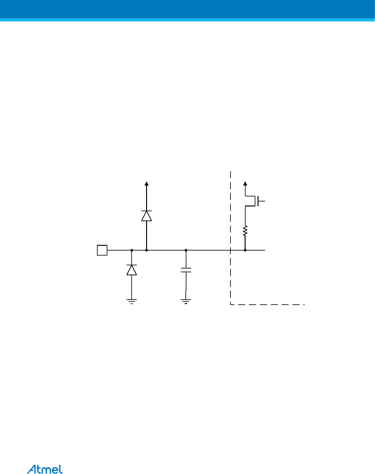
18. I/O Ports
18.1. Overview
All AVR ports have true Read-Modify-Write functionality when used as general digital I/O ports. This
means that the direction of one port pin can be changed without unintentionally changing the direction of
any other pin with the SBI and CBI instructions. The same applies when changing drive value (if
configured as output) or enabling/disabling of pull-up resistors (if configured as input). Each output buffer
has symmetrical drive characteristics with both high sink and source capability. The pin driver is strong
enough to drive LED displays directly. All port pins have individually selectable pull-up resistors with a
supply-voltage invariant resistance. All I/O pins have protection diodes to both VCC and Ground as
indicated in the following figure. Refer to Electrical Characteristics – TA = -40°C to 85°C for a complete
list of parameters.
Figure 18-1 I/O Pin Equivalent Schematic
Cpin
Logic
Rpu
See Figure
"General Digital I/O" for
Details
Pxn
All registers and bit references in this section are written in general form. A lower case “x” represents the
numbering letter for the port, and a lower case “n” represents the bit number. However, when using the
register or bit defines in a program, the precise form must be used (i.e., PORTB3 for bit 3 in Port B, here
documented generally as PORTxn). The physical I/O Registers and bit locations are listed in Register
Description on page 90.
Three I/O memory address locations are allocated for each port, one each for the Data Register –
PORTx, Data Direction Register – DDRx, and the Port Input Pins – PINx. The Port Input Pins I/O location
is read only, while the Data Register and the Data Direction Register are read/write. In addition, the Pull-
up Disable – PUD bit in SFIOR disables the pull-up function for all pins in all ports when set.
Using the I/O port as General Digital I/O is described in Ports as General Digital I/O on page 78. Most
port pins are multiplexed with alternate functions for the peripheral features on the device. How each
alternate function interferes with the port pin is described in Alternate Port Functions on page 81. Refer
to the individual module sections for a full description of the alternate functions.
Note that enabling the alternate function of some of the port pins does not affect the use of the other pins
in the port as general digital I/O.
Related Links
Atmel ATmega8A [DATASHEET]
Atmel-8159F-8-bit AVR Microcontroller_Datasheet_Complete-09/2015
77
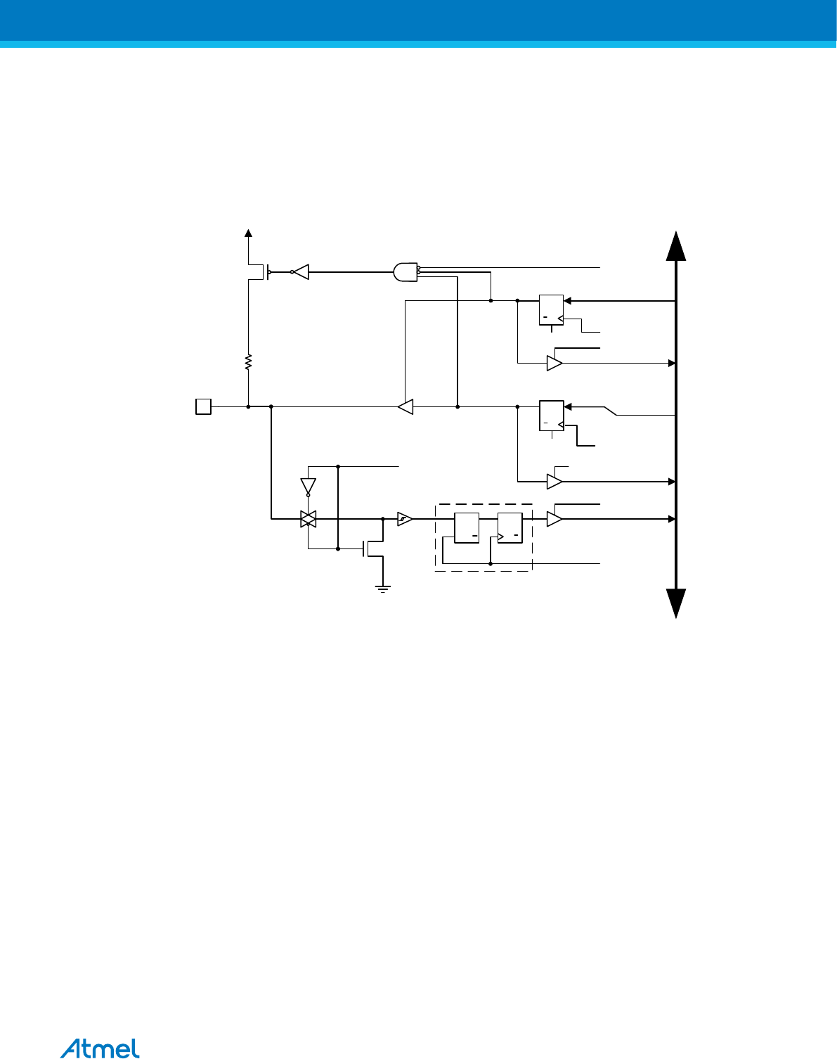
Electrical Characteristics – TA = -40°C to 85°C on page 302
18.2. Ports as General Digital I/O
The ports are bi-directional I/O ports with optional internal pull-ups. The following figure shows a
functional description of one I/O-port pin, here generically called Pxn.
Figure 18-2 General Digital I/O(1)
clk
RPx
RRx
RDx
WDx
PUD
SYNCHRONIZER
WDx: WRITE DDRx
RRx: READ PORTx REGISTER
RPx: READ PORTx PIN
PUD: PULLUP DISABLE
clkI/O: I/O CLOCK
RDx: READ DDRx
D
L
Q
Q
RESET
RESET
Q
QD
Q
Q D
CLR
PORTxn
Q
Q D
CLR
DDxn
PINxn
DATA BUS
SLEEP
SLEEP: SLEEP CONTROL
Pxn
I/O
WPx
WPx: WRITE PINx REGISTER
Note: 1. WPx, WDx, RRx, RPx, and RDx are common to all pins within the same port. clkI/O, SLEEP,
and PUD are common to all ports
18.2.1. Configuring the Pin
Each port pin consists of three register bits: DDxn, PORTxn, and PINxn. As shown in Register
Description on page 90, the DDxn bits are accessed at the DDRx I/O address, the PORTxn bits at the
PORTx I/O address, and the PINxn bits at the PINx I/O address.
The DDxn bit in the DDRx Register selects the direction of this pin. If DDxn is written logic one, Pxn is
configured as an output pin. If DDxn is written logic zero, Pxn is configured as an input pin.
If PORTxn is written logic one when the pin is configured as an input pin, the pull-up resistor is activated.
To switch the pull-up resistor off, PORTxn has to be written logic zero or the pin has to be configured as
an output pin. The port pins are tri-stated when reset condition becomes active, even if no clocks are
running.
If PORTxn is written logic one when the pin is configured as an output pin, the port pin is driven high
(one). If PORTxn is written logic zero when the pin is configured as an output pin, the port pin is driven
low (zero).
When switching between tri-state ({DDxn, PORTxn} = 0b00) and output high ({DDxn, PORTxn} = 0b11),
an intermediate state with either pull-up enabled ({DDxn, PORTxn} = 0b01) or output low ({DDxn,
Atmel ATmega8A [DATASHEET]
Atmel-8159F-8-bit AVR Microcontroller_Datasheet_Complete-09/2015
78
PORTxn} = 0b10) must occur. Normally, the pull-up enabled state is fully acceptable, as a high-impedant
environment will not notice the difference between a strong high driver and a pull-up. If this is not the
case, the PUD bit in the SFIOR Register can be set to disable all pull-ups in all ports.
Switching between input with pull-up and output low generates the same problem. The user must use
either the tristate ({DDxn, PORTxn} = 0b00) or the output high state ({DDxn, PORTxn} = 0b11) as an
intermediate step.
The table below summarizes the control signals for the pin value.
Table 18-1 Port Pin Configurations
DDxn PORTxn PUD (in
SFIOR)
I/O Pull-up Comment
0 0 x Input No Tri-state (Hi-Z)
0 1 0 Input Yes Pxn will source current if
external pulled low.
0 1 1 Input No Tri-state (Hi-Z)
1 0 x Output No Output Low (Sink)
1 1 x Output No Output High (Source)
18.2.2. Reading the Pin Value
Independent of the setting of Data Direction bit DDxn, the port pin can be read through the PINxn
Register Bit. As shown in Figure 18-2 General Digital I/O(1) on page 78, the PINxn Register bit and the
preceding latch constitute a synchronizer. This is needed to avoid metastability if the physical pin changes
value near the edge of the internal clock, but it also introduces a delay. The next figure shows a timing
diagram of the synchronization when reading an externally applied pin value. The maximum and
minimum propagation delays are denoted tpd,max and tpd,min respectively.
Figure 18-3 Synchronization when Reading an Externally Applied Pin value
XXX in r17, PINx
0x00 0xFF
INSTRUCTIONS
SYNC LATCH
PINxn
r17
XXX
SYSTEM CLK
tpd, max
tpd, min
Consider the clock period starting shortly after the first falling edge of the system clock. The latch is
closed when the clock is low, and goes transparent when the clock is high, as indicated by the shaded
region of the “SYNC LATCH” signal. The signal value is latched when the system clock goes low. It is
clocked into the PINxn Register at the succeeding positive clock edge. As indicated by the two arrows
Atmel ATmega8A [DATASHEET]
Atmel-8159F-8-bit AVR Microcontroller_Datasheet_Complete-09/2015
79
tpd,max and tpd,min, a single signal transition on the pin will be delayed between ½ and 1-½ system clock
period depending upon the time of assertion.
When reading back a software assigned pin value, a nop instruction must be inserted as indicated in the
figure below. The out instruction sets the “SYNC LATCH” signal at the positive edge of the clock. In this
case, the delay tpd through the synchronizer is 1 system clock period.
Figure 18-4 Synchronization when Reading a Software Assigned Pin Value
out PORTx, r16 nop in r17, PINx
0xFF
0x00 0xFF
SYSTEM CLK
r16
INSTRUCTIONS
SYNC LATCH
PINxn
r17
tpd
The following code example shows how to set port B pins 0 and 1 high, 2 and 3 low, and define the port
pins from 4 to 7 as input with pull-ups assigned to port pins 6 and 7. The resulting pin values are read
back again, but as previously discussed, a nop instruction is included to be able to read back the value
recently assigned to some of the pins.
Assembly Code Example(1)
:.
; Define pull-ups and set outputs high
; Define directions for port pins
ldi r16,(1<<PB7)|(1<<PB6)|(1<<PB1)|(1<<PB0)
ldi r17,(1<<DDB3)|(1<<DDB2)|(1<<DDB1)|(1<<DDB0)
out PORTB,r16
out DDRB,r17
; Insert nop for synchronization
nop
; Read port pins
in r16,PINB
:.
Atmel ATmega8A [DATASHEET]
Atmel-8159F-8-bit AVR Microcontroller_Datasheet_Complete-09/2015
80

C Code Example(1)
unsigned char i;
:.
/* Define pull-ups and set outputs high */
/* Define directions for port pins */
PORTB = (1<<PB7)|(1<<PB6)|(1<<PB1)|(1<<PB0);
DDRB = (1<<DDB3)|(1<<DDB2)|(1<<DDB1)|(1<<DDB0);
/* Insert nop for synchronization*/
_NOP();
/* Read port pins */
i = PINB;
:.
Note: 1. For the assembly program, two temporary registers are used to minimize the time from pull-ups
are set on pins 0, 1, 6, and 7, until the direction bits are correctly set, defining bit 2 and 3 as low and
redefining bits 0 and 1 as strong high drivers.
18.2.3. Digital Input Enable and Sleep Modes
As shown in figure Figure 18-2 General Digital I/O(1) on page 78, the digital input signal can be clamped
to ground at the input of the Schmitt Trigger. The signal denoted SLEEP in the figure, is set by the MCU
Sleep Controller in Power-down mode, Power-save mode, and Standby mode to avoid high power
consumption if some input signals are left floating, or have an analog signal level close to VCC/2.
SLEEP is overridden for port pins enabled as external interrupt pins. If the external interrupt request is not
enabled, SLEEP is active also for these pins. SLEEP is also overridden by various other alternate
functions as described in Alternate Port Functions on page 81.
If a logic high level (“one”) is present on an Asynchronous External Interrupt pin configured as “Interrupt
on Rising Edge, Falling Edge, or Any Logic Change on Pin” while the external interrupt is not enabled, the
corresponding External Interrupt Flag will be set when resuming from the above mentioned sleep modes,
as the clamping in these sleep modes produces the requested logic change.
18.2.4. Unconnected Pins
If some pins are unused, it is recommended to ensure that these pins have a defined level. Even though
most of the digital inputs are disabled in the deep sleep modes as described above, floating inputs should
be avoided to reduce current consumption in all other modes where the digital inputs are enabled (Reset,
Active mode and Idle mode).
The simplest method to ensure a defined level of an unused pin, is to enable the internal pull-up. In this
case, the pull-up will be disabled during reset. If low power consumption during reset is important, it is
recommended to use an external pull-up or pull-down. Connecting unused pins directly to VCC or GND is
not recommended, since this may cause excessive currents if the pin is accidentally configured as an
output.
18.3. Alternate Port Functions
Most port pins have alternate functions in addition to being general digital I/Os. The following figure
shows how the port pin control signals from the simplified Figure 18-2 General Digital I/O(1) on page 78
can be overridden by alternate functions. The overriding signals may not be present in all port pins, but
the figure serves as a generic description applicable to all port pins in the AVR microcontroller family.
Atmel ATmega8A [DATASHEET]
Atmel-8159F-8-bit AVR Microcontroller_Datasheet_Complete-09/2015
81
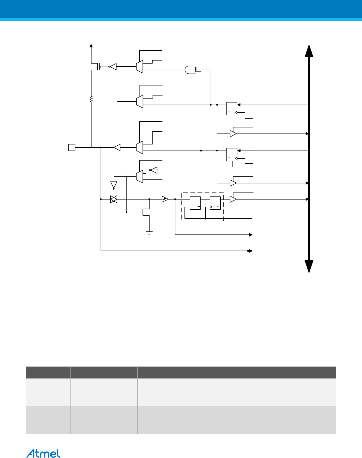
Figure 18-5 Alternate Port Functions(1)
clk
RPx
RRx
RDx
WDx
PUD
SYNCHRONIZER
WDx: WRITE DDRx
RRx: READ PORTx REGISTER
RPx: READ PORTx PIN
PUD: PULLUP DISABLE
clkI/O: I/O CLOCK
RDx: READ DDRx
D
L
Q
Q
SET
CLR
0
1
0
1
0
1
DIxn
AIOxn
DIEOExn
PVOVxn
PVOExn
DDOVxn
DDOExn
PUOExn
PUOVxn
PUOExn: Pxn PULL-UP OVERRIDE ENABLE
PUOVxn: Pxn PULL-UP OVERRIDE VALUE
DDOExn: Pxn DATA DIRECTION OVERRIDE ENABLE
DDOVxn: Pxn DATA DIRECTION OVERRIDE VALUE
PVOExn: Pxn PORT VALUE OVERRIDE ENABLE
PVOVxn: Pxn PORT VALUE OVERRIDE VALUE
DIxn: DIGITAL INPUT PIN n ON PORTx
AIOxn: ANALOG INPUT/OUTPUT PIN n ON PORTx
RESET
RESET
Q
Q D
CLR
Q
Q D
CLR
Q
QD
CLR
PINxn
PORTxn
DDxn
DATA BUS
0
1
DIEOVxn
SLEEP
DIEOExn: Pxn DIGITAL INPUT-ENABLE OVERRIDE ENABLE
DIEOVxn: Pxn DIGITAL INPUT-ENABLE OVERRIDE VALUE
SLEEP: SLEEP CONTROL
Pxn
I/O
WPx: WRITE PINx
WPx
Note: 1. WPx, WDx, RRx, RPx, and RDx are common to all pins within the same port. clkI/O, SLEEP,
and PUD are common to all ports. All other signals are unique for each pin.
The following table summarizes the function of the overriding signals. The pin and port indexes from the
figure above are not shown in the succeeding tables. The overriding signals are generated internally in
the modules having the alternate function.
Table 18-2 Generic Description of Overriding Signals for Alternate Functions
Signal Name Full Name Description
PUOE Pull-up Override
Enable
If this signal is set, the pull-up enable is controlled by the PUOV signal.
If this signal is cleared, the pull-up is enabled when {DDxn, PORTxn,
PUD} = 0b010.
PUOV Pull-up Override Value If PUOE is set, the pull-up is enabled/disabled when PUOV is set/
cleared, regardless of the setting of the DDxn, PORTxn, and PUD
Register bits.
Atmel ATmega8A [DATASHEET]
Atmel-8159F-8-bit AVR Microcontroller_Datasheet_Complete-09/2015
82

Signal Name Full Name Description
DDOE Data Direction
Override Enable
If this signal is set, the Output Driver Enable is controlled by the DDOV
signal. If this signal is cleared, the Output driver is enabled by the DDxn
Register bit.
DDOV Data Direction
Override Value
If DDOE is set, the Output Driver is enabled/disabled when DDOV is
set/cleared, regardless of the setting of the DDxn Register bit.
PVOE Port Value Override
Enable
If this signal is set and the Output Driver is enabled, the port value is
controlled by the PVOV signal. If PVOE is cleared, and the Output
Driver is enabled, the port Value is controlled by the PORTxn Register
bit.
PVOV Port Value Override
Value
If PVOE is set, the port value is set to PVOV, regardless of the setting of
the PORTxn Register bit.
DIEOE Digital Input Enable
Override Enable
If this bit is set, the Digital Input Enable is controlled by the DIEOV
signal. If this signal is cleared, the Digital Input Enable is determined by
MCU state (Normal mode, sleep mode).
DIEOV Digital Input Enable
Override Value
If DIEOE is set, the Digital Input is enabled/disabled when DIEOV is set/
cleared, regardless of the MCU state (Normal mode, sleep mode).
DI Digital Input This is the Digital Input to alternate functions. In the figure, the signal is
connected to the output of the Schmitt Trigger but before the
synchronizer. Unless the Digital Input is used as a clock source, the
module with the alternate function will use its own synchronizer.
AIO Analog Input/Output This is the Analog Input/output to/from alternate functions. The signal is
connected directly to the pad, and can be used bi-directionally.
The following subsections shortly describe the alternate functions for each port, and relate the overriding
signals to the alternate function. Refer to the alternate function description for further details.
18.3.1. Alternate Functions of Port B
The Port B pins with alternate functions are shown in the table below:
Table 18-3 Port B Pins Alternate Functions
Port Pin Alternate Functions
PB7 XTAL2 (Chip Clock Oscillator pin 2)
TOSC2 (Timer Oscillator pin 2)
PB6 XTAL1 (Chip Clock Oscillator pin 1 or External clock input)
TOSC1 (Timer Oscillator pin 1)
PB5 SCK (SPI Bus Master clock Input)
PB4 MISO (SPI Bus Master Input/Slave Output)
PB3 MOSI (SPI Bus Master Output/Slave Input)
OC2 (Timer/Counter2 Output Compare Match Output)
PB2 SS (SPI Bus Master Slave select)
OC1B (Timer/Counter1 Output Compare Match B Output)
Atmel ATmega8A [DATASHEET]
Atmel-8159F-8-bit AVR Microcontroller_Datasheet_Complete-09/2015
83

Port Pin Alternate Functions
PB1 OC1A (Timer/Counter1 Output Compare Match A Output)
PB0 ICP1 (Timer/Counter1 Input Capture Pin)
The alternate pin configuration is as follows:
• XTAL2/TOSC2 – Port B, Bit 7
XTAL2: Chip clock Oscillator pin 2. Used as clock pin for crystal Oscillator or Low-frequency crystal
Oscillator. When used as a clock pin, the pin can not be used as an I/O pin.
TOSC2: Timer Oscillator pin 2. Used only if internal calibrated RC Oscillator is selected as chip clock
source, and the asynchronous timer is enabled by the correct setting in ASSR. When the AS2 bit in ASSR
is set (one) to enable asynchronous clocking of Timer/Counter2, pin PB7 is disconnected from the port,
and becomes the inverting output of the Oscillator amplifier. In this mode, a crystal Oscillator is connected
to this pin, and the pin cannot be used as an I/O pin
If PB7 is used as a clock pin, DDB7, PORTB7 and PINB7 will all read 0.
• XTAL1/TOSC1 – Port B, Bit 6
XTAL1: Chip clock Oscillator pin 1. Used for all chip clock sources except internal calibrated RC
Oscillator. When used as a clock pin, the pin can not be used as an I/O pin.
TOSC1: Timer Oscillator pin 1. Used only if internal calibrated RC Oscillator is selected as chip clock
source, and the asynchronous timer is enabled by the correct setting in ASSR. When the AS2 bit in ASSR
is set (one) to enable asynchronous clocking of Timer/Counter2, pin PB6 is disconnected from the port,
and becomes the input of the inverting Oscillator amplifier. In this mode, a crystal Oscillator is connected
to this pin, and the pin can not be used as an I/O pin.
If PB6 is used as a clock pin, DDB6, PORTB6 and PINB6 will all read 0.
• SCK – Port B, Bit 5
SCK: Master Clock output, Slave Clock input pin for SPI channel. When the SPI is enabled as a Slave,
this pin is configured as an input regardless of the setting of DDB5. When the SPI is enabled as a Master,
the data direction of this pin is controlled by DDB5. When the pin is forced by the SPI to be an input, the
pull-up can still be controlled by the PORTB5 bit.
• MISO – Port B, Bit 4
MISO: Master Data input, Slave Data output pin for SPI channel. When the SPI is enabled as a Master,
this pin is configured as an input regardless of the setting of DDB4. When the SPI is enabled as a Slave,
the data direction of this pin is controlled by DDB4. When the pin is forced by the SPI to be an input, the
pull-up can still be controlled by the PORTB4 bit.
• MOSI/OC2 – Port B, Bit 3
MOSI: SPI Master Data output, Slave Data input for SPI channel. When the SPI is enabled as a Slave,
this pin is configured as an input regardless of the setting of DDB3. When the SPI is enabled as a Master,
the data direction of this pin is controlled by DDB3. When the pin is forced by the SPI to be an input, the
pull-up can still be controlled by the PORTB3 bit.
OC2, Output Compare Match Output: The PB3 pin can serve as an external output for the Timer/
Counter2 Compare Match. The PB3 pin has to be configured as an output (DDB3 set (one)) to serve this
function. The OC2 pin is also the output pin for the PWM mode timer function.
• SS/OC1B – Port B, Bit 2
Atmel ATmega8A [DATASHEET]
Atmel-8159F-8-bit AVR Microcontroller_Datasheet_Complete-09/2015
84
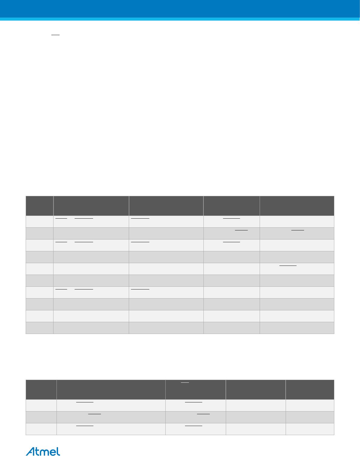
SS: Slave Select input. When the SPI is enabled as a Slave, this pin is configured as an input regardless
of the setting of DDB2. As a Slave, the SPI is activated when this pin is driven low. When the SPI is
enabled as a Master, the data direction of this pin is controlled by DDB2. When the pin is forced by the
SPI to be an input, the pull-up can still be controlled by the PORTB2 bit.
OC1B, Output Compare Match output: The PB2 pin can serve as an external output for the Timer/
Counter1 Compare Match B. The PB2 pin has to be configured as an output (DDB2 set (one)) to serve
this function. The OC1B pin is also the output pin for the PWM mode timer function.
• OC1A – Port B, Bit 1
OC1A, Output Compare Match output: The PB1 pin can serve as an external output for the Timer/
Counter1 Compare Match A. The PB1 pin has to be configured as an output (DDB1 set (one)) to serve
this function. The OC1A pin is also the output pin for the PWM mode timer function.
• ICP1 – Port B, Bit 0
ICP1 – Input Capture Pin: The PB0 pin can act as an Input Capture Pin for Timer/Counter1.
The tables below relate the alternate functions of Port B to the overriding signals shown in figure Figure
18-5 Alternate Port Functions(1) on page 82. SPI MSTR INPUT and SPI SLAVE OUTPUT constitute the
MISO signal, while MOSI is divided into SPI MSTR OUTPUT and SPI SLAVE INPUT.
Table 18-4 Overriding Signals for Alternate Functions in PB7:PB4
Signal
Name
PB7/XTAL2/
TOSC2(1)(2)
PB6/XTAL1/
TOSC1(1)
PB5/SCK PB4/MISO
PUOE EXT • (INTRC + AS2) INTRC + AS2 SPE • MSTR SPE • MSTR
PUO 0 0 PORTB5 • PUD PORTB4 • PUD
DDOE EXT • (INTRC + AS2) INTRC + AS2 SPE • MSTR SPE • MSTR
DDOV 0 0 0 0
PVOE 0 0 SPE • MSTR SPE • MSTR
PVOV 0 0 SCK OUTPUT SPI SLAVE OUTPUT
DIEOE EXT • (INTRC + AS2) INTRC + AS2 0 0
DIEOV 0 0 0 0
DI – – SCK INPUT SPI MSTR INPUT
AIO Oscillator Output Oscillator/Clock Input – –
Note:
1. INTRC means that the internal RC Oscillator is selected (by the CKSEL Fuse).
2. EXT means that the external RC Oscillator or an external clock is selected (by the CKSEL Fuse).
Table 18-5 Overriding Signals for Alternate Functions in PB3:PB0
Signal
Name
PB3/MOSI/
OC2
PB2/SS/
OC1B
PB1/OC1A PB0/ICP1
PUOE SPE • MSTR SPE • MSTR 0 0
PUO PORTB3 • PUD PORTB2 • PUD 0 0
DDOE SPE • MSTR SPE • MSTR 0 0
Atmel ATmega8A [DATASHEET]
Atmel-8159F-8-bit AVR Microcontroller_Datasheet_Complete-09/2015
85
Signal
Name
PB3/MOSI/
OC2
PB2/SS/
OC1B
PB1/OC1A PB0/ICP1
DDOV 0 0 0 0
PVOE SPE • MSTR + OC2 ENABLE OC1B ENABLE OC1A ENABLE 0
PVOV SPI MSTR OUTPUT + OC2 OC1B OC1A 0
DIEOE 0 0 0 0
DIEOV 0 0 0 0
DI SPI SLAVE INPUT SPI SS – ICP1 INPUT
AIO – – – –
18.3.2. Alternate Functions of Port C
The Port C pins with alternate functions are shown in the table below:
Table 18-6 Port C Pins Alternate Functions
Port Pin Alternate Function
PC6 RESET (Reset pin)
PC5 ADC5 (ADC Input Channel 5)
SCL (Two-wire Serial Bus Clock Line)
PC4 ADC4 (ADC Input Channel 4)
SDA (Two-wire Serial Bus Data Input/Output Line)
PC3 ADC3 (ADC Input Channel 3)
PC2 ADC2 (ADC Input Channel 2)
PC1 ADC1 (ADC Input Channel 1)
PC0 ADC0 (ADC Input Channel 0)
The alternate pin configuration is as follows:
• RESET – Port C, Bit 6
RESET, Reset pin: When the RSTDISBL Fuse is programmed, this pin functions as a normal I/O pin, and
the part will have to rely on Power-on Reset and Brown-out Reset as its reset sources. When the
RSTDISBL Fuse is unprogrammed, the reset circuitry is connected to the pin, and the pin can not be
used as an I/O pin.
If PC6 is used as a reset pin, DDC6, PORTC6 and PINC6 will all read 0.
• SCL/ADC5 – Port C, Bit 5
SCL, Two-wire Serial Interface Clock: When the TWEN bit in TWCR is set (one) to enable the Two-wire
Serial Interface, pin PC5 is disconnected from the port and becomes the Serial Clock I/O pin for the Two-
wire Serial Interface. In this mode, there is a spike filter on the pin to suppress spikes shorter than 50 ns
on the input signal, and the pin is driven by an open drain driver with slew-rate limitation.
PC5 can also be used as ADC input Channel 5. Note that ADC input channel 5 uses digital power.
• SDA/ADC4 – Port C, Bit 4
Atmel ATmega8A [DATASHEET]
Atmel-8159F-8-bit AVR Microcontroller_Datasheet_Complete-09/2015
86
SDA, Two-wire Serial Interface Data: When the TWEN bit in TWCR is set (one) to enable the Two-wire
Serial Interface, pin PC4 is disconnected from the port and becomes the Serial Data I/O pin for the Two-
wire Serial Interface. In this mode, there is a spike filter on the pin to suppress spikes shorter than 50 ns
on the input signal, and the pin is driven by an open drain driver with slew-rate limitation.
PC4 can also be used as ADC input Channel 4. Note that ADC input channel 4 uses digital power.
• ADC3 – Port C, Bit 3
PC3 can also be used as ADC input Channel 3. Note that ADC input channel 3 uses analog power.
• ADC2 – Port C, Bit 2
PC2 can also be used as ADC input Channel 2. Note that ADC input channel 2 uses analog power.
• ADC1 – Port C, Bit 1
PC1 can also be used as ADC input Channel 1. Note that ADC input channel 1 uses analog power.
• ADC0 – Port C, Bit 0
PC0 can also be used as ADC input Channel 0. Note that ADC input channel 0 uses analog power.
The tables below relate the alternate functions of Port C to the overriding signals shown in figure Figure
18-5 Alternate Port Functions(1) on page 82.
Table 18-7 Overriding Signals for Alternate Functions in PC6:PC4
Signal
Name
PC6/RESET PC5/SCL/ADC5 PC4/SDA/ADC4
PUOE RSTDISBL TWEN TWEN
PUOV 1 PORTC5 • PUD PORTC4 • PUD
DDOE RSTDISBL TWEN TWEN
DDOV 0 SCL_OUT SDA_OUT
PVOE 0 TWEN TWEN
PVOV 0 0 0
DIEOE RSTDISBL 0 0
DIEOV 0 0 0
DI – – –
AIO RESET INPUT ADC5 INPUT / SCL INPUT ADC4 INPUT / SDA INPUT
Table 18-8 Overriding Signals for Alternate Functions in PC3:PC0(1)
Signal
Name
PC3/A11 PC2/A10 PC1/A9 PC0/A8
PUOE 0 0 0 0
PUOV 0 0 0 0
DDOE 0 0 0 0
DDOV 0 0 0 0
PVOE 0 0 0 0
Atmel ATmega8A [DATASHEET]
Atmel-8159F-8-bit AVR Microcontroller_Datasheet_Complete-09/2015
87
Signal
Name
PC3/A11 PC2/A10 PC1/A9 PC0/A8
PVOV 0 0 0 0
DIEOE 0 0 0 0
DIEOV 0 0 0 0
DI – – – –
AIO ADC3 INPUT ADC2 INPUT ADC1 INPUT ADC0 INPUT
Note: 1. When enabled, the Two-wire Serial Interface enables slew-rate controls on the output pins PC4
and PC5. This is not shown in the figure. In addition, spike filters are connected between the AIO outputs
shown in the port figure and the digital logic of the TWI module.
18.3.3. Alternate Functions of Port D
The Port D pins with alternate functions are shown in the table below:
Table 18-9 Port D Pins Alternate Functions
Port Pin Alternate Function
PD7 AIN1 (Analog Comparator Negative Input)
PD6 AIN0 (Analog Comparator Positive Input)
PD5 T1 (Timer/Counter 1 External Counter Input)
PD4 XCK (USART External Clock Input/Output)
T0 (Timer/Counter 0 External Counter Input)
PD3 INT1 (External Interrupt 1 Input)
PD2 INT0 (External Interrupt 0 Input)
PD1 TXD (USART Output Pin)
PD0 RXD (USART Input Pin)
The alternate pin configuration is as follows:
• AIN1 – Port D, Bit 7
AIN1, Analog Comparator Negative Input. Configure the port pin as input with the internal pull-up
switched off to avoid the digital port function from interfering with the function of the Analog Comparator.
• AIN0 – Port D, Bit 6
AIN0, Analog Comparator Positive Input. Configure the port pin as input with the internal pull-up switched
off to avoid the digital port function from interfering with the function of the Analog Comparator.
• T1 – Port D, Bit 5
T1, Timer/Counter1 counter source.
• XCK/T0 – Port D, Bit 4
XCK, USART external clock.
T0, Timer/Counter0 counter source.
Atmel ATmega8A [DATASHEET]
Atmel-8159F-8-bit AVR Microcontroller_Datasheet_Complete-09/2015
88
• INT1 – Port D, Bit 3
INT1, External Interrupt source 1: The PD3 pin can serve as an external interrupt source.
• INT0 – Port D, Bit 2
INT0, External Interrupt source 0: The PD2 pin can serve as an external interrupt source.
• TXD – Port D, Bit 1
TXD, Transmit Data (Data output pin for the USART). When the USART Transmitter is enabled, this pin is
configured as an output regardless of the value of DDD1.
• RXD – Port D, Bit 0
RXD, Receive Data (Data input pin for the USART). When the USART Receiver is enabled this pin is
configured as an input regardless of the value of DDD0. When the USART forces this pin to be an input,
the pull-up can still be controlled by the PORTD0 bit.
The tables below relate the alternate functions of Port D to the overriding signals shown in figure Figure
18-5 Alternate Port Functions(1) on page 82.
Table 18-10 Overriding Signals for Alternate Functions PD7:PD4
Signal
Name
PD7/AIN1 PD6/AIN0 PD5/T1 PD4/XCK/
T0
PUOE 0 0 0 0
PUO 0 0 0 0
OOE 0 0 0 0
OO 0 0 0 0
PVOE 0 0 0 UMSEL
PVO 0 0 0 XCK OUTPUT
DIEOE 0 0 0 0
DIEO 0 0 0 0
DI – – T1 INPUT XCK INPUT / T0 INPUT
AIO AIN1 INPUT AIN0 INPUT – –
Table 18-11 Overriding Signals for Alternate Functions in PD3:PD0
Signal
Name
PD3/INT1 PD2/INT0 PD1/TXD PD0/RXD
PUOE 0 0 TXEN RXEN
PUO 0 0 0 PORTD0 • PUD
OOE 0 0 TXEN RXEN
OO 0 0 1 0
PVOE 0 0 TXEN 0
PVO 0 0 TXD 0
Atmel ATmega8A [DATASHEET]
Atmel-8159F-8-bit AVR Microcontroller_Datasheet_Complete-09/2015
89

Signal
Name
PD3/INT1 PD2/INT0 PD1/TXD PD0/RXD
DIEOE INT1 ENABLE INT0 ENABLE 0 0
DIEO 1 1 0 0
DI
INT1 INPUT
INT0 INPUT – RXD
AIO – – – –
18.4. Register Description
Atmel ATmega8A [DATASHEET]
Atmel-8159F-8-bit AVR Microcontroller_Datasheet_Complete-09/2015
90

18.4.1. SFIOR – Special Function IO Register
When using the I/O specific commands IN and OUT, the I/O addresses 0x00 - 0x3F must be used. When
addressing I/O Registers as data space using LD and ST instructions, 0x20 must be added to these offset
addresses. The device is a complex microcontroller with more peripheral units than can be supported
within the 64 location reserved in Opcode for the IN and OUT instructions. For the Extended I/O space
from 0x60 in SRAM, only the ST/STS/STD and LD/LDS/LDD instructions can be used.
Name: SFIOR
Offset: 0x30
Reset: 0
Property:
When addressing I/O Registers as data space the offset address is 0x50
Bit 7 6 5 4 3 2 1 0
PUD
Access R/W
Reset 0
Bit 2 – PUD: Pull-up Disable
When this bit is written to one, the pull-ups in the I/O ports are disabled even if the DDxn and PORTxn
Registers are configured to enable the pull-ups ({DDxn, PORTxn} = 0b01). See Configuring the Pin for
more details about this feature.
Atmel ATmega8A [DATASHEET]
Atmel-8159F-8-bit AVR Microcontroller_Datasheet_Complete-09/2015
91

18.4.2. PORTB – The Port B Data Register
When using the I/O specific commands IN and OUT, the I/O addresses 0x00 - 0x3F must be used. When
addressing I/O Registers as data space using LD and ST instructions, 0x20 must be added to these offset
addresses. The device is a complex microcontroller with more peripheral units than can be supported
within the 64 location reserved in Opcode for the IN and OUT instructions. For the Extended I/O space
from 0x60 in SRAM, only the ST/STS/STD and LD/LDS/LDD instructions can be used.
Name: PORTB
Offset: 0x18
Reset: 0x00
Property:
When addressing I/O Registers as data space the offset address is 0x38
Bit 7 6 5 4 3 2 1 0
PORTB7 PORTB6 PORTB5 PORTB4 PORTB3 PORTB2 PORTB1 PORTB0
Access R/W R/W R/W R/W R/W R/W R/W R/W
Reset 0 0 0 0 0 0 0 0
Bits 7:0 – PORTBn: Port B Data [n = 7:0]
Atmel ATmega8A [DATASHEET]
Atmel-8159F-8-bit AVR Microcontroller_Datasheet_Complete-09/2015
92

18.4.3. DDRB – The Port B Data Direction Register
When using the I/O specific commands IN and OUT, the I/O addresses 0x00 - 0x3F must be used. When
addressing I/O Registers as data space using LD and ST instructions, 0x20 must be added to these offset
addresses. The device is a complex microcontroller with more peripheral units than can be supported
within the 64 location reserved in Opcode for the IN and OUT instructions. For the Extended I/O space
from 0x60 in SRAM, only the ST/STS/STD and LD/LDS/LDD instructions can be used.
Name: DDRB
Offset: 0x17
Reset: 0x00
Property:
When addressing I/O Registers as data space the offset address is 0x37
Bit 7 6 5 4 3 2 1 0
DDB7 DDB6 DDB5 DDB4 DDB3 DDB2 DDB1 DDB0
Access R/W R/W R/W R/W R/W R/W R/W R/W
Reset 0 0 0 0 0 0 0 0
Bits 7:0 – DDBn: Port B Data Direction [n = 7:0]
Atmel ATmega8A [DATASHEET]
Atmel-8159F-8-bit AVR Microcontroller_Datasheet_Complete-09/2015
93

18.4.4. PINB – The Port B Input Pins Address
When using the I/O specific commands IN and OUT, the I/O addresses 0x00 - 0x3F must be used. When
addressing I/O Registers as data space using LD and ST instructions, 0x20 must be added to these offset
addresses. The device is a complex microcontroller with more peripheral units than can be supported
within the 64 location reserved in Opcode for the IN and OUT instructions. For the Extended I/O space
from 0x60 in SRAM, only the ST/STS/STD and LD/LDS/LDD instructions can be used.
Name: PINB
Offset: 0x16
Reset: N/A
Property:
When addressing I/O Registers as data space the offset address is 0x36
Bit 7 6 5 4 3 2 1 0
PINB7 PINB6 PINB5 PINB4 PINB3 PINB2 PINB1 PINB0
Access R R R R R R R R
Reset x x x x x x x x
Bits 7:0 – PINBn: Port B Input Pins Address [n = 7:0]
Atmel ATmega8A [DATASHEET]
Atmel-8159F-8-bit AVR Microcontroller_Datasheet_Complete-09/2015
94
18.4.5. PORTC – The Port C Data Register
When using the I/O specific commands IN and OUT, the I/O addresses 0x00 - 0x3F must be used. When
addressing I/O Registers as data space using LD and ST instructions, 0x20 must be added to these offset
addresses. The device is a complex microcontroller with more peripheral units than can be supported
within the 64 location reserved in Opcode for the IN and OUT instructions. For the Extended I/O space
from 0x60 in SRAM, only the ST/STS/STD and LD/LDS/LDD instructions can be used.
Name: PORTC
Offset: 0x15
Reset: 0x00
Property:
When addressing I/O Registers as data space the offset address is 0x35
Bit 7 6 5 4 3 2 1 0
PORTC6 PORTC5 PORTC4 PORTC3 PORTC2 PORTC1 PORTC0
Access R/W R/W R/W R/W R/W R/W R/W
Reset 0 0 0 0 0 0 0
Bits 6:0 – PORTCn: Port C Data [n = 6:0]
Atmel ATmega8A [DATASHEET]
Atmel-8159F-8-bit AVR Microcontroller_Datasheet_Complete-09/2015
95

18.4.6. DDRC – The Port C Data Direction Register
When using the I/O specific commands IN and OUT, the I/O addresses 0x00 - 0x3F must be used. When
addressing I/O Registers as data space using LD and ST instructions, 0x20 must be added to these offset
addresses. The device is a complex microcontroller with more peripheral units than can be supported
within the 64 location reserved in Opcode for the IN and OUT instructions. For the Extended I/O space
from 0x60 in SRAM, only the ST/STS/STD and LD/LDS/LDD instructions can be used.
Name: DDRC
Offset: 0x14
Reset: 0x00
Property:
When addressing I/O Registers as data space the offset address is 0x34
Bit 7 6 5 4 3 2 1 0
DDC6 DDC5 DDC4 DDC3 DDC2 DDC1 DDC0
Access R/W R/W R/W R/W R/W R/W R/W
Reset 0 0 0 0 0 0 0
Bits 6:0 – DDCn: Port C Data Direction [n = 6:0]
Atmel ATmega8A [DATASHEET]
Atmel-8159F-8-bit AVR Microcontroller_Datasheet_Complete-09/2015
96

18.4.7. PINC – The Port C Input Pins Address
When using the I/O specific commands IN and OUT, the I/O addresses 0x00 - 0x3F must be used. When
addressing I/O Registers as data space using LD and ST instructions, 0x20 must be added to these offset
addresses. The device is a complex microcontroller with more peripheral units than can be supported
within the 64 location reserved in Opcode for the IN and OUT instructions. For the Extended I/O space
from 0x60 in SRAM, only the ST/STS/STD and LD/LDS/LDD instructions can be used.
Name: PINC
Offset: 0x13
Reset: N/A
Property:
When addressing I/O Registers as data space the offset address is 0x33
Bit 7 6 5 4 3 2 1 0
PINC6 PINC5 PINC4 PINC3 PINC2 PINC1 PINC0
Access R R R R R R R
Reset x x x x x x x
Bits 6:0 – PINCn: Port C Input Pins Address [n = 6:0]
Atmel ATmega8A [DATASHEET]
Atmel-8159F-8-bit AVR Microcontroller_Datasheet_Complete-09/2015
97

18.4.8. PORTD – The Port D Data Register
When using the I/O specific commands IN and OUT, the I/O addresses 0x00 - 0x3F must be used. When
addressing I/O Registers as data space using LD and ST instructions, 0x20 must be added to these offset
addresses. The device is a complex microcontroller with more peripheral units than can be supported
within the 64 location reserved in Opcode for the IN and OUT instructions. For the Extended I/O space
from 0x60 in SRAM, only the ST/STS/STD and LD/LDS/LDD instructions can be used.
Name: PORTD
Offset: 0x12
Reset: 0x00
Property:
When addressing I/O Registers as data space the offset address is 0x32
Bit 7 6 5 4 3 2 1 0
PORTD7 PORTD6 PORTD5 PORTD4 PORTD3 PORTD2 PORTD1 PORTD0
Access R/W R/W R/W R/W R/W R/W R/W R/W
Reset 0 0 0 0 0 0 0 0
Bits 7:0 – PORTDn: Port D Data [n = 7:0]
Atmel ATmega8A [DATASHEET]
Atmel-8159F-8-bit AVR Microcontroller_Datasheet_Complete-09/2015
98

18.4.9. DDRD – The Port D Data Direction Register
When using the I/O specific commands IN and OUT, the I/O addresses 0x00 - 0x3F must be used. When
addressing I/O Registers as data space using LD and ST instructions, 0x20 must be added to these offset
addresses. The device is a complex microcontroller with more peripheral units than can be supported
within the 64 location reserved in Opcode for the IN and OUT instructions. For the Extended I/O space
from 0x60 in SRAM, only the ST/STS/STD and LD/LDS/LDD instructions can be used.
Name: DDRD
Offset: 0x11
Reset: 0x00
Property:
When addressing I/O Registers as data space the offset address is 0x31
Bit 7 6 5 4 3 2 1 0
DDD7 DDD6 DDD5 DDD4 DDD3 DDD2 DDD1 DDD0
Access R/W R/W R/W R/W R/W R/W R/W R/W
Reset 0 0 0 0 0 0 0 0
Bits 7:0 – DDDn: Port D Data Direction [n = 7:0]
Atmel ATmega8A [DATASHEET]
Atmel-8159F-8-bit AVR Microcontroller_Datasheet_Complete-09/2015
99

18.4.10. PIND – The Port D Input Pins Address
When using the I/O specific commands IN and OUT, the I/O addresses 0x00 - 0x3F must be used. When
addressing I/O Registers as data space using LD and ST instructions, 0x20 must be added to these offset
addresses. The device is a complex microcontroller with more peripheral units than can be supported
within the 64 location reserved in Opcode for the IN and OUT instructions. For the Extended I/O space
from 0x60 in SRAM, only the ST/STS/STD and LD/LDS/LDD instructions can be used.
Name: PIND
Offset: 0x10
Reset: N/A
Property:
When addressing I/O Registers as data space the offset address is 0x30
Bit 7 6 5 4 3 2 1 0
PIND7 PIND6 PIND5 PIND4 PIND3 PIND2 PIND1 PIND0
Access R R R R R R R R
Reset x x x x x x x x
Bits 7:0 – PINDn: Port D Input Pins Address [n = 7:0]
Atmel ATmega8A [DATASHEET]
Atmel-8159F-8-bit AVR Microcontroller_Datasheet_Complete-09/2015
100
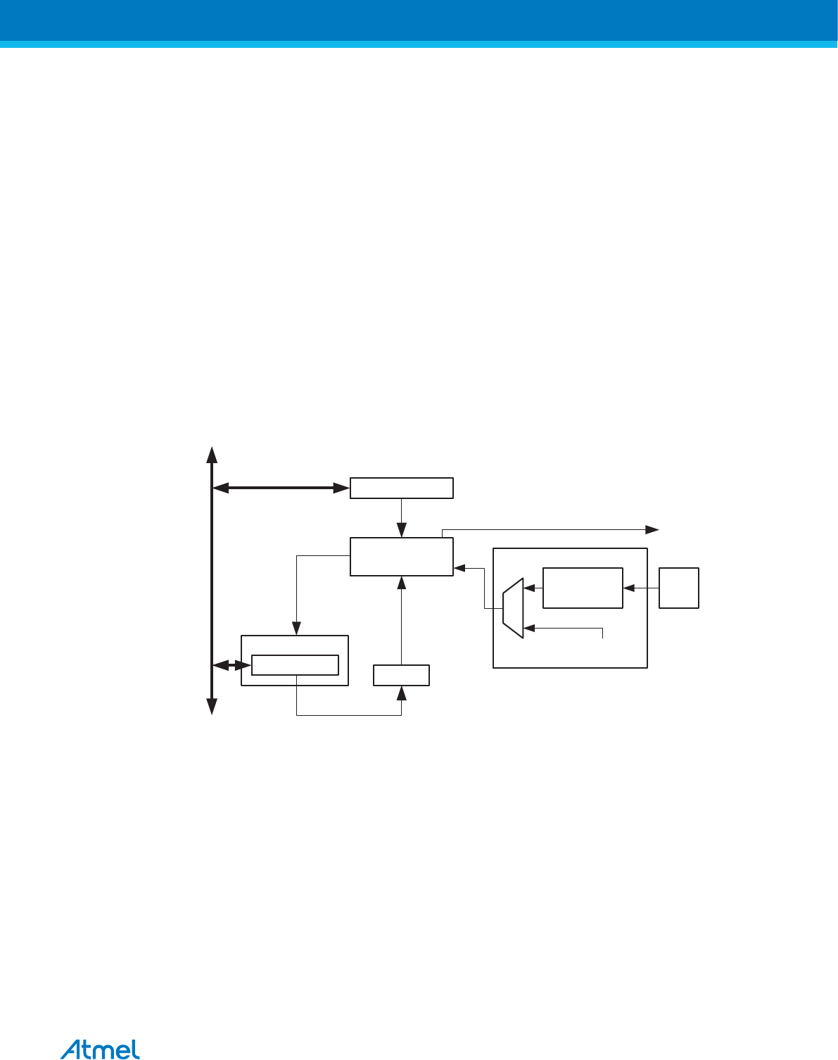
19. 8-bit Timer/Counter0
19.1. Features
• Single Channel Counter
• Frequency Generator
• External Event Counter
• 10-bit Clock Prescaler
19.2. Overview
Timer/Counter0 is a general purpose, single channel, 8-bit Timer/Counter module. A simplified block
diagram of the 8-bit Timer/Counter is shown in the figure below. For the actual placement of I/O pins, refer
to Pin Configurations. CPU accessible I/O Registers, including I/O bits and I/O pins, are shown in bold.
The device-specific I/O Register and bit locations are listed in the Register Description.
Figure 19-1 8-bit Timer/Counter Block Diagram
Timer/Counte r
DATA BUS
TCNTn
Control Logic
= 0xFF
count
TOVn
(Int.Req.)
TCCRn
Clock Se le ct
Tn
Edge
Dete ctor
( From Pre sca ler )
clkTn
Related Links
Pin Configurations on page 13
19.2.1. Registers
The Timer/Counter (TCNT0) is an 8-bit register. Interrupt request (abbreviated to Int. Req. in the figure)
signals are all visible in the Timer Interrupt Flag Register (TIFR). All interrupts are individually masked
with the Timer Interrupt Mask Register (TIMSK). TIFR and TIMSK are not shown in the figure since these
registers are shared by other timer units.
The Timer/Counter can be clocked internally or via the prescaler, or by an external clock source on the T0
pin. The Clock Select logic block controls which clock source and edge the Timer/Counter uses to
increment its value. The Timer/Counter is inactive when no clock source is selected. The output from the
clock select logic is referred to as the timer clock (clkT0).
Atmel ATmega8A [DATASHEET]
Atmel-8159F-8-bit AVR Microcontroller_Datasheet_Complete-09/2015
101
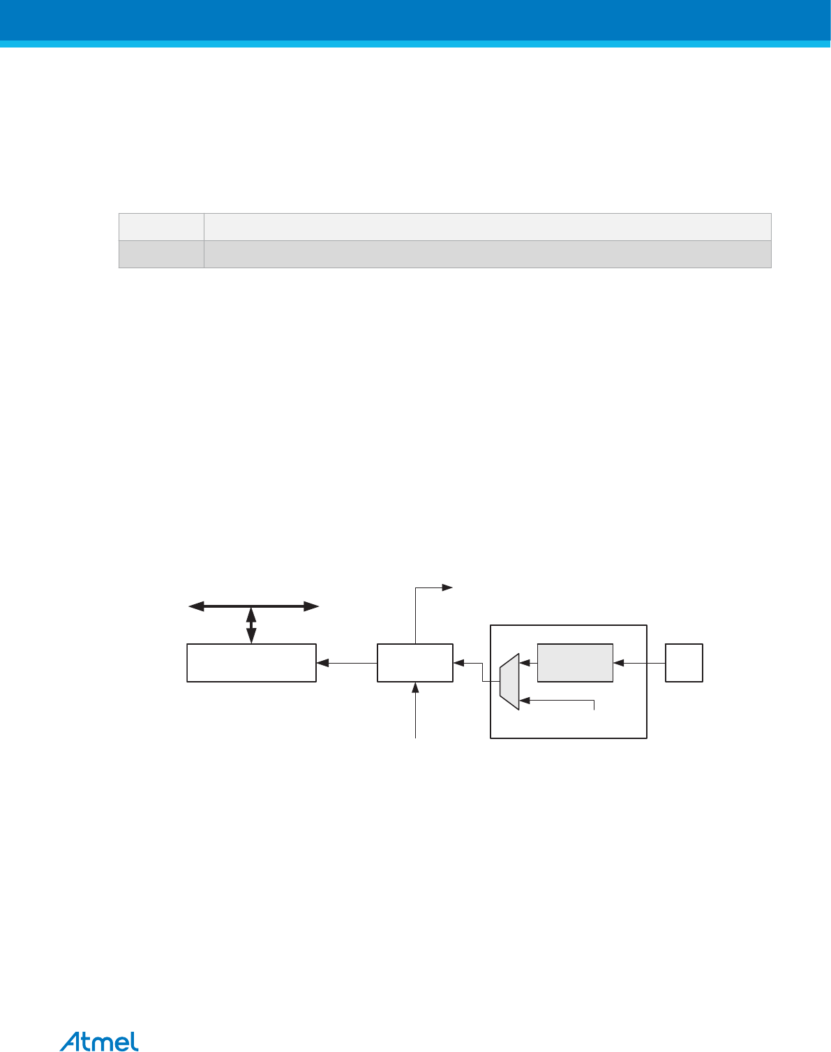
19.2.2. Definitions
Many register and bit references in this document are written in general form. A lower case “n” replaces
the Timer/Counter number, in this case 0. However, when using the register or bit defines in a program,
the precise form must be used i.e. TCNT0 for accessing Timer/Counter0 counter value and so on.
The definitions in the table below are also used extensively throughout this datasheet.
Table 19-1 Definitions
BOTTOM The counter reaches the BOTTOM when it becomes 0x00
MAX The counter reaches its MAXimum when it becomes 0xFF (decimal 255)
19.3. Timer/Counter Clock Sources
The Timer/Counter can be clocked by an internal or an external clock source. The clock source is
selected by the clock select logic which is controlled by the clock select (CS02:0) bits located in the
Timer/Counter Control Register (TCCR0). For details on clock sources and prescaler, see Timer/Counter0
and Timer/Counter1 Prescalers.
Related Links
Timer/Counter0 and Timer/Counter1 Prescalers on page 108
19.4. Counter Unit
The main part of the 8-bit Timer/Counter is the programmable counter unit. The following figure shows a
block diagram of the counter and its surroundings.
Figure 19-2 Counter Unit Block Diagram
DATA BUS
TCNTn Control Logic
count
TOVn
(Int. Re q.)
Clock S e le ct
ma x
Tn
Edge
Dete ctor
( From Pres caler )
clkTn
Signal description (internal signals):
count Increment TCNT0 by 1.
clkTn Timer/Counter clock, referred to as clkT0 in the following.
max Signalize that TCNT0 has reached maximum value.
The counter is incremented at each timer clock (clkT0). clkT0 can be generated from an external or internal
clock source, selected by the clock select bits (CS02:0). When no clock source is selected (CS02:0 = 0)
the timer is stopped. However, the TCNT0 value can be accessed by the CPU, regardless of whether
clkT0 is present or not. A CPU write overrides (has priority over) all counter clear or count operations.
Atmel ATmega8A [DATASHEET]
Atmel-8159F-8-bit AVR Microcontroller_Datasheet_Complete-09/2015
102
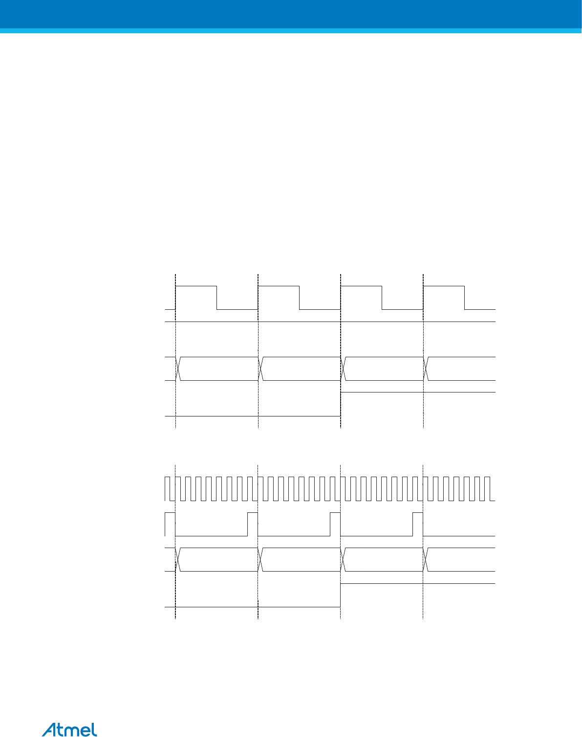
19.5. Operation
The counting direction is always up (incrementing), and no counter clear is performed. The counter simply
overruns when it passes its maximum 8-bit value (MAX = 0xFF) and then restarts from the bottom (0x00).
In normal operation the Timer/Counter Overflow Flag (TOV0) will be set in the same timer clock cycle as
the TCNT0 becomes zero. The TOV0 Flag in this case behaves like a ninth bit, except that it is only set,
not cleared. However, combined with the timer overflow interrupt that automatically clears the TOV0 Flag,
the timer resolution can be increased by software. A new counter value can be written anytime.
19.6. Timer/Counter Timing Diagrams
The Timer/Counter is a synchronous design and the timer clock (clkT0) is therefore shown as a clock
enable signal in the following figures. The figures include information on when Interrupt Flags are set. The
following figure contains timing data for basic Timer/Counter operation. The figure shows the count
sequence close to the MAX value.
Figure 19-3 Timer/Counter Timing Diagram, No Prescaling
clkTn
(clkI/O/1)
TOVn
clkI/O
TCNTn MAX - 1 MAX BOTTOM BOTTOM + 1
The next figure shows the same timing data, but with the prescaler enabled.
Figure 19-4 Timer/Counter Timing Diagram, with Prescaler (fclk_I/O/8)
TOVn
TCNTn MAX - 1 MAX BOTTOM BOTTOM + 1
clkI/O
clkTn
(clkI/O/8)
19.7. Register Description
Atmel ATmega8A [DATASHEET]
Atmel-8159F-8-bit AVR Microcontroller_Datasheet_Complete-09/2015
103
19.7.1. TCCR0 – Timer/Counter Control Register
When using the I/O specific commands IN and OUT, the I/O addresses 0x00 - 0x3F must be used. When
addressing I/O Registers as data space using LD and ST instructions, 0x20 must be added to these offset
addresses. The device is a complex microcontroller with more peripheral units than can be supported
within the 64 location reserved in Opcode for the IN and OUT instructions. For the Extended I/O space
from 0x60 in SRAM, only the ST/STS/STD and LD/LDS/LDD instructions can be used.
Name: TCCR0
Offset: 0x33
Reset: 0
Property:
When addressing I/O Registers as data space the offset address is 0x53
Bit 7 6 5 4 3 2 1 0
CS02 CS01 CS00
Access R/W R/W R/W
Reset 0 0 0
Bits 2:0 – CS0n: Clock Select [n = 2:0]
The three clock select bits select the clock source to be used by the Timer/Counter.
CS02 CS01 CS00 Description
0 0 0 No clock source (Timer/Counter stopped).
0 0 1 clkI/O/(No prescaling)
0 1 0 clkI/O/8 (From prescaler)
0 1 1 clkI/O/64 (From prescaler)
1 0 0 clkI/O/256 (From prescaler)
1 0 1 clkI/O/1024 (From prescaler)
1 1 0 External clock source on T0 pin. Clock on falling edge.
1 1 1 External clock source on T0 pin. Clock on rising edge.
If external pin modes are used for the Timer/Counter0, transitions on the T0 pin will clock the counter
even if the pin is configured as an output. This feature allows software control of the counting.
Atmel ATmega8A [DATASHEET]
Atmel-8159F-8-bit AVR Microcontroller_Datasheet_Complete-09/2015
104

19.7.2. TCNT0 – Timer/Counter Register
When using the I/O specific commands IN and OUT, the I/O addresses 0x00 - 0x3F must be used. When
addressing I/O Registers as data space using LD and ST instructions, 0x20 must be added to these offset
addresses. The device is a complex microcontroller with more peripheral units than can be supported
within the 64 location reserved in Opcode for the IN and OUT instructions. For the Extended I/O space
from 0x60 in SRAM, only the ST/STS/STD and LD/LDS/LDD instructions can be used.
Name: TCNT0
Offset: 0x32
Reset: 0
Property:
When addressing I/O Registers as data space the offset address is 0x52
Bit 7 6 5 4 3 2 1 0
TCNT0[7:0]
Access R/W R/W R/W R/W R/W R/W R/W R/W
Reset 0 0 0 0 0 0 0 0
Bits 7:0 – TCNT0[7:0]
The Timer/Counter Register gives direct access, both for read and write operations, to the Timer/Counter
unit 8-bit counter.
Atmel ATmega8A [DATASHEET]
Atmel-8159F-8-bit AVR Microcontroller_Datasheet_Complete-09/2015
105

19.7.3. TIMSK – Timer/Counter Interrupt Mask Register
When using the I/O specific commands IN and OUT, the I/O addresses 0x00 - 0x3F must be used. When
addressing I/O Registers as data space using LD and ST instructions, 0x20 must be added to these offset
addresses. The device is a complex microcontroller with more peripheral units than can be supported
within the 64 location reserved in Opcode for the IN and OUT instructions. For the Extended I/O space
from 0x60 in SRAM, only the ST/STS/STD and LD/LDS/LDD instructions can be used.
Name: TIMSK
Offset: 0x39
Reset: 0
Property:
When addressing I/O Registers as data space the offset address is 0x59
Bit 7 6 5 4 3 2 1 0
TOIE0
Access R/W
Reset 0
Bit 0 – TOIE0: Timer/Counter0 Overflow Interrupt Enable.
When the TOIE0 bit is written to one, and the I-bit in the Status Register is set (one), the Timer/Counter0
Overflow interrupt is enabled. The corresponding interrupt is executed if an overflow in Timer/Counter0
occurs, i.e., when the TOV0 bit is set in the Timer/Counter Interrupt Flag Register – TIFR.
Atmel ATmega8A [DATASHEET]
Atmel-8159F-8-bit AVR Microcontroller_Datasheet_Complete-09/2015
106

19.7.4. TIFR – Timer/Counter Interrupt Flag Register
When using the I/O specific commands IN and OUT, the I/O addresses 0x00 - 0x3F must be used. When
addressing I/O Registers as data space using LD and ST instructions, 0x20 must be added to these offset
addresses. The device is a complex microcontroller with more peripheral units than can be supported
within the 64 location reserved in Opcode for the IN and OUT instructions. For the Extended I/O space
from 0x60 in SRAM, only the ST/STS/STD and LD/LDS/LDD instructions can be used.
Name: TIFR
Offset: 0x38
Reset: 0
Property:
When addressing I/O Registers as data space the offset address is 0x58
Bit 7 6 5 4 3 2 1 0
TOV0
Access R/W
Reset 0
Bit 0 – TOV0: Timer/Counter0 Overflow Flag
The bit TOV0 is set (one) when an overflow occurs in Timer/Counter0. TOV0 is cleared by hardware
when executing the corresponding interrupt Handling Vector. Alternatively, TOV0 is cleared by writing a
logic one to the flag. When the SREG I-bit, TOIE0 (Timer/Counter0 Overflow Interrupt Enable), and TOV0
are set (one), the Timer/Counter0 Overflow interrupt is executed.
Atmel ATmega8A [DATASHEET]
Atmel-8159F-8-bit AVR Microcontroller_Datasheet_Complete-09/2015
107

20. Timer/Counter0 and Timer/Counter1 Prescalers
20.1. Overview
Timer/Counter1 and Timer/Counter0 share the same prescaler module, but the Timer/Counters can have
different prescaler settings. The description below applies to Timer/Counter1 and Timer/Counter0.
20.2. Internal Clock Source
The Timer/Counter can be clocked directly by the system clock (by setting the CSn2:0 = 1). This provides
the fastest operation, with a maximum Timer/Counter clock frequency equal to system clock frequency
(fCLK_I/O). Alternatively, one of four taps from the prescaler can be used as a clock source. The prescaled
clock has a frequency of either fCLK_I/O/8, fCLK_I/O/64, fCLK_I/O/256, or fCLK_I/O/1024.
20.3. Prescaler Reset
The prescaler is free running (i.e., operates independently of the clock select logic of the Timer/Counter)
and it is shared by Timer/Counter1 and Timer/Counter0. Since the prescaler is not affected by the Timer/
Counter’s clock select, the state of the prescaler will have implications for situations where a prescaled
clock is used. One example of prescaling artifacts occurs when the timer is enabled and clocked by the
prescaler (6 > CSn2:0 > 1). The number of system clock cycles from when the timer is enabled to the first
count occurs can be from 1 to N+1 system clock cycles, where N equals the prescaler divisor (8, 64, 256,
or 1024).
It is possible to use the prescaler reset for synchronizing the Timer/Counter to program execution.
However, care must be taken if the other Timer/Counter that shares the same prescaler also uses
prescaling. A prescaler reset will affect the prescaler period for all Timer/Counters it is connected to.
20.4. External Clock Source
An external clock source applied to the T1/T0 pin can be used as Timer/Counter clock (clkT1/clkT0). The
T1/T0 pin is sampled once every system clock cycle by the pin synchronization logic. The synchronized
(sampled) signal is then passed through the edge detector. The figure below shows a functional
equivalent block diagram of the T1/T0 synchronization and edge detector logic. The registers are clocked
at the positive edge of the internal system clock (clkI/O). The latch is transparent in the high period of the
internal system clock.
The edge detector generates one clkT1/clkT0 pulse for each positive (CSn2:0 = 7) or negative (CSn2:0 =
6) edge it detects.
Figure 20-1 T1/T0 Pin Sampling
Tn_s ync
(To Clock
Select Logic)
Edge De te ctorSynchronization
D QD Q
LE
D Q
Tn
clkI/O
Atmel ATmega8A [DATASHEET]
Atmel-8159F-8-bit AVR Microcontroller_Datasheet_Complete-09/2015
108
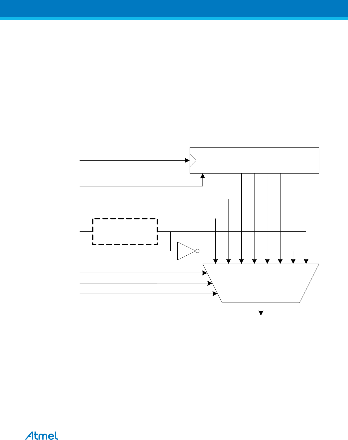
The synchronization and edge detector logic introduces a delay of 2.5 to 3.5 system clock cycles from an
edge has been applied to the T1/T0 pin to the counter is updated.
Enabling and disabling of the clock input must be done when T1/T0 has been stable for at least one
system clock cycle, otherwise it is a risk that a false Timer/Counter clock pulse is generated.
Each half period of the external clock applied must be longer than one system clock cycle to ensure
correct sampling. The external clock must be guaranteed to have less than half the system clock
frequency (fExtClk < fclk_I/O/2) given a 50/50% duty cycle. Since the edge detector uses sampling, the
maximum frequency of an external clock it can detect is half the sampling frequency (Nyquist sampling
theorem). However, due to variation of the system clock frequency and duty cycle caused by Oscillator
source (crystal, resonator, and capacitors) tolerances, it is recommended that maximum frequency of an
external clock source is less than fclk_I/O/2.5.
An external clock source can not be prescaled.
Figure 20-2 Prescaler for Timer/Counter1 and Timer/Counter0(1)
CSn0
CSn1
CSn2
Synchronization
10-BIT T/C PRESCALER
Tn
clkI/O
PSR10
Clear
CK/8
CK/256
CK/64
CK/1024
OFF
TIMER/COUNTERn CLOCK
SOURCE clk Tn
Note: 1. The synchronization logic on the input pins (T1/T0) is shown in figure T1/T0 Pin Sampling in
this section.
20.5. Register Description
Atmel ATmega8A [DATASHEET]
Atmel-8159F-8-bit AVR Microcontroller_Datasheet_Complete-09/2015
109

20.5.1. SFIOR – Special Function IO Register
When using the I/O specific commands IN and OUT, the I/O addresses 0x00 - 0x3F must be used. When
addressing I/O Registers as data space using LD and ST instructions, 0x20 must be added to these offset
addresses. The device is a complex microcontroller with more peripheral units than can be supported
within the 64 location reserved in Opcode for the IN and OUT instructions. For the Extended I/O space
from 0x60 in SRAM, only the ST/STS/STD and LD/LDS/LDD instructions can be used.
Name: SFIOR
Offset: 0x30
Reset: 0
Property:
When addressing I/O Registers as data space the offset address is 0x50
Bit 7 6 5 4 3 2 1 0
PSR10
Access R/W
Reset 0
Bit 0 – PSR10: Prescaler Reset Timer/Counter1 and Timer/Counter0
When this bit is written to one, the Timer/Counter1 and Timer/Counter0 prescaler will be reset. The bit will
be cleared by hardware after the operation is performed. Writing a zero to this bit will have no effect. Note
that Timer/Counter1 and Timer/Counter0 share the same prescaler and a reset of this prescaler will affect
both timers. This bit will always be read as zero.
Atmel ATmega8A [DATASHEET]
Atmel-8159F-8-bit AVR Microcontroller_Datasheet_Complete-09/2015
110

21. 16-bit Timer/Counter1
21.1. Features
•True 16-bit Design (i.e., allows 16-bit PWM)
•Two independent Output Compare Units
•Double Buffered Output Compare Registers
•One Input Capture Unit
•Input Capture Noise Canceler
•Clear Timer on Compare Match (Auto Reload)
•Glitch-free, Phase Correct Pulse Width Modulator (PWM)
•Variable PWM Period
•Frequency Generator
•External Event Counter
•Four independent interrupt Sources (TOV1, OCF1A, OCF1B, and ICF1)
21.2. Overview
The 16-bit Timer/Counter unit allows accurate program execution timing (event management), wave
generation, and signal timing measurement. Most register and bit references in this section are written in
general form. A lower case “n” replaces the Timer/Counter number, and a lower case “x” replaces the
Output Compare unit channel. However, when using the register or bit defines in a program, the precise
form must be used i.e., TCNT1 for accessing Timer/Counter1 counter value and so on.
A simplified block diagram of the 16-bit Timer/Counter is shown in the following figure. For the actual
placement of I/O pins, refer to Pin Configurations. CPU accessible I/O Registers, including I/O bits and
I/O pins, are shown in bold. The device-specific I/O Register and bit locations are listed in the Register
Description.
Atmel ATmega8A [DATASHEET]
Atmel-8159F-8-bit AVR Microcontroller_Datasheet_Complete-09/2015
111
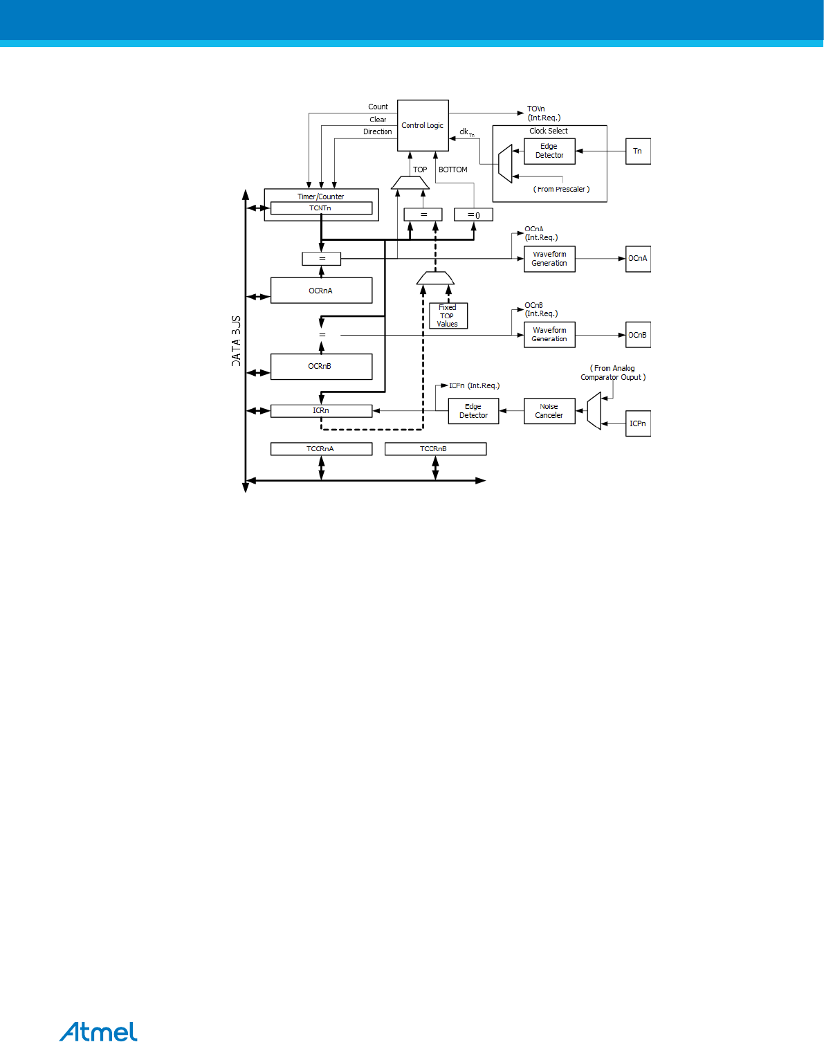
Figure 21-1 16-bit Timer/Counter Block Diagram(1)
Note: 1. Refer to Pin Configurations, table Port B Pins Alternate Functions in Alternate Functions of Port
B, and table Port D Pins Alternate Functions in Alternate Functions of Port D for Timer/Counter1 pin
placement and description.
Related Links
Pin Configurations on page 13
Alternate Functions of Port B on page 83
Alternate Functions of Port D on page 88
21.2.1. Registers
The Timer/Counter (TCNT1), Output Compare Registers (OCR1A/B), and Input Capture Register (ICR1)
are all 16-bit registers. Special procedures must be followed when accessing the 16-bit registers. These
procedures are described in the section Accessing 16-bit Registers on page 17. The Timer/Counter
Control Registers (TCCR1A/B) are 8-bit registers and have no CPU access restrictions. Interrupt requests
(abbreviated to Int.Req. in the figure) signals are all visible in the Timer Interrupt Flag Register (TIFR). All
interrupts are individually masked with the Timer Interrupt Mask Register (TIMSK). TIFR and TIMSK are
not shown in the figure since these registers are shared by other timer units.
The Timer/Counter can be clocked internally, via the prescaler, or by an external clock source on the T1
pin. The Clock Select logic block controls which clock source and edge the Timer/Counter uses to
increment (or decrement) its value. The Timer/Counter is inactive when no clock source is selected. The
output from the clock select logic is referred to as the timer clock (clkT1).
The double buffered Output Compare Registers (OCR1A/B) are compared with the Timer/Counter value
at all time. The result of the compare can be used by the waveform generator to generate a PWM or
variable frequency output on the Output Compare Pin (OC1A/B). See Output Compare Units on page
119. The Compare Match event will also set the Compare Match Flag (OCF1A/B) which can be used to
generate an Output Compare interrupt request.
Atmel ATmega8A [DATASHEET]
Atmel-8159F-8-bit AVR Microcontroller_Datasheet_Complete-09/2015
112

The Input Capture Register can capture the Timer/Counter value at a given external (edge triggered)
event on either the Input Capture Pin (ICP1) or on the Analog Comparator pins (see Analog Comparator).
The Input Capture unit includes a digital filtering unit (Noise Canceler) for reducing the chance of
capturing noise spikes.
The TOP value, or maximum Timer/Counter value, can in some modes of operation be defined by either
the OCR1A Register, the ICR1 Register, or by a set of fixed values. When using OCR1A as TOP value in
a PWM mode, the OCR1A Register can not be used for generating a PWM output. However, the TOP
value will in this case be double buffered allowing the TOP value to be changed in run time. If a fixed TOP
value is required, the ICR1 Register can be used as an alternative, freeing the OCR1A to be used as
PWM output.
Related Links
Analog Comparator on page 243
21.2.2. Definitions
The following definitions are used extensively throughout the document:
Table 21-1 Definitions
BOTTOM The counter reaches the BOTTOM when it becomes 0x0000.
MAX The counter reaches its MAXimum when it becomes 0xFFFF (decimal 65535).
TOP The counter reaches the TOP when it becomes equal to the highest value in the count
sequence. The TOP value can be assigned to be one of the fixed values: 0x00FF, 0x01FF, or
0x03FF, or to the value stored in the OCR1A or ICR1 Register. The assignment is dependent
of the mode of operation.
21.2.3. Compatibility
The 16-bit Timer/Counter has been updated and improved from previous versions of the 16-bit AVR
Timer/Counter. This 16-bit Timer/Counter is fully compatible with the earlier version regarding:
•All 16-bit Timer/Counter related I/O Register address locations, including Timer Interrupt Registers.
•Bit locations inside all 16-bit Timer/Counter Registers, including Timer Interrupt Registers.
•Interrupt Vectors.
The following control bits have changed name, but have same functionality and register location:
•PWM10 is changed to WGM10.
•PWM11 is changed to WGM11.
•CTC1 is changed to WGM12.
The following bits are added to the 16-bit Timer/Counter Control Registers:
•FOC1A and FOC1B are added to TCCR1A.
•WGM13 is added to TCCR1B.
The 16-bit Timer/Counter has improvements that will affect the compatibility in some special cases.
21.3. Accessing 16-bit Registers
The TCNT1, OCR1A/B, and ICR1 are 16-bit registers that can be accessed by the AVR CPU via the 8-bit
data bus. A 16-bit register must be byte accessed using two read or write operations. The 16-bit timer has
a single 8-bit register for temporary storing of the High byte of the 16-bit access. The same temporary
register is shared between all 16-bit registers within the 16-bit timer. Accessing the Low byte triggers the
Atmel ATmega8A [DATASHEET]
Atmel-8159F-8-bit AVR Microcontroller_Datasheet_Complete-09/2015
113

16-bit read or write operation. When the Low byte of a 16-bit register is written by the CPU, the High byte
stored in the temporary register, and the Low byte written are both copied into the 16-bit register in the
same clock cycle. When the Low byte of a 16-bit register is read by the CPU, the High byte of the 16-bit
register is copied into the temporary register in the same clock cycle as the Low byte is read.
Not all 16-bit accesses uses the temporary register for the High byte. Reading the OCR1A/B 16-bit
registers does not involve using the temporary register.
To do a 16-bit write, the High byte must be written before the Low byte. For a 16-bit read, the Low byte
must be read before the High byte.
The following code examples show how to access the 16-bit Timer Registers assuming that no interrupts
updates the temporary register. The same principle can be used directly for accessing the OCR1A/B and
ICR1 Registers. Note that when using “C”, the compiler handles the 16-bit access.
Assembly Code Example(1)
:.
; Set TCNT1 to 0x01FF
ldi r17,0x01
ldi r16,0xFF
out TCNT1H,r17
out TCNT1L,r16
; Read TCNT1 into r17:r16
in r16,TCNT1L
in r17,TCNT1H
:.
C Code Example(1)
unsigned int i;
:.
/* Set TCNT1 to 0x01FF */
TCNT1 = 0x1FF;
/* Read TCNT1 into i */
i = TCNT1;
:.
Note: 1. See About Code Examples.
The assembly code example returns the TCNT1 value in the r17:r16 Register pair.
It is important to notice that accessing 16-bit registers are atomic operations. If an interrupt occurs
between the two instructions accessing the 16-bit register, and the interrupt code updates the temporary
register by accessing the same or any other of the 16-bit Timer Registers, then the result of the access
outside the interrupt will be corrupted. Therefore, when both the main code and the interrupt code update
the temporary register, the main code must disable the interrupts during the 16-bit access.
The following code examples show how to do an atomic read of the TCNT1 Register contents. Reading
any of the OCR1A/B or ICR1 Registers can be done by using the same principle.
Asesmbly Code Example(1)
TIM16_ReadTCNT1:
; Save global interrupt flag
in r18,SREG
; Disable interrupts
cli
Atmel ATmega8A [DATASHEET]
Atmel-8159F-8-bit AVR Microcontroller_Datasheet_Complete-09/2015
114

; Read TCNT1 into r17:r16
in r16,TCNT1L
in r17,TCNT1H
; Restore global interrupt flag
out SREG,r18
ret
C Code Example(1)
unsigned int TIM16_ReadTCNT1( void )
{
unsigned char sreg;
unsigned int i;
/* Save global interrupt flag */
sreg = SREG;
/* Disable interrupts */
_CLI();
/* Read TCNT1 into i */
i = TCNT1;
/* Restore global interrupt flag */
SREG = sreg;
return i;
}
Note: 1. See About Code Examples.
The assembly code example returns the TCNT1 value in the r17:r16 Register pair.
The following code examples show how to do an atomic write of the TCNT1 Register contents. Writing
any of the OCR1A/B or ICR1 Registers can be done by using the same principle.
Assembly Code Example(1)
TIM16_WriteTCNT1:
; Save global interrupt flag
in r18,SREG
; Disable interrupts
cli
; Set TCNT1 to r17:r16
out TCNT1H,r17
out TCNT1L,r16
; Restore global interrupt flag
out SREG,r18
ret
C Code Example(1)
void TIM16_WriteTCNT1( unsigned int i )
{
unsigned char sreg;
unsigned int i;
/* Save global interrupt flag */
sreg = SREG;
/* Disable interrupts */
_CLI();
/* Set TCNT1 to i */
TCNT1 = i;
/* Restore global interrupt flag */
Atmel ATmega8A [DATASHEET]
Atmel-8159F-8-bit AVR Microcontroller_Datasheet_Complete-09/2015
115
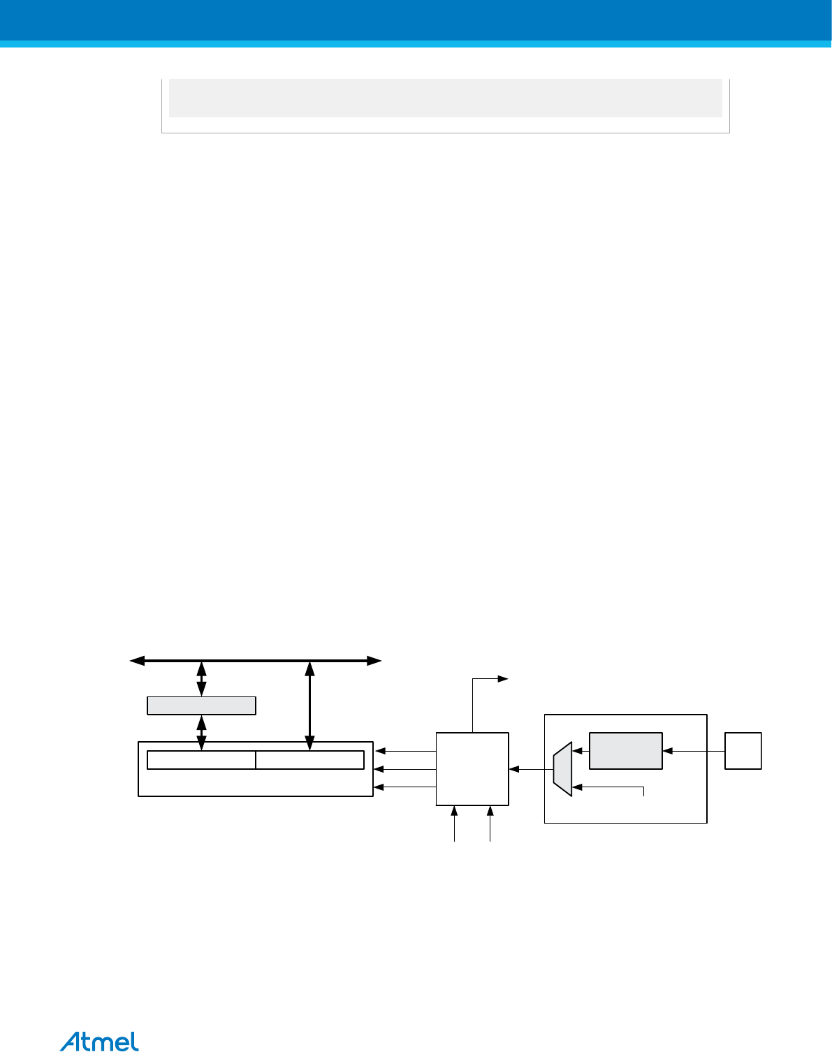
SREG = sreg;
}
Note: 1. See About Code Examples.
The assembly code example requires that the r17:r16 Register pair contains the value to be written to
TCNT1.
Related Links
About Code Examples on page 23
21.3.1. Reusing the Temporary High Byte Register
If writing to more than one 16-bit register where the High byte is the same for all registers written, then the
High byte only needs to be written once. However, note that the same rule of atomic operation described
previously also applies in this case.
21.4. Timer/Counter Clock Sources
The Timer/Counter can be clocked by an internal or an external clock source. The clock source is
selected by the clock select logic which is controlled by the clock select (CS12:0) bits located in the
Timer/Counter Control Register B (TCCR1B). For details on clock sources and prescaler, see Timer/
Counter1 and Timer/Counter0 Prescalers.
Related Links
Timer/Counter0 and Timer/Counter1 Prescalers on page 108
21.5. Counter Unit
The main part of the 16-bit Timer/Counter is the programmable 16-bit bi-directional counter unit. The
figure below shows a block diagram of the counter and its surroundings.
Figure 21-2 Counter Unit Block Diagram
TEMP (8-bit)
DATA BUS (8-bit)
TCNTn (16-bit Counter)
TCNTnH (8-bit) TCNTnL (8-bit) Control Logic
Count
Clear
Direction
TOVn
(Int.Req.)
Clock Select
TOP BOTTOM
Tn
Edge
Detector
( From Prescaler )
clkTn
Signal description (internal signals):
count Increment or decrement TCNT1 by 1.
direction Select between increment and decrement.
clear Clear TCNT1 (set all bits to zero).
clkT1 Timer/Counter clock.
TOP Signalize that TCNT1 has reached maximum value.
Atmel ATmega8A [DATASHEET]
Atmel-8159F-8-bit AVR Microcontroller_Datasheet_Complete-09/2015
116

BOTTOM Signalize that TCNT1 has reached minimum value (zero).
The 16-bit counter is mapped into two 8-bit I/O memory locations: counter high (TCNT1H) containing the
upper eight bits of the counter, and Counter Low (TCNT1L) containing the lower eight bits. The TCNT1H
Register can only be indirectly accessed by the CPU. When the CPU does an access to the TCNT1H I/O
location, the CPU accesses the High byte temporary register (TEMP). The temporary register is updated
with the TCNT1H value when the TCNT1L is read, and TCNT1H is updated with the temporary register
value when TCNT1L is written. This allows the CPU to read or write the entire 16-bit counter value within
one clock cycle via the 8-bit data bus. It is important to notice that there are special cases of writing to the
TCNT1 Register when the counter is counting that will give unpredictable results. The special cases are
described in the sections where they are of importance.
Depending on the mode of operation used, the counter is cleared, incremented, or decremented at each
timer clock (clkT1). The clkT1 can be generated from an external or internal clock source, selected by the
clock select bits (CS12:0). When no clock source is selected (CS12:0 = 0) the timer is stopped. However,
the TCNT1 value can be accessed by the CPU, independent of whether clkT1 is present or not. A CPU
write overrides (has priority over) all counter clear or count operations.
The counting sequence is determined by the setting of the Waveform Generation mode bits (WGM13:0)
located in the Timer/Counter Control Registers A and B (TCCR1A and TCCR1B). There are close
connections between how the counter behaves (counts) and how waveforms are generated on the Output
Compare Outputs OC1x. For more details about advanced counting sequences and waveform
generation, see Modes of Operation on page 122.
The Timer/Counter Overflow (TOV1) flag is set according to the mode of operation selected by the
WGM13:0 bits. TOV1 can be used for generating a CPU interrupt.
21.6. Input Capture Unit
The Timer/Counter incorporates an Input Capture unit that can capture external events and give them a
timestamp indicating time of occurrence. The external signal indicating an event, or multiple events, can
be applied via the ICP1 pin or alternatively, via the Analog Comparator unit. The time-stamps can then be
used to calculate frequency, duty-cycle, and other features of the signal applied. Alternatively the time-
stamps can be used for creating a log of the events.
The Input Capture unit is illustrated by the block diagram below. The elements of the block diagram that
are not directly a part of the Input Capture unit are gray shaded. The small “n” in register and bit names
indicates the Timer/Counter number.
Atmel ATmega8A [DATASHEET]
Atmel-8159F-8-bit AVR Microcontroller_Datasheet_Complete-09/2015
117
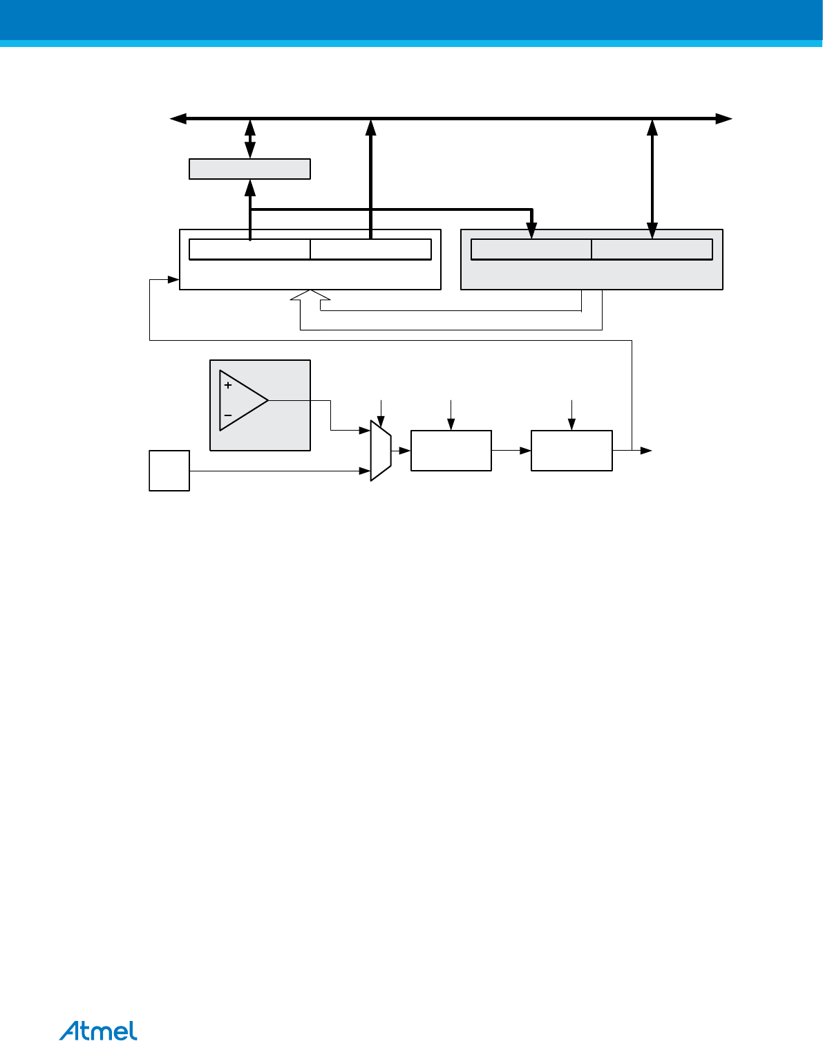
Figure 21-3 Input Capture Unit Block Diagram
ICFn (Int.Req.)
Analog
Comparator
WRITE ICRn (16-bit Register)
ICRnH (8-bit)
Noise
Canceler
ICPn
Edge
Detector
TEMP (8-bit)
DATA BUS (8-bit)
ICRnL (8-bit)
TCNTn (16-bit Counter)
TCNTnH (8-bit) TCNTnL (8-bit)
ACIC* ICNC ICES
ACO*
When a change of the logic level (an event) occurs on the Input Capture Pin (ICP1), alternatively on the
Analog Comparator Output (ACO), and this change confirms to the setting of the edge detector, a capture
will be triggered. When a capture is triggered, the 16-bit value of the counter (TCNT1) is written to the
Input Capture Register (ICR1). The Input Capture Flag (ICF1) is set at the same system clock as the
TCNT1 value is copied into ICR1 Register. If enabled (TICIE1 = 1), the Input Capture Flag generates an
Input Capture interrupt. The ICF1 Flag is automatically cleared when the interrupt is executed.
Alternatively the ICF1 Flag can be cleared by software by writing a logical one to its I/O bit location.
Reading the 16-bit value in the Input Capture Register (ICR1) is done by first reading the Low byte
(ICR1L) and then the High byte (ICR1H). When the Low byte is read the High byte is copied into the High
byte temporary register (TEMP). When the CPU reads the ICR1H I/O location it will access the TEMP
Register.
The ICR1 Register can only be written when using a Waveform Generation mode that utilizes the ICR1
Register for defining the counter’s TOP value. In these cases the Waveform Generation mode
(WGM13:0) bits must be set before the TOP value can be written to the ICR1 Register. When writing the
ICR1 Register the High byte must be written to the ICR1H I/O location before the Low byte is written to
ICR1L.
For more information on how to access the 16-bit registers refer to Accessing 16-bit Registers on page
17.
21.6.1. Input Capture Pin Source
The main trigger source for the Input Capture unit is the Input Capture Pin (ICP1). Timer/Counter 1 can
alternatively use the Analog Comparator Output as trigger source for the Input Capture unit. The Analog
Comparator is selected as trigger source by setting the Analog Comparator Input Capture (ACIC) bit in
the Analog Comparator Control and Status Register (ACSR). Be aware that changing trigger source can
trigger a capture. The Input Capture Flag must therefore be cleared after the change.
Atmel ATmega8A [DATASHEET]
Atmel-8159F-8-bit AVR Microcontroller_Datasheet_Complete-09/2015
118

Both the Input Capture Pin (ICP1) and the Analog Comparator Output (ACO) inputs are sampled using
the same technique as for the T1 pin (see figure T1 Pin Sampling in section External Clock Source). The
edge detector is also identical. However, when the noise canceler is enabled, additional logic is inserted
before the edge detector, which increases the delay by four system clock cycles. Note that the input of the
noise canceler and edge detector is always enabled unless the Timer/Counter is set in a Waveform
Generation mode that uses ICR1 to define TOP.
An Input Capture can be triggered by software by controlling the port of the ICP1 pin.
Related Links
External Clock Source on page 108
21.6.2. Noise Canceler
The noise canceler improves noise immunity by using a simple digital filtering scheme. The noise
canceler input is monitored over four samples, and all four must be equal for changing the output that in
turn is used by the edge detector.
The noise canceler is enabled by setting the Input Capture Noise Canceler (ICNC1) bit in Timer/Counter
Control Register B (TCCR1B). When enabled the noise canceler introduces additional four system clock
cycles of delay from a change applied to the input, to the update of the ICR1 Register. The noise canceler
uses the system clock and is therefore not affected by the prescaler.
21.6.3. Using the Input Capture Unit
The main challenge when using the Input Capture unit is to assign enough processor capacity for
handling the incoming events. The time between two events is critical. If the processor has not read the
captured value in the ICR1 Register before the next event occurs, the ICR1 will be overwritten with a new
value. In this case the result of the capture will be incorrect.
When using the Input Capture interrupt, the ICR1 Register should be read as early in the interrupt handler
routine as possible. Even though the Input Capture interrupt has relatively high priority, the maximum
interrupt response time is dependent on the maximum number of clock cycles it takes to handle any of
the other interrupt requests.
Using the Input Capture unit in any mode of operation when the TOP value (resolution) is actively
changed during operation, is not recommended.
Measurement of an external signal’s duty cycle requires that the trigger edge is changed after each
capture. Changing the edge sensing must be done as early as possible after the ICR1 Register has been
read. After a change of the edge, the Input Capture Flag (ICF1) must be cleared by software (writing a
logical one to the I/O bit location). For measuring frequency only, the clearing of the ICF1 Flag is not
required (if an interrupt handler is used).
21.7. Output Compare Units
The 16-bit comparator continuously compares TCNT1 with the Output Compare Register (OCR1x). If
TCNT equals OCR1x the comparator signals a match. A match will set the Output Compare Flag
(OCF1x) at the next timer clock cycle. If enabled (OCIE1x = 1), the Output Compare Flag generates an
Output Compare interrupt. The OCF1x Flag is automatically cleared when the interrupt is executed.
Alternatively the OCF1x Flag can be cleared by software by writing a logical one to its I/O bit location. The
waveform generator uses the match signal to generate an output according to operating mode set by the
Waveform Generation mode (WGM13:0) bits and Compare Output mode (COM1x1:0) bits. The TOP and
BOTTOM signals are used by the waveform generator for handling the special cases of the extreme
values in some modes of operation (See Modes of Operation on page 122.)
Atmel ATmega8A [DATASHEET]
Atmel-8159F-8-bit AVR Microcontroller_Datasheet_Complete-09/2015
119
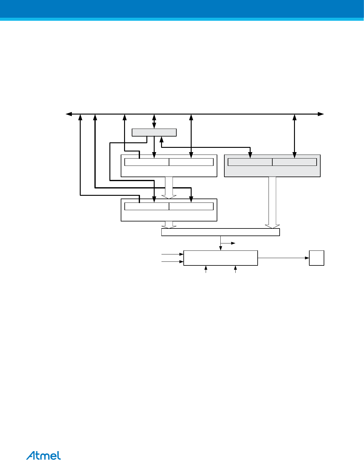
A special feature of Output Compare unit A allows it to define the Timer/Counter TOP value (i.e. counter
resolution). In addition to the counter resolution, the TOP value defines the period time for waveforms
generated by the waveform generator.
The figure below shows a block diagram of the Output Compare unit. The small “n” in the register and bit
names indicates the device number (n = 1 for Timer/Counter 1), and the “x” indicates Output Compare
unit (A/B). The elements of the block diagram that are not directly a part of the Output Compare unit are
gray shaded.
Figure 21-4 Output Compare Unit, Block Diagram
OCFnx (Int.Req.)
= (16-bit Comparator )
OCRnx Buffer (16-bit Register)
OCRnxH Buf. (8-bit)
OCnx
TEMP (8-bit)
DATA BUS (8-bit)
OCRnxL Buf. (8-bit)
TCNTn (16-bit Counter)
TCNTnH (8-bit) TCNTnL (8-bit)
COMnx1:0WGMn3:0
OCRnx (16-bit Register)
OCRnxH (8-bit) OCRnxL (8-bit)
Waveform Generator
TOP
BOTTOM
The OCR1x Register is double buffered when using any of the twelve Pulse Width Modulation (PWM)
modes. For the normal and Clear Timer on Compare (CTC) modes of operation, the double buffering is
disabled. The double buffering synchronizes the update of the OCR1x Compare Register to either TOP or
BOTTOM of the counting sequence. The synchronization prevents the occurrence of odd-length, non-
symmetrical PWM pulses, thereby making the output glitch-free.
The OCR1x Register access may seem complex, but this is not case. When the double buffering is
enabled, the CPU has access to the OCR1x Buffer Register, and if double buffering is disabled the CPU
will access the OCR1x directly. The content of the OCR1x (Buffer or Compare) Register is only changed
by a write operation (the Timer/Counter does not update this register automatically as the TCNT1 and
ICR1 Register). Therefore OCR1x is not read via the High byte temporary register (TEMP). However, it is
a good practice to read the Low byte first as when accessing other 16-bit registers. Writing the OCR1x
Registers must be done via the TEMP Register since the compare of all 16-bit is done continuously. The
High byte (OCR1xH) has to be written first. When the High byte I/O location is written by the CPU, the
TEMP Register will be updated by the value written. Then when the Low byte (OCR1xL) is written to the
lower eight bits, the High byte will be copied into the upper 8-bits of either the OCR1x buffer or OCR1x
Compare Register in the same system clock cycle.
For more information of how to access the 16-bit registers refer to Accessing 16-bit Registers on page 17.
Atmel ATmega8A [DATASHEET]
Atmel-8159F-8-bit AVR Microcontroller_Datasheet_Complete-09/2015
120

21.7.1. Force Output Compare
In non-PWM Waveform Generation modes, the match output of the comparator can be forced by writing a
one to the Force Output Compare (FOC1x) bit. Forcing Compare Match will not set the OCF1x Flag or
reload/clear the timer, but the OC1x pin will be updated as if a real Compare Match had occurred (the
COM1x1:0 bits settings define whether the OC1x pin is set, cleared or toggled).
21.7.2. Compare Match Blocking by TCNT1 Write
All CPU writes to the TCNT1 Register will block any Compare Match that occurs in the next timer clock
cycle, even when the timer is stopped. This feature allows OCR1x to be initialized to the same value as
TCNT1 without triggering an interrupt when the Timer/Counter clock is enabled.
21.7.3. Using the Output Compare Unit
Since writing TCNT1 in any mode of operation will block all compare matches for one timer clock cycle,
there are risks involved when changing TCNT1 when using any of the Output Compare channels,
independent of whether the Timer/Counter is running or not. If the value written to TCNT1 equals the
OCR1x value, the Compare Match will be missed, resulting in incorrect waveform generation. Do not
write the TCNT1 equal to TOP in PWM modes with variable TOP values. The Compare Match for the
TOP will be ignored and the counter will continue to 0xFFFF. Similarly, do not write the TCNT1 value
equal to BOTTOM when the counter is downcounting.
The setup of the OC1x should be performed before setting the Data Direction Register for the port pin to
output. The easiest way of setting the OC1x value is to use the Force Output Compare (FOC1x) strobe
bits in Normal mode. The OC1x Register keeps its value even when changing between Waveform
Generation modes.
Be aware that the COM1x1:0 bits are not double buffered together with the compare value. Changing the
COM1x1:0 bits will take effect immediately.
21.8. Compare Match Output Unit
The Compare Output mode (COM1x1:0) bits have two functions. The waveform generator uses the
COM1x1:0 bits for defining the Output Compare (OC1x) state at the next Compare Match. Secondly the
COM1x1:0 bits control the OC1x pin output source. The figure below shows a simplified schematic of the
logic affected by the COM1x1:0 bit setting. The I/O Registers, I/O bits, and I/O pins in the figure are
shown in bold. Only the parts of the general I/O Port Control Registers (DDR and PORT) that are affected
by the COM1x1:0 bits are shown. When referring to the OC1x state, the reference is for the internal OC1x
Register, not the OC1x pin. If a System Reset occur, the OC1x Register is reset to “0”.
Atmel ATmega8A [DATASHEET]
Atmel-8159F-8-bit AVR Microcontroller_Datasheet_Complete-09/2015
121
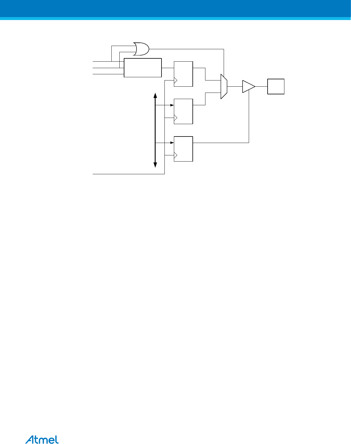
Figure 21-5 Compare Match Output Unit, Schematic
PORT
DDR
D Q
D Q
OCnx
Pin
OCnx
D Q
Waveform
Generator
COMnx1
COMnx0
0
1
DATA BUS
FOCnx
clkI/O
The general I/O port function is overridden by the Output Compare (OC1x) from the waveform generator
if either of the COM1x1:0 bits are set. However, the OC1x pin direction (input or output) is still controlled
by the Data Direction Register (DDR) for the port pin. The Data Direction Register bit for the OC1x pin
(DDR_OC1x) must be set as output before the OC1x value is visible on the pin. The port override function
is generally independent of the Waveform Generation mode, but there are some exceptions. Refer to
Table 21-2 Compare Output Mode, non-PWM on page 132, Table 21-3 Compare Output Mode, Fast
PWM(1) on page 133 and Table 21-4 Compare Output Mode, Phase Correct and Phase and Frequency
Correct PWM(1) on page 133 for details.
The design of the Output Compare Pin logic allows initialization of the OC1x state before the output is
enabled. Note that some COM1x1:0 bit settings are reserved for certain modes of operation. See
Register Description.
The COM1x1:0 bits have no effect on the Input Capture unit.
21.8.1. Compare Output Mode and Waveform Generation
The waveform generator uses the COM1x1:0 bits differently in normal, CTC, and PWM modes. For all
modes, setting the COM1x1:0 = 0 tells the waveform generator that no action on the OC1x Register is to
be performed on the next Compare Match. For compare output actions in the non-PWM modes refer to
Table 21-2 Compare Output Mode, non-PWM on page 132. For fast PWM mode refer to Table 21-3
Compare Output Mode, Fast PWM(1) on page 133, and for phase correct and phase and frequency
correct PWM refer to Table 21-4 Compare Output Mode, Phase Correct and Phase and Frequency
Correct PWM(1) on page 133.
A change of the COM1x1:0 bits state will have effect at the first Compare Match after the bits are written.
For nonPWM modes, the action can be forced to have immediate effect by using the FOC1x strobe bits.
21.9. Modes of Operation
The mode of operation (i.e., the behavior of the Timer/Counter and the Output Compare pins) is defined
by the combination of the Waveform Generation mode (WGM13:0) and Compare Output mode
(COM1x1:0) bits. The Compare Output mode bits do not affect the counting sequence, while the
Waveform Generation mode bits do. The COM1x1:0 bits control whether the PWM output generated
should be inverted or not (inverted or non-inverted PWM). For non-PWM modes the COM1x1:0 bits
Atmel ATmega8A [DATASHEET]
Atmel-8159F-8-bit AVR Microcontroller_Datasheet_Complete-09/2015
122
control whether the output should be set, cleared or toggle at a Compare Match. See Compare Match
Output Unit on page 121.
For detailed timing information refer to Timer/Counter Timing Diagrams on page 130.
21.9.1. Normal Mode
The simplest mode of operation is the Normal mode (WGM13:0 = 0). In this mode the counting direction
is always up (incrementing), and no counter clear is performed. The counter simply overruns when it
passes its maximum 16-bit value (MAX = 0xFFFF) and then restarts from the BOTTOM (0x0000). In
normal operation the Timer/Counter Overflow Flag (TOV1) will be set in the same timer clock cycle as the
TCNT1 becomes zero. The TOV1 Flag in this case behaves like a 17th bit, except that it is only set, not
cleared. However, combined with the timer overflow interrupt that automatically clears the TOV1 Flag, the
timer resolution can be increased by software. There are no special cases to consider in the Normal
mode, a new counter value can be written anytime.
The Input Capture unit is easy to use in Normal mode. However, observe that the maximum interval
between the external events must not exceed the resolution of the counter. If the interval between events
are too long, the timer overflow interrupt or the prescaler must be used to extend the resolution for the
capture unit.
The Output Compare units can be used to generate interrupts at some given time. Using the Output
Compare to generate waveforms in Normal mode is not recommended, since this will occupy too much of
the CPU time.
21.9.2. Clear Timer on Compare Match (CTC) Mode
In Clear Timer on Compare or CTC mode (WGM13:0 = 4 or 12), the OCR1A or ICR1 Register are used to
manipulate the counter resolution. In CTC mode the counter is cleared to zero when the counter value
(TCNT1) matches either the OCR1A (WGM13:0 = 4) or the ICR1 (WGM13:0 = 12). The OCR1A or ICR1
define the top value for the counter, hence also its resolution. This mode allows greater control of the
Compare Match output frequency. It also simplifies the operation of counting external events.
The timing diagram for the CTC mode is shown below. The counter value (TCNT1) increases until a
Compare Match occurs with either OCR1A or ICR1, and then counter (TCNT1) is cleared.
Figure 21-6 CTC Mode, Timing Diagram
TCNTn
OCnA
(Toggle)
OCnA Interrupt Flag Set
or ICFn Interrupt Flag Set
(Interrupt on TOP)
1 4
Period 2 3
(COMnA1:0 = 1)
An interrupt can be generated at each time the counter value reaches the TOP value by either using the
OCF1A or ICF1 Flag according to the register used to define the TOP value. If the interrupt is enabled,
the interrupt handler routine can be used for updating the TOP value. However, changing the TOP to a
value close to BOTTOM when the counter is running with none or a low prescaler value must be done
with care since the CTC mode does not have the double buffering feature. If the new value written to
OCR1A or ICR1 is lower than the current value of TCNT1, the counter will miss the Compare Match. The
counter will then have to count to its maximum value (0xFFFF) and wrap around starting at 0x0000 before
the Compare Match can occur. In many cases this feature is not desirable. An alternative will then be to
Atmel ATmega8A [DATASHEET]
Atmel-8159F-8-bit AVR Microcontroller_Datasheet_Complete-09/2015
123
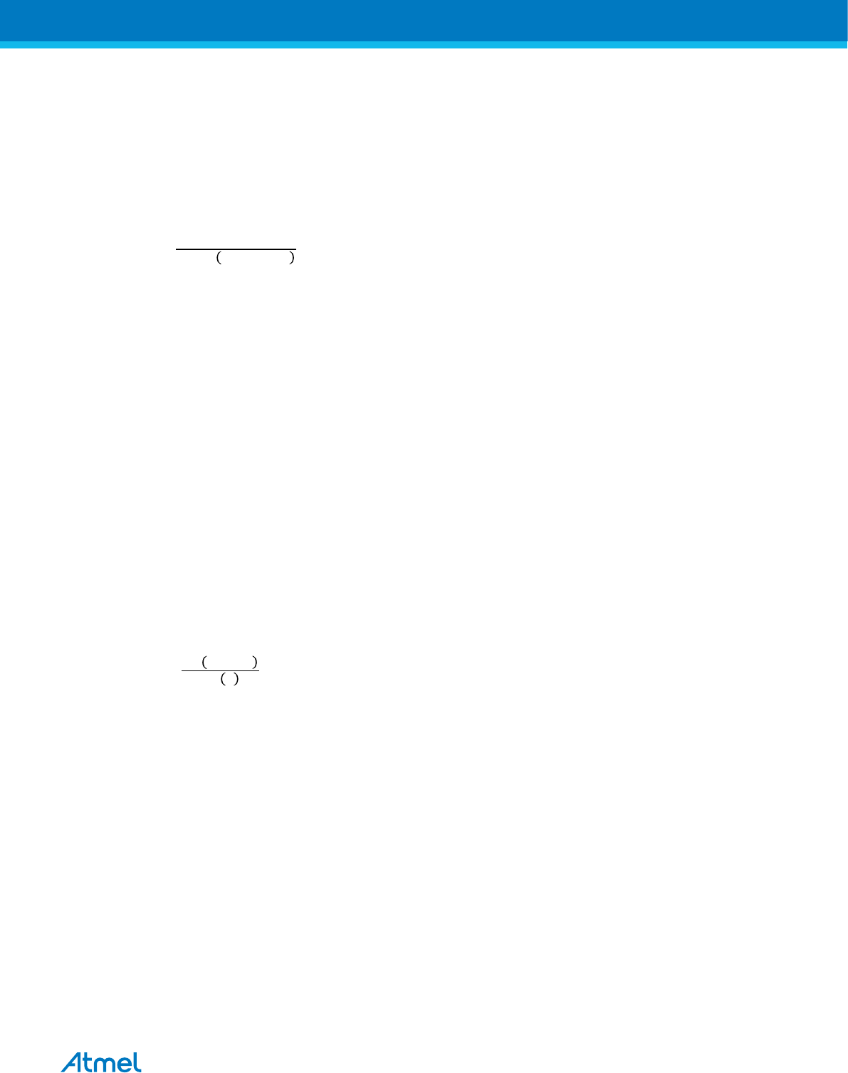
use the fast PWM mode using OCR1A for defining TOP (WGM13:0 = 15) since the OCR1A then will be
double buffered.
For generating a waveform output in CTC mode, the OC1A output can be set to toggle its logical level on
each Compare Match by setting the Compare Output mode bits to toggle mode (COM1A1:0 = 1). The
OC1A value will not be visible on the port pin unless the data direction for the pin is set to output
(DDR_OC1A = 1). The waveform generated will have a maximum frequency of fOC1A = fclk_I/O/2 when
OCR1A is set to zero (0x0000). The waveform frequency is defined by the following equation:
OCnA =clk_I/O
2 1 + OCRnA
N represents the prescaler factor (1, 8, 64, 256, or 1024).
As for the Normal mode of operation, the Timer Counter TOV1 Flag is set in the same timer clock cycle
that the counter counts from MAX to 0x0000.
21.9.3. Fast PWM Mode
The fast Pulse Width Modulation or fast PWM mode (WGM13:0 = 5, 6, 7, 14, or 15) provides a high
frequency PWM waveform generation option. The fast PWM differs from the other PWM options by its
single-slope operation. The counter counts from BOTTOM to TOP then restarts from BOTTOM. In non-
inverting Compare Output mode, the Output Compare (OC1x) is cleared on the Compare Match between
TCNT1 and OCR1x, and set at BOTTOM. In inverting Compare Output mode output is set on Compare
Match and cleared at BOTTOM. Due to the singleslope operation, the operating frequency of the fast
PWM mode can be twice as high as the phase correct and phase and frequency correct PWM modes that
use dual-slope operation. This high frequency makes the fast PWM mode well suited for power
regulation, rectification, and DAC applications. High frequency allows physically small sized external
components (coils, capacitors), hence reduces total system cost.
The PWM resolution for fast PWM can be fixed to 8-, 9-, or 10-bit, or defined by either ICR1 or OCR1A.
The minimum resolution allowed is 2-bit (ICR1 or OCR1A set to 0x0003), and the maximum resolution is
16-bit (ICR1 or OCR1A set to MAX). The PWM resolution in bits can be calculated by using the following
equation:
FPWM =log TOP+1
log 2
In fast PWM mode the counter is incremented until the counter value matches either one of the fixed
values 0x00FF, 0x01FF, or 0x03FF (WGM13:0 = 5, 6, or 7), the value in ICR1 (WGM13:0 = 14), or the
value in OCR1A (WGM13:0 = 15). The counter is then cleared at the following timer clock cycle. The
timing diagram for the fast PWM mode is shown in the figure below. The figure shows fast PWM mode
when OCR1A or ICR1 is used to define TOP. The TCNT1 value is in the timing diagram shown as a
histogram for illustrating the single-slope operation. The diagram includes non-inverted and inverted
PWM outputs. The small horizontal line marks on the TCNT1 slopes represent compare matches
between OCR1x and TCNT1. The OC1x Interrupt Flag will be set when a Compare Match occurs.
Atmel ATmega8A [DATASHEET]
Atmel-8159F-8-bit AVR Microcontroller_Datasheet_Complete-09/2015
124
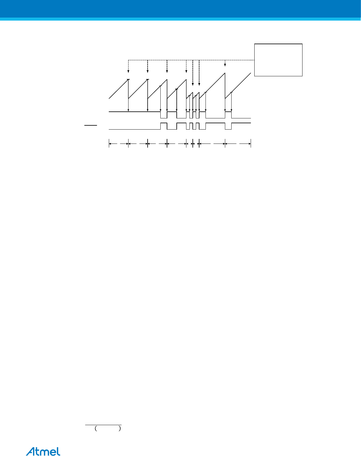
Figure 21-7 Fast PWM Mode, Timing Diagram
TCNTn
OCRnx/TOP Update and
TOVn Interrupt Flag Set and
OCnA Interrupt Flag Set
or ICFn Interrupt Flag Set
(Interrupt on TOP)
1 7
Period 2 3 4 5 6 8
OCnx
OCnx
(COMnx1:0 = 2)
(COMnx1:0 = 3)
The Timer/Counter Overflow Flag (TOV1) is set each time the counter reaches TOP. In addition the
OCF1A or ICF1 Flag is set at the same timer clock cycle as TOV1 is set when either OCR1A or ICR1 is
used for defining the TOP value. If one of the interrupts are enabled, the interrupt handler routine can be
used for updating the TOP and compare values.
When changing the TOP value the program must ensure that the new TOP value is higher or equal to the
value of all of the Compare Registers. If the TOP value is lower than any of the Compare Registers, a
Compare Match will never occur between the TCNT1 and the OCR1x. Note that when using fixed TOP
values the unused bits are masked to zero when any of the OCR1x Registers are written.
The procedure for updating ICR1 differs from updating OCR1A when used for defining the TOP value.
The ICR1 Register is not double buffered. This means that if ICR1 is changed to a low value when the
counter is running with none or a low prescaler value, there is a risk that the new ICR1 value written is
lower than the current value of TCNT1. The result will then be that the counter will miss the Compare
Match at the TOP value. The counter will then have to count to the MAX value (0xFFFF) and wrap around
starting at 0x0000 before the Compare Match can occur. The OCR1A Register, however, is double
buffered. This feature allows the OCR1A I/O location to be written anytime. When the OCR1A I/O location
is written the value written will be put into the OCR1A Buffer Register. The OCR1A Compare Register will
then be updated with the value in the Buffer Register at the next timer clock cycle the TCNT1 matches
TOP. The update is done at the same timer clock cycle as the TCNT1 is cleared and the TOV1 Flag is
set.
Using the ICR1 Register for defining TOP works well when using fixed TOP values. By using ICR1, the
OCR1A Register is free to be used for generating a PWM output on OC1A. However, if the base PWM
frequency is actively changed (by changing the TOP value), using the OCR1A as TOP is clearly a better
choice due to its double buffer feature.
In fast PWM mode, the compare units allow generation of PWM waveforms on the OC1x pins. Setting the
COM1x1:0 bits to 2 will produce a non-inverted PWM and an inverted PWM output can be generated by
setting the COM1x1:0 to 3. Refer to table Table 21-3 Compare Output Mode, Fast PWM(1) on page 133.
The actual OC1x value will only be visible on the port pin if the data direction for the port pin is set as
output (DDR_OC1x). The PWM waveform is generated by setting (or clearing) the OC1x Register at the
Compare Match between OCR1x and TCNT1, and clearing (or setting) the OC1x Register at the timer
clock cycle the counter is cleared (changes from TOP to BOTTOM).
The PWM frequency for the output can be calculated by the following equation:
OCnxPWM =clk_I/O
1 + TOP
Atmel ATmega8A [DATASHEET]
Atmel-8159F-8-bit AVR Microcontroller_Datasheet_Complete-09/2015
125

N represents the prescale divider (1, 8, 64, 256, or 1024).
The extreme values for the OCR1x Register represents special cases when generating a PWM waveform
output in the fast PWM mode. If the OCR1x is set equal to BOTTOM (0x0000) the output will be a narrow
spike for each TOP+1 timer clock cycle. Setting the OCR1x equal to TOP will result in a constant high or
low output (depending on the polarity of the output set by the COM1x1:0 bits.)
A frequency (with 50% duty cycle) waveform output in fast PWM mode can be achieved by setting OC1A
to toggle its logical level on each Compare Match (COM1A1:0 = 1). This applies only if OCR1A is used to
define the TOP value (WGM13:0 = 15). The waveform generated will have a maximum frequency of fOC1A
= fclk_I/O/2 when OCR1A is set to zero (0x0000). This feature is similar to the OC1A toggle in CTC mode,
except the double buffer feature of the Output Compare unit is enabled in the fast PWM mode.
21.9.4. Phase Correct PWM Mode
The phase correct Pulse Width Modulation or phase correct PWM mode (WGM13:0 = 1, 2, 3, 10, or 11)
provides a high resolution phase correct PWM waveform generation option. The phase correct PWM
mode is, like the phase and frequency correct PWM mode, based on a dual-slope operation. The counter
counts repeatedly from BOTTOM (0x0000) to TOP and then from TOP to BOTTOM. In non-inverting
Compare Output mode, the Output Compare (OC1x) is cleared on the Compare Match between TCNT1
and OCR1x while upcounting, and set on the Compare Match while downcounting. In inverting Output
Compare mode, the operation is inverted. The dual-slope operation has lower maximum operation
frequency than single slope operation. However, due to the symmetric feature of the dual-slope PWM
modes, these modes are preferred for motor control applications.
The PWM resolution for the phase correct PWM mode can be fixed to 8-, 9-, or 10-bit, or defined by either
ICR1 or OCR1A. The minimum resolution allowed is 2-bit (ICR1 or OCR1A set to 0x0003), and the
maximum resolution is 16-bit (ICR1 or OCR1A set to MAX). The PWM resolution in bits can be calculated
by using the following equation:
PCPWM =log TOP+1
log 2
In phase correct PWM mode the counter is incremented until the counter value matches either one of the
fixed values 0x00FF, 0x01FF, or 0x03FF (WGM13:0 = 1, 2, or 3), the value in ICR1 (WGM13:0 = 10), or
the value in OCR1A (WGM13:0 = 11). The counter has then reached the TOP and changes the count
direction. The TCNT1 value will be equal to TOP for one timer clock cycle. The timing diagram for the
phase correct PWM mode is shown in the figure below. The figure shows phase correct PWM mode when
OCR1A or ICR1 is used to define TOP. The TCNT1 value is in the timing diagram shown as a histogram
for illustrating the dual-slope operation. The diagram includes non-inverted and inverted PWM outputs.
The small horizontal line marks on the TCNT1 slopes represent compare matches between OCR1x and
TCNT1. The OC1x Interrupt Flag will be set when a Compare Match occurs.
Atmel ATmega8A [DATASHEET]
Atmel-8159F-8-bit AVR Microcontroller_Datasheet_Complete-09/2015
126
Figure 21-8 Phase Correct PWM Mode, Timing Diagram
OCRnx/TOP Update and
OCnA Interrupt Flag Set
or ICFn Interrupt Flag Set
(Interrupt on TOP)
1 2 3 4
TOVn Interrupt Flag Set
(Interrupt on Bottom)
TCNTn
Period
OCnx
OCnx
(COMnx1:0 = 2)
(COMnx1:0 = 3)
The Timer/Counter Overflow Flag (TOV1) is set each time the counter reaches BOTTOM. When either
OCR1A or ICR1 is used for defining the TOP value, the OC1A or ICF1 Flag is set accordingly at the same
timer clock cycle as the OCR1x Registers are updated with the double buffer value (at TOP). The
Interrupt Flags can be used to generate an interrupt each time the counter reaches the TOP or BOTTOM
value.
When changing the TOP value the program must ensure that the new TOP value is higher or equal to the
value of all of the Compare Registers. If the TOP value is lower than any of the Compare Registers, a
Compare Match will never occur between the TCNT1 and the OCR1x. Note that when using fixed TOP
values, the unused bits are masked to zero when any of the OCR1x Registers are written. As the third
period shown in the timing diagram above illustrates, changing the TOP actively while the Timer/Counter
is running in the Phase Correct mode can result in an unsymmetrical output. The reason for this can be
found in the time of update of the OCR1x Register. Since the OCR1x update occurs at TOP, the PWM
period starts and ends at TOP. This implies that the length of the falling slope is determined by the
previous TOP value, while the length of the rising slope is determined by the new TOP value. When these
two values differ the two slopes of the period will differ in length. The difference in length gives the
unsymmetrical result on the output.
It is recommended to use the Phase and Frequency Correct mode instead of the Phase Correct mode
when changing the TOP value while the Timer/Counter is running. When using a static TOP value there
are practically no differences between the two modes of operation.
In phase correct PWM mode, the compare units allow generation of PWM waveforms on the OC1x pins.
Setting the COM1x1:0 bits to 2 will produce a non-inverted PWM and an inverted PWM output can be
generated by setting the COM1x1:0 to 3. Refer to Table 21-4 Compare Output Mode, Phase Correct and
Phase and Frequency Correct PWM(1) on page 133. The actual OC1x value will only be visible on the
port pin if the data direction for the port pin is set as output (DDR_OC1x). The PWM waveform is
generated by setting (or clearing) the OC1x Register at the Compare Match between OCR1x and TCNT1
when the counter increments, and clearing (or setting) the OC1x Register at Compare Match between
OCR1x and TCNT1 when the counter decrements. The PWM frequency for the output when using phase
correct PWM can be calculated by the following equation:
OCnxPCPWM =clk_I/O
2 TOP
N variable represents the prescale divider (1, 8, 64, 256, or 1024).
Atmel ATmega8A [DATASHEET]
Atmel-8159F-8-bit AVR Microcontroller_Datasheet_Complete-09/2015
127

The extreme values for the OCR1x Register represent special cases when generating a PWM waveform
output in the phase correct PWM mode. If the OCR1x is set equal to BOTTOM the output will be
continuously low and if set equal to TOP the output will be continuously high for non-inverted PWM mode.
For inverted PWM the output will have the opposite logic values.
If OCR1A is used to define the TOP value (WGM13:0 = 11) and COM1A1:0 = 1, the OC1A output will
toggle with a 50% duty cycle.
21.9.5. Phase and Frequency Correct PWM Mode
The phase and frequency correct Pulse Width Modulation, or phase and frequency correct PWM mode
(WGM13:0 = 8 or 9) provides a high resolution phase and frequency correct PWM waveform generation
option. The phase and frequency correct PWM mode is, like the phase correct PWM mode, based on a
dual-slope operation. The counter counts repeatedly from BOTTOM (0x0000) to TOP and then from TOP
to BOTTOM. In non-inverting Compare Output mode, the Output Compare (OC1x) is cleared on the
Compare Match between TCNT1 and OCR1x while upcounting, and set on the Compare Match while
downcounting. In inverting Compare Output mode, the operation is inverted. The dual-slope operation
gives a lower maximum operation frequency compared to the single-slope operation. However, due to the
symmetric feature of the dual-slope PWM modes, these modes are preferred for motor control
applications.
The main difference between the phase correct, and the phase and frequency correct PWM mode is the
time the OCR1x Register is updated by the OCR1x Buffer Register, (see Figure 21-8 Phase Correct
PWM Mode, Timing Diagram on page 127 and Figure 21-9 Phase and Frequency Correct PWM Mode,
Timing Diagram on page 129).
The PWM resolution for the phase and frequency correct PWM mode can be defined by either ICR1 or
OCR1A. The minimum resolution allowed is 2-bit (ICR1 or OCR1A set to 0x0003), and the maximum
resolution is 16-bit (ICR1 or OCR1A set to MAX). The PWM resolution in bits can be calculated using the
following equation:
PFCPWM =log TOP+1
log 2
In phase and frequency correct PWM mode the counter is incremented until the counter value matches
either the value in ICR1 (WGM13:0 = 8), or the value in OCR1A (WGM13:0 = 9). The counter has then
reached the TOP and changes the count direction. The TCNT1 value will be equal to TOP for one timer
clock cycle. The timing diagram for the phase correct and frequency correct PWM mode is shown on
timing diagram below. The figure shows phase and frequency correct PWM mode when OCR1A or ICR1
is used to define TOP. The TCNT1 value is in the timing diagram shown as a histogram for illustrating the
dual-slope operation. The diagram includes non-inverted and inverted PWM outputs. The small horizontal
line marks on the TCNT1 slopes represent compare matches between OCR1x and TCNT1. The OC1x
Interrupt Flag will be set when a Compare Match occurs.
Atmel ATmega8A [DATASHEET]
Atmel-8159F-8-bit AVR Microcontroller_Datasheet_Complete-09/2015
128
Figure 21-9 Phase and Frequency Correct PWM Mode, Timing Diagram
OCRnx/TOP Updateand
TOVn Interrupt Flag Set
(Interrupt on Bottom)
OCnA Interrupt Flag Set
or ICFn Interrupt Flag Set
(Interrupt on TOP)
1 2 3 4
TCNTn
Period
OCnx
OCnx
(COMnx1:0 = 2)
(COMnx1:0 = 3)
The Timer/Counter Overflow Flag (TOV1) is set at the same timer clock cycle as the OCR1x Registers
are updated with the double buffer value (at BOTTOM). When either OCR1A or ICR1 is used for defining
the TOP value, the OC1A or ICF1 Flag set when TCNT1 has reached TOP. The Interrupt Flags can then
be used to generate an interrupt each time the counter reaches the TOP or BOTTOM value.
When changing the TOP value the program must ensure that the new TOP value is higher or equal to the
value of all of the Compare Registers. If the TOP value is lower than any of the Compare Registers, a
Compare Match will never occur between the TCNT1 and the OCR1x.
As the timing diagram above shows the output generated is, in contrast to the Phase Correct mode,
symmetrical in all periods. Since the OCR1x Registers are updated at BOTTOM, the length of the rising
and the falling slopes will always be equal. This gives symmetrical output pulses and is therefore
frequency correct.
Using the ICR1 Register for defining TOP works well when using fixed TOP values. By using ICR1, the
OCR1A Register is free to be used for generating a PWM output on OC1A. However, if the base PWM
frequency is actively changed by changing the TOP value, using the OCR1A as TOP is clearly a better
choice due to its double buffer feature.
In phase and frequency correct PWM mode, the compare units allow generation of PWM waveforms on
the OC1x pins. Setting the COM1x1:0 bits to 2 will produce a non-inverted PWM and an inverted PWM
output can be generated by setting the COM1x1:0 to 3. Refer to Table 21-4 Compare Output Mode,
Phase Correct and Phase and Frequency Correct PWM(1) on page 133. The actual OC1x value will only
be visible on the port pin if the data direction for the port pin is set as output (DDR_OC1x). The PWM
waveform is generated by setting (or clearing) the OC1x Register at the Compare Match between OCR1x
and TCNT1 when the counter increments, and clearing (or setting) the OC1x Register at Compare Match
between OCR1x and TCNT1 when the counter decrements. The PWM frequency for the output when
using phase and frequency correct PWM can be calculated by the following equation:
OCnxPFCPWM =clk_I/O
2 TOP
The N variable represents the prescaler divider (1, 8, 64, 256, or 1024).
The extreme values for the OCR1x Register represents special cases when generating a PWM waveform
output in the phase correct PWM mode. If the OCR1x is set equal to BOTTOM the output will be
Atmel ATmega8A [DATASHEET]
Atmel-8159F-8-bit AVR Microcontroller_Datasheet_Complete-09/2015
129
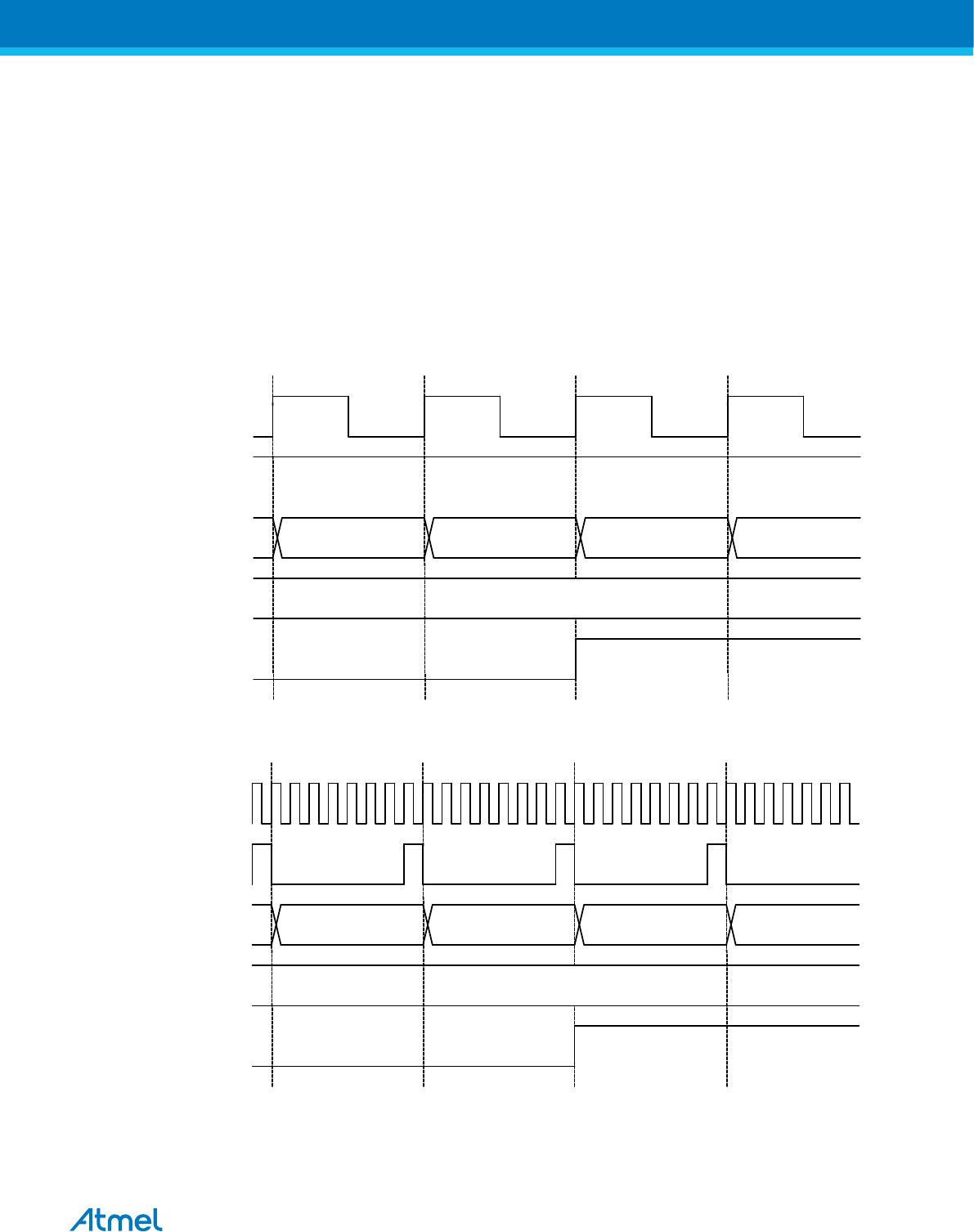
continuously low and if set equal to TOP the output will be set to high for non-inverted PWM mode. For
inverted PWM the output will have the opposite logic values.
If OCR1A is used to define the TOP value (WGM13:0 = 9) and COM1A1:0 = 1, the OC1A output will
toggle with a 50% duty cycle.
21.10. Timer/Counter Timing Diagrams
The Timer/Counter is a synchronous design and the timer clock (clkT1) is therefore shown as a clock
enable signal in the following figures. The figures include information on when Interrupt Flags are set, and
when the OCR1x Register is updated with the OCR1x buffer value (only for modes utilizing double
buffering). The next figure shows a timing diagram for the setting of OCF1x.
Figure 21-10 Timer/Counter Timing Diagram, Setting of OCF1x, no Prescaling
clkTn
(clkI/O/1)
OCFnx
clkI/O
OCRnx
TCNTn
OCRnx Value
OCRnx - 1 OCRnx OCRnx + 1 OCRnx + 2
The next figure shows the same timing data, but with the prescaler enabled.
Figure 21-11 Timer/Counter Timing Diagram, Setting of OCF1x, with Prescaler (fclk_I/O/8)
OCFnx
OCRnx
TCNTn
OCRnx Value
OCRnx - 1 OCRnx OCRnx + 1 OCRnx + 2
clkI/O
clkTn
(clkI/O/8)
The next figure shows the count sequence close to TOP in various modes. When using phase and
frequency correct PWM mode the OCR1x Register is updated at BOTTOM. The timing diagrams will be
the same, but TOP should be replaced by BOTTOM, TOP-1 by BOTTOM+1 and so on. The same
renaming applies for modes that set the TOV1 Flag at BOTTOM.
Atmel ATmega8A [DATASHEET]
Atmel-8159F-8-bit AVR Microcontroller_Datasheet_Complete-09/2015
130
Figure 21-12 Timer/Counter Timing Diagram, no Prescaling.
TOVn (FPWM)
and ICF n (if used
as TOP)
OCRnx
(Update at TOP)
TCNTn
(CTC and FPWM)
TCNTn
(PC and PFC PWM) TOP - 1 TOP TOP - 1 TOP - 2
Old OCRnx Value New OCRnx Value
TOP - 1 TOP BOTTOM BOTTOM + 1
clkTn
(clkI/O/1)
clkI/O
The next figure shows the same timing data, but with the prescaler enabled.
Figure 21-13 Timer/Counter Timing Diagram, with Prescaler (fclk_I/O/8)
TOVn (FPWM)
and ICF n (if used
as TOP)
OCRnx
(Update at TOP)
TCNTn
(CTC and FPWM)
TCNTn
(PC and PFC PWM) TOP - 1 TOP TOP - 1 TOP - 2
Old OCRnx Value New OCRnx Value
TOP - 1 TOP BOTTOM BOTTOM + 1
clk
I/O
clk
Tn
(clk
I/O
/8)
21.11. Register Description
Atmel ATmega8A [DATASHEET]
Atmel-8159F-8-bit AVR Microcontroller_Datasheet_Complete-09/2015
131
21.11.1. TCCR1A – Timer/Counter1 Control Register A
When using the I/O specific commands IN and OUT, the I/O addresses 0x00 - 0x3F must be used. When
addressing I/O Registers as data space using LD and ST instructions, 0x20 must be added to these offset
addresses. The device is a complex microcontroller with more peripheral units than can be supported
within the 64 location reserved in Opcode for the IN and OUT instructions. For the Extended I/O space
from 0x60 in SRAM, only the ST/STS/STD and LD/LDS/LDD instructions can be used.
Name: TCCR1A
Offset: 0x2F
Reset: 0x00
Property:
When addressing I/O Registers as data space the offset address is 0x4F
Bit 7 6 5 4 3 2 1 0
COM1A1 COM1A0 COM1B1 COM1B0 FOC1A FOC1B WGM11 WGM10
Access R/W R/W R/W R/W W W R/W R/W
Reset 0 0 0 0 0 0 0 0
Bits 7:6 – COM1An: Compare Output Mode for Channel A [n = 1:0]
Bits 5:4 – COM1Bn: Compare Output Mode for Channel B [n = 1:0]
The COM1A1:0 and COM1B1:0 control the Output Compare pins (OC1A and OC1B respectively)
behavior. If one or both of the COM1A1:0 bits are written to one, the OC1A output overrides the normal
port functionality of the I/O pin it is connected to. If one or both of the COM1B1:0 bit are written to one,
the OC1B output overrides the normal port functionality of the I/O pin it is connected to. However, note
that the Data Direction Register (DDR) bit corresponding to the OC1A or OC1B pin must be set in order
to enable the output driver.
When the OC1A or OC1B is connected to the pin, the function of the COM1n1:0 bits is dependent of the
WGM13:0 bits setting. The table below shows the COM1n1:0 bit functionality when the WGM13:0 bits are
set to a Normal or a CTC mode (non-PWM).
Table 21-2 Compare Output Mode, non-PWM
COM1A1/COM1B1 COM1A0/COM1B0 Description
0 0 Normal port operation, OC1A/OC1B disconnected.
0 1 Toggle OC1A/OC1B on Compare Match.
1 0 Clear OC1A/OC1B on Compare Match (Set output to low
level).
1 1 Set OC1A/OC1B on Compare Match (Set output to high
level).
The next table shows the COM1x1:0 bit functionality when the WGM13:0 bits are set to the fast PWM
mode.
Atmel ATmega8A [DATASHEET]
Atmel-8159F-8-bit AVR Microcontroller_Datasheet_Complete-09/2015
132

Table 21-3 Compare Output Mode, Fast PWM(1)
COM1A1/
COM1B1
COM1A0/
COM1B0
Description
0 0 Normal port operation, OC1A/OC1B disconnected.
0 1 WGM13:0 = 15: Toggle OC1A on Compare Match, OC1B
disconnected (normal port operation). For all other WGM1
settings, normal port operation, OC1A/OC1B disconnected.
1 0 Clear OC1A/OC1B on Compare Match, set OC1A/OC1B at
BOTTOM (non-inverting mode)
1 1 Set OC1A/OC1B on Compare Match, clear OC1A/OC1B at
BOTTOM (inverting mode)
Note: 1. A special case occurs when OCR1A/OCR1B equals TOP and COM1A1/COM1B1 is set. In this
case the compare match is ignored, but the set or clear is done at BOTTOM. Refer to Fast PWM Mode
on page 124 for details.
The table below shows the COM1x1:0 bit functionality when the WGM13:0 bits are set to the phase
correct or the phase and frequency correct, PWM mode.
Table 21-4 Compare Output Mode, Phase Correct and Phase and Frequency Correct PWM(1)
COM1A1/
COM1B1
COM1A0/
COM1B0
Description
0 0 Normal port operation, OC1A/OC1B disconnected.
0 1 WGM13:0 = 9 or 14: Toggle OC1A on Compare Match, OC1B
disconnected (normal port operation). For all other WGM1 settings,
normal port operation, OC1A/OC1B disconnected.
1 0 Clear OC1A/OC1B on Compare Match when up-counting. Set
OC1A/OC1B on Compare Match when down-counting.
1 1 Set OC1A/OC1B on Compare Match when up-counting. Clear
OC1A/OC1B on Compare Match when down-counting.
Note: 1. A special case occurs when OCR1A/OCR1B equals TOP and COM1A1/COM1B1 is set. Refer
to Phase Correct PWM Mode on page 126 for details.
Bit 3 – FOC1A: Force Output Compare for channel A
Bit 2 – FOC1B: Force Output Compare for channel B
The FOC1A/FOC1B bits are only active when the WGM13:0 bits specifies a non-PWM mode. However,
for ensuring compatibility with future devices, these bits must be set to zero when TCCR1A is written
when operating in a PWM mode. When writing a logical one to the FOC1A/FOC1B bit, an immediate
Compare Match is forced on the waveform generation unit. The OC1A/OC1B output is changed
according to its COM1x1:0 bits setting. Note that the FOC1A/FOC1B bits are implemented as strobes.
Therefore it is the value present in the COM1x1:0 bits that determine the effect of the forced compare.
A FOC1A/FOC1B strobe will not generate any interrupt nor will it clear the timer in Clear Timer on
Compare Match (CTC) mode using OCR1A as TOP.
The FOC1A/FOC1B bits are always read as zero.
Atmel ATmega8A [DATASHEET]
Atmel-8159F-8-bit AVR Microcontroller_Datasheet_Complete-09/2015
133
Bits 1:0 – WGM1n: Waveform Generation Mode [n = 1:0]
Combined with the WGM13:2 bits found in the TCCR1B Register, these bits control the counting
sequence of the counter, the source for maximum (TOP) counter value, and what type of waveform
generation to be used, refer to the table below. Modes of operation supported by the Timer/Counter unit
are: Normal mode (counter), Clear Timer on Compare match (CTC) mode, and three types of Pulse Width
Modulation (PWM) modes. (See Modes of Operation on page 122).
Table 21-5 Waveform Generation Mode Bit Description
Mode WGM13 WGM12
(CTC1)
WGM11
(PWM11)
WGM10
(PWM10)
Timer/Counter
Mode of Operation(1)
TOP Update of
OCR1x at
TOV1 Flag
Set on
0 0 0 0 0 Normal 0xFFFF Immediate MAX
1 0 0 0 1 PWM, Phase Correct, 8-bit 0x00FF TOP BOTTOM
2 0 0 1 0 PWM, Phase Correct, 9-bit 0x01FF TOP BOTTOM
3 0 0 1 1 PWM, Phase Correct, 10-bit 0x03FF TOP BOTTOM
4 0 1 0 0 CTC OCR1A Immediate MAX
5 0 1 0 1 Fast PWM, 8-bit 0x00FF BOTTOM TOP
6 0 1 1 0 Fast PWM, 9-bit 0x01FF BOTTOM TOP
7 0 1 1 1 Fast PWM, 10-bit 0x03FF BOTTOM TOP
8 1 0 0 0 PWM, Phase and Frequency
Correct
ICR1 BOTTOM BOTTOM
9 1 0 0 1 PWM, Phase and Frequency
Correct
OCR1A BOTTOM BOTTOM
10 1 0 1 0 PWM, Phase Correct ICR1 TOP BOTTOM
11 1 0 1 1 PWM, Phase Correct OCR1A TOP BOTTOM
12 1 1 0 0 CTC ICR1 Immediate MAX
13 1 1 0 1 Reserved - - -
14 1 1 1 0 Fast PWM ICR1 BOTTOM TOP
15 1 1 1 1 Fast PWM OCR1A BOTTOM TOP
Note:
1. The CTC1 and PWM11:0 bit definition names are obsolete. Use the WGM12:0 definitions.
However, the functionality and location of these bits are compatible with previous versions of the
timer.
Atmel ATmega8A [DATASHEET]
Atmel-8159F-8-bit AVR Microcontroller_Datasheet_Complete-09/2015
134
21.11.2. TCCR1B – Timer/Counter1 Control Register B
When using the I/O specific commands IN and OUT, the I/O addresses 0x00 - 0x3F must be used. When
addressing I/O Registers as data space using LD and ST instructions, 0x20 must be added to these offset
addresses. The device is a complex microcontroller with more peripheral units than can be supported
within the 64 location reserved in Opcode for the IN and OUT instructions. For the Extended I/O space
from 0x60 in SRAM, only the ST/STS/STD and LD/LDS/LDD instructions can be used.
Name: TCCR1B
Offset: 0x2E
Reset: 0x00
Property:
When addressing I/O Registers as data space the offset address is 0x4E
Bit 7 6 5 4 3 2 1 0
ICNC1 ICES1 WGM13 WGM12 CS12 CS11 CS10
Access R/W R/W R/W R/W R/W R/W R/W
Reset 0 0 0 0 0 0 0
Bit 7 – ICNC1: Input Capture Noise Canceler
Setting this bit (to one) activates the Input Capture Noise Canceler. When the noise canceler is activated,
the input from the Input Capture pin (ICP1) is filtered. The filter function requires four successive equal
valued samples of the ICP1 pin for changing its output. The Input Capture is therefore delayed by four
Oscillator cycles when the noise canceler is enabled.
Bit 6 – ICES1: Input Capture Edge Select
This bit selects which edge on the Input Capture pin (ICP1) that is used to trigger a capture event. When
the ICES1 bit is written to zero, a falling (negative) edge is used as trigger, and when the ICES1 bit is
written to one, a rising (positive) edge will trigger the capture.
When a capture is triggered according to the ICES1 setting, the counter value is copied into the Input
Capture Register (ICR1). The event will also set the Input Capture Flag (ICF1), and this can be used to
cause an Input Capture Interrupt, if this interrupt is enabled.
When the ICR1 is used as TOP value (see description of the WGM13:0 bits located in the TCCR1A and
the TCCR1B Register), the ICP1 is disconnected and consequently the Input Capture function is
disabled.
Bit 4 – WGM13: Waveform Generation Mode
Refer to TCCR1A.
Bit 3 – WGM12: Waveform Generation Mode
Refer to TCCR1A.
Bits 2:0 – CS1n: Clock Select [n = 0:2]
The three Clock Select bits select the clock source to be used by the Timer/Counter. Refer to figures
Timer/Counter Timing Diagram, Setting of OCF1x, no Prescaling and Timer/Counter Timing Diagram,
Setting of OCF1x, with Prescaler (fclk_I/O/8).
Atmel ATmega8A [DATASHEET]
Atmel-8159F-8-bit AVR Microcontroller_Datasheet_Complete-09/2015
135

Table 21-6 Clock Select Bit Description
CA12 CA11 CS10 Description
0 0 0 No clock source (Timer/Counter stopped).
0 0 1 clkI/O/1 (No prescaling)
0 1 0 clkI/O/8 (From prescaler)
0 1 1 clkI/O/64 (From prescaler)
1 0 0 clkI/O/256 (From prescaler)
1 0 1 clkI/O/1024 (From prescaler)
1 1 0 External clock source on T1 pin. Clock on falling edge.
1 1 1 External clock source on T1 pin. Clock on rising edge.
If external pin modes are used for the Timer/Counter1, transitions on the T1 pin will clock the counter
even if the pin is configured as an output. This feature allows software control of the counting.
Atmel ATmega8A [DATASHEET]
Atmel-8159F-8-bit AVR Microcontroller_Datasheet_Complete-09/2015
136

21.11.3. TCNT1L – Timer/Counter1 Low byte
When using the I/O specific commands IN and OUT, the I/O addresses 0x00 - 0x3F must be used. When
addressing I/O Registers as data space using LD and ST instructions, 0x20 must be added to these offset
addresses. The device is a complex microcontroller with more peripheral units than can be supported
within the 64 location reserved in Opcode for the IN and OUT instructions. For the Extended I/O space
from 0x60 in SRAM, only the ST/STS/STD and LD/LDS/LDD instructions can be used.
Name: TCNT1L
Offset: 0x2C
Reset: 0x00
Property:
When addressing I/O Registers as data space the offset address is 0x4C
Bit 7 6 5 4 3 2 1 0
TCNT1L[7:0]
Access R/W R/W R/W R/W R/W R/W R/W R/W
Reset 0 0 0 0 0 0 0 0
Bits 7:0 – TCNT1L[7:0]: Timer/Counter 1 Low byte
The two Timer/Counter I/O locations (TCNT1H and TCNT1L, combined TCNT1) give direct access, both
for read and for write operations, to the Timer/Counter unit 16-bit counter. To ensure that both the high
and low bytes are read and written simultaneously when the CPU accesses these registers, the access is
performed using an 8-bit temporary High Byte Register (TEMP). This temporary register is shared by all
the other 16-bit registers. Refer to Accessing 16-bit Registers for details.
Modifying the counter (TCNT1) while the counter is running introduces a risk of missing a compare match
between TCNT1 and one of the OCR1x Registers.
Writing to the TCNT1 Register blocks (removes) the compare match on the following timer clock for all
compare units.
Atmel ATmega8A [DATASHEET]
Atmel-8159F-8-bit AVR Microcontroller_Datasheet_Complete-09/2015
137

21.11.4. TCNT1H – Timer/Counter1 High byte
Name: TCNT1H
Offset: 0x2D
Reset: 0x00
Property:
When addressing I/O Registers as data space the offset address is 0x4D
Bit 7 6 5 4 3 2 1 0
TCNT1H[7:0]
Access R/W R/W R/W R/W R/W R/W R/W R/W
Reset 0 0 0 0 0 0 0 0
Bits 7:0 – TCNT1H[7:0]: Timer/Counter 1 High byte
Refer to TCNT1L.
Atmel ATmega8A [DATASHEET]
Atmel-8159F-8-bit AVR Microcontroller_Datasheet_Complete-09/2015
138

21.11.5. OCR1AL – Output Compare Register 1 A Low byte
When using the I/O specific commands IN and OUT, the I/O addresses 0x00 - 0x3F must be used. When
addressing I/O Registers as data space using LD and ST instructions, 0x20 must be added to these offset
addresses. The device is a complex microcontroller with more peripheral units than can be supported
within the 64 location reserved in Opcode for the IN and OUT instructions. For the Extended I/O space
from 0x60 in SRAM, only the ST/STS/STD and LD/LDS/LDD instructions can be used.
Name: OCR1AL
Offset: 0x2A
Reset: 0x00
Property:
When addressing I/O Registers as data space the offset address is 0x4A
Bit 7 6 5 4 3 2 1 0
OCR1AL[7:0]
Access R/W R/W R/W R/W R/W R/W R/W R/W
Reset 0 0 0 0 0 0 0 0
Bits 7:0 – OCR1AL[7:0]: Output Compare 1 A Low byte
The Output Compare Registers contain a 16-bit value that is continuously compared with the counter
value (TCNT1). A match can be used to generate an Output Compare interrupt, or to generate a
waveform output on the OC1x pin.
The Output Compare Registers are 16-bit in size. To ensure that both the high and low bytes are written
simultaneously when the CPU writes to these registers, the access is performed using an 8-bit temporary
High Byte Register (TEMP). This temporary register is shared by all the other 16-bit registers. Refer to
Accessing 16-bit Registers for details.
Atmel ATmega8A [DATASHEET]
Atmel-8159F-8-bit AVR Microcontroller_Datasheet_Complete-09/2015
139

21.11.6. OCR1AH – Output Compare Register 1 A High byte
Name: OCR1AH
Offset: 0x2B
Reset: 0x00
Property:
When addressing I/O Registers as data space the offset address is 0x4B
Bit 7 6 5 4 3 2 1 0
OCR1AH[7:0]
Access R/W R/W R/W R/W R/W R/W R/W R/W
Reset 0 0 0 0 0 0 0 0
Bits 7:0 – OCR1AH[7:0]: Output Compare 1 A High byte
Refer to OCR1AL.
Atmel ATmega8A [DATASHEET]
Atmel-8159F-8-bit AVR Microcontroller_Datasheet_Complete-09/2015
140

21.11.7. OCR1BL – Output Compare Register 1 B Low byte
Name: OCR1BL
Offset: 0x28
Reset: 0x00
Property:
When addressing I/O Registers as data space the offset address is 0x48
Bit 7 6 5 4 3 2 1 0
OCR1BL[7:0]
Access R/W R/W R/W R/W R/W R/W R/W R/W
Reset 0 0 0 0 0 0 0 0
Bits 7:0 – OCR1BL[7:0]: Output Compare 1 B Low byte
Refer to OCR1AL.
Atmel ATmega8A [DATASHEET]
Atmel-8159F-8-bit AVR Microcontroller_Datasheet_Complete-09/2015
141

21.11.8. OCR1BH – Output Compare Register 1 B High byte
Name: OCR1BH
Offset: 0x29
Reset: 0x00
Property:
When addressing I/O Registers as data space the offset address is 0x49
Bit 7 6 5 4 3 2 1 0
OCR1BH[7:0]
Access R/W R/W R/W R/W R/W R/W R/W R/W
Reset 0 0 0 0 0 0 0 0
Bits 7:0 – OCR1BH[7:0]: Output Compare 1 B High byte
Refer to OCR1AL.
Atmel ATmega8A [DATASHEET]
Atmel-8159F-8-bit AVR Microcontroller_Datasheet_Complete-09/2015
142

21.11.9. ICR1L – Input Capture Register 1 Low byte
When using the I/O specific commands IN and OUT, the I/O addresses 0x00 - 0x3F must be used. When
addressing I/O Registers as data space using LD and ST instructions, 0x20 must be added to these offset
addresses. The device is a complex microcontroller with more peripheral units than can be supported
within the 64 location reserved in Opcode for the IN and OUT instructions. For the Extended I/O space
from 0x60 in SRAM, only the ST/STS/STD and LD/LDS/LDD instructions can be used.
Name: ICR1L
Offset: 0x26
Reset: 0x00
Property:
When addressing I/O Registers as data space the offset address is 0x46
Bit 7 6 5 4 3 2 1 0
ICR1L[7:0]
Access R/W R/W R/W R/W R/W R/W R/W R/W
Reset 0 0 0 0 0 0 0 0
Bits 7:0 – ICR1L[7:0]: Input Capture 1 Low byte
The Input Capture is updated with the counter (TCNT1) value each time an event occurs on the ICP1 pin
(or optionally on the Analog Comparator output for Timer/Counter1). The Input Capture can be used for
defining the counter TOP value.
The Input Capture Register is 16-bit in size. To ensure that both the high and low bytes are read
simultaneously when the CPU accesses these registers, the access is performed using an 8-bit
temporary High Byte Register (TEMP). This temporary register is shared by all the other 16-bit registers.
Refer to Accessing 16.bit Registers for details.
Atmel ATmega8A [DATASHEET]
Atmel-8159F-8-bit AVR Microcontroller_Datasheet_Complete-09/2015
143

21.11.10. ICR1H – Input Capture Register 1 High byte
Name: ICR1H
Offset: 0x27
Reset: 0x00
Property:
When addressing I/O Registers as data space the offset address is 0x47
Bit 7 6 5 4 3 2 1 0
ICR1H[7:0]
Access R/W R/W R/W R/W R/W R/W R/W R/W
Reset 0 0 0 0 0 0 0 0
Bits 7:0 – ICR1H[7:0]: Input Capture 1 High byte
Refer to ICR1L.
Atmel ATmega8A [DATASHEET]
Atmel-8159F-8-bit AVR Microcontroller_Datasheet_Complete-09/2015
144
21.11.11. TIMSK – Timer/Counter Interrupt Mask Register
When using the I/O specific commands IN and OUT, the I/O addresses 0x00 - 0x3F must be used. When
addressing I/O Registers as data space using LD and ST instructions, 0x20 must be added to these offset
addresses. The device is a complex microcontroller with more peripheral units than can be supported
within the 64 location reserved in Opcode for the IN and OUT instructions. For the Extended I/O space
from 0x60 in SRAM, only the ST/STS/STD and LD/LDS/LDD instructions can be used.
Note: 1. This register contains interrupt control bits for several Timer/Counters, but only Timer1 bits are
described in this section. The remaining bits are described in their respective timer sections.
Name: TIMSK
Offset: 0x39
Reset: 0x00
Property:
When addressing I/O Registers as data space the offset address is 0x59
Bit 7 6 5 4 3 2 1 0
TICIE1 OCIE1A OCIE1B TOIE1
Access R/W R/W R/W R/W
Reset 0 0 0 0
Bit 5 – TICIE1: Timer/Counter1, Input Capture Interrupt Enable
When this bit is written to one, and the I-flag in the Status Register is set (interrupts globally enabled), the
Timer/Counter1 Input Capture interrupt is enabled. The corresponding Interrupt Vector (see Interrupts on
page 66) is executed when the ICF1 Flag, located in TIFR, is set.
Bit 4 – OCIE1A: Timer/Counter1, Output Compare A Match Interrupt Enable
When this bit is written to one, and the I-flag in the Status Register is set (interrupts globally enabled), the
Timer/Counter1 Output Compare A match interrupt is enabled. The corresponding Interrupt Vector (see
Interrupts on page 66) is executed when the OCF1A Flag, located in TIFR, is set.
Bit 3 – OCIE1B: Timer/Counter1, Output Compare B Match Interrupt Enable
When this bit is written to one, and the I-flag in the Status Register is set (interrupts globally enabled), the
Timer/Counter1 Output Compare B match interrupt is enabled. The corresponding Interrupt Vector (see
Interrupts on page 66) is executed when the OCF1B Flag, located in TIFR, is set.
Bit 2 – TOIE1: Timer/Counter1, Overflow Interrupt Enable
When this bit is written to one, and the I-flag in the Status Register is set (interrupts globally enabled), the
Timer/Counter1 Overflow Interrupt is enabled. The corresponding Interrupt Vector (see Interrupts on page
66) is executed when the TOV1 Flag, located in TIFR, is set.
Atmel ATmega8A [DATASHEET]
Atmel-8159F-8-bit AVR Microcontroller_Datasheet_Complete-09/2015
145

21.11.12. TIFR – Timer/Counter Interrupt Flag Register
When using the I/O specific commands IN and OUT, the I/O addresses 0x00 - 0x3F must be used. When
addressing I/O Registers as data space using LD and ST instructions, 0x20 must be added to these offset
addresses. The device is a complex microcontroller with more peripheral units than can be supported
within the 64 location reserved in Opcode for the IN and OUT instructions. For the Extended I/O space
from 0x60 in SRAM, only the ST/STS/STD and LD/LDS/LDD instructions can be used.
Note: 1. This register contains flag bits for several Timer/Counters, but only Timer1 bits are described in
this section. The remaining bits are described in their respective timer sections.
Name: TIFR
Offset: 0x38
Reset: 0x00
Property:
When addressing I/O Registers as data space the offset address is 0x58
Bit 7 6 5 4 3 2 1 0
ICF1 OCF1A OCF1B TOV1
Access R/W R/W R/W R/W
Reset 0 0 0 0
Bit 5 – ICF1: Timer/Counter1, Input Capture Flag
This flag is set when a capture event occurs on the ICP1 pin. When the Input Capture Register (ICR1) is
set by the WGM13:0 to be used as the TOP value, the ICF1 Flag is set when the counter reaches the
TOP value.
ICF1 is automatically cleared when the Input Capture Interrupt Vector is executed. Alternatively, ICF1 can
be cleared by writing a logic one to its bit location.
Bit 4 – OCF1A: Timer/Counter1, Output Compare A Match Flag
This flag is set in the timer clock cycle after the counter (TCNT1) value matches the Output Compare
Register A (OCR1A).
Note that a Forced Output Compare (FOC1A) strobe will not set the OCF1A Flag.
OCF1A is automatically cleared when the Output Compare Match A Interrupt Vector is executed.
Alternatively, OCF1A can be cleared by writing a logic one to its bit location.
Bit 3 – OCF1B: Timer/Counter1, Output Compare B Match Flag
This flag is set in the timer clock cycle after the counter (TCNT1) value matches the Output Compare
Register B (OCR1B).
Note that a Forced Output Compare (FOC1B) strobe will not set the OCF1B Flag.
OCF1B is automatically cleared when the Output Compare Match B Interrupt Vector is executed.
Alternatively, OCF1B can be cleared by writing a logic one to its bit location.
Bit 2 – TOV1: Timer/Counter1, Overflow Flag
The setting of this flag is dependent of the WGM13:0 bits setting. In Normal and CTC modes, the TOV1
Flag is set when the timer overflows. Refer to table Waveform Generation Mode Bit Description for the
TOV1 Flag behavior when using another WGM13:0 bit setting.
TOV1 is automatically cleared when the Timer/Counter1 Overflow Interrupt Vector is executed.
Alternatively, TOV1 can be cleared by writing a logic one to its bit location.
Atmel ATmega8A [DATASHEET]
Atmel-8159F-8-bit AVR Microcontroller_Datasheet_Complete-09/2015
146
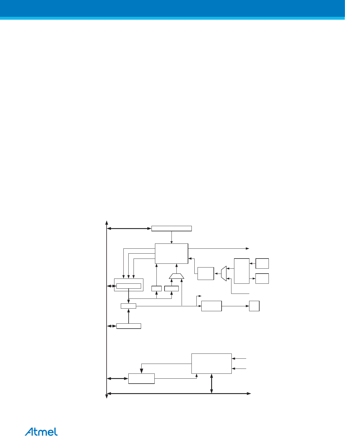
22. 8-bit Timer/Counter2 with PWM and Asynchronous Operation
22.1. Features
• Single Channel Counter
• Clear Timer on Compare Match (Auto Reload)
• Glitch-free, phase Correct Pulse Width Modulator (PWM)
• Frequency Generator
• 10-bit Clock Prescaler
• Overflow and Compare Match Interrupt Sources (TOV2 and OCF2)
• Allows Clocking from External 32kHz Watch Crystal Independent of the I/O Clock
22.2. Overview
Timer/Counter2 is a general purpose, single channel, 8-bit Timer/Counter module. A simplified block
diagram of the 8-bit Timer/Counter is shown in the figure below. For the actual placement of I/O pins, refer
to Pin Configurations. CPU accessible I/O Registers, including I/O bits and I/O pins, are shown in bold.
The device-specific I/O Register and bit locations are listed in the Register Description on page 160.
Figure 22-1 8-bit Timer/Counter Block Diagram
Timer/Counte r
DATA BUS
=
TCNTn
Waveform
Gene ra tion OCn
= 0
Control Logic
= 0xFF
TOPBOTTOM
count
clea r
direction
TOVn
(Int. Req.)
OCn
(Int. Req.)
Synchro nization Unit
OCRn
TCCRn
ASS Rn
Sta tus Flags
clkI/O
clkAS Y
Synchronize d Sta tus Fla gs
asynchronous Mode
Se le ct (ASn)
TOSC1
T/C
Oscillator
TOSC2
Pre sca ler
clkTn
clkI/O
Related Links
Pin Configurations on page 13
Atmel ATmega8A [DATASHEET]
Atmel-8159F-8-bit AVR Microcontroller_Datasheet_Complete-09/2015
147

22.2.1. Registers
The Timer/Counter (TCNT2) and Output Compare Register (OCR2) are 8-bit registers. Interrupt request
(shorten as Int.Req.) signals are all visible in the Timer Interrupt Flag Register (TIFR). All interrupts are
individually masked with the Timer Interrupt Mask Register (TIMSK). TIFR and TIMSK are not shown in
the figure since these registers are shared by other timer units.
The Timer/Counter can be clocked internally, via the prescaler, or asynchronously clocked from the
TOSC1/2 pins, as detailed later in this section. The asynchronous operation is controlled by the
Asynchronous Status Register (ASSR). The Clock Select logic block controls which clock source the
Timer/Counter uses to increment (or decrement) its value. The Timer/Counter is inactive when no clock
source is selected. The output from the clock select logic is referred to as the timer clock (clkT2).
The double buffered Output Compare Register (OCR2) is compared with the Timer/Counter value at all
times. The result of the compare can be used by the waveform generator to generate a PWM or variable
frequency output on the Output Compare Pin (OC2). For details, see Output Compare Unit. The Compare
Match event will also set the Compare Flag (OCF2) which can be used to generate an Output Compare
interrupt request.
22.2.2. Definitions
Many register and bit references in this document are written in general form. A lower case “n” replaces
the Timer/Counter number, in this case 2. However, when using the register or bit defines in a program,
the precise form must be used (i.e., TCNT2 for accessing Timer/Counter2 counter value and so on).
The definitions in the following table are also used extensively throughout the document.
Table 22-1 Definitions
BOTTOM The counter reaches the BOTTOM when it becomes zero (0x00).
MAX The counter reaches its MAXimum when it becomes 0xFF (decimal 255).
TOP The counter reaches the TOP when it becomes equal to the highest value in the
count sequence. The TOP value can be assigned to be the fixed value 0xFF (MAX)
or the value stored in the OCR2 Register. The assignment is dependent on the
mode of operation.
22.3. Timer/Counter Clock Sources
The Timer/Counter can be clocked by an internal synchronous or an external asynchronous clock source.
The clock source clkT2 is by default equal to the MCU clock, clkI/O. When the AS2 bit in the ASSR
Register is written to logic one, the clock source is taken from the Timer/Counter Oscillator connected to
TOSC1 and TOSC2. For details on asynchronous operation, refer to Asynchronous Operation of the
Timer/Counter on page 158. For details on clock sources and prescaler, refer to Timer/Counter Prescaler
on page 159.
Related Links
Timer/Counter0 and Timer/Counter1 Prescalers on page 108
22.4. Counter Unit
The main part of the 8-bit Timer/Counter is the programmable bi-directional counter unit. The following
figure shows a block diagram of the counter and its surrounding environment.
Atmel ATmega8A [DATASHEET]
Atmel-8159F-8-bit AVR Microcontroller_Datasheet_Complete-09/2015
148
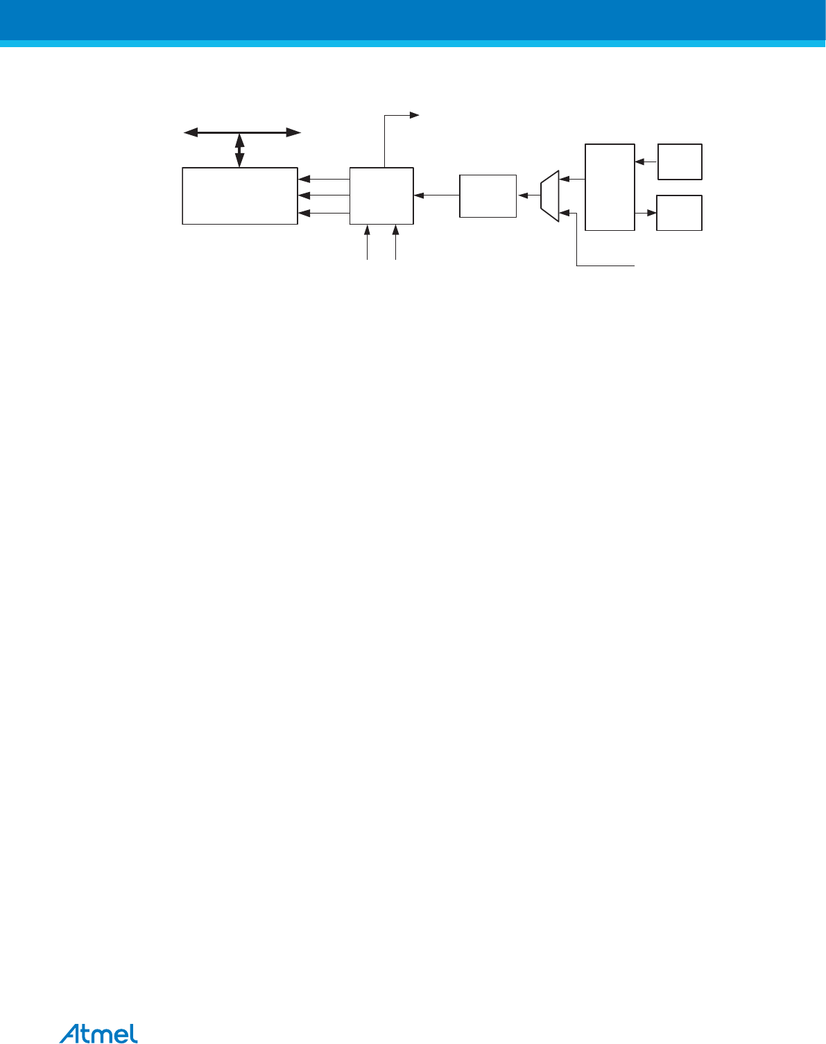
Figure 22-2 Counter Unit Block Diagram
DATA BUS
TCNTn Control Logic
count
TOVn
(Int. Req.)
TOPBOTTOM
direction
clear
TOS C1
T/C
Oscillator
TOS C2
Pres ca le r
clkI/O
clk Tn
Signal description (internal signals):
count Increment or decrement TCNT2 by 1.
direction Selects between increment and decrement.
clear Clear TCNT2 (set all bits to zero).
clkT2 Timer/Counter clock.
TOP Signalizes that TCNT2 has reached maximum value.
BOTTOM Signalizes that TCNT2 has reached minimum value (zero).
Depending on the mode of operation used, the counter is cleared, incremented, or decremented at each
timer clock (clkT2). clkT2 can be generated from an external or internal clock source, selected by the clock
select bits (CS22:0). When no clock source is selected (CS22:0 = 0) the timer is stopped. However, the
TCNT2 value can be accessed by the CPU, regardless of whether clkT2 is present or not. A CPU write
overrides (has priority over) all counter clear or count operations.
The counting sequence is determined by the setting of the WGM21 and WGM20 bits located in the Timer/
Counter Control Register (TCCR2). There are close connections between how the counter behaves
(counts) and how waveforms are generated on the Output Compare Output OC2. For more details about
advanced counting sequences and waveform generation, refer to Modes of Operation on page 152 .
The Timer/Counter Overflow (TOV2) Flag is set according to the mode of operation selected by the
WGM21:0 bits. TOV2 can be used for generating a CPU interrupt.
22.5. Output Compare Unit
The 8-bit comparator continuously compares TCNT2 with the Output Compare Register (OCR2).
Whenever TCNT2 equals OCR2, the comparator signals a match. A match will set the Output Compare
Flag (OCF2) at the next timer clock cycle. If enabled (OCIE2 = 1), the Output Compare Flag generates an
Output Compare interrupt. The OCF2 Flag is automatically cleared when the interrupt is executed.
Alternatively, the OCF2 Flag can be cleared by software by writing a logical one to its I/O bit location. The
waveform generator uses the match signal to generate an output according to operating mode set by the
WGM21:0 bits and Compare Output mode (COM21:0) bits. The max and bottom signals are used by the
waveform generator for handling the special cases of the extreme values in some modes of operation
(refer to Modes of Operation on page 152).
The following figure shows a block diagram of the Output Compare unit.
Atmel ATmega8A [DATASHEET]
Atmel-8159F-8-bit AVR Microcontroller_Datasheet_Complete-09/2015
149
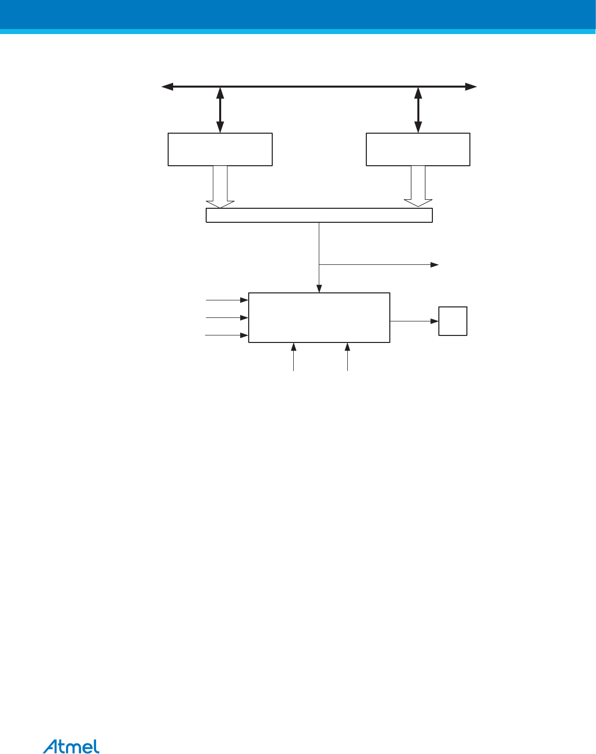
Figure 22-3 Output Compare Unit, Block Diagram
OCFn (Int. Re q.)
=(8-bit Comparator )
OCRn
OCxy
DATA BUS
TCNTn
WGMn1:0
Waveform Ge nerator
TOP
FOCn
COMn1:0
BOTTOM
The OCR2 Register is double buffered when using any of the Pulse Width Modulation (PWM) modes. For
the normal and Clear Timer on Compare (CTC) modes of operation, the double buffering is disabled. The
double buffering synchronizes the update of the OCR2 Compare Register to either top or bottom of the
counting sequence. The synchronization prevents the occurrence of odd-length, non-symmetrical PWM
pulses, thereby making the output glitch-free.
The OCR2 Register access may seem complex, but this is not case. When the double buffering is
enabled, the CPU has access to the OCR2 Buffer Register, and if double buffering is disabled the CPU
will access the OCR2 directly.
22.5.1. Force Output Compare
In non-PWM Waveform Generation modes, the match output of the comparator can be forced by writing a
one to the Force Output Compare (FOC2) bit. Forcing Compare Match will not set the OCF2 Flag or
reload/clear the timer, but the OC2 pin will be updated as if a real Compare Match had occurred (the
COM21:0 bits settings define whether the OC2 pin is set, cleared or toggled).
22.5.2. Compare Match Blocking by TCNT2 Write
All CPU write operations to the TCNT2 Register will block any Compare Match that occurs in the next
timer clock cycle, even when the timer is stopped. This feature allows OCR2 to be initialized to the same
value as TCNT2 without triggering an interrupt when the Timer/Counter clock is enabled.
22.5.3. Using the Output Compare Unit
Since writing TCNT2 in any mode of operation will block all compare matches for one timer clock cycle,
there are risks involved when changing TCNT2 when using the Output Compare channel, independently
of whether the Timer/Counter is running or not. If the value written to TCNT2 equals the OCR2 value, the
Atmel ATmega8A [DATASHEET]
Atmel-8159F-8-bit AVR Microcontroller_Datasheet_Complete-09/2015
150
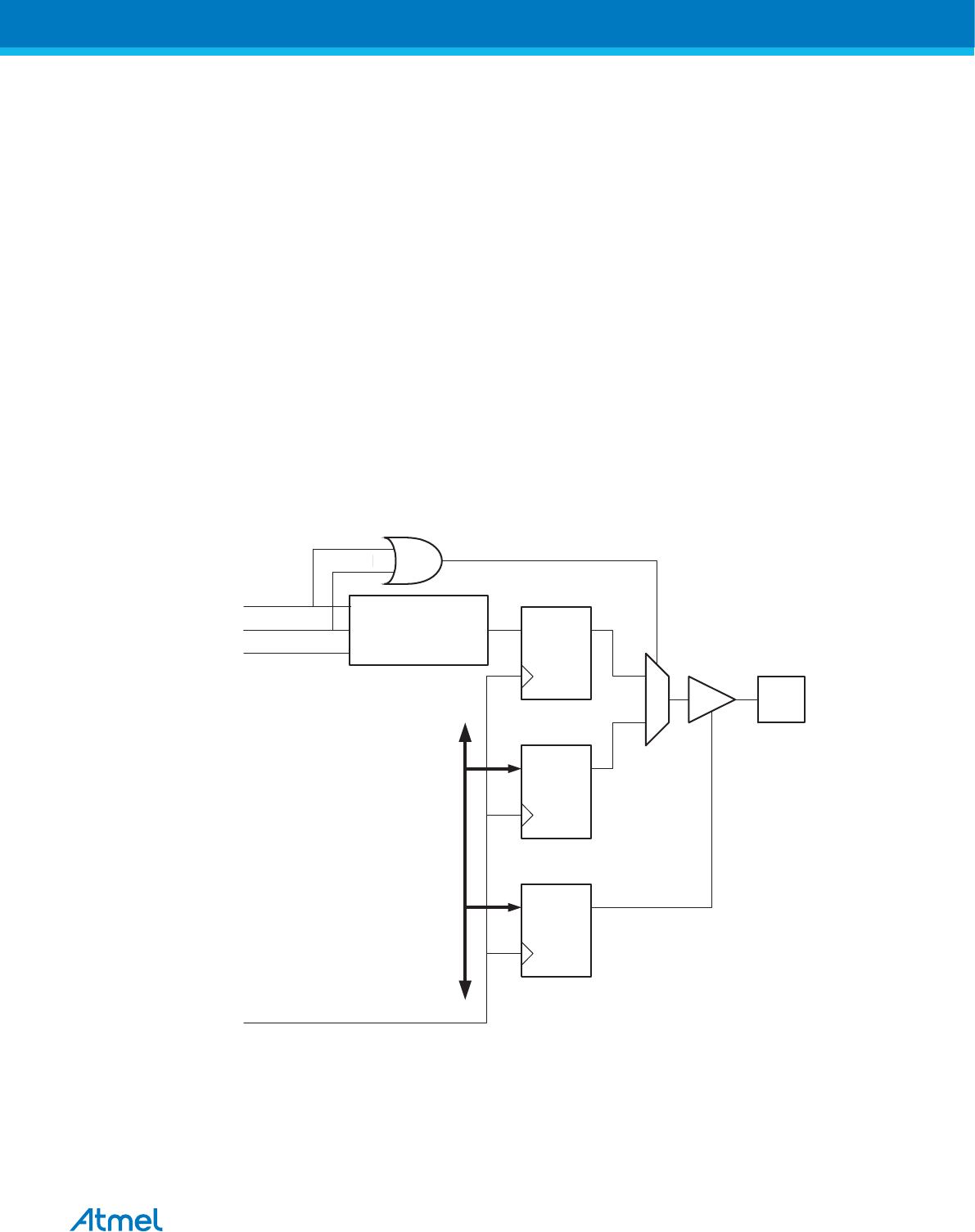
Compare Match will be missed, resulting in incorrect waveform generation. Similarly, do not write the
TCNT2 value equal to BOTTOM when the counter is downcounting.
The setup of the OC2 should be performed before setting the Data Direction Register for the port pin to
output. The easiest way of setting the OC2 value is to use the Force Output Compare (FOC2) strobe bit
in Normal mode. The OC2 Register keeps its value even when changing between waveform generation
modes.
Be aware that the COM21:0 bits are not double buffered together with the compare value. Changing the
COM21:0 bits will take effect immediately.
22.6. Compare Match Output Unit
The Compare Output mode (COM21:0) bits have two functions. The waveform generator uses the
COM21:0 bits for defining the Output Compare (OC2) state at the next Compare Match. Also, the
COM21:0 bits control the OC2 pin output source. The figure below shows a simplified schematic of the
logic affected by the COM21:0 bit setting. The I/O Registers, I/O bits, and I/O pins in the figure are shown
in bold. Only the parts of the general I/O Port Control Registers (DDR and PORT) that are affected by the
COM21:0 bits are shown. When referring to the OC2 state, the reference is for the internal OC2 Register,
not the OC2 pin.
Figure 22-4 Compare Match Output Unit, Schematic
PORT
DDR
D Q
D Q
OCn
Pin
OCn
D Q
Waveform
Gene rator
COMn1
COMn0
0
1
DATABUS
FOCn
clkI/O
The general I/O port function is overridden by the Output Compare (OC2) from the waveform generator if
either of the COM21:0 bits are set. However, the OC2 pin direction (input or output) is still controlled by
the Data Direction Register (DDR) for the port pin. The Data Direction Register bit for the OC2 pin
(DDR_OC2) must be set as output before the OC2 value is visible on the pin. The port override function is
independent of the Waveform Generation mode.
Atmel ATmega8A [DATASHEET]
Atmel-8159F-8-bit AVR Microcontroller_Datasheet_Complete-09/2015
151

The design of the Output Compare Pin logic allows initialization of the OC2 state before the output is
enabled. Note that some COM21:0 bit settings are reserved for certain modes of operation. See Register
Description.
22.6.1. Compare Output Mode and Waveform Generation
The Waveform Generator uses the COM21:0 bits differently in normal, CTC, and PWM modes. For all
modes, setting the COM21:0 = 0 tells the waveform generator that no action on the OC2 Register is to be
performed on the next Compare Match. For compare output actions in the non-PWM modes refer to table
Compare Output Mode, Non-PWM Mode. For fast PWM mode, refer to table Compare Output Mode, Fast
PWM Mode, and for phase correct PWM refer to table Compare Output Mode, Phase Correct PWM
Mode.
A change of the COM21:0 bits state will have effect at the first Compare Match after the bits are written.
For non-PWM modes, the action can be forced to have immediate effect by using the FOC2 strobe bits.
22.7. Modes of Operation
The mode of operation (i.e., the behavior of the Timer/Counter and the Output Compare pins) is defined
by the combination of the Waveform Generation mode (WGM21:0) and Compare Output mode
(COM21:0) bits. The Compare Output mode bits do not affect the counting sequence, while the Waveform
Generation mode bits do. The COM21:0 bits control whether the PWM output generated should be
inverted or not (inverted or non-inverted PWM). For non-PWM modes the COM21:0 bits control whether
the output should be set, cleared, or toggled at a Compare Match (refer to Compare Match Output Unit on
page 151).
For detailed timing information refer to Timer/Counter Timing Diagrams on page 156.
22.7.1. Normal Mode
The simplest mode of operation is the Normal mode (WGM21:0 = 0). In this mode the counting direction
is always up (incrementing), and no counter clear is performed. The counter simply overruns when it
passes its maximum 8-bit value (TOP = 0xFF) and then restarts from the bottom (0x00). In normal
operation the Timer/Counter Overflow Flag (TOV2) will be set in the same timer clock cycle as the TCNT2
becomes zero. The TOV2 Flag in this case behaves like a ninth bit, except that it is only set, not cleared.
However, combined with the timer overflow interrupt that automatically clears the TOV2 Flag, the timer
resolution can be increased by software. There are no special cases to consider in the Normal mode, a
new counter value can be written anytime.
The Output Compare unit can be used to generate interrupts at some given time. Using the Output
Compare to generate waveforms in Normal mode is not recommended, since this will occupy too much of
the CPU time.
22.7.2. Clear Timer on Compare Match (CTC) Mode
In Clear Timer on Compare or CTC mode (WGM21:0 = 2), the OCR2 Register is used to manipulate the
counter resolution. In CTC mode the counter is cleared to zero when the counter value (TCNT2) matches
the OCR2. The OCR2 defines the top value for the counter, hence also its resolution. This mode allows
greater control of the Compare Match output frequency. It also simplifies the operation of counting
external events.
The timing diagram for the CTC mode is shown in the figure below. The counter value (TCNT2) increases
until a Compare Match occurs between TCNT2 and OCR2, and then counter (TCNT2) is cleared.
Atmel ATmega8A [DATASHEET]
Atmel-8159F-8-bit AVR Microcontroller_Datasheet_Complete-09/2015
152
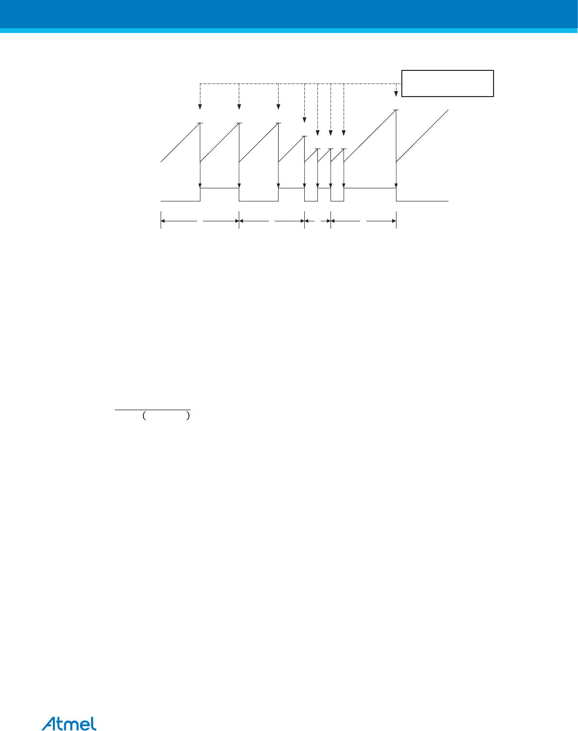
Figure 22-5 CTC Mode, Timing Diagram
TCNTn
OCn
(Toggle)
OCn Inte rrupt Flag Se t
1 4
Pe riod 2 3
(COMn1:0 = 1)
An interrupt can be generated each time the counter value reaches the TOP value by using the OCF2
Flag. If the interrupt is enabled, the interrupt handler routine can be used for updating the TOP value.
However, changing the TOP to a value close to BOTTOM when the counter is running with none or a low
prescaler value must be done with care since the CTC mode does not have the double buffering feature.
If the new value written to OCR2 is lower than the current value of TCNT2, the counter will miss the
Compare Match. The counter will then have to count to its maximum value (0xFF) and wrap around
starting at 0x00 before the Compare Match can occur.
For generating a waveform output in CTC mode, the OC2 output can be set to toggle its logical level on
each Compare Match by setting the Compare Output mode bits to toggle mode (COM21:0 = 1). The OC2
value will not be visible on the port pin unless the data direction for the pin is set to output. The waveform
generated will have a maximum frequency of fOC2 = fclk_I/O/2 when OCR2 is set to zero (0x00). The
waveform frequency is defined by the following equation:
OCn =clk_I/O
2 1 + OCRn
The N variable represents the prescaler factor (1, 8, 32, 64, 128, 256, or 1024).
As for the Normal mode of operation, the TOV2 Flag is set in the same timer clock cycle that the counter
counts from MAX to 0x00.
22.7.3. Fast PWM Mode
The fast Pulse Width Modulation or fast PWM mode (WGM21:0 = 3) provides a high frequency PWM
waveform generation option. The fast PWM differs from the other PWM option by its single-slope
operation. The counter counts from BOTTOM to MAX then restarts from BOTTOM. In non-inverting
Compare Output mode, the Output Compare (OC2) is cleared on the Compare Match between TCNT2
and OCR2, and set at BOTTOM. In inverting Compare Output mode, the output is set on Compare Match
and cleared at BOTTOM. Due to the single-slope operation, the operating frequency of the fast PWM
mode can be twice as high as the phase correct PWM mode that uses dual-slope operation. This high
frequency makes the fast PWM mode well suited for power regulation, rectification, and DAC
applications. High frequency allows physically small sized external components (coils, capacitors), and
therefore reduces total system cost.
In fast PWM mode, the counter is incremented until the counter value matches the MAX value. The
counter is then cleared at the following timer clock cycle. The timing diagram for the fast PWM mode is
shown in the following figure. The TCNT2 value is in the timing diagram shown as a histogram for
illustrating the single-slope operation. The diagram includes non-inverted and inverted PWM outputs. The
Atmel ATmega8A [DATASHEET]
Atmel-8159F-8-bit AVR Microcontroller_Datasheet_Complete-09/2015
153
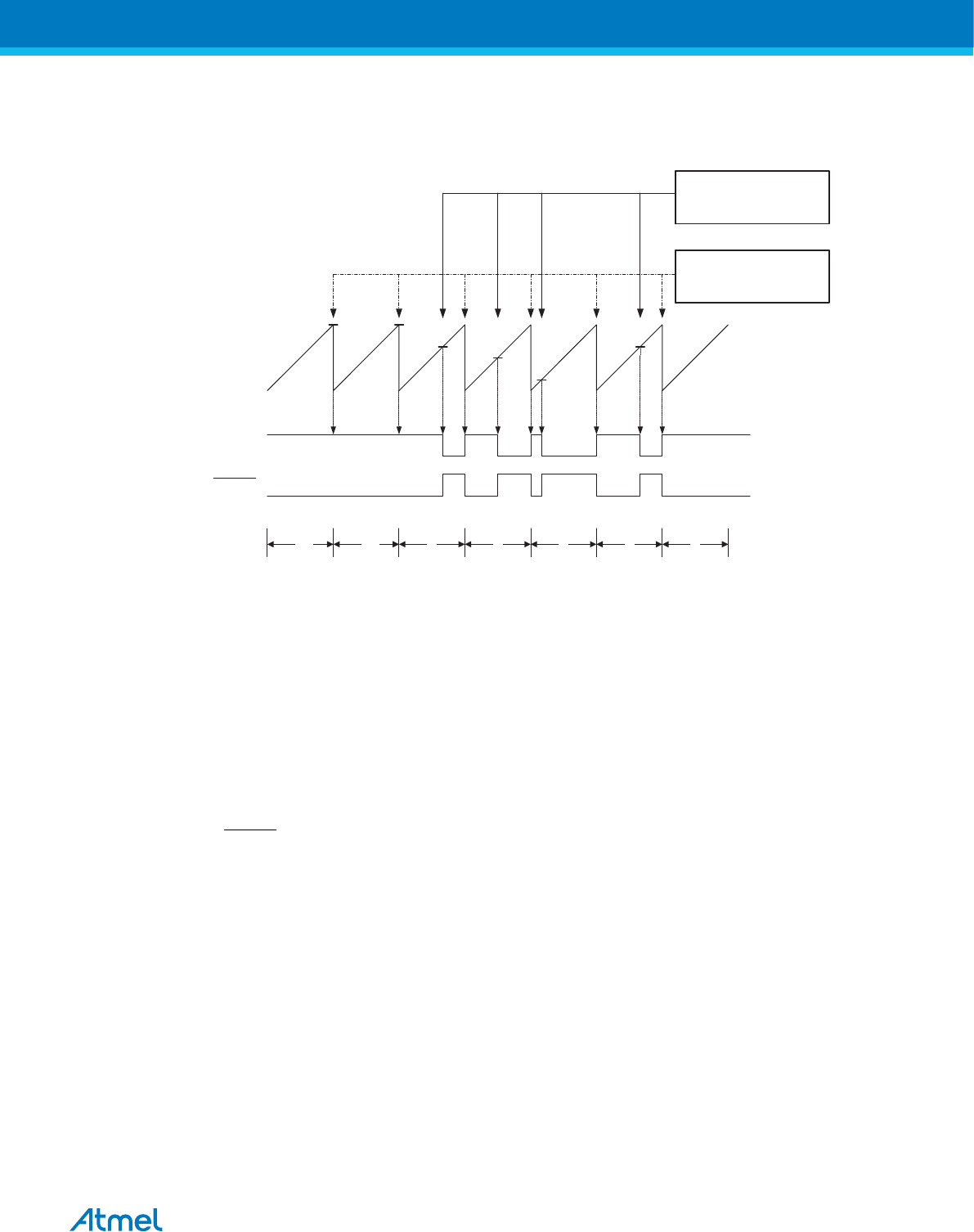
small horizontal line marks on the TCNT2 slopes represent compare matches between OCR2 and
TCNT2.
Figure 22-6 Fast PWM Mode, Timing Diagram
TCNTn
OCRn Upda te
and
TOVn Interrupt Fla g Se t
1
Pe riod 2 3
OCn
OCn
(COMn1:0 = 2)
(COMn1:0 = 3)
OCRn Inte rrupt Flag Se t
4 5 6 7
The Timer/Counter Overflow Flag (TOV2) is set each time the counter reaches MAX. If the interrupt is
enabled, the interrupt handler routine can be used for updating the compare value.
In fast PWM mode, the compare unit allows generation of PWM waveforms on the OC2 pin. Setting the
COM21:0 bits to 2 will produce a non-inverted PWM and an inverted PWM output can be generated by
setting the COM21:0 to 3 (refer to Table 22-4 Compare Output Mode, Fast PWM Mode(1) on page 162).
The actual OC2 value will only be visible on the port pin if the data direction for the port pin is set as
output. The PWM waveform is generated by setting (or clearing) the OC2 Register at the Compare Match
between OCR2 and TCNT2, and clearing (or setting) the OC2 Register at the timer clock cycle the
counter is cleared (changes from MAX to BOTTOM).
The PWM frequency for the output can be calculated by the following equation:
OCnPWM =clk_I/O
256
The N variable represents the prescaler factor (1, 8, 32, 64, 128, 256, or 1024).
The extreme values for the OCR2 Register represent special cases when generating a PWM waveform
output in the fast PWM mode. If the OCR2 is set equal to BOTTOM, the output will be a narrow spike for
each MAX+1 timer clock cycle. Setting the OCR2 equal to MAX will result in a constantly high or low
output (depending on the polarity of the output set by the COM21:0 bits.)
A frequency (with 50% duty cycle) waveform output in fast PWM mode can be achieved by setting OC2 to
toggle its logical level on each Compare Match (COM21:0 = 1). The waveform generated will have a
maximum frequency of foc2 = fclk_I/O/2 when OCR2 is set to zero. This feature is similar to the OC2 toggle
in CTC mode, except the double buffer feature of the Output Compare unit is enabled in the fast PWM
mode.
22.7.4. Phase Correct PWM Mode
The phase correct PWM mode (WGM21:0 = 1) provides a high resolution phase correct PWM waveform
generation option. The phase correct PWM mode is based on a dual-slope operation. The counter counts
Atmel ATmega8A [DATASHEET]
Atmel-8159F-8-bit AVR Microcontroller_Datasheet_Complete-09/2015
154
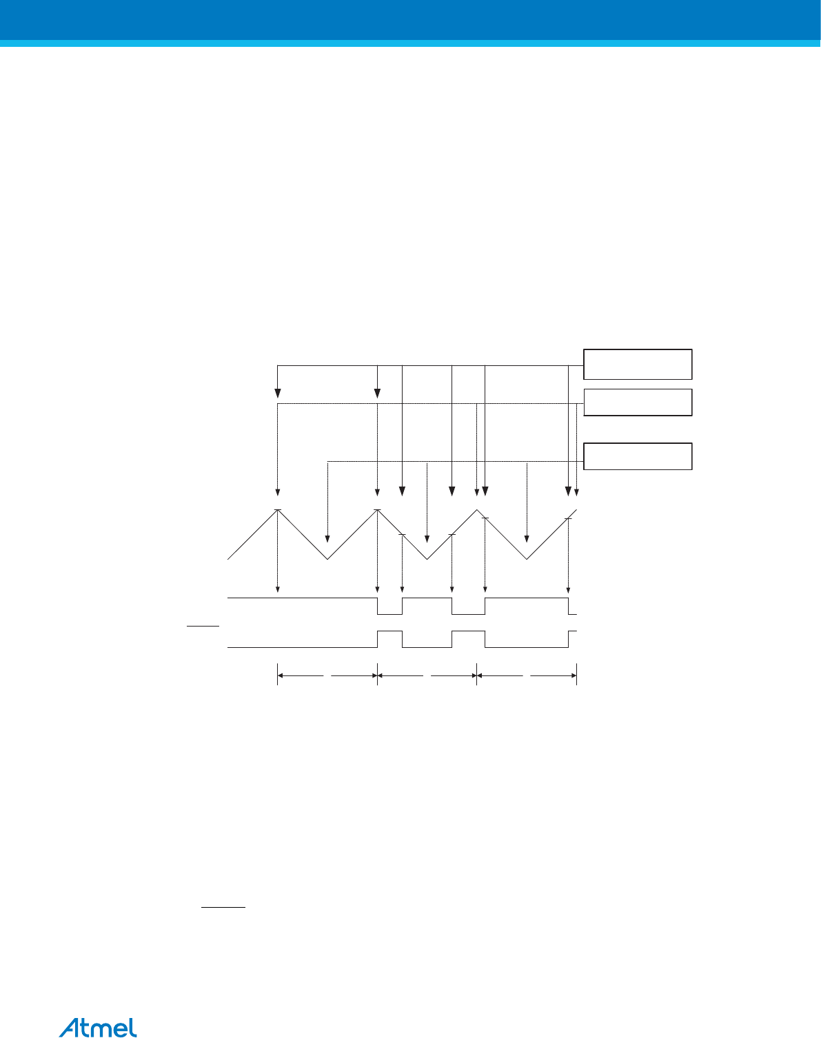
repeatedly from BOTTOM to MAX and then from MAX to BOTTOM. In non-inverting Compare Output
mode, the Output Compare (OC2) is cleared on the Compare Match between TCNT2 and OCR2 while
upcounting, and set on the Compare Match while downcounting. In inverting Output Compare mode, the
operation is inverted. The dual-slope operation has lower maximum operation frequency than single slope
operation. However, due to the symmetric feature of the dual-slope PWM modes, these modes are
preferred for motor control applications.
The PWM resolution for the phase correct PWM mode is fixed to eight bits. In phase correct PWM mode
the counter is incremented until the counter value matches MAX. When the counter reaches MAX, it
changes the count direction. The TCNT2 value will be equal to MAX for one timer clock cycle. The timing
diagram for the phase correct PWM mode is shown on the following figure. The TCNT2 value is in the
timing diagram shown as a histogram for illustrating the dual-slope operation. The diagram includes non-
inverted and inverted PWM outputs. The small horizontal line marks on the TCNT2 slopes represent
compare matches between OCR2 and TCNT2.
Figure 22-7 Phase Correct PWM Mode, Timing Diagram
TOVn Interrupt Flag S e t
OCn Interrupt Flag S e t
1 2 3
TCNTn
Pe riod
OCn
OCn
(COMn1:0 = 2)
(COMn1:0 = 3)
OCRn Update
The Timer/Counter Overflow Flag (TOV2) is set each time the counter reaches BOTTOM. The Interrupt
Flag can be used to generate an interrupt each time the counter reaches the BOTTOM value.
In phase correct PWM mode, the compare unit allows generation of PWM waveforms on the OC2 pin.
Setting the COM21:0 bits to 2 will produce a non-inverted PWM. An inverted PWM output can be
generated by setting the COM21:0 to 3 (refer to table Compare Output Mode, Phase Correct PWM
Mode). The actual OC2 value will only be visible on the port pin if the data direction for the port pin is set
as output. The PWM waveform is generated by clearing (or setting) the OC2 Register at the Compare
Match between OCR2 and TCNT2 when the counter increments, and setting (or clearing) the OC2
Register at Compare Match between OCR2 and TCNT2 when the counter decrements. The PWM
frequency for the output when using phase correct PWM can be calculated by the following equation:
OCnPCPWM =clk_I/O
510
The N variable represents the prescaler factor (1, 8, 32, 64, 128, 256, or 1024).
Atmel ATmega8A [DATASHEET]
Atmel-8159F-8-bit AVR Microcontroller_Datasheet_Complete-09/2015
155
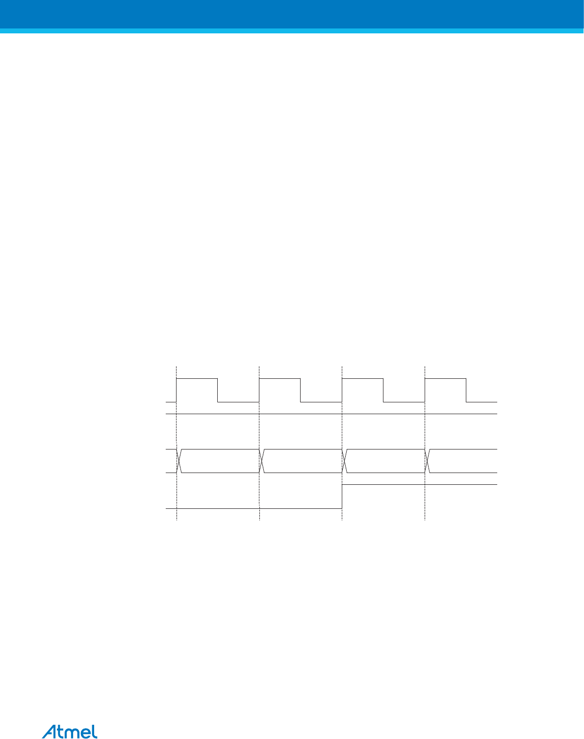
The extreme values for the OCR2 Register represent special cases when generating a PWM waveform
output in the phase correct PWM mode. If the OCR2 is set equal to BOTTOM, the output will be
continuously low and if set equal to MAX the output will be continuously high for non-inverted PWM
mode. For inverted PWM the output will have the opposite logic values.
At the very start of period 2 in the timing diagram above OCn has a transition from high to low even
though there is no Compare Match. The point of this transition is to guarantee symmetry around
BOTTOM. There are two cases that give a transition without Compare Match:
• OCR2A changes its value from MAX, like in the timing diagram above. When the OCR2A value is MAX
the OCn pin value is the same as the result of a down-counting Compare Match. To ensure symmetry
around BOTTOM the OCn value at MAX must correspond to the result of an up-counting Compare
Match.
• The timer starts counting from a value higher than the one in OCR2A, and for that reason misses the
Compare Match and hence the OCn change that would have happened on the way up.
22.8. Timer/Counter Timing Diagrams
The following figures show the Timer/Counter in Synchronous mode, and the timer clock (clkT2) is
therefore shown as a clock enable signal. In Asynchronous mode, clkI/O should be replaced by the Timer/
Counter Oscillator clock. The figures include information on when Interrupt Flags are set. The following
figure contains timing data for basic Timer/Counter operation. The figure shows the count sequence close
to the MAX value in all modes other than phase correct PWM mode.
Figure 22-8 Timer/Counter Timing Diagram, no Prescaling
clkTn
(clkI/O/1)
TOVn
clkI/O
TCNTn MAX - 1 MAX BOTTOM BOTTOM + 1
The next figure shows the same timing data, but with the prescaler enabled.
Atmel ATmega8A [DATASHEET]
Atmel-8159F-8-bit AVR Microcontroller_Datasheet_Complete-09/2015
156
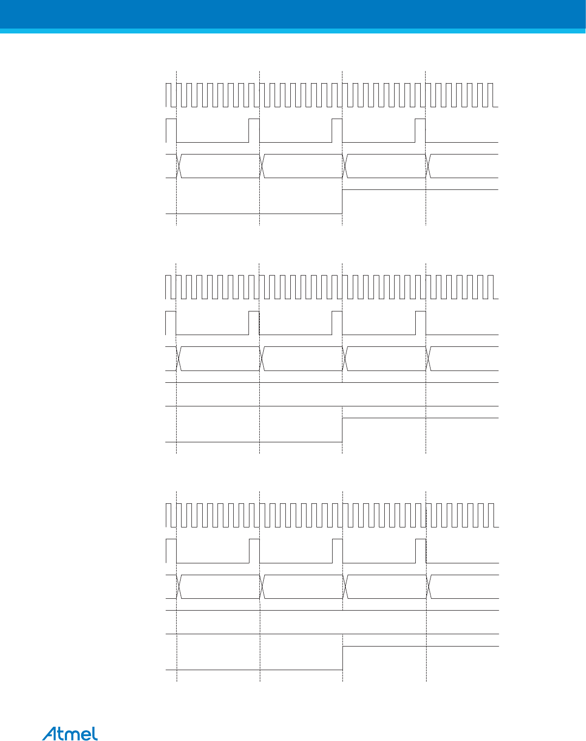
Figure 22-9 Timer/Counter Timing Diagram, with Prescaler (fclk_I/O/8)
TOVn
TCNTn MAX - 1 MAX BOTTOM BOTTOM + 1
clkI/O
clkTn
(clkI/O/8)
The next figure shows the setting of OCF2 in all modes except CTC mode.
Figure 22-10 Timer/Counter Timing Diagram, Setting of OCF2, with Prescaler (fclk_I/O/8)
OCFn
OCRn
TCNTn
OCRn Value
OCRn - 1 OCRn OCRn + 1 OCRn + 2
clkI/O
clkTn
(clkI/O/8)
The figure below shows the setting of OCF2 and the clearing of TCNT2 in CTC mode.
Figure 22-11 Timer/Counter Timing Diagram, Clear Timer on Compare Match Mode, with Prescaler (fclk_I/O/8)
OCFn
OCRn
TCNTn
(CTC)
TOP
TOP - 1 TOP BOTTOM BOTTOM + 1
clkI/O
clkTn
(clkI/O/8)
Atmel ATmega8A [DATASHEET]
Atmel-8159F-8-bit AVR Microcontroller_Datasheet_Complete-09/2015
157

22.9. Asynchronous Operation of the Timer/Counter
22.9.1. Asynchronous Operation of Timer/Counter2
When Timer/Counter2 operates asynchronously, some considerations must be taken.
•Warning: When switching between asynchronous and synchronous clocking of Timer/Counter2, the
Timer Registers TCNT2, OCR2, and TCCR2 might be corrupted. A safe procedure for switching
clock source is:
1. Disable the Timer/Counter2 interrupts by clearing OCIE2 and TOIE2.
2. Select clock source by setting AS2 as appropriate.
3. Write new values to TCNT2, OCR2, and TCCR2.
4. To switch to asynchronous operation: Wait for TCN2UB, OCR2UB, and TCR2UB.
5. Clear the Timer/Counter2 Interrupt Flags.
6. Enable interrupts, if needed.
•The Oscillator is optimized for use with a 32.768kHz watch crystal. Applying an external clock to the
TOSC1 pin may result in incorrect Timer/Counter2 operation. The CPU main clock frequency must
be more than four times the Oscillator frequency.
•When writing to one of the registers TCNT2, OCR2, or TCCR2, the value is transferred to a
temporary register, and latched after two positive edges on TOSC1. The user should not write a
new value before the contents of the temporary register have been transferred to its destination.
Each of the three mentioned registers have their individual temporary register, which means that
e.g. writing to TCNT2 does not disturb an OCR2 write in progress. To detect that a transfer to the
destination register has taken place, the Asynchronous Status Register – ASSR has been
implemented.
•When entering Power-save mode after having written to TCNT2, OCR2, or TCCR2, the user must
wait until the written register has been updated if Timer/Counter2 is used to wake up the device.
Otherwise, the MCU will enter sleep mode before the changes are effective. This is particularly
important if the Output Compare2 interrupt is used to wake up the device, since the Output
Compare function is disabled during writing to OCR2 or TCNT2. If the write cycle is not finished,
and the MCU enters sleep mode before the OCR2UB bit returns to zero, the device will never
receive a Compare Match interrupt, and the MCU will not wake up.
•If Timer/Counter2 is used to wake the device up from Power-save or Extended Standby mode,
precautions must be taken if the user wants to re-enter one of these modes: The interrupt logic
needs one TOSC1 cycle to be reset. If the time between wake-up and re-entering sleep mode is
less than one TOSC1 cycle, the interrupt will not occur, and the device will fail to wake up. If the
user is in doubt whether the time before re-entering Power-save or Extended Standby mode is
sufficient, the following algorithm can be used to ensure that one TOSC1 cycle has elapsed:
1. Write a value to TCCR2, TCNT2, or OCR2.
2. Wait until the corresponding Update Busy Flag in ASSR returns to zero.
3. Enter Power-save or Extended Standby mode.
•When the asynchronous operation is selected, the 32.768kHz Oscillator for Timer/Counter2 is
always running, except in Power-down and Standby modes. After a Power-up Reset or Wake-up
from Power-down or Standby mode, the user should be aware of the fact that this Oscillator might
take as long as one second to stabilize. The user is advised to wait for at least one second before
using Timer/Counter2 after Power-up or Wake-up from Power-down or Standby mode. The
contents of all Timer/Counter2 Registers must be considered lost after a wake-up from Power-down
Atmel ATmega8A [DATASHEET]
Atmel-8159F-8-bit AVR Microcontroller_Datasheet_Complete-09/2015
158
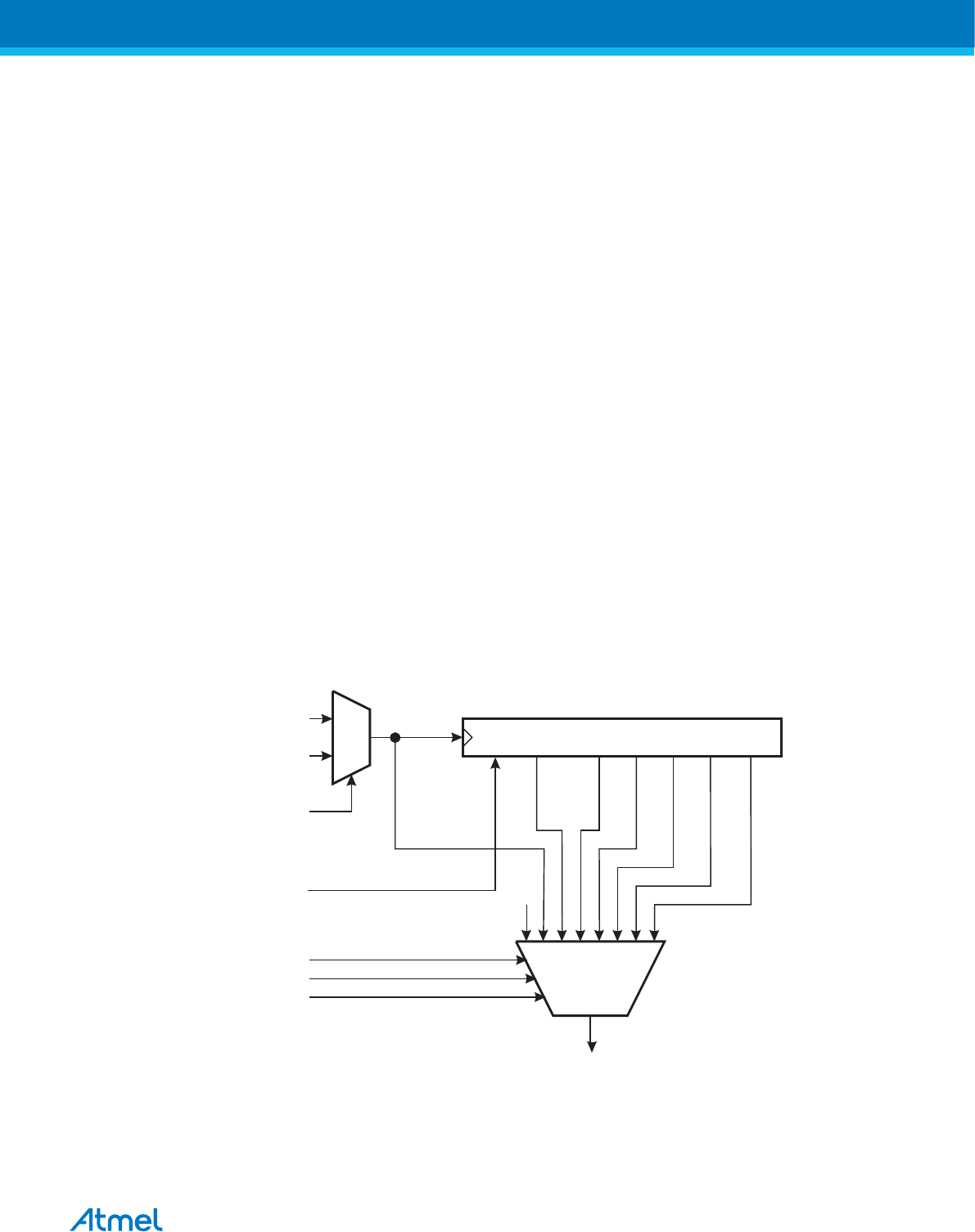
or Standby mode due to unstable clock signal upon start-up, no matter whether the Oscillator is in
use or a clock signal is applied to the TOSC1 pin.
•Description of wake up from Power-save or Extended Standby mode when the timer is clocked
asynchronously: When the interrupt condition is met, the wake up process is started on the
following cycle of the timer clock, that is, the timer is always advanced by at least one before the
processor can read the counter value. After wake-up, the MCU is halted for four cycles, it executes
the interrupt routine, and resumes execution from the instruction following SLEEP.
•Reading of the TCNT2 Register shortly after wake-up from Power-save may give an incorrect
result. Since TCNT2 is clocked on the asynchronous TOSC clock, reading TCNT2 must be done
through a register synchronized to the internal I/O clock domain. Synchronization takes place for
every rising TOSC1 edge. When waking up from Power-save mode, and the I/O clock (clkI/O) again
becomes active, TCNT2 will read as the previous value (before entering sleep) until the next rising
TOSC1 edge. The phase of the TOSC clock after waking up from Power-save mode is essentially
unpredictable, as it depends on the wake-up time. The recommended procedure for reading
TCNT2 is thus as follows:
1. Write any value to either of the registers OCR2 or TCCR2.
2. Wait for the corresponding Update Busy Flag to be cleared.
3. Read TCNT2.
•During asynchronous operation, the synchronization of the Interrupt Flags for the asynchronous
timer takes three processor cycles plus one timer cycle. The timer is therefore advanced by at least
one before the processor can read the timer value causing the setting of the Interrupt Flag. The
Output Compare Pin is changed on the timer clock and is not synchronized to the processor clock.
22.10. Timer/Counter Prescaler
Figure 22-12 Prescaler for Timer/Counter2
10-BIT T/C PRESCALER
TIMER/COUNTER2 CLOCK SOURCE
clkI/O clkT2S
TOS C1
AS2
CS 20
CS 21
CS 22
clkT2S
/8
clkT2S
/64
clkT2S
/128
clkT2S
/1024
clkT2S
/256
clkT2S
/32
0
PS R2
Clea r
clkT2
The clock source for Timer/Counter2 is named clkT2S. clkT2S is by default connected to the main system
clock clkI/O. By setting the AS2 bit in ASSR, Timer/Counter2 is asynchronously clocked from the TOSC1
pin. This enables use of Timer/Counter2 as a Real Time Counter (RTC). When AS2 is set, pins TOSC1
Atmel ATmega8A [DATASHEET]
Atmel-8159F-8-bit AVR Microcontroller_Datasheet_Complete-09/2015
159

and TOSC2 are disconnected from Port B. A crystal can then be connected between the TOSC1 and
TOSC2 pins to serve as an independent clock source for Timer/Counter2. The Oscillator is optimized for
use with a 32.768kHz crystal. Applying an external clock source to TOSC1 is not recommended.
For Timer/Counter2, the possible prescaled selections are: clkT2S/8, clkT2S/32, clkT2S/64, clkT2S/128,
clkT2S/256, and clkT2S/1024. Additionally, clkT2S as well as 0 (stop) may be selected. Setting the PSR2 bit
in SFIOR resets the prescaler. This allows the user to operate with a predictable prescaler.
22.11. Register Description
Atmel ATmega8A [DATASHEET]
Atmel-8159F-8-bit AVR Microcontroller_Datasheet_Complete-09/2015
160
22.11.1. TCCR2 – Timer/Counter Control Register
When using the I/O specific commands IN and OUT, the I/O addresses 0x00 - 0x3F must be used. When
addressing I/O Registers as data space using LD and ST instructions, 0x20 must be added to these offset
addresses. The device is a complex microcontroller with more peripheral units than can be supported
within the 64 location reserved in Opcode for the IN and OUT instructions. For the Extended I/O space
from 0x60 in SRAM, only the ST/STS/STD and LD/LDS/LDD instructions can be used.
Name: TCCR2
Offset: 0x25
Reset: 0x00
Property:
When addressing I/O Registers as data space the offset address is 0x45
Bit 7 6 5 4 3 2 1 0
FOC2 WGM20 COM21 COM20 WGM21 CS22 CS21 CS20
Access W R/W R/W R/W R/W R/W R/W R/W
Reset 0 0 0 0 0 0 0 0
Bit 7 – FOC2: Force Output Compare
The FOC2 bit is only active when the WGM bits specify a non-PWM mode. However, for ensuring
compatibility with future devices, this bit must be set to zero when TCCR2 is written when operating in
PWM mode. When writing a logical one to the FOC2 bit, an immediate Compare Match is forced on the
waveform generation unit. The OC2 output is changed according to its COM21:0 bits setting. Note that
the FOC2 bit is implemented as a strobe. Therefore it is the value present in the COM21:0 bits that
determines the effect of the forced compare.
A FOC2 strobe will not generate any interrupt, nor will it clear the timer in CTC mode using OCR2 as
TOP.
The FOC2 bit is always read as zero.
Bit 6 – WGM20: Waveform Generation Mode [n=0:1]
These bits control the counting sequence of the counter, the source for the maximum (TOP) counter
value, and what type of waveform generation to be used. Modes of operation supported by the Timer/
Counter unit are: Normal mode, Clear Timer on Compare Match (CTC) mode, and two types of Pulse
Width Modulation (PWM) modes. See table below and Modes of Operation.
Table 22-2 Waveform Generation Mode Bit Description
Mode WGM21
(CTC2)
WGM20
(PWM2)
Timer/Counter Mode of Operation(1) TOP Update of
OCR2
TOV2 Flag
Set
0 0 0 Normal 0xFF Immediate MAX
1 0 1 PWM, Phase Correct 0xFF TOP BOTTOM
2 1 0 CTC OCR2 Immediate MAX
3 1 1 Fast PWM 0xFF BOTTOM MAX
Note: 1. The CTC2 and PWM2 bit definition names are now obsolete. Use the WGM21:0 definitions.
However, the functionality and location of these bits are compatible with previous versions of the timer.
Atmel ATmega8A [DATASHEET]
Atmel-8159F-8-bit AVR Microcontroller_Datasheet_Complete-09/2015
161

Bits 5:4 – COM2n: Compare Match Output Mode [n = 1:0]
These bits control the Output Compare Pin (OC2) behavior. If one or both of the COM21:0 bits are set,
the OC2 output overrides the normal port functionality of the I/O pin it is connected to. However, note that
the Data Direction Register (DDR) bit corresponding to OC2 pin must be set in order to enable the output
driver.
When OC2 is connected to the pin, the function of the COM21:0 bits depends on the WGM21:0 bit
setting. The following table shows the COM21:0 bit functionality when the WGM21:0 bits are set to a
normal or CTC mode (non-PWM).
Table 22-3 Compare Output Mode, Non-PWM Mode
COM21 COM20 Description
0 0 Normal port operation, OC2 disconnected.
0 1 Toggle OC2 on Compare Match
1 0 Clear OC2 on Compare Match
1 1 Set OC2 on Compare Match
The next table shows the COM21:0 bit functionality when the WGM21:0 bits are set to fast PWM mode.
Table 22-4 Compare Output Mode, Fast PWM Mode(1)
COM21 COM20 Description
0 0 Normal port operation, OC2 disconnected.
0 1 Reserved
1 0 Clear OC2 on Compare Match, set OC2 at BOTTOM,
(non-inverting mode)
1 1 Set OC2 on Compare Match, clear OC2 at BOTTOM,
(inverting mode)
Note: 1. A special case occurs when OCR2 equals TOP and COM21 is set. In this case, the Compare
Match is ignored, but the set or clear is done at BOTTOM. See Fast PWM Mode for more details.
The table below shows the COM21:0 bit functionality when the WGM21:0 bits are set to phase correct
PWM mode.
Table 22-5 Compare Output Mode, Phase Correct PWM Mode(1)
COM21 COM20 Description
0 0 Normal port operation, OC2 disconnected.
0 1 Reserved
1 0 Clear OC2 on Compare Match when up-counting. Set OC2 on Compare Match when
downcounting.
1 1 Set OC2 on Compare Match when up-counting. Clear OC2 on Compare Match when
downcounting.
Note: 1. A special case occurs when OCR2 equals TOP and COM21 is set. In this case, the Compare
Match is ignored, but the set or clear is done at TOP. See Phase Correct PWM Mode for more details.
Atmel ATmega8A [DATASHEET]
Atmel-8159F-8-bit AVR Microcontroller_Datasheet_Complete-09/2015
162

Bit 3 – WGM21: Waveform Generation Mode [n=0:1]
Refer to WGM20.
Bits 2:0 – CS2n: Clock Select [n = 2:0]
The three Clock Select bits select the clock source to be used by the Timer/Counter.
Table 22-6 Clock Select Bit Description
CS22 CS21 CS20 Description
0 0 0 No clock source (Timer/Counter stopped).
0 0 1 clkI/O/1 (No prescaling)
0 1 0 clkI/O/8 (From prescaler)
0 1 1 clkI/O/32 (From prescaler)
1 0 0 clkI/O/64 (From prescaler)
1 0 1 clkI/O/128 (From prescaler)
1 1 0 clkI/O/256 (From prescaler)
1 1 1 clkI/O/1024 (From prescaler)
Atmel ATmega8A [DATASHEET]
Atmel-8159F-8-bit AVR Microcontroller_Datasheet_Complete-09/2015
163

22.11.2. TCNT2 – Timer/Counter Register
When using the I/O specific commands IN and OUT, the I/O addresses 0x00 - 0x3F must be used. When
addressing I/O Registers as data space using LD and ST instructions, 0x20 must be added to these offset
addresses. The device is a complex microcontroller with more peripheral units than can be supported
within the 64 location reserved in Opcode for the IN and OUT instructions. For the Extended I/O space
from 0x60 in SRAM, only the ST/STS/STD and LD/LDS/LDD instructions can be used.
The Timer/Counter Register gives direct access, both for read and write operations, to the Timer/Counter
unit 8-bit counter. Writing to the TCNT2 Register blocks (removes) the Compare Match on the following
timer clock. Modifying the counter (TCNT2) while the counter is running, introduces a risk of missing a
Compare Match between TCNT2 and the OCR2 Register.
Name: TCNT2
Offset: 0x24
Reset: 0x00
Property:
When addressing I/O Registers as data space the offset address is 0x44
Bit 7 6 5 4 3 2 1 0
TCNT2[7:0]
Access R/W R/W R/W R/W R/W R/W R/W R/W
Reset 0 0 0 0 0 0 0 0
Bits 7:0 – TCNT2[7:0]
Atmel ATmega8A [DATASHEET]
Atmel-8159F-8-bit AVR Microcontroller_Datasheet_Complete-09/2015
164

22.11.3. OCR2 – Output Compare Register
When using the I/O specific commands IN and OUT, the I/O addresses 0x00 - 0x3F must be used. When
addressing I/O Registers as data space using LD and ST instructions, 0x20 must be added to these offset
addresses. The device is a complex microcontroller with more peripheral units than can be supported
within the 64 location reserved in Opcode for the IN and OUT instructions. For the Extended I/O space
from 0x60 in SRAM, only the ST/STS/STD and LD/LDS/LDD instructions can be used.
The Output Compare Register contains an 8-bit value that is continuously compared with the counter
value (TCNT2). A match can be used to generate an Output Compare interrupt, or to generate a
waveform output on the OC2 pin.
Name: OCR2
Offset: 0x23
Reset: 0x00
Property:
When addressing I/O Registers as data space the offset address is 0x43
Bit 7 6 5 4 3 2 1 0
OCR2[7:0]
Access R/W R/W R/W R/W R/W R/W R/W R/W
Reset 0 0 0 0 0 0 0 0
Bits 7:0 – OCR2[7:0]
Atmel ATmega8A [DATASHEET]
Atmel-8159F-8-bit AVR Microcontroller_Datasheet_Complete-09/2015
165

22.11.4. ASSR – Asynchronous Status Register
When using the I/O specific commands IN and OUT, the I/O addresses 0x00 - 0x3F must be used. When
addressing I/O Registers as data space using LD and ST instructions, 0x20 must be added to these offset
addresses. The device is a complex microcontroller with more peripheral units than can be supported
within the 64 location reserved in Opcode for the IN and OUT instructions. For the Extended I/O space
from 0x60 in SRAM, only the ST/STS/STD and LD/LDS/LDD instructions can be used.
Name: ASSR
Offset: 0x22
Reset: 0x00
Property:
When addressing I/O Registers as data space the offset address is 0x42
Bit 7 6 5 4 3 2 1 0
AS2 TCN2UB OCR2UB TCR2UB
Access R/W R R R
Reset 0 0 0 0
Bit 3 – AS2: Asynchronous Timer/Counter2
When AS2 is written to zero, Timer/Counter 2 is clocked from the I/O clock, clkI/O. When AS2 is written to
one, Timer/Counter 2 is clocked from a crystal Oscillator connected to the Timer Oscillator 1 (TOSC1) pin.
When the value of AS2 is changed, the contents of TCNT2, OCR2, and TCCR2 might be corrupted.
Bit 2 – TCN2UB: Timer/Counter2 Update Busy
When Timer/Counter2 operates asynchronously and TCNT2 is written, this bit becomes set. When
TCNT2 has been updated from the temporary storage register, this bit is cleared by hardware. A logical
zero in this bit indicates that TCNT2 is ready to be updated with a new value.
Bit 1 – OCR2UB: Output Compare Register2 Update Busy
When Timer/Counter2 operates asynchronously and OCR2 is written, this bit becomes set. When OCR2
has been updated from the temporary storage register, this bit is cleared by hardware. A logical zero in
this bit indicates that OCR2 is ready to be updated with a new value.
Bit 0 – TCR2UB: Timer/Counter Control Register2 Update Busy
When Timer/Counter2 operates asynchronously and TCCR2 is written, this bit becomes set. When
TCCR2 has been updated from the temporary storage register, this bit is cleared by hardware. A logical
zero in this bit indicates that TCCR2 is ready to be updated with a new value.
If a write is performed to any of the three Timer/Counter2 Registers while its update busy flag is set, the
updated value might get corrupted and cause an unintentional interrupt to occur.
The mechanisms for reading TCNT2, OCR2, and TCCR2 are different. When reading TCNT2, the actual
timer value is read. When reading OCR2 or TCCR2, the value in the temporary storage register is read.
Atmel ATmega8A [DATASHEET]
Atmel-8159F-8-bit AVR Microcontroller_Datasheet_Complete-09/2015
166

22.11.5. TIMSK – Timer/Counter Interrupt Mask Register
When using the I/O specific commands IN and OUT, the I/O addresses 0x00 - 0x3F must be used. When
addressing I/O Registers as data space using LD and ST instructions, 0x20 must be added to these offset
addresses. The device is a complex microcontroller with more peripheral units than can be supported
within the 64 location reserved in Opcode for the IN and OUT instructions. For the Extended I/O space
from 0x60 in SRAM, only the ST/STS/STD and LD/LDS/LDD instructions can be used.
Name: TIMSK
Offset: 0x39
Reset: 0x00
Property:
When addressing I/O Registers as data space the offset address is 0x59
Bit 7 6 5 4 3 2 1 0
OCIE2 TOIE2
Access R/W R/W
Reset 0 0
Bit 7 – OCIE2: Timer/Counter2 Output Compare Match Interrupt Enable
When the OCIE2 bit is written to one and the I-bit in the Status Register is set (one), the Timer/Counter2
Compare Match interrupt is enabled. The corresponding interrupt is executed if a Compare Match in
Timer/Counter2 occurs (i.e., when the OCF2 bit is set in the Timer/Counter Interrupt Flag Register –
TIFR).
Bit 6 – TOIE2: Timer/Counter2 Overflow Interrupt Enable
When the TOIE2 bit is written to one and the I-bit in the Status Register is set (one), the Timer/Counter2
Overflow interrupt is enabled. The corresponding interrupt is executed if an overflow in Timer/Counter2
occurs (i.e., when the TOV2 bit is set in the Timer/Counter Interrupt Flag Register – TIFR).
Atmel ATmega8A [DATASHEET]
Atmel-8159F-8-bit AVR Microcontroller_Datasheet_Complete-09/2015
167

22.11.6. TIFR – Timer/Counter Interrupt Flag Register
When using the I/O specific commands IN and OUT, the I/O addresses 0x00 - 0x3F must be used. When
addressing I/O Registers as data space using LD and ST instructions, 0x20 must be added to these offset
addresses. The device is a complex microcontroller with more peripheral units than can be supported
within the 64 location reserved in Opcode for the IN and OUT instructions. For the Extended I/O space
from 0x60 in SRAM, only the ST/STS/STD and LD/LDS/LDD instructions can be used.
Name: TIFR
Offset: 0x38
Reset: 0x00
Property:
When addressing I/O Registers as data space the offset address is 0x58
Bit 7 6 5 4 3 2 1 0
OCF2 TOV2
Access R/W R/W
Reset 0 0
Bit 7 – OCF2: Output Compare Flag 2
The OCF2 bit is set (one) when a Compare Match occurs between the Timer/Counter2 and the data in
OCR2 – Output Compare Register2. OCF2 is cleared by hardware when executing the corresponding
interrupt Handling Vector. Alternatively, OCF2 is cleared by writing a logic one to the flag. When the I-bit
in SREG, OCIE2 (Timer/Counter2 Compare Match Interrupt Enable), and OCF2 are set (one), the Timer/
Counter2 Compare Match Interrupt is executed.
Bit 6 – TOV2: Timer/Counter2 Overflow Flag
The TOV2 bit is set (one) when an overflow occurs in Timer/Counter2. TOV2 is cleared by hardware
when executing the corresponding interrupt Handling Vector. Alternatively, TOV2 is cleared by writing a
logic one to the flag. When the SREG I-bit, TOIE2 (Timer/Counter2 Overflow Interrupt Enable), and TOV2
are set (one), the Timer/Counter2 Overflow interrupt is executed. In PWM mode, this bit is set when
Timer/Counter2 changes counting direction at 0x00.
Atmel ATmega8A [DATASHEET]
Atmel-8159F-8-bit AVR Microcontroller_Datasheet_Complete-09/2015
168
22.11.7. SFIOR – Special Function IO Register
When using the I/O specific commands IN and OUT, the I/O addresses 0x00 - 0x3F must be used. When
addressing I/O Registers as data space using LD and ST instructions, 0x20 must be added to these offset
addresses. The device is a complex microcontroller with more peripheral units than can be supported
within the 64 location reserved in Opcode for the IN and OUT instructions. For the Extended I/O space
from 0x60 in SRAM, only the ST/STS/STD and LD/LDS/LDD instructions can be used.
Name: SFIOR
Offset: 0x30
Reset: 0
Property:
When addressing I/O Registers as data space the offset address is 0x50
Bit 7 6 5 4 3 2 1 0
PSR2
Access R/W
Reset 0
Bit 1 – PSR2: Prescaler Reset Timer/Counter2
When this bit is written to one, the Timer/Counter2 prescaler will be reset. The bit will be cleared by
hardware after the operation is performed. Writing a zero to this bit will have no effect. This bit will always
be read as zero if Timer/Counter2 is clocked by the internal CPU clock. If this bit is written when Timer/
Counter2 is operating in Asynchronous mode, the bit will remain one until the prescaler has been reset.
Atmel ATmega8A [DATASHEET]
Atmel-8159F-8-bit AVR Microcontroller_Datasheet_Complete-09/2015
169
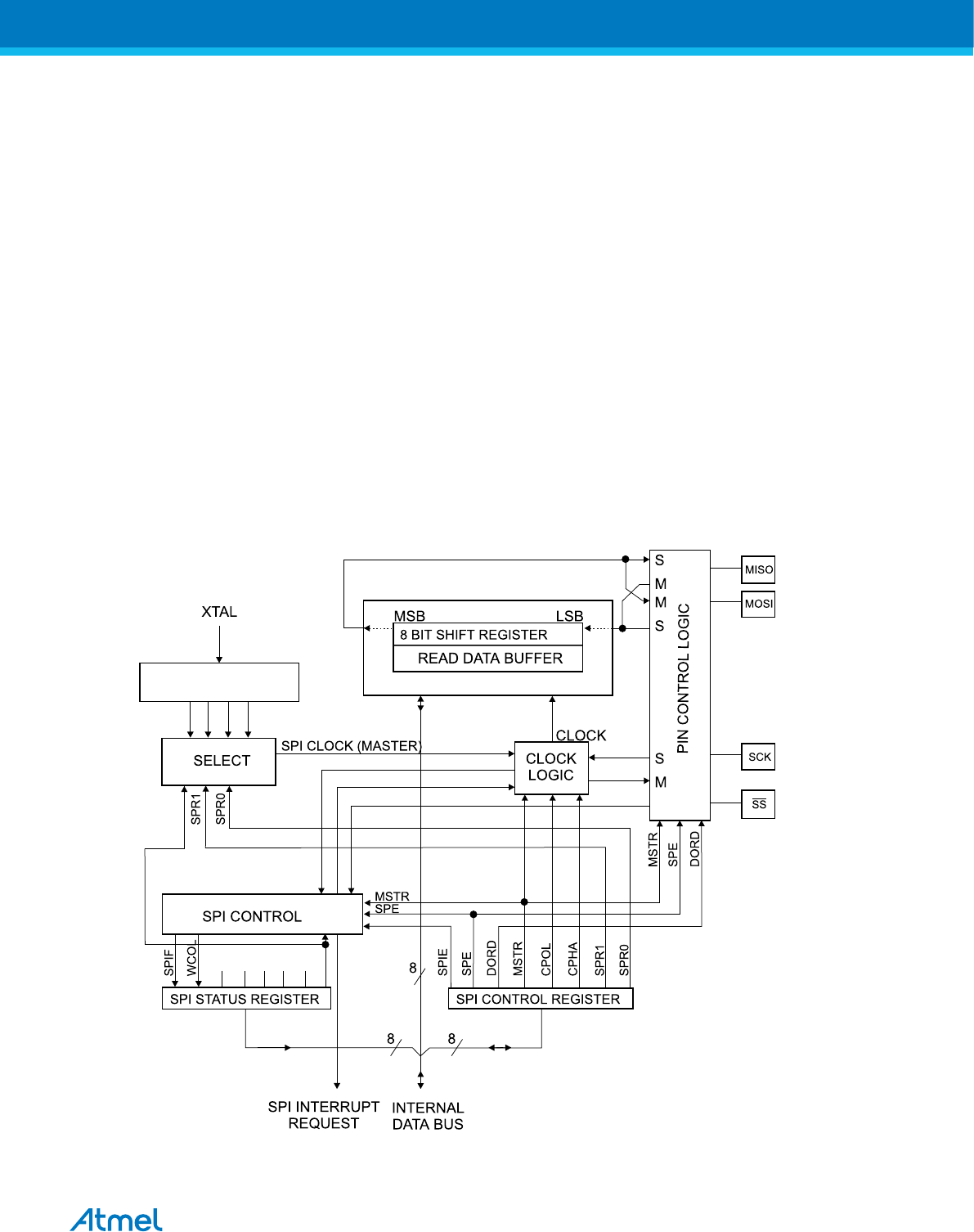
23. SPI – Serial Peripheral Interface
23.1. Features
•Full-duplex, Three-wire Synchronous Data Transfer
•Master or Slave Operation
•LSB First or MSB First Data Transfer
•Seven Programmable Bit Rates
•End of Transmission Interrupt Flag
•Write Collision Flag Protection
•Wake-up from Idle Mode
•Double Speed (CK/2) Master SPI Mode
23.2. Overview
The Serial Peripheral Interface (SPI) allows high-speed synchronous data transfer between the
ATmega8A and peripheral devices or between several AVR devices.
Figure 23-1 SPI Block Diagram(1)
SPI2X
SPI2X
DIVIDER
/2/4/8/16/32/64/128
Note: 1. Refer to Pin Configurations, table Port B Pins Alternate Functions in Alternate Functions of Port
B for SPI pin placement.
Atmel ATmega8A [DATASHEET]
Atmel-8159F-8-bit AVR Microcontroller_Datasheet_Complete-09/2015
170
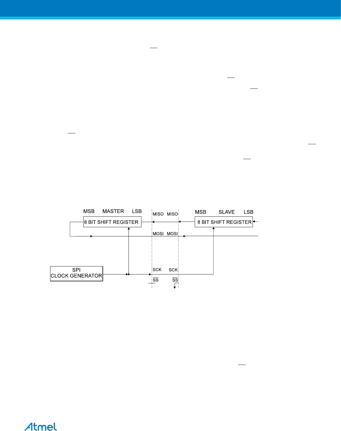
The interconnection between Master and Slave CPUs with SPI is shown in the figure below. The system
consists of two shift registers, and a Master Clock generator. The SPI Master initiates the communication
cycle when pulling low the Slave Select SS pin of the desired Slave. Master and Slave prepare the data
to be sent in their respective Shift Registers, and the Master generates the required clock pulses on the
SCK line to interchange data. Data is always shifted from Master to Slave on the Master Out – Slave In,
MOSI, line, and from Slave to Master on the Master In – Slave Out, MISO, line. After each data packet,
the Master will synchronize the Slave by pulling high the Slave Select, SS, line.
When configured as a Master, the SPI interface has no automatic control of the SS line. This must be
handled by user software before communication can start. When this is done, writing a byte to the SPI
Data Register starts the SPI clock generator, and the hardware shifts the eight bits into the Slave. After
shifting one byte, the SPI clock generator stops, setting the end of Transmission Flag (SPIF). If the SPI
interrupt enable bit (SPIE) in the SPCR Register is set, an interrupt is requested. The Master may
continue to shift the next byte by writing it into SPDR, or signal the end of packet by pulling high the Slave
Select, SS line. The last incoming byte will be kept in the Buffer Register for later use.
When configured as a Slave, the SPI interface will remain sleeping with MISO tri-stated as long as the SS
pin is driven high. In this state, software may update the contents of the SPI Data Register, SPDR, but the
data will not be shifted out by incoming clock pulses on the SCK pin until the SS pin is driven low. As one
byte has been completely shifted, the end of Transmission Flag, SPIF is set. If the SPI Interrupt Enable
bit, SPIE, in the SPCR Register is set, an interrupt is requested. The Slave may continue to place new
data to be sent into SPDR before reading the incoming data. The last incoming byte will be kept in the
Buffer Register for later use.
Figure 23-2 SPI Master-slave Interconnection
SHIFT
ENABLE
V
cc
The system is single buffered in the transmit direction and double buffered in the receive direction. This
means that bytes to be transmitted cannot be written to the SPI Data Register before the entire shift cycle
is completed. When receiving data, however, a received character must be read from the SPI Data
Register before the next character has been completely shifted in. Otherwise, the first byte is lost.
In SPI Slave mode, the control logic will sample the incoming signal of the SCK pin. To ensure correct
sampling of the clock signal, the minimum low and high periods should be:
Low period: longer than 2 CPU clock cycles.
High period: longer than 2 CPU clock cycles.
When the SPI is enabled, the data direction of the MOSI, MISO, SCK, and SS pins is overridden
according to the table below. For more details on automatic port overrides, refer to Alternate Port
Functions.
Atmel ATmega8A [DATASHEET]
Atmel-8159F-8-bit AVR Microcontroller_Datasheet_Complete-09/2015
171

Table 23-1 SPI Pin Overrides(1)
Pin Direction, Master SPI Direction, Slave SPI
MOSI User Defined Input
MISO Input User Defined
SCK User Defined Input
SS User Defined Input
Note: 1. Refer to table Port B Pins Alternate Functions in Alternate Functions of Port B for a detailed
description of how to define the direction of the user defined SPI pins.
The following code examples show how to initialize the SPI as a Master and how to perform a simple
transmission. DDR_SPI in the examples must be replaced by the actual Data Direction Register
controlling the SPI pins. DD_MOSI, DD_MISO and DD_SCK must be replaced by the actual data direction
bits for these pins. E.g. if MOSI is placed on pin PB5, replace DD_MOSI with DDB5 and DDR_SPI with
DDRB.
Assembly Code Example(1)
SPI_MasterInit:
; Set MOSI and SCK output, all others input
ldi r17,(1<<DD_MOSI)|(1<<DD_SCK)
out DDR_SPI,r17
; Enable SPI, Master, set clock rate fck/16
ldi r17,(1<<SPE)|(1<<MSTR)|(1<<SPR0)
out SPCR,r17
ret
SPI_MasterTransmit:
; Start transmission of data (r16)
out SPDR,r16
Wait_Transmit:
; Wait for transmission complete
sbis SPSR,SPIF
rjmp Wait_Transmit
ret
C Code Example(1)
void SPI_MasterInit(void)
{
/* Set MOSI and SCK output, all others input */
DDR_SPI = (1<<DD_MOSI)|(1<<DD_SCK);
/* Enable SPI, Master, set clock rate fck/16 */
SPCR = (1<<SPE)|(1<<MSTR)|(1<<SPR0);
}
void SPI_MasterTransmit(char cData)
{
/* Start transmission */
SPDR = cData;
/* Wait for transmission complete */
while(!(SPSR & (1<<SPIF)))
;
}
Atmel ATmega8A [DATASHEET]
Atmel-8159F-8-bit AVR Microcontroller_Datasheet_Complete-09/2015
172

Note: 1. See About Code Examples.
The following code examples show how to initialize the SPI as a Slave and how to
perform a simple reception.
Assembly Code Example(1)
SPI_SlaveInit:
; Set MISO output, all others input
ldi r17,(1<<DD_MISO)
out DDR_SPI,r17
; Enable SPI
ldi r17,(1<<SPE)
out SPCR,r17
ret
SPI_SlaveReceive:
; Wait for reception complete
sbis SPSR,SPIF
rjmp SPI_SlaveReceive
; Read received data and return
in r16,SPDR
ret
C Code Example(1)
void SPI_SlaveInit(void)
{
/* Set MISO output, all others input */
DDR_SPI = (1<<DD_MISO);
/* Enable SPI */
SPCR = (1<<SPE);
}
char SPI_SlaveReceive(void)
{
/* Wait for reception complete */
while(!(SPSR & (1<<SPIF)))
;
/* Return Data Register */
return SPDR;
}
Note: 1. See About Code Examples.
Related Links
Pin Configurations on page 13
Alternate Functions of Port B on page 83
Alternate Port Functions on page 81
About Code Examples on page 23
23.3. SS Pin Functionality
23.3.1. Slave Mode
When the SPI is configured as a Slave, the Slave Select (SS) pin is always input. When SS is held low,
the SPI is activated, and MISO becomes an output if configured so by the user. All other pins are inputs.
Atmel ATmega8A [DATASHEET]
Atmel-8159F-8-bit AVR Microcontroller_Datasheet_Complete-09/2015
173

When SS is driven high, all pins are inputs, and the SPI is passive, which means that it will not receive
incoming data. The SPI logic will be reset once the SS pin is driven high.
The SS pin is useful for packet/byte synchronization to keep the slave bit counter synchronous with the
master clock generator. When the SS pin is driven high, the SPI slave will immediately reset the send and
receive logic, and drop any partially received data in the Shift Register.
23.3.2. Master Mode
When the SPI is configured as a Master (MSTR in SPCR is set), the user can determine the direction of
the SS pin.
If SS is configured as an output, the pin is a general output pin which does not affect the SPI system.
Typically, the pin will be driving the SS pin of the SPI Slave.
If SS is configured as an input, it must be held high to ensure Master SPI operation. If the SS pin is driven
low by peripheral circuitry when the SPI is configured as a Master with the SS pin defined as an input, the
SPI system interprets this as another master selecting the SPI as a slave and starting to send data to it.
To avoid bus contention, the SPI system takes the following actions:
1. The MSTR bit in SPCR is cleared and the SPI system becomes a Slave. As a result of the SPI
becoming a Slave, the MOSI and SCK pins become inputs.
2. The SPIF Flag in SPSR is set, and if the SPI interrupt is enabled, and the I-bit in SREG is set, the
interrupt routine will be executed.
Thus, when interrupt-driven SPI transmission is used in Master mode, and there exists a possibility that
SS is driven low, the interrupt should always check that the MSTR bit is still set. If the MSTR bit has been
cleared by a slave select, it must be set by the user to re-enable SPI Master mode.
23.4. Data Modes
There are four combinations of SCK phase and polarity with respect to serial data, which are determined
by control bits CPHA and CPOL. The SPI data transfer formats are shown in the figures in this section.
Data bits are shifted out and latched in on opposite edges of the SCK signal, ensuring sufficient time for
data signals to stabilize. This is clearly seen by summarizing Table 23-3 CPOL Functionality on page
176 and Table 23-4 CPHA Functionality on page 177, as done below:
Table 23-2 CPOL and CPHA Functionality
SPI Mode Conditions Leading Edge Trailing Edge
0 CPOL=0, CPHA=0 Sample (Rising) Setup (Falling)
1 CPOL=0, CPHA=1 Setup (Rising) Sample (Falling)
2 CPOL=1, CPHA=0 Sample (Falling) Setup (Rising)
3 CPOL=1, CPHA=1 Setup (Falling) Sample (Rising)
Atmel ATmega8A [DATASHEET]
Atmel-8159F-8-bit AVR Microcontroller_Datasheet_Complete-09/2015
174
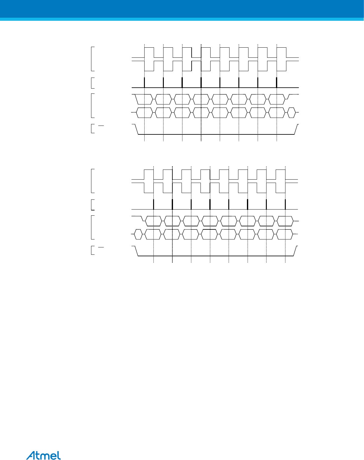
Figure 23-3 SPI Transfer Format with CPHA = 0
Bit 1
Bit 6
LSB
MSB
SCK (CPOL = 0)
mode 0
SAMPLE I
MOSI/MISO
CHANGE 0
MOSI PIN
CHANGE 0
MISO PIN
SCK (CPOL = 1)
mode 2
SS
MSB
LSB
Bit 6
Bit 1
Bit 5
Bit 2
Bit 4
Bit 3
Bit 3
Bit 4
Bit 2
Bit 5
MSB first (DORD = 0)
LSB first (DORD = 1)
Figure 23-4 SPI Transfer Format with CPHA = 1
SCK (CPOL = 0)
mode 1
SAMPLE I
MOSI/MISO
CHANGE 0
MOSI PIN
CHANGE 0
MISO PIN
SCK (CPOL = 1)
mode 3
SS
MSB
LSB
Bit 6
Bit 1
Bit 5
Bit 2
Bit 4
Bit 3
Bit 3
Bit 4
Bit 2
Bit 5
Bit 1
Bit 6
LSB
MSB
MSB first (DORD = 0)
LSB first (DORD = 1)
23.5. Register Description
Atmel ATmega8A [DATASHEET]
Atmel-8159F-8-bit AVR Microcontroller_Datasheet_Complete-09/2015
175
23.5.1. SPCR – SPI Control Register
When using the I/O specific commands IN and OUT, the I/O addresses 0x00 - 0x3F must be used. When
addressing I/O Registers as data space using LD and ST instructions, 0x20 must be added to these offset
addresses. The device is a complex microcontroller with more peripheral units than can be supported
within the 64 location reserved in Opcode for the IN and OUT instructions. For the Extended I/O space
from 0x60 in SRAM, only the ST/STS/STD and LD/LDS/LDD instructions can be used.
Name: SPCR
Offset: 0x0D
Reset: 0x00
Property:
When addressing I/O Registers as data space the offset address is 0x2D
Bit 7 6 5 4 3 2 1 0
SPIE SPE DORD MSTR CPOL CPHA SPR1 SPR0
Access R/W R/W R/W R/W R/W R/W R/W R/W
Reset 0 0 0 0 0 0 0 0
Bit 7 – SPIE: SPI Interrupt Enable
This bit causes the SPI interrupt to be executed if SPIF bit in the SPSR Register is set and if the Global
Interrupt Enable bit in SREG is set.
Bit 6 – SPE: SPI Enable
When the SPE bit is written to one, the SPI is enabled. This bit must be set to enable any SPI operations.
Bit 5 – DORD: Data Order
When the DORD bit is written to one, the LSB of the data word is transmitted first.
When the DORD bit is written to zero, the MSB of the data word is transmitted first.
Bit 4 – MSTR: Master/Slave Select
This bit selects Master SPI mode when written to one, and Slave SPI mode when written logic zero. If SS
is configured as an input and is driven low while MSTR is set, MSTR will be cleared, and SPIF in SPSR
will become set. The user will then have to set MSTR to re-enable SPI Master mode.
Bit 3 – CPOL: Clock Polarity
When this bit is written to one, SCK is high when idle. When CPOL is written to zero, SCK is low when
idle. Refer to the figures in Data Modes on page 174 for an example. The CPOL functionality is
summarized below:
Table 23-3 CPOL Functionality
CPOL Leading Edge Trailing Edge
0 Rising Falling
1 Falling Rising
Bit 2 – CPHA: Clock Phase
The settings of the Clock Phase bit (CPHA) determine if data is sampled on the leading (first) or trailing
(last) edge of SCK. Refer to the figures in Data Modes on page 174 for an example. The CPHA
functionality is summarized below:
Atmel ATmega8A [DATASHEET]
Atmel-8159F-8-bit AVR Microcontroller_Datasheet_Complete-09/2015
176

Table 23-4 CPHA Functionality
CPHA Leading Edge Trailing Edge
0 Sample Setup
1 Setup Sample
Bits 1:0 – SPRn: SPI Clock Rate Select [n = 1:0]
These two bits control the SCK rate of the device configured as a Master. SPR1 and SPR0 have no effect
on the Slave. The relationship between SCK and the Oscillator Clock frequency fosc is shown in the table
below.
Table 23-5 Relationship between SCK and Oscillator Frequency
SPI2X SPR1 SPR0 SCK Frequency
0 0 0 fosc/4
0 0 1 fosc/16
0 1 0 fosc/64
0 1 1 fosc/128
1 0 0 fosc/2
1 0 1 fosc/8
1 1 0 fosc/32
1 1 1 fosc/64
Atmel ATmega8A [DATASHEET]
Atmel-8159F-8-bit AVR Microcontroller_Datasheet_Complete-09/2015
177
23.5.2. SPSR – SPI Status Register
When using the I/O specific commands IN and OUT, the I/O addresses 0x00 - 0x3F must be used. When
addressing I/O Registers as data space using LD and ST instructions, 0x20 must be added to these offset
addresses. The device is a complex microcontroller with more peripheral units than can be supported
within the 64 location reserved in Opcode for the IN and OUT instructions. For the Extended I/O space
from 0x60 in SRAM, only the ST/STS/STD and LD/LDS/LDD instructions can be used.
Name: SPSR
Offset: 0x0E
Reset: 0x00
Property:
When addressing I/O Registers as data space the offset address is 0x2E
Bit 7 6 5 4 3 2 1 0
SPIF WCOL SPI2X
Access R R R/W
Reset 0 0 0
Bit 7 – SPIF: SPI Interrupt Flag
When a serial transfer is complete, the SPIF Flag is set. An interrupt is generated if SPIE in SPCR is set
and global interrupts are enabled. If SS is an input and is driven low when the SPI is in Master mode, this
will also set the SPIF Flag. SPIF is cleared by hardware when executing the corresponding interrupt
handling vector. Alternatively, the SPIF bit is cleared by first reading the SPI Status Register with SPIF
set, then accessing the SPI Data Register (SPDR).
Bit 6 – WCOL: Write Collision Flag
The WCOL bit is set if the SPI Data Register (SPDR) is written during a data transfer. The WCOL bit (and
the SPIF bit) are cleared by first reading the SPI Status Register with WCOL set, and then accessing the
SPI Data Register.
Bit 0 – SPI2X: Double SPI Speed Bit
When this bit is written logic one the SPI speed (SCK Frequency) will be doubled when the SPI is in
Master mode (refer to Table 23-5 Relationship between SCK and Oscillator Frequency on page 177).
This means that the minimum SCK period will be two CPU clock periods. When the SPI is configured as
Slave, the SPI is only guaranteed to work at fosc/4 or lower.
The SPI interface on the ATmega8A is also used for program memory and EEPROM downloading or
uploading. Refer to section Serial Downloading in Memory Programming for serial programming and
verification.
Atmel ATmega8A [DATASHEET]
Atmel-8159F-8-bit AVR Microcontroller_Datasheet_Complete-09/2015
178

23.5.3. SPDR – SPI Data Register is a read/write register
When using the I/O specific commands IN and OUT, the I/O addresses 0x00 - 0x3F must be used. When
addressing I/O Registers as data space using LD and ST instructions, 0x20 must be added to these offset
addresses. The device is a complex microcontroller with more peripheral units than can be supported
within the 64 location reserved in Opcode for the IN and OUT instructions. For the Extended I/O space
from 0x60 in SRAM, only the ST/STS/STD and LD/LDS/LDD instructions can be used.
Name: SPDR
Offset: 0x0F
Reset: 0xXX
Property:
When addressing I/O Registers as data space the offset address is 0x2F
Bit 7 6 5 4 3 2 1 0
SPID7 SPID6 SPID5 SPID4 SPID3 SPID2 SPID1 SPID0
Access R/W R/W R/W R/W R/W R/W R/W R/W
Reset x x x x x x x x
Bits 7:0 – SPIDn: SPI Data
The SPI Data Register is a read/write register used for data transfer between the Register File and the
SPI Shift Register. Writing to the register initiates data transmission. Reading the register causes the Shift
Register Receive buffer to be read.
•SPID7 is MSB
•SPID0 is LSB
Atmel ATmega8A [DATASHEET]
Atmel-8159F-8-bit AVR Microcontroller_Datasheet_Complete-09/2015
179

24. USART - Universal Synchronous and Asynchronous serial Receiver
and Transmitter
24.1. Features
•Full Duplex Operation (Independent Serial Receive and Transmit Registers)
•Asynchronous or Synchronous Operation
•Master or Slave Clocked Synchronous Operation
•High Resolution Baud Rate Generator
•Supports Serial Frames with 5, 6, 7, 8, or 9 data bits and 1 or 2 stop bits
•Odd or Even Parity Generation and Parity Check Supported by Hardware
•Data OverRun Detection
•Framing Error Detection
•Noise Filtering Includes False Start Bit Detection and Digital Low Pass Filter
•Three Separate Interrupts on TX Complete, TX Data Register Empty and RX Complete
•Multi-processor Communication Mode
•Double Speed Asynchronous Communication Mode
24.2. Overview
The Universal Synchronous and Asynchronous serial Receiver and Transmitter (USART) is a highly-
flexible serial communication device. A simplified block diagram of the USART Transmitter is shown in the
figure below. CPU accessible I/O Registers and I/O pins are shown in bold.
Atmel ATmega8A [DATASHEET]
Atmel-8159F-8-bit AVR Microcontroller_Datasheet_Complete-09/2015
180
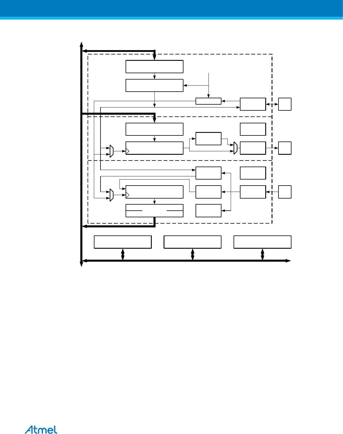
Figure 24-1 USART Block Diagram(1)
PARITY
GENERATOR
UBRRn [H:L]
UDRn(Transmit)
UCSRnA UCSRnB UCSRnC
BAUD RATE GENERATOR
TRANSMIT SHIFT REGISTER
RECEIVE SHIFT REGISTER RxDn
TxDn
PIN
CONTROL
UDRn (Receive)
PIN
CONTROL
XCKn
DATA
RECOVERY
CLOCK
RECOVERY
PIN
CONTROL
TX
CONTROL
RX
CONTROL
PARITY
CHECKER
DATA BUS
OSC
SYNC LOGIC
Clock Generator
Transmitter
Receiver
Note: 1. Refer to Pin Configurations, table Overriding Signals for Alternate Functions PD7:PD4 and
table Overriding Signals for Alternate Functions in PD3:PD0 in Alternate Functions of Port D for USART
pin placement.
The dashed boxes in the block diagram separate the three main parts of the USART (listed from the top):
Clock generator, Transmitter and Receiver. Control Registers are shared by all units. The clock
generation logic consists of synchronization logic for external clock input used by synchronous slave
operation, and the baud rate generator. The XCK (transfer clock) pin is only used by synchronous transfer
mode. The Transmitter consists of a single write buffer, a serial Shift Register, Parity Generator and
control logic for handling different serial frame formats. The write buffer allows a continuous transfer of
data without any delay between frames. The Receiver is the most complex part of the USART module
due to its clock and data recovery units. The recovery units are used for asynchronous data reception. In
addition to the recovery units, the Receiver includes a parity checker, control logic, a Shift Register and a
two level receive buffer (UDR). The Receiver supports the same frame formats as the Transmitter, and
can detect Frame Error, Data OverRun and Parity Errors.
Related Links
Pin Configurations on page 13
Alternate Functions of Port D on page 88
Atmel ATmega8A [DATASHEET]
Atmel-8159F-8-bit AVR Microcontroller_Datasheet_Complete-09/2015
181

24.2.1. AVR USART vs. AVR UART – Compatibility
The USART is fully compatible with the AVR UART regarding:
•Bit locations inside all USART Registers.
•Baud Rate Generation.
•Transmitter Operation.
•Transmit Buffer Functionality.
•Receiver Operation.
However, the receive buffering has two improvements that will affect the compatibility in some special
cases:
•A second Buffer Register has been added. The two Buffer Registers operate as a circular FIFO
buffer. Therefore the UDR must only be read once for each incoming data! More important is the
fact that the Error Flags (FE and DOR) and the ninth data bit (RXB8) are buffered with the data in
the receive buffer. Therefore the status bits must always be read before the UDR Register is read.
Otherwise the error status will be lost since the buffer state is lost.
•The Receiver Shift Register can now act as a third buffer level. This is done by allowing the
received data to remain in the serial Shift Register (see Block Diagram in previous section) if the
Buffer Registers are full, until a new start bit is detected. The USART is therefore more resistant to
Data OverRun (DOR) error conditions.
The following control bits have changed name, but have same functionality and register location:
•CHR9 is changed to UCSZ2.
•OR is changed to DOR.
24.3. Clock Generation
The clock generation logic generates the base clock for the Transmitter and Receiver. The USART
supports four modes of clock operation: normal asynchronous, double speed asynchronous, Master
synchronous and Slave Synchronous mode. The UMSEL bit in USART Control and Status Register C
(UCSRC) selects between asynchronous and synchronous operation. Double speed (Asynchronous
mode only) is controlled by the U2X found in the UCSRA Register. When using Synchronous mode
(UMSEL = 1), the Data Direction Register for the XCK pin (DDR_XCK) controls whether the clock source
is internal (Master mode) or external (Slave mode). The XCK pin is only active when using Synchronous
mode.
Below is a block diagram of the clock generation logic.
Atmel ATmega8A [DATASHEET]
Atmel-8159F-8-bit AVR Microcontroller_Datasheet_Complete-09/2015
182
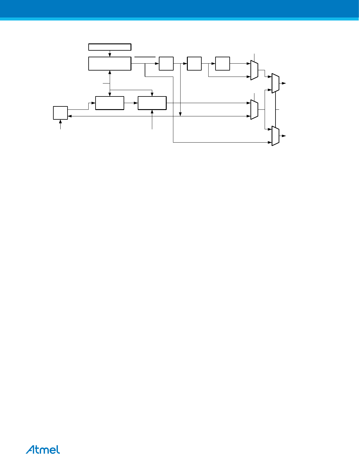
Figure 24-2 Clock Generation Logic, Block Diagram
Prescaling
Down-Counter /2
UBRRn
/4 /2
foscn
UBRRn+1
Sync
Register
OSC
XCKn
Pin
txclk
U2Xn
UMSELn
DDR_XCKn
0
1
0
1
xcki
xcko
DDR_XCKn rxclk
0
1
1
0
Edge
Detector
UCPOLn
Signal description:
txclk Transmitter clock (internal signal).
rxclk Receiver base clock (internal signal).
xcki Input from XCK pin (internal Signal). Used for synchronous slave operation.
xcko Clock output to XCK pin (internal signal). Used for synchronous master operation.
fosc XTAL pin frequency (System Clock).
24.3.1. Internal Clock Generation – The Baud Rate Generator
Internal clock generation is used for the asynchronous and the synchronous master modes of operation.
The description in this section refers to the block diagram above.
The USART Baud Rate Register (UBRR) and the down-counter connected to it function as a
programmable prescaler or baud rate generator. The down-counter, running at system clock (fosc), is
loaded with the UBRR value each time the counter has counted down to zero or when the UBRRL
Register is written. A clock is generated each time the counter reaches zero. This clock is the baud rate
generator clock output (= fosc/(UBRR+1)). The Transmitter divides the baud rate generator clock output
by 2, 8, or 16 depending on mode. The baud rate generator output is used directly by the Receiver’s clock
and data recovery units. However, the recovery units use a state machine that uses 2, 8, or 16 states
depending on mode set by the state of the UMSEL, U2X and DDR_XCK bits.
The table below contains equations for calculating the baud rate (in bits per second) and for calculating
the UBRR value for each mode of operation using an internally generated clock source.
Atmel ATmega8A [DATASHEET]
Atmel-8159F-8-bit AVR Microcontroller_Datasheet_Complete-09/2015
183
Table 24-1 Equations for Calculating Baud Rate Register Setting
Operating Mode Equation for Calculating Baud
Rate(1)
Equation for Calculating UBRR
Value
Asynchronous Normal
mode (U2X = 0) BAUD = OSC
16 + 1 =OSC
16BAUD 1
Asynchronous Double
Speed mode (U2X = 1) BAUD = OSC
8 + 1 =OSC
8BAUD 1
Synchronous Master mode BAUD = OSC
2+1 =OSC
2BAUD 1
Note: 1. The baud rate is defined to be the transfer rate in bit per second (bps).
BAUD Baud rate (in bits per second, bps).
fOSC System oscillator clock frequency.
UBRR Contents of the UBRRH and UBRRL Registers, (0-4095).
Some examples of UBRR values for some system clock frequencies are found in Table 24-9 Examples of
UBRR Settings for Commonly Used Oscillator Frequencies on page 207.
24.3.2. Double Speed Operation (U2X)
The transfer rate can be doubled by setting the U2X bit in UCSRA. Setting this bit only has effect for the
asynchronous operation. Set this bit to zero when using synchronous operation.
Setting this bit will reduce the divisor of the baud rate divider from 16 to 8, effectively doubling the transfer
rate for asynchronous communication. Note however that the Receiver will in this case only use half the
number of samples (reduced from 16 to 8) for data sampling and clock recovery, and therefore a more
accurate baud rate setting and system clock are required when this mode is used.
For the Transmitter, there are no downsides.
24.3.3. External Clock
External clocking is used by the synchronous slave modes of operation. The description in this section
refers to Figure 24-2 Clock Generation Logic, Block Diagram on page 183.
External clock input from the XCK pin is sampled by a synchronization register to minimize the chance of
meta-stability. The output from the synchronization register must then pass through an edge detector
before it can be used by the Transmitter and Receiver. This process introduces a two CPU clock period
delay and therefore the maximum external XCK clock frequency is limited by the following equation:
XCK <OSC
4
The value of fosc depends on the stability of the system clock source. It is therefore recommended to add
some margin to avoid possible loss of data due to frequency variations.
24.3.4. Synchronous Clock Operation
When Synchronous mode is used (UMSEL = 1), the XCK pin will be used as either clock input (Slave) or
clock output (Master). The dependency between the clock edges and data sampling or data change is the
same. The basic principle is that data input (on RxD) is sampled at the opposite XCK clock edge of the
edge the data output (TxD) is changed.
Atmel ATmega8A [DATASHEET]
Atmel-8159F-8-bit AVR Microcontroller_Datasheet_Complete-09/2015
184
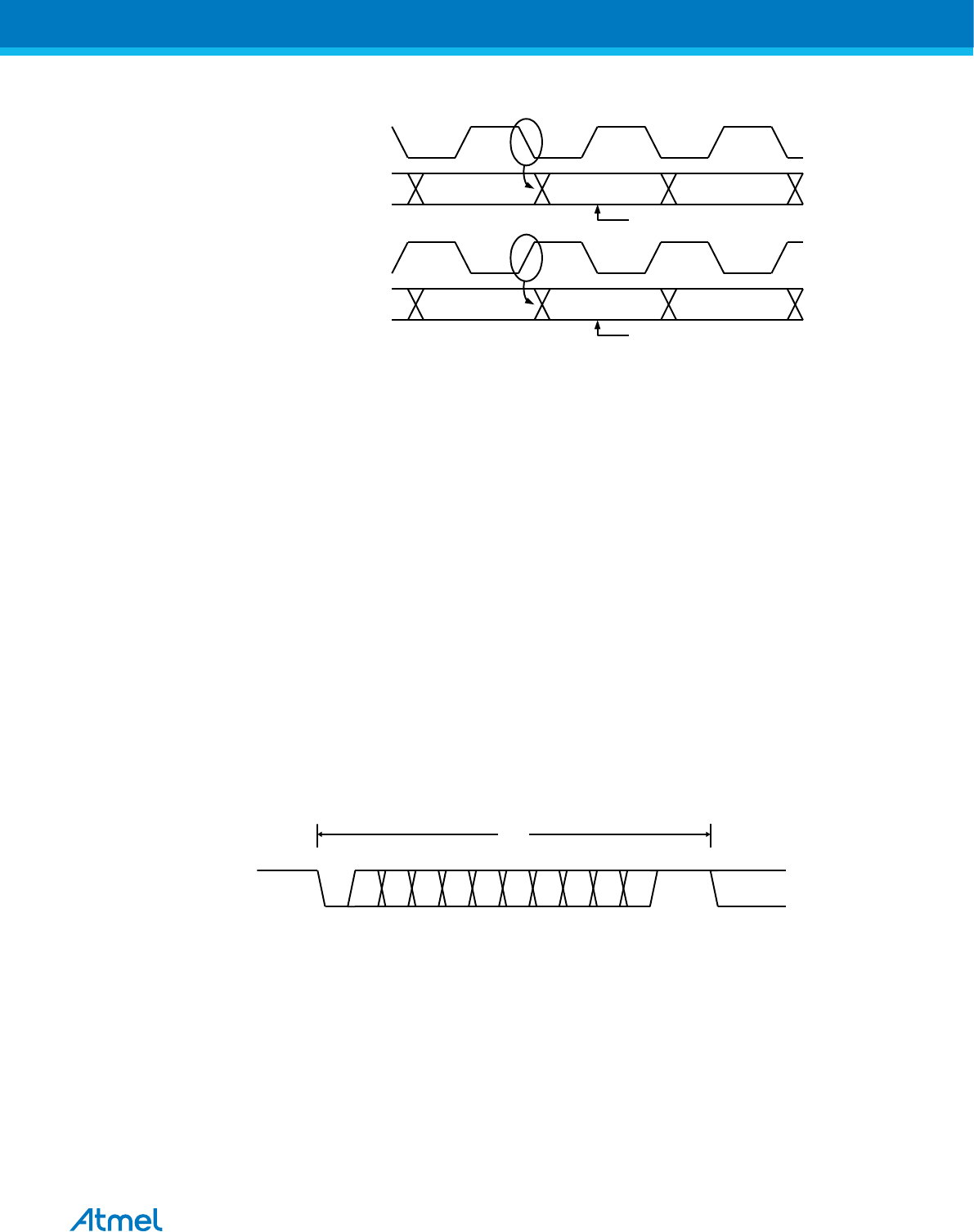
Figure 24-3 Synchronous Mode XCK Timing
RxD / TxD
XCK
RxD / TxD
XCK UCPOL = 0
UCPOL = 1
Sample
Sample
The UCPOL bit UCRSC selects which XCK clock edge is used for data sampling and which is used for
data change. As the figure above shows, when UCPOL is zero the data will be changed at rising XCK
edge and sampled at falling XCK edge. If UCPOL is set, the data will be changed at falling XCK edge and
sampled at rising XCK edge.
24.4. Frame Formats
A serial frame is defined to be one character of data bits with synchronization bits (start and stop bits),
and optionally a parity bit for error checking. The USART accepts all 30 combinations of the following as
valid frame formats:
•1 start bit
•5, 6, 7, 8, or 9 data bits
•no, even or odd parity bit
•1 or 2 stop bits
A frame starts with the start bit followed by the least significant data bit. Then the next data bits, up to a
total of nine, are succeeding, ending with the most significant bit. If enabled, the parity bit is inserted after
the data bits, before the stop bits. When a complete frame is transmitted, it can be directly followed by a
new frame, or the communication line can be set to an idle (high) state. The figure below illustrates the
possible combinations of the frame formats. Bits inside brackets are optional.
Figure 24-4 Frame Formats
10 2 3 4 [5] [6] [7] [8] [P]St Sp1 [Sp2] (St / IDLE)(IDLE)
FRAME
St Start bit, always low.
(n) Data bits (0 to 8).
PParity bit. Can be odd or even.
Sp Stop bit, always high.
IDLE No transfers on the communication line (RxD or TxD). An IDLE line must be high.
The frame format used by the USART is set by the UCSZ2:0, UPM1:0 and USBS bits in UCSRB and
UCSRC. The Receiver and Transmitter use the same setting. Note that changing the setting of any of
these bits will corrupt all ongoing communication for both the Receiver and Transmitter.
Atmel ATmega8A [DATASHEET]
Atmel-8159F-8-bit AVR Microcontroller_Datasheet_Complete-09/2015
185

The USART Character Size (UCSZ2:0) bits select the number of data bits in the frame. The USART
Parity mode (UPM1:0) bits enable and set the type of parity bit. The selection between one or two stop
bits is done by the USART Stop Bit Select (USBS) bit. The Receiver ignores the second stop bit. An FE
(Frame Error) will therefore only be detected in the cases where the first stop bit is zero
24.4.1. Parity Bit Calculation
The parity bit is calculated by doing an exclusive-or of all the data bits. If odd parity is used, the result of
the exclusive or is inverted. The relation between the parity bit and data bits is as follows:
even =1… 3 2 1 01
odd =1… 3 2 1 01
Peven Parity bit using even parity
Podd Parity bit using odd parity
dnData bit n of the character
If used, the parity bit is located between the last data bit and first stop bit of a serial frame.
24.5. USART Initialization
The USART has to be initialized before any communication can take place. The initialization process
normally consists of setting the baud rate, setting frame format and enabling the Transmitter or the
Receiver depending on the usage. For interrupt driven USART operation, the Global Interrupt Flag should
be cleared (and interrupts globally disabled) when doing the initialization.
Before doing a re-initialization with changed baud rate or frame format, be sure that there are no ongoing
transmissions during the period the registers are changed. The TXC Flag can be used to check that the
Transmitter has completed all transfers, and the RXC Flag can be used to check that there are no unread
data in the receive buffer. Note that the TXC Flag must be cleared before each transmission (before UDR
is written) if it is used for this purpose.
The following simple USART initialization code examples show one assembly and one C function that are
equal in functionality. The examples assume asynchronous operation using polling (no interrupts enabled)
and a fixed frame format. The baud rate is given as a function parameter. For the assembly code, the
baud rate parameter is assumed to be stored in the r17:r16 Registers. When the function writes to the
UCSRC Register, the URSEL bit (MSB) must be set due to the sharing of I/O location by UBRRH and
UCSRC.
Assembly Code Example(1)
USART_Init:
; Set baud rate
out UBRRH, r17
out UBRRL, r16
; Enable receiver and transmitter
ldi r16, (1<<RXEN)|(1<<TXEN)
out UCSRB,r16
; Set frame format: 8data, 2stop bit
ldi r16, (1<<URSEL)|(1<<USBS)|(3<<UCSZ0)
out UCSRC,r16
ret
Atmel ATmega8A [DATASHEET]
Atmel-8159F-8-bit AVR Microcontroller_Datasheet_Complete-09/2015
186

C Code Example(1)
#define FOSC 1843200 // Clock Speed
#define BAUD 9600
#define MYUBRR FOSC/16/BAUD-1
void main( void )
{
...
USART_Init(MYUBRR)
...
}
void USART_Init( unsigned int ubrr)
{
/*Set baud rate */
UBRR0H = (unsigned char)(ubrr>>8);
UBRR0L = (unsigned char)ubrr;
Enable receiver and transmitter */
UCSRB = (1<<RXEN)|(1<<TXEN);
/* Set frame format: 8data, 2stop bit */
UCSRC = (1<<URSEL)|(1<<USBS)|(3<<UCSZ0);
}
Note: 1. See About Code Examples.
More advanced initialization routines can be written to include frame format as
parameters, disable interrupts, and so on. However, many applications use a fixed setting
of the baud and control registers, and for these types of applications the initialization
code can be placed directly in the main routine, or be combined with initialization code for
other I/O modules.
Related Links
About Code Examples on page 23
24.6. Data Transmission – The USART Transmitter
The USART Transmitter is enabled by setting the Transmit Enable (TXEN) bit in the UCSRB Register.
When the Transmitter is enabled, the normal port operation of the TxD pin is overridden by the USART
and given the function as the Transmitter’s serial output. The baud rate, mode of operation and frame
format must be set up once before doing any transmissions. If synchronous operation is used, the clock
on the XCK pin will be overridden and used as transmission clock.
24.6.1. Sending Frames with 5 to 8 Data Bits
A data transmission is initiated by loading the transmit buffer with the data to be transmitted. The CPU
can load the transmit buffer by writing to the UDR I/O location. The buffered data in the transmit buffer will
be moved to the Shift Register when the Shift Register is ready to send a new frame. The Shift Register is
loaded with new data if it is in idle state (no ongoing transmission) or immediately after the last stop bit of
the previous frame is transmitted. When the Shift Register is loaded with new data, it will transfer one
complete frame at the rate given by the Baud Register, U2X bit or by XCK depending on mode of
operation.
The following code examples show a simple USART transmit function based on polling of the Data
Register Empty (UDRE) Flag. When using frames with less than eight bits, the most significant bits
written to the UDR are ignored. The USART has to be initialized before the function can be used. For the
assembly code, the data to be sent is assumed to be stored in Register R16.
Atmel ATmega8A [DATASHEET]
Atmel-8159F-8-bit AVR Microcontroller_Datasheet_Complete-09/2015
187

Assembly Code Example(1)
USART_Transmit:
; Wait for empty transmit buffer
sbis UCSRA,UDRE
rjmp USART_Transmit
; Put data (r16) into buffer, sends the data
out UDR,r16
ret
C Code Example(1)
void USART_Transmit( unsigned char data )
{
/* Wait for empty transmit buffer */
while ( !( UCSRA & (1<<UDRE)) )
;
/* Put data into buffer, sends the data */
UDR = data;
}
Note: 1. See About Code Examples.
The function simply waits for the transmit buffer to be empty by checking the UDRE Flag,
before loading it with new data to be transmitted. If the Data Register Empty Interrupt is
utilized, the interrupt routine writes the data into the buffer.
Related Links
About Code Examples on page 23
24.6.2. Sending Frames with 9 Data Bits
If 9-bit characters are used (UCSZ = 7), the ninth bit must be written to the TXB8 bit in UCSRB before the
Low byte of the character is written to UDR. The following code examples show a transmit function that
handles 9-bit characters. For the assembly code, the data to be sent is assumed to be stored in registers
R17:R16.
Assembly Code Example(1)
USART_Transmit:
; Wait for empty transmit buffer
sbis UCSRA,UDRE
rjmp USART_Transmit
; Copy 9th bit from r17 to TXB8
cbi UCSRB,TXB8
sbrc r17,0
sbi UCSRB,TXB8
; Put LSB data (r16) into buffer, sends the data
out UDR,r16
ret
C Code Example(1)
void USART_Transmit( unsigned int data )
{
/* Wait for empty transmit buffer */
while ( !( UCSRA & (1<<UDRE))) )
;
/* Copy 9th bit to TXB8 */
Atmel ATmega8A [DATASHEET]
Atmel-8159F-8-bit AVR Microcontroller_Datasheet_Complete-09/2015
188

UCSRB &= ~(1<<TXB8);
if ( data & 0x0100 )
UCSRB |= (1<<TXB8);
/* Put data into buffer, sends the data */
UDR = data;
}
Note: 1. These transmit functions are written to be general functions. They can be
optimized if the contents of the UCSRB is static. For example, only the TXB8 bit of the
UCSRB Register is used after initialization.
The ninth bit can be used for indicating an address frame when using multi processor
communication mode or for other protocol handling as for example synchronization.
24.6.3. Transmitter Flags and Interrupts
The USART Transmitter has two flags that indicate its state: USART Data Register Empty (UDRE) and
Transmit Complete (TXC). Both flags can be used for generating interrupts.
The Data Register Empty (UDRE) Flag indicates whether the transmit buffer is ready to receive new data.
This bit is set when the transmit buffer is empty, and cleared when the transmit buffer contains data to be
transmitted that has not yet been moved into the Shift Register. For compatibility with future devices,
always write this bit to zero when writing the UCSRA Register.
When the Data Register empty Interrupt Enable (UDRIE) bit in UCSRB is written to one, the USART Data
Register Empty Interrupt will be executed as long as UDRE is set (provided that global interrupts are
enabled). UDRE is cleared by writing UDR. When interrupt-driven data transmission is used, the Data
Register empty Interrupt routine must either write new data to UDR in order to clear UDRE or disable the
Data Register empty Interrupt, otherwise a new interrupt will occur once the interrupt routine terminates.
The Transmit Complete (TXC) Flag bit is set one when the entire frame in the transmit Shift Register has
been shifted out and there are no new data currently present in the transmit buffer. The TXC Flag bit is
automatically cleared when a transmit complete interrupt is executed, or it can be cleared by writing a one
to its bit location. The TXC Flag is useful in half-duplex communication interfaces (like the RS485
standard), where a transmitting application must enter Receive mode and free the communication bus
immediately after completing the transmission.
When the Transmit Compete Interrupt Enable (TXCIE) bit in UCSRB is set, the USART Transmit
Complete Interrupt will be executed when the TXC Flag becomes set (provided that global interrupts are
enabled). When the transmit complete interrupt is used, the interrupt handling routine does not have to
clear the TXC Flag, this is done automatically when the interrupt is executed.
24.6.4. Parity Generator
The Parity Generator calculates the parity bit for the serial frame data. When parity bit is enabled (UPM1
= 1), the Transmitter control logic inserts the parity bit between the last data bit and the first stop bit of the
frame that is sent.
24.6.5. Disabling the Transmitter
The disabling of the Transmitter (setting the TXEN to zero) will not become effective until ongoing and
pending transmissions are completed (i.e., when the Transmit Shift Register and Transmit Buffer Register
do not contain data to be transmitted). When disabled, the Transmitter will no longer override the TxD pin.
Atmel ATmega8A [DATASHEET]
Atmel-8159F-8-bit AVR Microcontroller_Datasheet_Complete-09/2015
189

24.7. Data Reception – The USART Receiver
The USART Receiver is enabled by writing the Receive Enable (RXEN) bit in the UCSRB Register to
one. When the Receiver is enabled, the normal pin operation of the RxD pin is overridden by the USART
and given the function as the Receiver’s serial input. The baud rate, mode of operation and frame format
must be set up once before any serial reception can be done. If synchronous operation is used, the clock
on the XCK pin will be used as transfer clock.
24.7.1. Receiving Frames with 5 to 8 Data Bits
The Receiver starts data reception when it detects a valid start bit. Each bit that follows the start bit will be
sampled at the baud rate or XCK clock, and shifted into the Receive Shift Register until the first stop bit of
a frame is received. A second stop bit will be ignored by the Receiver. When the first stop bit is received
(i.e., a complete serial frame is present in the Receive Shift Register), the contents of the Shift Register
will be moved into the receive buffer. The receive buffer can then be read by reading the UDR I/O
location.
The following code example shows a simple USART receive function based on polling of the Receive
Complete (RXC) Flag. When using frames with less than eight bits the most significant bits of the data
read from the UDR will be masked to zero. The USART has to be initialized before the function can be
used.
Assembly Code Example(1)
USART_Receive:
; Wait for data to be received
sbis UCSRA, RXC
rjmp USART_Receive
; Get and return received data from buffer
in r16, UDR
ret
C Code Example(1)
unsigned char USART_Receive( void )
{
/* Wait for data to be received */
while ( !(UCSRA & (1<<RXC)) )
;
/* Get and return received data from buffer */
return UDR;
}
Note: 1. See About Code Examples.
The function simply waits for data to be present in the receive buffer by checking the
RXC Flag, before reading the buffer and returning the value.
Related Links
About Code Examples on page 23
24.7.2. Receiving Frames with 9 Data Bits
If 9-bit characters are used (UCSZ=7) the ninth bit must be read from the RXB8 bit in UCSRB before
reading the low bits from the UDR. This rule applies to the FE, DOR and PE Status Flags as well. Read
status from UCSRA, then data from UDR. Reading the UDR I/O location will change the state of the
Atmel ATmega8A [DATASHEET]
Atmel-8159F-8-bit AVR Microcontroller_Datasheet_Complete-09/2015
190

receive buffer FIFO and consequently the TXB8, FE, DOR, and PE bits, which all are stored in the FIFO,
will change.
The following code example shows a simple USART receive function that handles both 9-bit characters
and the status bits.
Assembly Code Example(1)
USART_Receive:
; Wait for data to be received
sbis r16, RXC
rjmp USART_Receive
; Get status and 9th bit, then data from buffer
in r18, UCSRA
in r17, UCSRB
in r16, UDR
; If error, return -1
andi r18,(1<<FE)|(1<<DOR)|(1<<PE)
breq USART_ReceiveNoError
ldi r17, HIGH(-1)
ldi r16, LOW(-1)
USART_ReceiveNoError:
; Filter the 9th bit, then return
lsr r17
andi r17, 0x01
ret
C Code Example(1)
unsigned int USART_Receive( void )
{
unsigned char status, resh, resl;
/* Wait for data to be received */
while ( !(UCSRA & (1<<RXC)) )
;
/* Get status and 9th bit, then data */
/* from buffer */
status = UCSRA;
resh = UCSRB;
resl = UDR;
/* If error, return -1 */
if ( status & (1<<FE)|(1<<DOR)|(1<<PE) )
return -1;
/* Filter the 9th bit, then return */
resh = (resh >> 1) & 0x01;
return ((resh << 8) | resl);
}
Note: 1. See About Code Examples.
The receive function example reads all the I/O Registers into the Register File before any
computation is done. This gives an optimal receive buffer utilization since the buffer
location read will be free to accept new data as early as possible.
Related Links
About Code Examples on page 23
24.7.3. Receive Compete Flag and Interrupt
The USART Receiver has one flag that indicates the Receiver state.
Atmel ATmega8A [DATASHEET]
Atmel-8159F-8-bit AVR Microcontroller_Datasheet_Complete-09/2015
191

The Receive Complete (RXC) Flag indicates if there are unread data present in the receive buffer. This
flag is one when unread data exist in the receive buffer, and zero when the receive buffer is empty (i.e.,
does not contain any unread data). If the Receiver is disabled (RXEN = 0), the receive buffer will be
flushed and consequently the RXC bit will become zero.
When the Receive Complete Interrupt Enable (RXCIE) in UCSRB is set, the USART Receive Complete
Interrupt will be executed as long as the RXC Flag is set (provided that global interrupts are enabled).
When interrupt-driven data reception is used, the receive complete routine must read the received data
from UDR in order to clear the RXC Flag, otherwise a new interrupt will occur once the interrupt routine
terminates.
24.7.4. Receiver Error Flags
The USART Receiver has three error flags: Frame Error (FE), Data OverRun (DOR) and Parity Error
(PE). All can be accessed by reading UCSRA. Common for the error flags is that they are located in the
receive buffer together with the frame for which they indicate the error status. Due to the buffering of the
error flags, the UCSRA must be read before the receive buffer (UDR), since reading the UDR I/O location
changes the buffer read location. Another equality for the error flags is that they can not be altered by
software doing a write to the flag location. However, all flags must be set to zero when the UCSRA is
written for upward compatibility of future USART implementations. None of the error flags can generate
interrupts.
The Frame Error (FE) Flag indicates the state of the first stop bit of the next readable frame stored in the
receive buffer. The FE Flag is zero when the stop bit was correctly read (as one), and the FE Flag will be
one when the stop bit was incorrect (zero). This flag can be used for detecting out-of-sync conditions,
detecting break conditions and protocol handling. The FE Flag is not affected by the setting of the USBS
bit in UCSRC since the Receiver ignores all, except for the first, stop bits. For compatibility with future
devices, always set this bit to zero when writing to UCSRA.
The Data OverRun (DOR) Flag indicates data loss due to a Receiver buffer full condition. A Data
OverRun occurs when the receive buffer is full (two characters), it is a new character waiting in the
Receive Shift Register, and a new start bit is detected. If the DOR Flag is set there was one or more serial
frame lost between the frame last read from UDR, and the next frame read from UDR. For compatibility
with future devices, always write this bit to zero when writing to UCSRA. The DOR Flag is cleared when
the frame received was successfully moved from the Shift Register to the receive buffer.
The Parity Error (PE) Flag indicates that the next frame in the receive buffer had a parity error when
received. If parity check is not enabled the PE bit will always be read zero. For compatibility with future
devices, always set this bit to zero when writing to UCSRA. For more details see Parity Bit Calculation
and Parity Checker.
24.7.5. Parity Checker
The Parity Checker is active when the high USART Parity mode (UPM1) bit is set. Type of parity check to
be performed (odd or even) is selected by the UPM0 bit. When enabled, the Parity Checker calculates the
parity of the data bits in incoming frames and compares the result with the parity bit from the serial frame.
The result of the check is stored in the receive buffer together with the received data and stop bits. The
Parity Error (PE) Flag can then be read by software to check if the frame had a parity error.
The PE bit is set if the next character that can be read from the receive buffer had a parity error when
received and the parity checking was enabled at that point (UPM1 = 1). This bit is valid until the receive
buffer (UDR) is read.
24.7.6. Disabling the Receiver
In contrast to the Transmitter, disabling of the Receiver will be immediate. Data from ongoing receptions
will therefore be lost. When disabled (i.e., the RXEN is set to zero) the Receiver will no longer override
Atmel ATmega8A [DATASHEET]
Atmel-8159F-8-bit AVR Microcontroller_Datasheet_Complete-09/2015
192

the normal function of the RxD port pin. The Receiver buffer FIFO will be flushed when the Receiver is
disabled. Remaining data in the buffer will be lost.
24.7.7. Flushing the Receive Buffer
The Receiver buffer FIFO will be flushed when the Receiver is disabled (i.e., the buffer will be emptied of
its contents). Unread data will be lost. If the buffer has to be flushed during normal operation, due to for
instance an error condition, read the UDR I/O location until the RXC Flag is cleared. The following code
example shows how to flush the receive buffer.
Assembly Code Example(1)
USART_Flush:
sbis r16, RXC
ret
in r16, UDR
rjmp USART_Flush
C Code Example(1)
void USART_Flush( void )
{
unsigned char dummy;
while ( UCSRA & (1<<RXC) ) dummy = UDR;
}
Note: 1. See About Code Examples.
Related Links
About Code Examples on page 23
24.8. Asynchronous Data Reception
The USART includes a clock recovery and a data recovery unit for handling asynchronous data reception.
The clock recovery logic is used for synchronizing the internally generated baud rate clock to the
incoming asynchronous serial frames at the RxD pin. The data recovery logic samples and low pass
filters each incoming bit, thereby improving the noise immunity of the Receiver. The asynchronous
reception operational range depends on the accuracy of the internal baud rate clock, the rate of the
incoming frames, and the frame size in number of bits.
24.8.1. Asynchronous Clock Recovery
The clock recovery logic synchronizes internal clock to the incoming serial frames. The figure below
illustrates the sampling process of the start bit of an incoming frame. The sample rate is 16 times the
baud rate for Normal mode, and eight times the baud rate for Double Speed mode. The horizontal arrows
illustrate the synchronization variation due to the sampling process. Note the larger time variation when
using the Double Speed mode (U2X = 1) of operation. Samples denoted zero are samples done when the
RxD line is idle (i.e., no communication activity).
Atmel ATmega8A [DATASHEET]
Atmel-8159F-8-bit AVR Microcontroller_Datasheet_Complete-09/2015
193
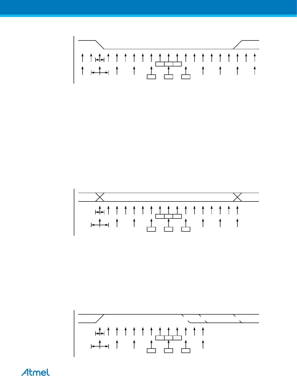
Figure 24-5 Start Bit Sampling
1 2 3 4 5 6 7 8 9 10 11 12 13 14 15 16 1 2
STARTIDLE
00
BIT 0
3
1 2 3 4 5 6 7 8 1 20
RxD
Sample
(U2X = 0)
Sample
(U2X = 1)
When the clock recovery logic detects a high (idle) to low (start) transition on the RxD line, the start bit
detection sequence is initiated. Let sample 1 denote the first zero-sample as shown in the figure. The
clock recovery logic then uses samples 8, 9 and 10 for Normal mode, and samples 4, 5 and 6 for Double
Speed mode (indicated with sample numbers inside boxes on the figure), to decide if a valid start bit is
received. If two or more of these three samples have logical high levels (the majority wins), the start bit is
rejected as a noise spike and the Receiver starts looking for the next high to low-transition. If however, a
valid start bit is detected, the clock recovery logic is synchronized and the data recovery can begin. The
synchronization process is repeated for each start bit.
24.8.2. Asynchronous Data Recovery
When the Receiver clock is synchronized to the start bit, the data recovery can begin. The data recovery
unit uses a state machine that has 16 states for each bit in Normal mode and eight states for each bit in
Double Speed mode. The following figure shows the sampling of the data bits and the parity bit. Each of
the samples is given a number that is equal to the state of the recovery unit.
Figure 24-6 Sampling of Data and Parity Bit
1 2 3 4 5 6 7 8 9 10 11 12 13 14 15 16 1
BIT n
1 2 3 4 5 6 7 8 1
RxD
Sample
(U2X = 0)
Sample
(U2X = 1)
The decision of the logic level of the received bit is taken by doing a majority voting of the logic value to
the three samples in the center of the received bit. The center samples are emphasized on the figure by
having the sample number inside boxes. The majority voting process is done as follows: If two or all three
samples have high levels, the received bit is registered to be a logic 1. If two or all three samples have
low levels, the received bit is registered to be a logic 0. This majority voting process acts as a low pass
filter for the incoming signal on the RxD pin. The recovery process is then repeated until a complete
frame is received. Including the first stop bit. Note that the Receiver only uses the first stop bit of a frame.
The following figure shows the sampling of the stop bit and the earliest possible beginning of the start bit
of the next frame.
Figure 24-7 Stop Bit Sampling and Next Start Bit Sampling
1 2 3 4 5 6 7 8 9 10 0/1 0/1 0/1
STOP 1
1 2 3 4 5 6 0/1
RxD
Sample
(U2X = 0)
Sample
(U2X = 1)
(A) (B) (C)
Atmel ATmega8A [DATASHEET]
Atmel-8159F-8-bit AVR Microcontroller_Datasheet_Complete-09/2015
194
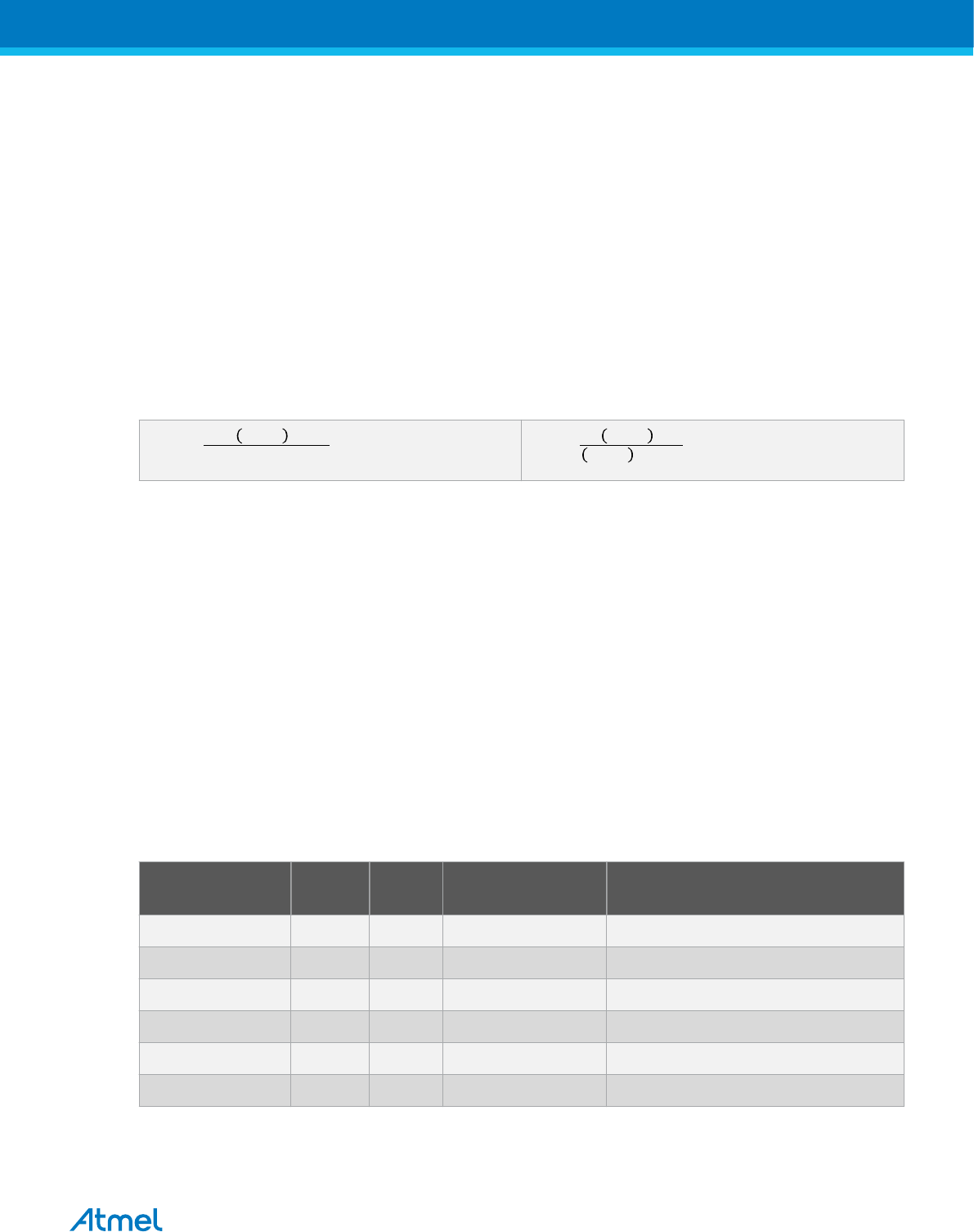
The same majority voting is done to the stop bit as done for the other bits in the frame. If the stop bit is
registered to have a logic 0 value, the Frame Error (FE) Flag will be set.
A new high to low transition indicating the start bit of a new frame can come right after the last of the bits
used for majority voting. For Normal Speed mode, the first low level sample can be at point marked (A) in
the figure above. For Double Speed mode the first low level must be delayed to (B). (C) marks a stop bit
of full length. The early start bit detection influences the operational range of the Receiver.
24.8.3. Asynchronous Operational Range
The operational range of the Receiver is dependent on the mismatch between the received bit rate and
the internally generated baud rate. If the Transmitter is sending frames at too fast or too slow bit rates, or
the internally generated baud rate of the Receiver does not have a similar (refer to next table) base
frequency, the Receiver will not be able to synchronize the frames to the start bit.
The following equations can be used to calculate the ratio of the incoming data rate and internal receiver
baud rate.
slow =+ 1
1+ +
fast =+ 2
+ 1 +
DSum of character size and parity size (D = 5- to 10-bit).
SSamples per bit. S = 16 for Normal Speed mode and S = 8 for Double Speed mode.
SFFirst sample number used for majority voting. SF = 8 for Normal Speed and SF = 4 for Double
Speed mode.
SMMiddle sample number used for majority voting. SM = 9 for Normal Speed and SM = 5 for Double
Speed mode.
Rslow is the ratio of the slowest incoming data rate that can be accepted in relation to the Receiver
baud rate.
Rfast is the ratio of the fastest incoming data rate that can be accepted in relation to the Receiver baud
rate.
The following tables list the maximum receiver baud rate error that can be tolerated. Note that Normal
Speed mode has higher toleration of baud rate variations.
Table 24-2 Recommended Maximum Receiver Baud Rate Error for Normal Speed Mode (U2X = 0)
D
# (Data+Parity Bit)
Rslow [%] Rfast [%] Max. Total Error [%] Recommended Max Receiver Error
[%]
5 93.20 106.67 +6.67/-6.8 ±3.0
6 94.12 105.79 +5.79/-5.88 ±2.5
7 94.81 105.11 +5.11/-5.19 ±2.0
8 95.36 104.58 +4.58/-4.54 ±2.0
9 95.81 104.14 +4.14/-4.19 ±1.5
10 96.17 103.78 +3.78/-3.83 ±1.5
Atmel ATmega8A [DATASHEET]
Atmel-8159F-8-bit AVR Microcontroller_Datasheet_Complete-09/2015
195
Table 24-3 Recommended Maximum Receiver Baud Rate Error for Double Speed Mode (U2X = 1)
D
# (Data+Parity Bit)
Rslow [%] Rfast [%] Max Total Error [%] Recommended Max
Receiver Error [%]
5 94.12 105.66 +5.66/-5.88 ±2.5
6 94.92 104.92 +4.92/-5.08 ±2.0
7 95.52 104.35 +4.35/-4.48 ±1.5
8 96.00 103.90 +3.90/-4.00 ±1.5
9 96.39 103.53 +3.53/-3.61 ±1.5
10 96.70 103.23 +3.23/-3.30 ±1.0
The recommendations of the maximum Receiver baud rate error was made under the assumption that
the Receiver and Transmitter equally divides the maximum total error.
There are two possible sources for the Receivers Baud Rate error. The Receiver’s system clock (XTAL)
will always have some minor instability over the supply voltage range and the temperature range. When
using a crystal to generate the system clock, this is rarely a problem, but for a resonator the system clock
may differ more than 2% depending of the resonators tolerance. The second source for the error is more
controllable. The baud rate generator can not always do an exact division of the system frequency to get
the baud rate wanted. In this case an UBRR value that gives an acceptable low error can be used if
possible.
24.9. Multi-Processor Communication Mode
Setting the Multi-processor Communication mode (MPCM) bit in UCSRA enables a filtering function of
incoming frames received by the USART Receiver. Frames that do not contain address information will
be ignored and not put into the receive buffer. This effectively reduces the number of incoming frames
that has to be handled by the CPU, in a system with multiple MCUs that communicate via the same serial
bus. The Transmitter is unaffected by the MPCM setting, but has to be used differently when it is a part of
a system utilizing the Multi-processor Communication mode.
If the Receiver is set up to receive frames that contain 5 to 8 data bits, then the first stop bit indicates if
the frame contains data or address information. If the Receiver is set up for frames with nine data bits,
then the ninth bit (RXB8) is used for identifying address and data frames. When the frame type bit (the
first stop or the ninth bit) is one, the frame contains an address. When the frame type bit is zero the frame
is a data frame.
The Multi-processor Communication mode enables several Slave MCUs to receive data from a Master
MCU. This is done by first decoding an address frame to find out which MCU has been addressed. If a
particular Slave MCU has been addressed, it will receive the following data frames as normal, while the
other Slave MCUs will ignore the received frames until another address frame is received.
24.9.1. Using MPCM
For an MCU to act as a Master MCU, it can use a 9-bit character frame format (UCSZ = 7). The ninth bit
(TXB8) must be set when an address frame (TXB8 = 1) or cleared when a data frame (TXB = 0) is being
transmitted. The Slave MCUs must in this case be set to use a 9-bit character frame format.
The following procedure should be used to exchange data in Multi-Processor Communication Mode:
1. All Slave MCUs are in Multi-processor Communication mode (MPCM in UCSRA is set).
Atmel ATmega8A [DATASHEET]
Atmel-8159F-8-bit AVR Microcontroller_Datasheet_Complete-09/2015
196

2. The Master MCU sends an address frame, and all slaves receive and read this frame. In the Slave
MCUs, the RXC Flag in UCSRA will be set as normal.
3. Each Slave MCU reads the UDR Register and determines if it has been selected. If so, it clears the
MPCM bit in UCSRA, otherwise it waits for the next address byte and keeps the MPCM setting.
4. The addressed MCU will receive all data frames until a new address frame is received. The other
Slave MCUs, which still have the MPCM bit set, will ignore the data frames.
5. When the last data frame is received by the addressed MCU, the addressed MCU sets the MPCM
bit and waits for a new address frame from Master. The process then repeats from 2.
Using any of the 5- to 8-bit character frame formats is possible, but impractical since the Receiver must
change between using n and n+1 character frame formats. This makes full-duplex operation difficult since
the Transmitter and Receiver uses the same character size setting. If 5- to 8-bit character frames are
used, the Transmitter must be set to use two stop bit (USBS = 1) since the first stop bit is used for
indicating the frame type.
Do not use Read-Modify-Write instructions (SBI and CBI) to set or clear the MPCM bit. The MPCM bit
shares the same I/O location as the TXC Flag and this might accidentally be cleared when using SBI or
CBI instructions.
24.10. Accessing UBRRH/UCSRC Registers
The UBRRH Register shares the same I/O location as the UCSRC Register. Therefore some special
consideration must be taken when accessing this I/O location.
24.10.1. Write Access
When doing a write access of this I/O location, the high bit of the value written, the USART Register
Select (URSEL) bit, controls which one of the two registers that will be written. If URSEL is zero during a
write operation, the UBRRH value will be updated. If URSEL is one, the UCSRC setting will be updated.
The following code examples show how to access the two registers.
Assembly Code Example(1)
:.
; Set UBRRH to 2
ldi r16,0x02
out UBRRH,r16
:.
; Set the USBS and the UCSZ1 bit to one, and
; the remaining bits to zero.
ldi r16,(1<<URSEL) | (1<<USBS) | (1<<UCSZ1)
out UCSRC,r16
:.
C Code Example(1)
:.
/* Set UBRRH to 2 */
UBRRH = 0x02;
:.
/* Set the USBS and the UCSZ1 bit to one, and */
/* the remaining bits to zero. */
UCSRC = (1<<URSEL) | (1<<USBS) | (1<<UCSZ1);
:.
Note: 1. See About Code Examples.
Atmel ATmega8A [DATASHEET]
Atmel-8159F-8-bit AVR Microcontroller_Datasheet_Complete-09/2015
197

As the code examples illustrate, write accesses of the two registers are relatively
unaffected of the sharing of I/O location.
Related Links
About Code Examples on page 23
24.10.2. Read Access
Doing a read access to the UBRRH or the UCSRC Register is a more complex operation. However, in
most applications, it is rarely necessary to read any of these registers.
The read access is controlled by a timed sequence. Reading the I/O location once returns the UBRRH
Register contents. If the register location was read in previous system clock cycle, reading the register in
the current clock cycle will return the UCSRC contents. Note that the timed sequence for reading the
UCSRC is an atomic operation. Interrupts must therefore be controlled (e.g., by disabling interrupts
globally) during the read operation.
The following code example shows how to read the UCSRC Register contents.
Assembly Code Example(1)
USART_ReadUCSRC:
; Read UCSRC
in r16,UBRRH
in r16,UCSRC
ret
C Code Example(1)
unsigned char USART_ReadUCSRC( void )
{
unsigned char ucsrc;
/* Read UCSRC */
ucsrc = UBRRH;
ucsrc = UCSRC;
return ucsrc;
}
Note: 1. See About Code Examples.
The assembly code example returns the UCSRC value in r16.
Reading the UBRRH contents is not an atomic operation and therefore it can be read as
an ordinary register, as long as the previous instruction did not access the register
location.
Related Links
About Code Examples on page 23
24.11. Register Description
Atmel ATmega8A [DATASHEET]
Atmel-8159F-8-bit AVR Microcontroller_Datasheet_Complete-09/2015
198

24.11.1. UDR – USART I/O Data Register
When using the I/O specific commands IN and OUT, the I/O addresses 0x00 - 0x3F must be used. When
addressing I/O Registers as data space using LD and ST instructions, 0x20 must be added to these offset
addresses. The device is a complex microcontroller with more peripheral units than can be supported
within the 64 location reserved in Opcode for the IN and OUT instructions. For the Extended I/O space
from 0x60 in SRAM, only the ST/STS/STD and LD/LDS/LDD instructions can be used.
Name: UDR
Offset: 0x0C
Reset: 0x00
Property:
When addressing I/O Registers as data space the offset address is 0x2C
Bit 7 6 5 4 3 2 1 0
TXB / RXB[7:0]
Access R/W R/W R/W R/W R/W R/W R/W R/W
Reset 0 0 0 0 0 0 0 0
Bits 7:0 – TXB / RXB[7:0]: USART Transmit / Receive Data Buffer
The USART Transmit Data Buffer Register and USART Receive Data Buffer Registers share the same
I/O address referred to as USART Data Register or UDR. The Transmit Data Buffer Register (TXB) will be
the destination for data written to the UDR Register location. Reading the UDR Register location will
return the contents of the Receive Data Buffer Register (RXB).
For 5-, 6-, or 7-bit characters the upper unused bits will be ignored by the Transmitter and set to zero by
the Receiver.
The transmit buffer can only be written when the UDRE Flag in the UCSRA Register is set. Data written
to UDR when the UDRE Flag is not set, will be ignored by the USART Transmitter. When data is written
to the transmit buffer, and the Transmitter is enabled, the Transmitter will load the data into the Transmit
Shift Register when the Shift Register is empty. Then the data will be serially transmitted on the TxD pin.
The receive buffer consists of a two level FIFO. The FIFO will change its state whenever the receive
buffer is accessed. Due to this behavior of the receive buffer, do not use Read-Modify-Write instructions
(SBI and CBI) on this location. Be careful when using bit test instructions (SBIC and SBIS), since these
also will change the state of the FIFO.
Atmel ATmega8A [DATASHEET]
Atmel-8159F-8-bit AVR Microcontroller_Datasheet_Complete-09/2015
199

24.11.2. UCSRA – USART Control and Status Register A
When using the I/O specific commands IN and OUT, the I/O addresses 0x00 - 0x3F must be used. When
addressing I/O Registers as data space using LD and ST instructions, 0x20 must be added to these offset
addresses. The device is a complex microcontroller with more peripheral units than can be supported
within the 64 location reserved in Opcode for the IN and OUT instructions. For the Extended I/O space
from 0x60 in SRAM, only the ST/STS/STD and LD/LDS/LDD instructions can be used.
Name: UCSRA
Offset: 0x0B
Reset: 0x20
Property:
When addressing I/O Registers as data space the offset address is 0x2B
Bit 7 6 5 4 3 2 1 0
RXC TXC UDRE FE DOR PE U2X MPCM
Access R R/W R R R R R/W R/W
Reset 0 0 1 0 0 0 0 0
Bit 7 – RXC: USART Receive Complete
This flag bit is set when there are unread data in the receive buffer and cleared when the receive buffer is
empty (i.e. does not contain any unread data). If the Receiver is disabled, the receive buffer will be
flushed and consequently the RXC bit will become zero. The RXC Flag can be used to generate a
Receive Complete interrupt (see description of the RXCIE bit).
Bit 6 – TXC: USART Transmit Complete
This flag bit is set when the entire frame in the Transmit Shift Register has been shifted out and there are
no new data currently present in the transmit buffer (UDR). The TXC Flag bit is automatically cleared
when a transmit complete interrupt is executed, or it can be cleared by writing a one to its bit location. The
TXC Flag can generate a Transmit Complete interrupt (see description of the TXCIE bit).
Bit 5 – UDRE: USART Data Register Empty
The UDRE Flag indicates if the transmit buffer (UDR) is ready to receive new data. If UDRE is one, the
buffer is empty, and therefore ready to be written. The UDRE Flag can generate a Data Register Empty
interrupt (see description of the UDRIE bit).
UDRE is set after a reset to indicate that the Transmitter is ready.
Bit 4 – FE: Frame Error
This bit is set if the next character in the receive buffer had a Frame Error when received (i.e., when the
first stop bit of the next character in the receive buffer is zero). This bit is valid until the receive buffer
(UDR) is read. The FE bit is zero when the stop bit of received data is one. Always set this bit to zero
when writing to UCSRA.
Bit 3 – DOR: Data OverRun
This bit is set if a Data OverRun condition is detected. A Data OverRun occurs when the receive buffer is
full (two characters), it is a new character waiting in the Receive Shift Register, and a new start bit is
detected. This bit is valid until the receive buffer (UDR) is read. Always set this bit to zero when writing to
UCSRA.
Atmel ATmega8A [DATASHEET]
Atmel-8159F-8-bit AVR Microcontroller_Datasheet_Complete-09/2015
200

Bit 2 – PE: Parity Error
This bit is set if the next character in the receive buffer had a Parity Error when received and the parity
checking was enabled at that point (UPM1 = 1). This bit is valid until the receive buffer (UDR) is read.
Always set this bit to zero when writing to UCSRA.
Bit 1 – U2X: Double the USART Transmission Speed
This bit only has effect for the asynchronous operation. Write this bit to zero when using synchronous
operation.
Writing this bit to one will reduce the divisor of the baud rate divider from 16 to 8 effectively doubling the
transfer rate for asynchronous communication.
Bit 0 – MPCM: Multi-processor Communication Mode
This bit enables the Multi-processor Communication mode. When the MPCM bit is written to one, all the
incoming frames received by the USART Receiver that do not contain address information will be
ignored. The Transmitter is unaffected by the MPCM setting. For more detailed information see Multi-
processor Communication Mode.
Atmel ATmega8A [DATASHEET]
Atmel-8159F-8-bit AVR Microcontroller_Datasheet_Complete-09/2015
201

24.11.3. UCSRB – USART Control and Status Register B
When using the I/O specific commands IN and OUT, the I/O addresses 0x00 - 0x3F must be used. When
addressing I/O Registers as data space using LD and ST instructions, 0x20 must be added to these offset
addresses. The device is a complex microcontroller with more peripheral units than can be supported
within the 64 location reserved in Opcode for the IN and OUT instructions. For the Extended I/O space
from 0x60 in SRAM, only the ST/STS/STD and LD/LDS/LDD instructions can be used.
Name: UCSRB
Offset: 0x0A
Reset: 0x00
Property:
When addressing I/O Registers as data space the offset address is 0x2A
Bit 7 6 5 4 3 2 1 0
RXCIE TXCIE UDRIE RXEN TXEN UCSZ2 RXB8 TXB8
Access R/W R/W R/W R/W R/W R/W R R/W
Reset 0 0 0 0 0 0 0 0
Bit 7 – RXCIE: RX Complete Interrupt Enable
Writing this bit to one enables interrupt on the RXC Flag. A USART Receive Complete interrupt will be
generated only if the RXCIE bit is written to one, the Global Interrupt Flag in SREG is written to one and
the RXC bit in UCSRA is set.
Bit 6 – TXCIE: TX Complete Interrupt Enable
Writing this bit to one enables interrupt on the TXC Flag. A USART Transmit Complete interrupt will be
generated only if the TXCIE bit is written to one, the Global Interrupt Flag in SREG is written to one and
the TXC bit in UCSRA is set.
Bit 5 – UDRIE: USART Data Register Empty Interrupt Enable
Writing this bit to one enables interrupt on the UDRE Flag. A Data Register Empty interrupt will be
generated only if the UDRIE bit is written to one, the Global Interrupt Flag in SREG is written to one and
the UDRE bit in UCSRA is set.
Bit 4 – RXEN: Receiver Enable
Writing this bit to one enables the USART Receiver. The Receiver will override normal port operation for
the RxD pin when enabled. Disabling the Receiver will flush the receive buffer invalidating the FE, DOR
and PE Flags.
Bit 3 – TXEN: Transmitter Enable
Writing this bit to one enables the USART Transmitter. The Transmitter will override normal port operation
for the TxD pin when enabled. The disabling of the Transmitter (writing TXEN to zero) will not become
effective until ongoing and pending transmissions are completed (i.e., when the Transmit Shift Register
and Transmit Buffer Register do not contain data to be transmitted). When disabled, the Transmitter will
no longer override the TxD port.
Bit 2 – UCSZ2: Character Size
The UCSZ2 bits combined with the UCSZ1:0 bit in UCSRC sets the number of data bits (Character Size)
in a frame the Receiver and Transmitter use.
Atmel ATmega8A [DATASHEET]
Atmel-8159F-8-bit AVR Microcontroller_Datasheet_Complete-09/2015
202

Bit 1 – RXB8: Receive Data Bit 8
RXB8 is the ninth data bit of the received character when operating with serial frames with nine data bits.
Must be read before reading the low bits from UDR.
Bit 0 – TXB8: Transmit Data Bit 8
TXB8 is the ninth data bit in the character to be transmitted when operating with serial frames with nine
data bits. Must be written before writing the low bits to UDR.
Atmel ATmega8A [DATASHEET]
Atmel-8159F-8-bit AVR Microcontroller_Datasheet_Complete-09/2015
203
24.11.4. UCSRC – USART Control and Status Register C
When using the I/O specific commands IN and OUT, the I/O addresses 0x00 - 0x3F must be used. When
addressing I/O Registers as data space using LD and ST instructions, 0x20 must be added to these offset
addresses. The device is a complex microcontroller with more peripheral units than can be supported
within the 64 location reserved in Opcode for the IN and OUT instructions. For the Extended I/O space
from 0x60 in SRAM, only the ST/STS/STD and LD/LDS/LDD instructions can be used.
The UCSRC Register shares the same I/O location as the UBRRH Register. See the Accessing UBRRH/
UCSRC Registers section which describes how to access this register.
Name: UCSRC
Offset: 0x20
Reset: 0x06
Property:
When addressing I/O Registers as data space the offset address is 0x40
Bit 7 6 5 4 3 2 1 0
URSEL UMSEL UPM1 UPM0 USBS UCSZ1 UCSZ0 UCPOL
Access R/W R/W R/W R/W R/W R/W R/W R/W
Reset 1 0 0 0 0 0 1 0
Bit 7 – URSEL: Register Select
This bit selects between accessing the UCSRC or the UBRRH Register. It is read as one when reading
UCSRC. The URSEL must be one when writing the UCSRC.
Bit 6 – UMSEL: Mode Select
This bit selects between Asynchronous and Synchronous mode of operation.
Table 24-4 UMSEL Bit Settings
UMSEL Bit Settings Mode
0 Asynchronous Operation
1 Synchronous Operation
Bits 5:4 – UPMn: Parity Mode [n = 1:0]
These bits enable and set type of Parity Generation and Check. If enabled, the Transmitter will
automatically generate and send the parity of the transmitted data bits within each frame. The Receiver
will generate a parity value for the incoming data and compare it to the UPM0 setting. If a mismatch is
detected, the PE Flag in UCSRA will be set.
Table 24-5 UPM Bits Settings
UPM1 UPM0 ParityMode
0 0 Disabled
0 1 Reserved
1 0 Enabled, Even Parity
1 1 Enabled, Odd Parity
Atmel ATmega8A [DATASHEET]
Atmel-8159F-8-bit AVR Microcontroller_Datasheet_Complete-09/2015
204

Bit 3 – USBS: Stop Bit Select
This bit selects the number of stop bits to be inserted by the Transmitter. The Receiver ignores this
setting.
Table 24-6 USBS Bit Settings
USBS Stop Bit(s)
0 1-bit
1 2-bit
Bits 2:1 – UCSZn: Character Size [n = 1:0]
The UCSZ1:0 bits combined with the UCSZ2 bit in UCSRB sets the number of data bits (Character Size)
in a frame the Receiver and Transmitter use.
Table 24-7 UCSZ Bits Settings
UCSZ2 UCSZ1 UCSZ0 Character Size
0 0 0 5-bit
0 0 1 6-bit
0 1 0 7-bit
0 1 1 8-bit
1 0 0 Reserved
1 0 1 Reserved
1 1 0 Reserved
1 1 1 9-bit
Bit 0 – UCPOL: Clock Polarity
This bit is used for Synchronous mode only. Write this bit to zero when Asynchronous mode is used. The
UCPOL bit sets the relationship between data output change and data input sample, and the
synchronous clock (XCK).
Table 24-8 UCPOL Bit Settings
UCPOL Transmitted Data Changed (Output of TxD
Pin)
Received Data Sampled (Input on RxD
Pin)
0 Rising XCK Edge Falling XCK Edge
1 Falling XCK Edge Rising XCK Edge
Atmel ATmega8A [DATASHEET]
Atmel-8159F-8-bit AVR Microcontroller_Datasheet_Complete-09/2015
205

24.11.5. UBRRL – USART Baud Rate Register Low
When using the I/O specific commands IN and OUT, the I/O addresses 0x00 - 0x3F must be used. When
addressing I/O Registers as data space using LD and ST instructions, 0x20 must be added to these offset
addresses. The device is a complex microcontroller with more peripheral units than can be supported
within the 64 location reserved in Opcode for the IN and OUT instructions. For the Extended I/O space
from 0x60 in SRAM, only the ST/STS/STD and LD/LDS/LDD instructions can be used.
Name: UBRRL
Offset: 0x09
Reset: 0x00
Property:
When addressing I/O Registers as data space the offset address is 0x29
Bit 7 6 5 4 3 2 1 0
UBBR[7:0]
Access R/W R/W R/W R/W R/W R/W R/W R/W
Reset 0 0 0 0 0 0 0 0
Bits 7:0 – UBBR[7:0]: USART Baud Rate Register
This is a 12-bit register which contains the USART baud rate. The UBRRH contains the four most
significant bits, and the UBRRL contains the eight least significant bits of the USART baud rate. Ongoing
transmissions by the Transmitter and Receiver will be corrupted if the baud rate is changed. Writing
UBRRL will trigger an immediate update of the baud rate prescaler.
Atmel ATmega8A [DATASHEET]
Atmel-8159F-8-bit AVR Microcontroller_Datasheet_Complete-09/2015
206
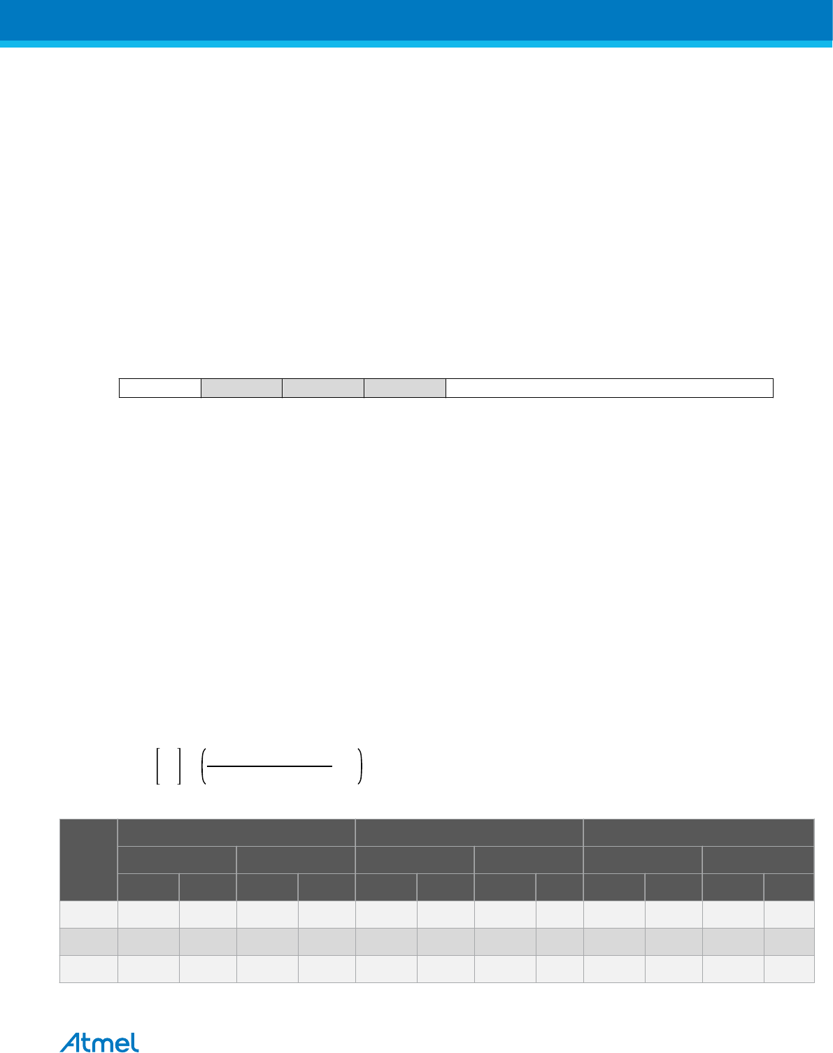
24.11.6. UBBRH – USART Baud Rate Register High
When using the I/O specific commands IN and OUT, the I/O addresses 0x00 - 0x3F must be used. When
addressing I/O Registers as data space using LD and ST instructions, 0x20 must be added to these offset
addresses. The device is a complex microcontroller with more peripheral units than can be supported
within the 64 location reserved in Opcode for the IN and OUT instructions. For the Extended I/O space
from 0x60 in SRAM, only the ST/STS/STD and LD/LDS/LDD instructions can be used.
The UBRRH Register shares the same I/O location as the UCSRC Register. See the Accessing UBRRH/
UCSRC Registers section which describes how to access this register.
Name: UBBRH
Offset: 0x20
Reset: 0x00
Property:
When addressing I/O Registers as data space the offset address is 0x40
Bit 7 6 5 4 3 2 1 0
URSEL UBRR[3:0]
Access R/W R/W R/W R/W R/W
Reset 0 0 0 0 0
Bit 7 – URSEL: Register Select
This bit selects between accessing the UBRRH or the UCSRC Register. It is read as zero when reading
UBRRH. The URSEL must be zero when writing the UBRRH.
Bits 3:0 – UBRR[3:0]: USART Baud Rate Register [n = 11:8]
Refer to UBRRL.
24.12. Examples of Baud Rate Setting
For standard crystal and resonator frequencies, the most commonly used baud rates for asynchronous
operation can be generated by using the UBRR settings as listed in the table below.
UBRR values which yield an actual baud rate differing less than 0.5% from the target baud rate, are bold
in the table. Higher error ratings are acceptable, but the Receiver will have less noise resistance when the
error ratings are high, especially for large serial frames (see Asynchronous Operational Range). The error
values are calculated using the following equation:
% = BaudRateClosest Match
BaudRate 1× 100 %
Table 24-9 Examples of UBRR Settings for Commonly Used Oscillator Frequencies
Baud
Rate
[bps]
fosc = 1.0000MHz fosc = 1.8432MHz fosc = 2.0000MHz
U2X = 0 U2X = 1 U2X= 0 U2X = 1 U2X = 0 U2X = 1
UBRR Error UBRR Error UBRR Error UBRR Error UBRR Error UBRR Error
2400 25 0.2% 51 0.2% 47 0.0% 95 0.0% 51 0.2% 103 0.2%
4800 12 0.2% 25 0.2% 23 0.0% 47 0.0% 25 0.2% 51 0.2%
9600 6 -7.0% 12 0.2% 11 0.0% 23 0.0% 12 0.2% 25 0.2%
Atmel ATmega8A [DATASHEET]
Atmel-8159F-8-bit AVR Microcontroller_Datasheet_Complete-09/2015
207
Baud
Rate
[bps]
fosc = 1.0000MHz fosc = 1.8432MHz fosc = 2.0000MHz
U2X = 0 U2X = 1 U2X= 0 U2X = 1 U2X = 0 U2X = 1
UBRR Error UBRR Error UBRR Error UBRR Error UBRR Error UBRR Error
14.4k 3 8.5% 8 -3.5% 7 0.0% 15 0.0% 8 -3.5% 16 2.1%
19.2k 2 8.5% 6 -7.0% 5 0.0% 11 0.0% 6 -7.0% 12 0.2%
28.8k 1 8.5% 3 8.5% 3 0.0% 7 0.0% 3 8.5% 8 -3.5%
38.4k 1 -18.6% 2 8.5% 2 0.0% 5 0.0% 2 8.5% 6 -7.0%
57.6k 0 8.5% 1 8.5% 1 0.0% 3 0.0% 1 8.5% 3 8.5%
76.8k – – 1 -18.6% 1 -25.0% 2 0.0% 1 -18.6% 2 8.5%
115.2k – – 0 8.5% 0 0.0% 1 0.0% 0 8.5% 1 8.5%
230.4k – – – – – – 0 0.0% – – – –
250k – – – – – – – – – – 0 0.0%
Max(1) 62.5kbps 125kbps 115.2kbps 230.4kbps 125kbps 250kbps
Note: 1. UBRR = 0, Error = 0.0%
Table 24-10 Examples of UBRR Settings for Commonly Used Oscillator Frequencies (Continued)
Baud
Rate
[bps]
fosc = 3.6864MHz fosc = 4.0000MHz fosc = 7.3728MHz
U2X = 0 U2X = 1 U2X = 0 U2X = 1 U2X = 0 U2X = 1
UBRR Error UBRR Error UBRR Error UBRR Error UBRR Error UBRR Error
2400 95 0.0% 191 0.0% 103 0.2% 207 0.2% 191 0.0% 383 0.0%
4800 47 0.0% 95 0.0% 51 0.2% 103 0.2% 95 0.0% 191 0.0%
9600 23 0.0% 47 0.0% 25 0.2% 51 0.2% 47 0.0% 95 0.0%
14.4k 15 0.0% 31 0.0% 16 2.1% 34 -0.8% 31 0.0% 63 0.0%
19.2k 11 0.0% 23 0.0% 12 0.2% 25 0.2% 23 0.0% 47 0.0%
28.8k 7 0.0% 15 0.0% 8 -3.5% 16 2.1% 15 0.0% 31 0.0%
38.4k 5 0.0% 11 0.0% 6 -7.0% 12 0.2% 11 0.0% 23 0.0%
57.6k 3 0.0% 7 0.0% 3 8.5% 8 -3.5% 7 0.0% 15 0.0%
76.8k 2 0.0% 5 0.0% 2 8.5% 6 -7.0% 5 0.0% 11 0.0%
115.2k 1 0.0% 3 0.0% 1 8.5% 3 8.5% 3 0.0% 7 0.0%
230.4k 0 0.0% 1 0.0% 0 8.5% 1 8.5% 1 0.0% 3 0.0%
250k 0 -7.8% 1 -7.8% 0 0.0% 1 0.0% 1 -7.8% 3 -7.8%
0.5M – – 0 -7.8% – – 0 0.0% 0 -7.8% 1 -7.8%
1M – – – – – – – – – – 0 -7.8%
Max.(1) 230.4kbps 460.8kbps 250kbps 0.5Mbps 460.8kbps 921.6kbps
Atmel ATmega8A [DATASHEET]
Atmel-8159F-8-bit AVR Microcontroller_Datasheet_Complete-09/2015
208
Note: 1. UBRR = 0, Error = 0.0%
Table 24-11 Examples of UBRR Settings for Commonly Used Oscillator Frequencies (Continued)
Baud
Rate
[bps]
fosc = 8.0000MHz fosc = 11.0592MHz fosc = 14.7456MHz
U2X = 0 U2X = 1 U2X = 0 U2X = 1 U2X = 0 U2X = 1
UBRR Error UBRR Error UBRR Error UBRR Error UBRR Error UBRR Error
2400 207 0.2% 416 -0.1% 287 0.0% 575 0.0% 383 0.0% 767 0.0%
4800 103 0.2% 207 0.2% 143 0.0% 287 0.0% 191 0.0% 383 0.0%
9600 51 0.2% 103 0.2% 71 0.0% 143 0.0% 95 0.0% 191 0.0%
14.4k 34 -0.8% 68 0.6% 47 0.0% 95 0.0% 63 0.0% 127 0.0%
19.2k 25 0.2% 51 0.2% 35 0.0% 71 0.0% 47 0.0% 95 0.0%
28.8k 16 2.1% 34 -0.8% 23 0.0% 47 0.0% 31 0.0% 63 0.0%
38.4k 12 0.2% 25 0.2% 17 0.0% 35 0.0% 23 0.0% 47 0.0%
57.6k 8 -3.5% 16 2.1% 11 0.0% 23 0.0% 15 0.0% 31 0.0%
76.8k 6 -7.0% 12 0.2% 8 0.0% 17 0.0% 11 0.0% 23 0.0%
115.2k 3 8.5% 8 -3.5% 5 0.0% 11 0.0% 7 0.0% 15 0.0%
230.4k 1 8.5% 3 8.5% 2 0.0% 5 0.0% 3 0.0% 7 0.0%
250k 1 0.0% 3 0.0% 2 -7.8% 5 -7.8% 3 -7.8% 6 5.3%
0.5M 0 0.0% 1 0.0% – – 2 -7.8% 1 -7.8% 3 -7.8%
1M – – 0 0.0% – – – – 0 -7.8% 1 -7.8%
Max.(1) 0.5Mbps 1Mbps 691.2kbps 1.3824Mbps 921.6kbps 1.8432Mbps
Note: 1. UBRR = 0, Error = 0.0%
Table 24-12 Examples of UBRR Settings for Commonly Used Oscillator Frequencies (Continued)
Baud
Rate
[bps]
fosc = 16.0000MHz fosc = 18.4320MHz fosc = 20.0000MHz
U2X = 0 U2X = 1 U2X = 0 U2X = 1 U2X = 0 U2X = 1
UBRR Error UBRR Error UBRR Error UBRR Error UBRR Error UBRR Error
2400 416 -0.1% 832 0.0% 479 0.0% 959 0.0% 520 0.0% 1041 0.0%
4800 207 0.2% 416 -0.1% 239 0.0% 479 0.0% 259 0.2% 520 0.0%
9600 103 0.2% 207 0.2% 119 0.0% 239 0.0% 129 0.2% 259 0.2%
14.4k 68 0.6% 138 -0.1% 79 0.0% 159 0.0% 86 -0.2% 173 -0.2%
19.2k 51 0.2% 103 0.2% 59 0.0% 119 0.0% 64 0.2% 129 0.2%
28.8k 34 -0.8% 68 0.6% 39 0.0% 79 0.0% 42 0.9% 86 -0.2%
38.4k 25 0.2% 51 0.2% 29 0.0% 59 0.0% 32 -1.4% 64 0.2%
Atmel ATmega8A [DATASHEET]
Atmel-8159F-8-bit AVR Microcontroller_Datasheet_Complete-09/2015
209

Baud
Rate
[bps]
fosc = 16.0000MHz fosc = 18.4320MHz fosc = 20.0000MHz
U2X = 0 U2X = 1 U2X = 0 U2X = 1 U2X = 0 U2X = 1
UBRR Error UBRR Error UBRR Error UBRR Error UBRR Error UBRR Error
57.6k 16 2.1% 34 -0.8% 19 0.0% 39 0.0% 21 -1.4% 42 0.9%
76.8k 12 0.2% 25 0.2% 14 0.0% 29 0.0% 15 1.7% 32 -1.4%
115.2k 8 -3.5% 16 2.1% 9 0.0% 19 0.0% 10 -1.4% 21 -1.4%
230.4k 3 8.5% 8 -3.5% 4 0.0% 9 0.0% 4 8.5% 10 -1.4%
250k 3 0.0% 7 0.0% 4 -7.8% 8 2.4% 4 0.0% 9 0.0%
0.5M 1 0.0% 3 0.0% – – 4 -7.8% – – 4 0.0%
1M 0 0.0% 1 0.0% – – – – – – – –
Max.(1) 1Mbps 2Mbps 1.152Mbps 2.304Mbps 1.25Mbps 2.5Mbps
Note: 1. UBRR = 0, Error = 0.0%
Atmel ATmega8A [DATASHEET]
Atmel-8159F-8-bit AVR Microcontroller_Datasheet_Complete-09/2015
210
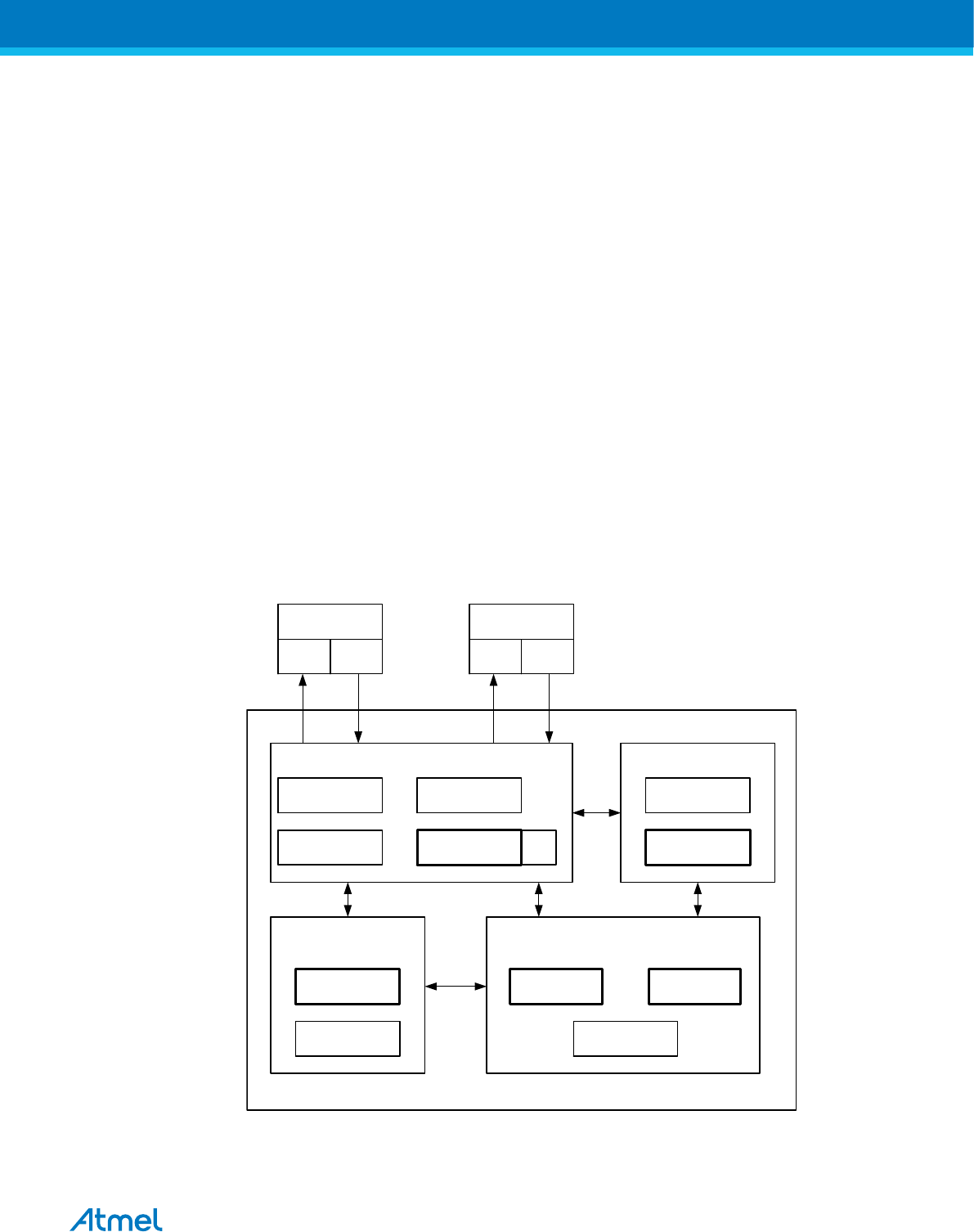
25. TWI - Two-wire Serial Interface
25.1. Features
•Simple, yet Powerful and Flexible Communication Interface, only two Bus Lines Needed
•Both Master and Slave Operation Supported
•Device can Operate as Transmitter or Receiver
•7-bit Address Space Allows up to 128 Different Slave Addresses
•Multi-master Arbitration Support
•Up to 400kHz Data Transfer Speed
•Slew-rate Limited Output Drivers
•Noise Suppression Circuitry Rejects Spikes on Bus Lines
•Fully Programmable Slave Address with General Call Support
•Address Recognition Causes Wake-up When AVR is in Sleep Mode
25.2. Overview
The TWI module is comprised of several submodules, as shown in the following figure. All registers
drawn in a thick line are accessible through the AVR data bus.
Figure 25-1 Overview of the TWI Module
TWI Unit
Address Register
(TW AR)
Address Match Unit
Address Compar ator
Control Unit
Control Register
(TWCR)
Status Register
(TWSR)
State Machine and
Status control
SCL
Sle w-r ate
Control
Spik e
Filter
SD A
Sle w-r ate
Control
Spik e
Filter
Bit Rate Gener ator
Bit Rate Register
(TWBR)
Prescaler
Bus Interf ace Unit
ST AR T / ST OP
Control
Arbitration detection Ack
Spik e Suppression
Address/Data Shift
Register (TWDR)
Atmel ATmega8A [DATASHEET]
Atmel-8159F-8-bit AVR Microcontroller_Datasheet_Complete-09/2015
211

25.2.1. SCL and SDA Pins
These pins interface the AVR TWI with the rest of the MCU system. The output drivers contain a slew-
rate limiter in order to conform to the TWI specification. The input stages contain a spike suppression unit
removing spikes shorter than 50 ns. Note that the internal pull-ups in the AVR pads can be enabled by
setting the PORT bits corresponding to the SCL and SDA pins, as explained in the I/O Port section. The
internal pull-ups can in some systems eliminate the need for external ones.
25.2.2. Bit Rate Generator Unit
This unit controls the period of SCL when operating in a Master mode. The SCL period is controlled by
settings in the TWI Bit Rate Register (TWBR) and the Prescaler bits in the TWI Status Register (TWSR).
Slave operation does not depend on Bit Rate or Prescaler settings, but the CPU clock frequency in the
Slave must be at least 16 times higher than the SCL frequency. Note that slaves may prolong the SCL
low period, thereby reducing the average TWI bus clock period.
The SCL frequency is generated according to the following equation:
SCL frequency = CPU Clock frequency
16 + 2(TWBR) PrescalerValue
•TWBR = Value of the TWI Bit Rate Register
•PrescalerValue = Value of the prescaler, see description of the TWI Prescaler bit in the TWSR
Status Register description (TWSR.TWPS)
Note: Pull-up resistor values should be selected according to the SCL frequency and the capacitive bus
line load. See the Two-Wire Serial Interface Characteristics for a suitable value of the pull-up resistor.
Related Links
Two-wire Serial Interface Characteristics on page 306
25.2.3. Bus Interface Unit
This unit contains the Data and Address Shift Register (TWDR), a START/STOP Controller and
Arbitration detection hardware. The TWDR contains the address or data bytes to be transmitted, or the
address or data bytes received. In addition to the 8-bit TWDR, the Bus Interface Unit also contains a
register containing the (N)ACK bit to be transmitted or received. This (N)ACK Register is not directly
accessible by the application software. However, when receiving, it can be set or cleared by manipulating
the TWI Control Register (TWCR). When in Transmitter mode, the value of the received (N)ACK bit can
be determined by the value in the TWSR.
The START/STOP Controller is responsible for generation and detection of START, REPEATED START,
and STOP conditions. The START/STOP controller is able to detect START and STOP conditions even
when the AVR MCU is in one of the sleep modes, enabling the MCU to wake up if addressed by a Master.
If the TWI has initiated a transmission as Master, the Arbitration Detection hardware continuously
monitors the transmission trying to determine if arbitration is in process. If the TWI has lost an arbitration,
the Control Unit is informed. Correct action can then be taken and appropriate status codes generated.
25.2.4. Address Match Unit
The Address Match unit checks if received address bytes match the seven-bit address in the TWI
Address Register (TWAR). If the TWI General Call Recognition Enable (TWGCE) bit in the TWAR is
written to one, all incoming address bits will also be compared against the General Call address. Upon an
address match, the Control Unit is informed, allowing correct action to be taken. The TWI may or may not
acknowledge its address, depending on settings in the TWCR. The Address Match unit is able to
compare addresses even when the AVR MCU is in sleep mode, enabling the MCU to wake up if
addressed by a Master. If another interrupt (e.g., INT0) occurs during TWI Power-down address match
Atmel ATmega8A [DATASHEET]
Atmel-8159F-8-bit AVR Microcontroller_Datasheet_Complete-09/2015
212
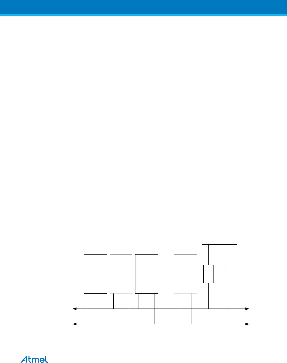
and wakes up the CPU, the TWI aborts operation and return to it’s idle state. If this cause any problems,
ensure that TWI Address Match is the only enabled interrupt when entering Power-down.
25.2.5. Control Unit
The Control unit monitors the TWI bus and generates responses corresponding to settings in the TWI
Control Register (TWCR). When an event requiring the attention of the application occurs on the TWI
bus, the TWI Interrupt Flag (TWINT) is asserted. In the next clock cycle, the TWI Status Register (TWSR)
is updated with a status code identifying the event. The TWSR only contains relevant status information
when the TWI Interrupt Flag is asserted. At all other times, the TWSR contains a special status code
indicating that no relevant status information is available. As long as the TWINT Flag is set, the SCL line
is held low. This allows the application software to complete its tasks before allowing the TWI
transmission to continue.
The TWINT Flag is set in the following situations:
•After the TWI has transmitted a START/REPEATED START condition.
•After the TWI has transmitted SLA+R/W.
•After the TWI has transmitted an address byte.
•After the TWI has lost arbitration.
•After the TWI has been addressed by own slave address or general call.
•After the TWI has received a data byte.
•After a STOP or REPEATED START has been received while still addressed as a Slave.
•When a bus error has occurred due to an illegal START or STOP condition.
25.3. Two-Wire Serial Interface Bus Definition
The Two-wire Serial Interface (TWI) is ideally suited for typical microcontroller applications. The TWI
protocol allows the systems designer to interconnect up to 128 different devices using only two bi-
directional bus lines, one for clock (SCL) and one for data (SDA). The only external hardware needed to
implement the bus is a single pullup resistor for each of the TWI bus lines. All devices connected to the
bus have individual addresses, and mechanisms for resolving bus contention are inherent in the TWI
protocol.
Figure 25-2 TWI Bus Interconnection
SD A
SCL
........ R1 R2
VCC
Device 1 Device 2 Device 3 Device n
25.3.1. TWI Terminology
The following definitions are frequently encountered in this section.
Atmel ATmega8A [DATASHEET]
Atmel-8159F-8-bit AVR Microcontroller_Datasheet_Complete-09/2015
213
Table 25-1 TWI Terminology
Term Description
Master The device that initiates and terminates a transmission. The Master also generates the SCL clock.
Slave The device addressed by a Master.
Transmitter The device placing data on the bus.
Receiver The device reading data from the bus.
25.3.2. Electrical Interconnection
As depicted in Figure 25-2 TWI Bus Interconnection on page 213, both bus lines are connected to the
positive supply voltage through pull-up resistors. The bus drivers of all TWI-compliant devices are open-
drain or open-collector. This implements a wired-AND function which is essential to the operation of the
interface. A low level on a TWI bus line is generated when one or more TWI devices output a zero. A high
level is output when all TWI devices tri-state their outputs, allowing the pull-up resistors to pull the line
high. Note that all AVR devices connected to the TWI bus must be powered in order to allow any bus
operation.
The number of devices that can be connected to the bus is only limited by the bus capacitance limit of
400pF and the 7-bit slave address space. A detailed specification of the electrical characteristics of the
TWI is given in Two-wire Serial Interface Characteristics. Two different sets of specifications are
presented there, one relevant for bus speeds below 100kHz, and one valid for bus speeds up to 400kHz.
Related Links
Two-wire Serial Interface Characteristics on page 306
25.4. Data Transfer and Frame Format
25.4.1. Transferring Bits
Each data bit transferred on the TWI bus is accompanied by a pulse on the clock line. The level of the
data line must be stable when the clock line is high. The only exception to this rule is for generating start
and stop conditions.
Figure 25-3 Data Validity
SD
A
SCL
Data Stab le Data Stab le
Data Change
25.4.2. START and STOP Conditions
The Master initiates and terminates a data transmission. The transmission is initiated when the Master
issues a START condition on the bus, and it is terminated when the Master issues a STOP condition.
Between a START and a STOP condition, the bus is considered busy, and no other master should try to
Atmel ATmega8A [DATASHEET]
Atmel-8159F-8-bit AVR Microcontroller_Datasheet_Complete-09/2015
214
seize control of the bus. A special case occurs when a new START condition is issued between a START
and STOP condition. This is referred to as a REPEATED START condition, and is used when the Master
wishes to initiate a new transfer without relinquishing control of the bus. After a REPEATED START, the
bus is considered busy until the next STOP. This is identical to the START behavior, and therefore START
is used to describe both START and REPEATED START for the remainder of this datasheet, unless
otherwise noted. As depicted below, START and STOP conditions are signalled by changing the level of
the SDA line when the SCL line is high.
Figure 25-4 START, REPEATED START and STOP conditions
SDA
SCL
START STOPREPEATED STARTSTOP START
25.4.3. Address Packet Format
All address packets transmitted on the TWI bus are 9 bits long, consisting of 7 address bits, one READ/
WRITE control bit and an acknowledge bit. If the READ/WRITE bit is set, a read operation is to be
performed, otherwise a write operation should be performed. When a Slave recognizes that it is being
addressed, it should acknowledge by pulling SDA low in the ninth SCL (ACK) cycle. If the addressed
Slave is busy, or for some other reason can not service the Master’s request, the SDA line should be left
high in the ACK clock cycle. The Master can then transmit a STOP condition, or a REPEATED START
condition to initiate a new transmission. An address packet consisting of a slave address and a READ or
a WRITE bit is called SLA+R or SLA+W, respectively.
The MSB of the address byte is transmitted first. Slave addresses can freely be allocated by the designer,
but the address 0000 000 is reserved for a general call.
When a general call is issued, all slaves should respond by pulling the SDA line low in the ACK cycle. A
general call is used when a Master wishes to transmit the same message to several slaves in the system.
When the general call address followed by a Write bit is transmitted on the bus, all slaves set up to
acknowledge the general call will pull the SDA line low in the ack cycle. The following data packets will
then be received by all the slaves that acknowledged the general call. Note that transmitting the general
call address followed by a Read bit is meaningless, as this would cause contention if several slaves
started transmitting different data.
All addresses of the format 1111 xxx should be reserved for future purposes.
Figure 25-5 Address Packet Format
SD A
SCL
ST AR T
1 2 7 8 9
Addr MSB Addr LSB R/W ACK
Atmel ATmega8A [DATASHEET]
Atmel-8159F-8-bit AVR Microcontroller_Datasheet_Complete-09/2015
215
25.4.4. Data Packet Format
All data packets transmitted on the TWI bus are nine bits long, consisting of one data byte and an
acknowledge bit. During a data transfer, the Master generates the clock and the START and STOP
conditions, while the Receiver is responsible for acknowledging the reception. An Acknowledge (ACK) is
signalled by the Receiver pulling the SDA line low during the ninth SCL cycle. If the Receiver leaves the
SDA line high, a NACK is signalled. When the Receiver has received the last byte, or for some reason
cannot receive any more bytes, it should inform the Transmitter by sending a NACK after the final byte.
The MSB of the data byte is transmitted first.
Figure 25-6 Data Packet Format
1 2 7 8 9
Data MSB Data LSB ACK
Aggregate
SD A
SDA from
Transmitter
SDA from
Receiv er
SCL from
Master
SLA+R/W Data Byte
ST OP, REPEA TED
ST AR T or Ne xt
Data Byte
25.4.5. Combining Address and Data Packets Into a Transmission
A transmission basically consists of a START condition, a SLA+R/W, one or more data packets and a
STOP condition. An empty message, consisting of a START followed by a STOP condition, is illegal. Note
that the Wired-ANDing of the SCL line can be used to implement handshaking between the Master and
the Slave. The Slave can extend the SCL low period by pulling the SCL line low. This is useful if the clock
speed set up by the Master is too fast for the Slave, or the Slave needs extra time for processing between
the data transmissions. The Slave extending the SCL low period will not affect the SCL high period, which
is determined by the Master. As a consequence, the Slave can reduce the TWI data transfer speed by
prolonging the SCL duty cycle.
The following figure depicts a typical data transmission. Note that several data bytes can be transmitted
between the SLA+R/W and the STOP condition, depending on the software protocol implemented by the
application software.
Figure 25-7 Typical Data Transmission
1 2 7 8 9
Data Byte
Data MSB Data LSB ACK
SD A
SCL
ST AR T
1 2 7 8 9
Addr MSB Addr LSB R/W ACK
SLA+R/W ST OP
Atmel ATmega8A [DATASHEET]
Atmel-8159F-8-bit AVR Microcontroller_Datasheet_Complete-09/2015
216
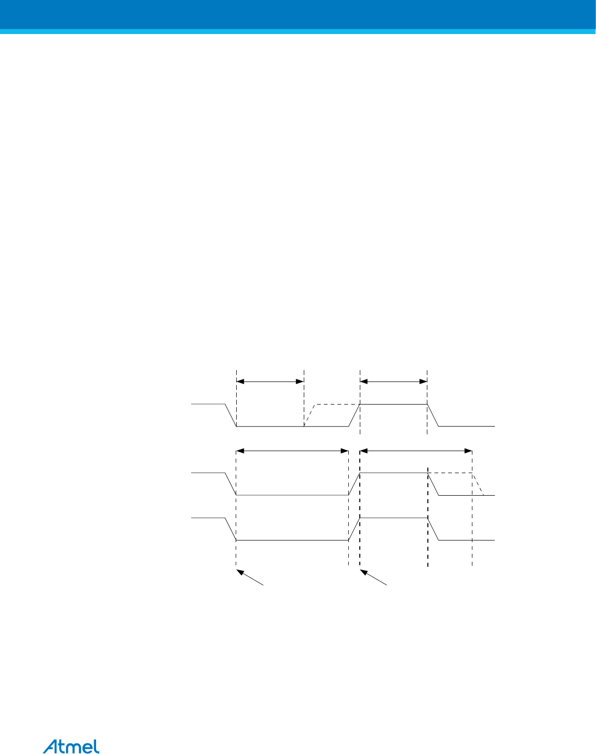
25.5. Multi-master Bus Systems, Arbitration and Synchronization
The TWI protocol allows bus systems with several masters. Special concerns have been taken in order to
ensure that transmissions will proceed as normal, even if two or more masters initiate a transmission at
the same time. Two problems arise in multi-master systems:
•An algorithm must be implemented allowing only one of the masters to complete the transmission.
All other masters should cease transmission when they discover that they have lost the selection
process. This selection process is called arbitration. When a contending master discovers that it
has lost the arbitration process, it should immediately switch to Slave mode to check whether it is
being addressed by the winning master. The fact that multiple masters have started transmission at
the same time should not be detectable to the slaves, i.e. the data being transferred on the bus
must not be corrupted.
•Different masters may use different SCL frequencies. A scheme must be devised to synchronize
the serial clocks from all masters, in order to let the transmission proceed in a lockstep fashion.
This will facilitate the arbitration process.
The wired-ANDing of the bus lines is used to solve both these problems. The serial clocks from all
masters will be wired-ANDed, yielding a combined clock with a high period equal to the one from the
Master with the shortest high period. The low period of the combined clock is equal to the low period of
the Master with the longest low period. Note that all masters listen to the SCL line, effectively starting to
count their SCL high and low time-out periods when the combined SCL line goes high or low,
respectively.
Figure 25-8 SCL Synchronization Between Multiple Masters
T Alow T Ahigh
SCL from
Master A
SCL from
Master B
SCL Bus
Line
TBlow TBhigh
Masters Star t
Counting Lo w P er iod
Masters Star t
Counting High P er iod
Arbitration is carried out by all masters continuously monitoring the SDA line after outputting data. If the
value read from the SDA line does not match the value the Master had output, it has lost the arbitration.
Note that a Master can only lose arbitration when it outputs a high SDA value while another Master
outputs a low value. The losing Master should immediately go to Slave mode, checking if it is being
addressed by the winning Master. The SDA line should be left high, but losing masters are allowed to
generate a clock signal until the end of the current data or address packet. Arbitration will continue until
only one Master remains, and this may take many bits. If several masters are trying to address the same
Slave, arbitration will continue into the data packet.
Atmel ATmega8A [DATASHEET]
Atmel-8159F-8-bit AVR Microcontroller_Datasheet_Complete-09/2015
217
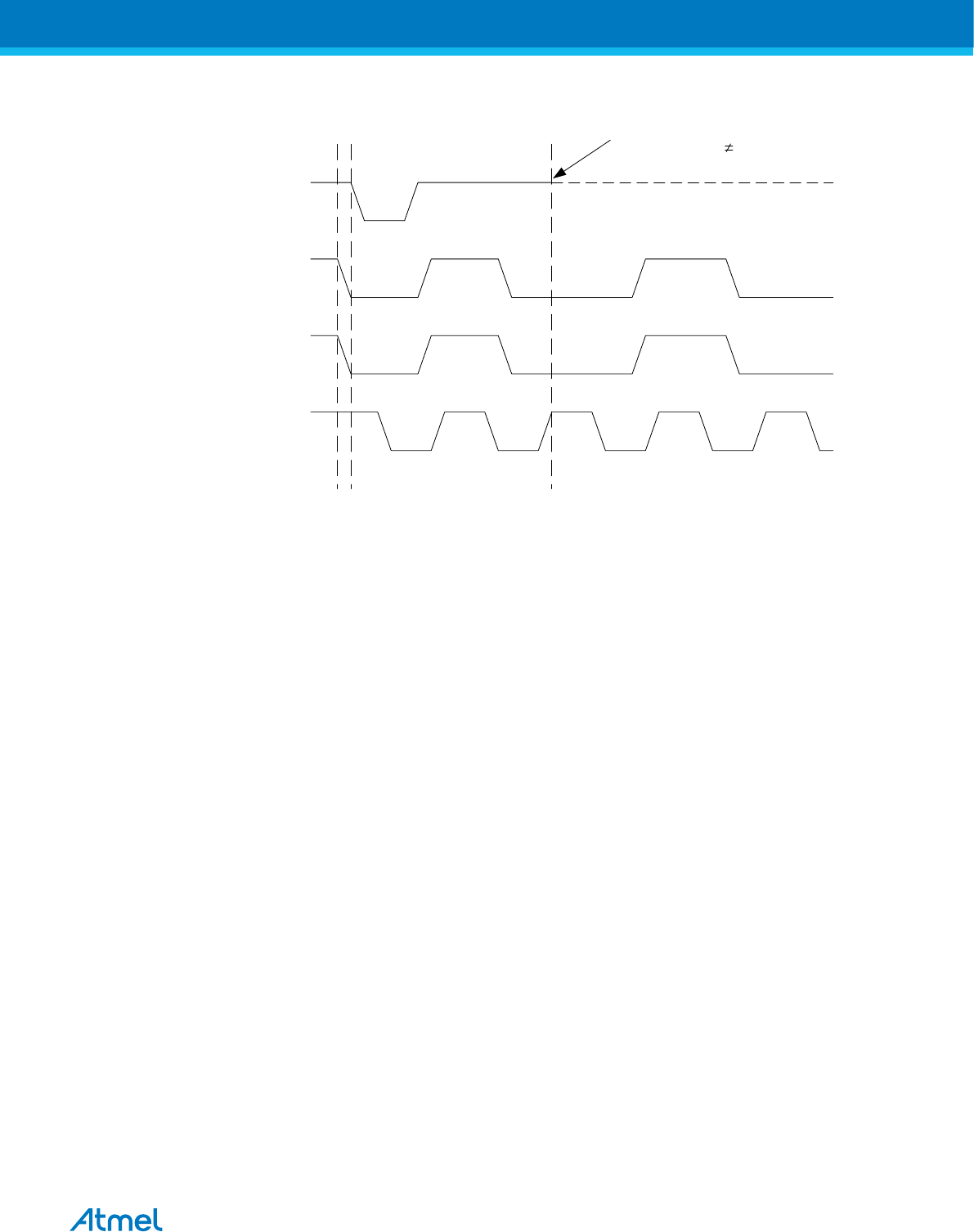
Figure 25-9 Arbitration Between Two Masters
SD A from
Master A
SD A from
Master B
SD A Line
Synchroniz ed
SCL Line
START Master A Loses
Arbitration, SD AA SD A
Note that arbitration is not allowed between:
•A REPEATED START condition and a data bit.
•A STOP condition and a data bit.
•A REPEATED START and a STOP condition.
It is the user software’s responsibility to ensure that these illegal arbitration conditions never occur. This
implies that in multi-master systems, all data transfers must use the same composition of SLA+R/W and
data packets. In other words: All transmissions must contain the same number of data packets, otherwise
the result of the arbitration is undefined.
25.6. Using the TWI
The AVR TWI is byte-oriented and interrupt based. Interrupts are issued after all bus events, like
reception of a byte or transmission of a START condition. Because the TWI is interrupt-based, the
application software is free to carry on other operations during a TWI byte transfer. Note that the TWI
Interrupt Enable (TWIE) bit in TWCR together with the Global Interrupt Enable bit in SREG allow the
application to decide whether or not assertion of the TWINT Flag should generate an interrupt request. If
the TWIE bit is cleared, the application must poll the TWINT Flag in order to detect actions on the TWI
bus.
When the TWINT Flag is asserted, the TWI has finished an operation and awaits application response. In
this case, the TWI Status Register (TWSR) contains a value indicating the current state of the TWI bus.
The application software can then decide how the TWI should behave in the next TWI bus cycle by
manipulating the TWCR and TWDR Registers.
The following figure is a simple example of how the application can interface to the TWI hardware. In this
example, a Master wishes to transmit a single data byte to a Slave. This description is quite abstract, a
more detailed explanation follows later in this section. A simple code example implementing the desired
behavior is also presented.
Atmel ATmega8A [DATASHEET]
Atmel-8159F-8-bit AVR Microcontroller_Datasheet_Complete-09/2015
218
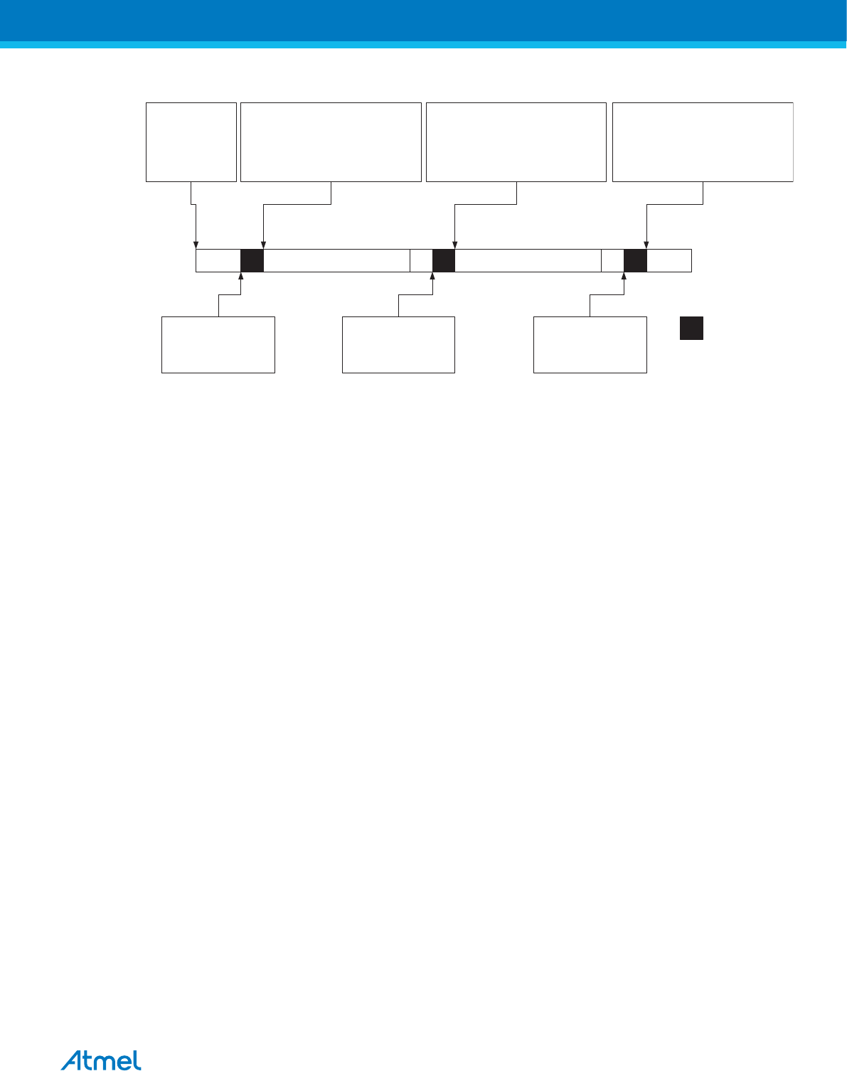
Figure 25-10 Interfacing the Application to the TWI in a Typical Transmission
START SLA+W A Data A STOP
1. Application
writes to TWCR to
initiate
transmission of
START
2.TWINT set.
Status code indicates
START condition sent
4.TWINT set.
Status code indicates
SLA+W sent, ACK
received
6.TWINT set.
Status code indicates
data sent, ACK received
3. Check TWSR to see if START was
sent. Application loads SLA+W into
TWDR, and loads appropriate control
signals into TWCR, making sure that
TWINT is written to one,
and TWSTA is written to zero.
5. CheckTWSR to see if SLA+W was
sent and ACK received.
Application loads data into TWDR, and
loads appropriate control signals into
TWCR, making sure that TWINT is
written to one
7. CheckTWSR to see if data was sent
and ACK received.
Application loads appropriate control
signals to send STOP into TWCR,
making sure that TWINT is written to one
TWI bus
Indicates
TWINT set
Application
Action
TWI
Hardware
Action
1. The first step in a TWI transmission is to transmit a START condition. This is done by writing a
specific value into TWCR, instructing the TWI hardware to transmit a START condition. Which value
to write is described later on. However, it is important that the TWINT bit is set in the value written.
Writing a one to TWINT clears the flag. The TWI will not start any operation as long as the TWINT
bit in TWCR is set. Immediately after the application has cleared TWINT, the TWI will initiate
transmission of the START condition.
2. When the START condition has been transmitted, the TWINT Flag in TWCR is set, and TWSR is
updated with a status code indicating that the START condition has successfully been sent.
3. The application software should now examine the value of TWSR, to make sure that the START
condition was successfully transmitted. If TWSR indicates otherwise, the application software might
take some special action, like calling an error routine. Assuming that the status code is as
expected, the application must load SLA+W into TWDR. Remember that TWDR is used both for
address and data. After TWDR has been loaded with the desired SLA+W, a specific value must be
written to TWCR, instructing the TWI hardware to transmit the SLA+W present in TWDR. Which
value to write is described later on. However, it is important that the TWINT bit is set in the value
written. Writing a one to TWINT clears the flag. The TWI will not start any operation as long as the
TWINT bit in TWCR is set. Immediately after the application has cleared TWINT, the TWI will initiate
transmission of the address packet.
4. When the address packet has been transmitted, the TWINT Flag in TWCR is set, and TWSR is
updated with a status code indicating that the address packet has successfully been sent. The
status code will also reflect whether a Slave acknowledged the packet or not.
5. The application software should now examine the value of TWSR, to make sure that the address
packet was successfully transmitted, and that the value of the ACK bit was as expected. If TWSR
indicates otherwise, the application software might take some special action, like calling an error
routine. Assuming that the status code is as expected, the application must load a data packet into
TWDR. Subsequently, a specific value must be written to TWCR, instructing the TWI hardware to
transmit the data packet present in TWDR. Which value to write is described later on. However, it is
important that the TWINT bit is set in the value written. Writing a one to TWINT clears the flag. The
TWI will not start any operation as long as the TWINT bit in TWCR is set. Immediately after the
application has cleared TWINT, the TWI will initiate transmission of the data packet.
6. When the data packet has been transmitted, the TWINT Flag in TWCR is set, and TWSR is
updated with a status code indicating that the data packet has successfully been sent. The status
code will also reflect whether a Slave acknowledged the packet or not.
Atmel ATmega8A [DATASHEET]
Atmel-8159F-8-bit AVR Microcontroller_Datasheet_Complete-09/2015
219

7. The application software should now examine the value of TWSR, to make sure that the data
packet was successfully transmitted, and that the value of the ACK bit was as expected. If TWSR
indicates otherwise, the application software might take some special action, like calling an error
routine. Assuming that the status code is as expected, the application must write a specific value to
TWCR, instructing the TWI hardware to transmit a STOP condition. Which value to write is
described later on. However, it is important that the TWINT bit is set in the value written. Writing a
one to TWINT clears the flag. The TWI will not start any operation as long as the TWINT bit in
TWCR is set. Immediately after the application has cleared TWINT, the TWI will initiate
transmission of the STOP condition. Note that TWINT is NOT set after a STOP condition has been
sent.
Even though this example is simple, it shows the principles involved in all TWI transmissions. These can
be summarized as follows:
•When the TWI has finished an operation and expects application response, the TWINT Flag is set.
The SCL line is pulled low until TWINT is cleared.
•When the TWINT Flag is set, the user must update all TWI Registers with the value relevant for the
next TWI bus cycle. As an example, TWDR must be loaded with the value to be transmitted in the
next bus cycle.
•After all TWI Register updates and other pending application software tasks have been completed,
TWCR is written. When writing TWCR, the TWINT bit should be set. Writing a one to TWINT clears
the flag. The TWI will then commence executing whatever operation was specified by the TWCR
setting.
The following table lists assembly and C implementation examples. Note that the code below assumes
that several definitions have been made, e.g. by using include-files.
Table 25-2 Assembly and C Code Example
Assembly Code Example C Example Comments
1ldi r16, (1<<TWINT)|(1<<TWSTA)|
(1<<TWEN)
out TWCR, r16
TWCR = (1<<TWINT)|
(1<<TWSTA)|(1<<TWEN) Send START condition
2
wait1:
in r16,TWCR
sbrs r16,TWINT
rjmp wait1
while (!(TWCR &
(1<<TWINT)));
Wait for TWINT Flag set. This indicates
that the START condition has been
transmitted.
3
in r16,TWSR
andi r16, 0xF8
cpi r16, START
brne ERROR
if ((TWSR & 0xF8) !=
START)
ERROR();
Check value of TWI Status Register.
Mask prescaler bits. If status different
from START go to ERROR.
ldi r16, SLA_W
out TWDR, r16
ldi r16, (1<<TWINT) | (1<<TWEN)
out TWCR, r16
TWDR = SLA_W;
TWCR = (1<<TWINT) |
(1<<TWEN);
Load SLA_W into TWDR Register. Clear
TWINT bit in TWCR to start transmission
of address.
4
wait2:
in r16,TWCR
sbrs r16,TWINT
rjmp wait2
while (!(TWCR &
(1<<TWINT)));
Wait for TWINT Flag set. This indicates
that the SLA+W has been transmitted,
and ACK/NACK has been received.
5
in r16,TWSR
andi r16, 0xF8
cpi r16, MT_SLA_ACK
brne ERROR
if ((TWSR & 0xF8) !=
MT_SLA_ACK)
ERROR();
Check value of TWI Status Register.
Mask prescaler bits. If status different
from MT_SLA_ACK go to ERROR.
ldi r16, DATA
out TWDR, r16
ldi r16, (1<<TWINT) | (1<<TWEN)
out TWCR, r16
TWDR = DATA;
TWCR = (1<<TWINT) |
(1<<TWEN);
Load DATA into TWDR Register. Clear
TWINT bit in TWCR to start transmission
of data.
Atmel ATmega8A [DATASHEET]
Atmel-8159F-8-bit AVR Microcontroller_Datasheet_Complete-09/2015
220
Assembly Code Example C Example Comments
6
wait3:
in r16,TWCR
sbrs r16,TWINT
rjmp wait3
while (!(TWCR &
(1<<TWINT)));
Wait for TWINT Flag set. This indicates
that the DATA has been transmitted, and
ACK/NACK has been received.
7
in r16,TWSR
andi r16, 0xF8
cpi r16, MT_DATA_ACK
brne ERROR
if ((TWSR & 0xF8) !=
MT_DATA_ACK)
ERROR();
Check value of TWI Status Register.
Mask prescaler bits. If status different
from MT_DATA_ACK go to ERROR.
ldi r16, (1<<TWINT)|(1<<TWEN)|
(1<<TWSTO)
out TWCR, r16
TWCR = (1<<TWINT)|
(1<<TWEN)|(1<<TWSTO); Transmit STOP condition.
25.6.1. Transmission Modes
The TWI can operate in one of four major modes:
•Master Transmitter (MT)
•Master Receiver (MR)
•Slave Transmitter (ST)
•Slave Receiver (SR)
Several of these modes can be used in the same application. As an example, the TWI can use MT mode
to write data into a TWI EEPROM, MR mode to read the data back from the EEPROM. If other masters
are present in the system, some of these might transmit data to the TWI, and then SR mode would be
used. It is the application software that decides which modes are legal.
The following sections describe each of these modes. Possible status codes are described along with
figures detailing data transmission in each of the modes. These figures use the following abbreviations:
S START condition
Rs REPEATED START condition
R Read bit (high level at SDA)
W Write bit (low level at SDA)
A Acknowledge bit (low level at SDA)
A Not acknowledge bit (high level at SDA)
Data 8-bit data byte
P STOP condition
SLA Slave Address
Circles are used to indicate that the TWINT Flag is set. The numbers in the circles show the status code
held in TWSR, with the prescaler bits masked to zero. At these points, actions must be taken by the
application to continue or complete the TWI transfer. The TWI transfer is suspended until the TWINT Flag
is cleared by software.
When the TWINT Flag is set, the status code in TWSR is used to determine the appropriate software
action. For each status code, the required software action and details of the following serial transfer are
given below in the Status Code table for each mode. Note that the prescaler bits are masked to zero in
these tables.
Atmel ATmega8A [DATASHEET]
Atmel-8159F-8-bit AVR Microcontroller_Datasheet_Complete-09/2015
221
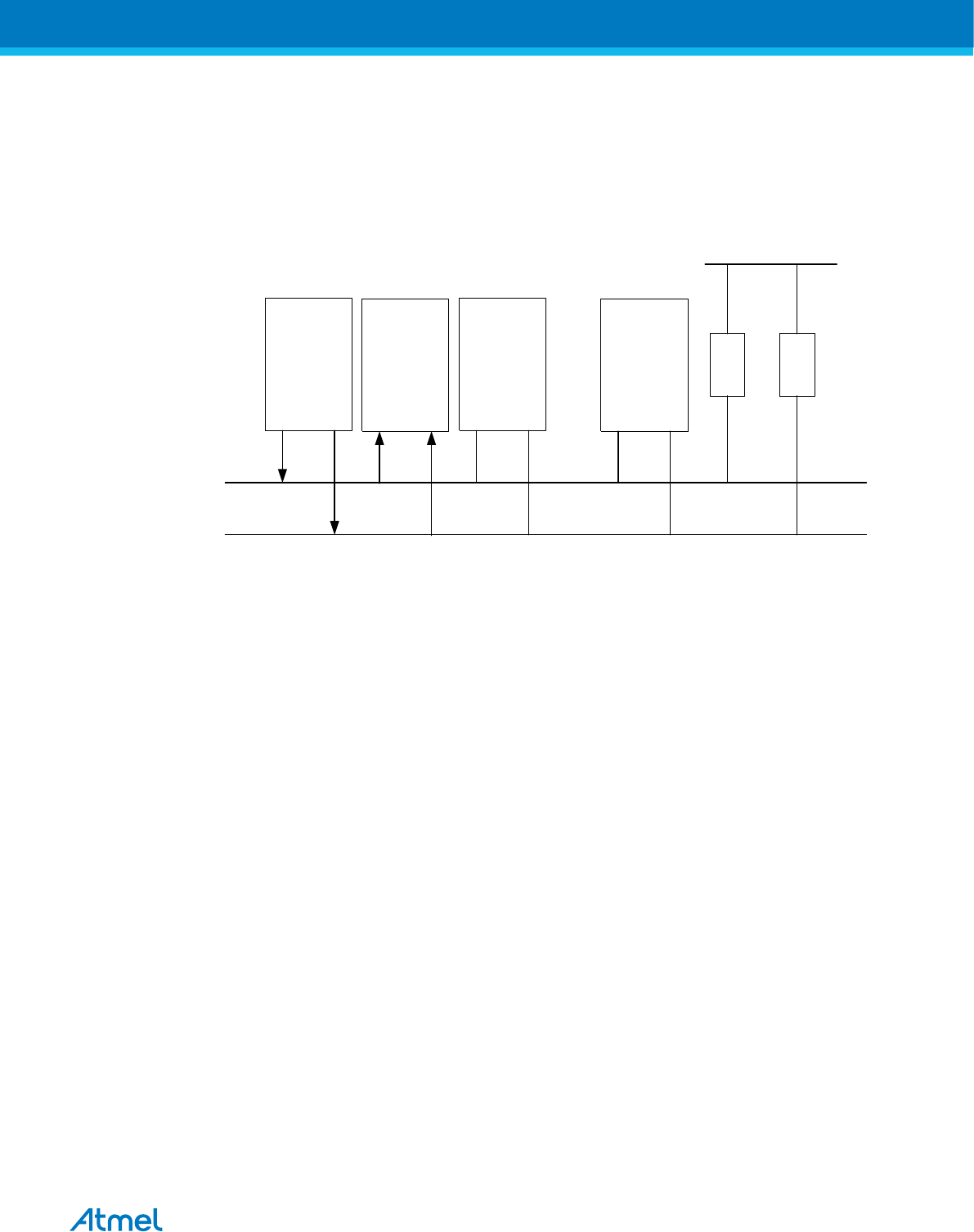
25.6.2. Master Transmitter Mode
In the Master Transmitter (MT) mode, a number of data bytes are transmitted to a Slave Receiver, see
figure below. In order to enter a Master mode, a START condition must be transmitted. The format of the
following address packet determines whether MT or Master Receiver (MR) mode is to be entered: If SLA
+W is transmitted, MT mode is entered, if SLA+R is transmitted, MR mode is entered. All the status codes
mentioned in this section assume that the prescaler bits are zero or are masked to zero.
Figure 25-11 Data Transfer in Master Transmitter Mode
Device 1
MASTER
TRANSMITTER
Device 2
SLA VE
RECEIVER
Device 3 Device n
SD A
SCL
........ R1 R2
VCC
A START condition is sent by writing a value to the TWI Control Register (TWCR) of the type
TWCR=1x10x10x:
•The TWI Enable bit (TWCR.TWEN) must be written to '1' to enable the 2-wire Serial Interface
•The TWI Start Condition bit (TWCR.TWSTA) must be written to '1' to transmit a START condition
•The TWI Interrupt Flag (TWCR.TWINT) must be written to '1' to clear the flag.
The TWI will then test the 2-wire Serial Bus and generate a START condition as soon as the bus
becomes free. After a START condition has been transmitted, the TWINT Flag is set by hardware, and
the status code in TWSR will be 0x08 (see Status Code table below). In order to enter MT mode, SLA+W
must be transmitted. This is done by writing SLA+W to the TWI Data Register (TWDR). Thereafter, the
TWCR.TWINT Flag should be cleared (by writing a '1' to it) to continue the transfer. This is accomplished
by writing a value to TWRC of the type TWCR=1x00x10x.
When SLA+W have been transmitted and an acknowledgment bit has been received, TWINT is set again
and a number of status codes in TWSR are possible. Possible status codes in Master mode are 0x18,
0x20, or 0x38. The appropriate action to be taken for each of these status codes is detailed in the Status
Code table below.
When SLA+W has been successfully transmitted, a data packet should be transmitted. This is done by
writing the data byte to TWDR. TWDR must only be written when TWINT is high. If not, the access will be
discarded, and the Write Collision bit (TWWC) will be set in the TWCR Register. After updating TWDR,
the TWINT bit should be cleared (by writing '1' to it) to continue the transfer. This is accomplished by
writing again a value to TWCR of the type TWCR=1x00x10x.
This scheme is repeated until the last byte has been sent and the transfer is ended, either by generating
a STOP condition or a by a repeated START condition. A repeated START condition is accomplished by
writing a regular START value TWCR=1x10x10x. A STOP condition is generated by writing a value of the
type TWCR=1x01x10x.
After a repeated START condition (status code 0x10), the 2-wire Serial Interface can access the same
Slave again, or a new Slave without transmitting a STOP condition. Repeated START enables the Master
Atmel ATmega8A [DATASHEET]
Atmel-8159F-8-bit AVR Microcontroller_Datasheet_Complete-09/2015
222
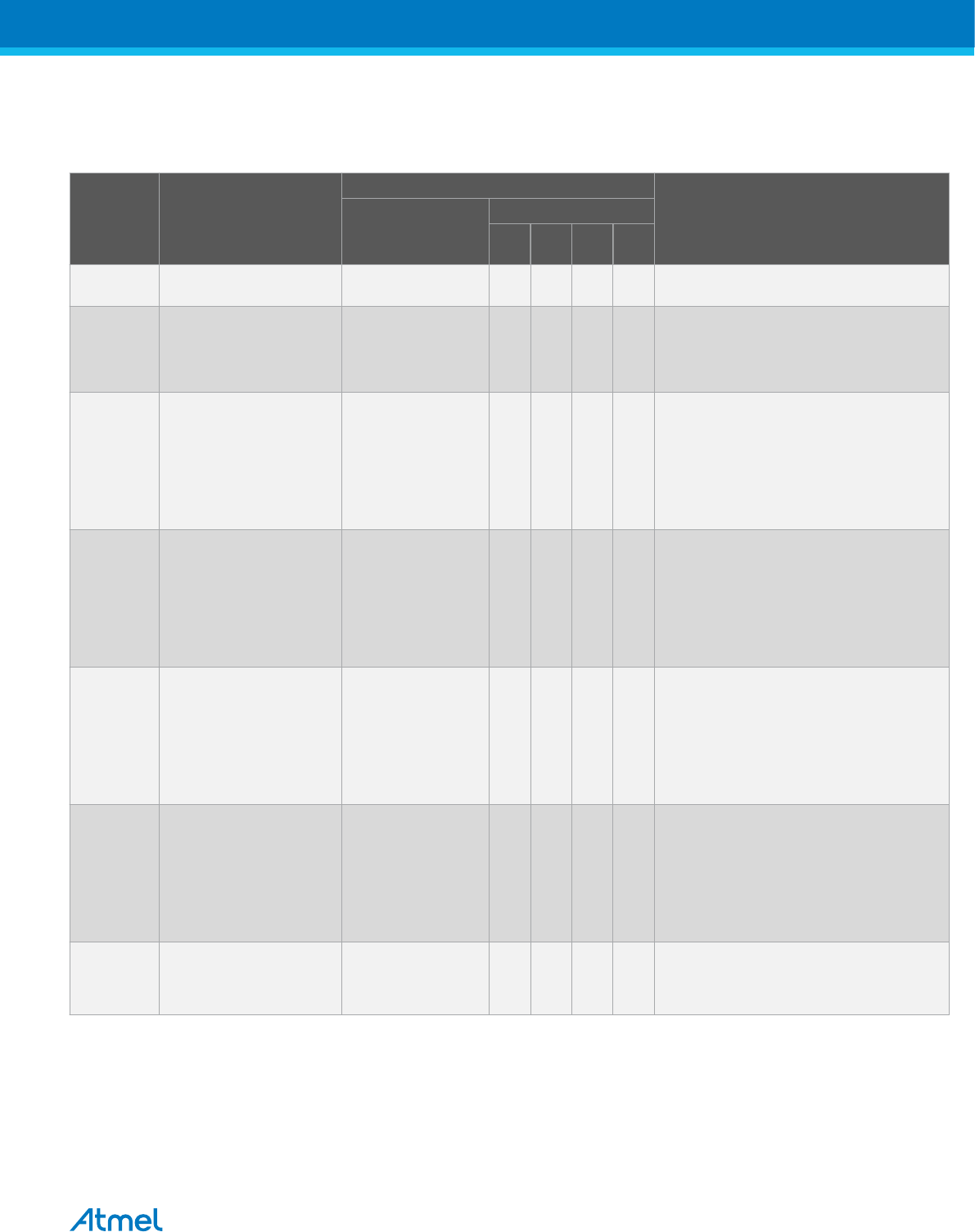
to switch between Slaves, Master Transmitter mode and Master Receiver mode without losing control of
the bus.
Table 25-3 Status Codes for Master Transmitter Mode
Status Code
(TWSR)
Prescaler Bits
are 0
Status of the 2-wire Serial Bus
and 2-wire Serial Interface
Hardware
Application Software Response Next Action Taken by TWI Hardware
To/from TWDR To TWCR
STA STO TWIN
T
TWE
A
0x08 A START condition has been
transmitted
Load SLA+W 0 0 1 X SLA+W will be transmitted;
ACK or NOT ACK will be received
0x10 A repeated START condition has
been transmitted
Load SLA+W or
Load SLA+R
0
0
0
0
1
1
X
X
SLA+W will be transmitted;
ACK or NOT ACK will be received
SLA+R will be transmitted;
Logic will switch to Master Receiver mode
0x18 SLA+W has been transmitted;
ACK has been received
Load data byte or
No TWDR action or
No TWDR action or
No TWDR action
0
1
0
1
0
0
1
1
1
1
1
1
X
X
X
X
Data byte will be transmitted and ACK or NOT ACK will
be received
Repeated START will be transmitted
STOP condition will be transmitted and
TWSTO Flag will be reset
STOP condition followed by a START condition will be
transmitted and TWSTO Flag will be reset
0x20 SLA+W has been transmitted;
NOT ACK has been received
Load data byte or
No TWDR action or
No TWDR action or
No TWDR action
0
1
0
1
0
0
1
1
1
1
1
1
X
X
X
X
Data byte will be transmitted and ACK or NOT ACK will
be received
Repeated START will be transmitted
STOP condition will be transmitted and
TWSTO Flag will be reset
STOP condition followed by a START condition will be
transmitted and TWSTO Flag will be reset
0x28 Data byte has been transmitted;
ACK has been received
Load data byte or
No TWDR action or
No TWDR action or
No TWDR action
0
1
0
1
0
0
1
1
1
1
1
1
X
X
X
X
Data byte will be transmitted and ACK or NOT ACK will
be received
Repeated START will be transmitted
STOP condition will be transmitted and
TWSTO Flag will be reset
STOP condition followed by a START condition will be
transmitted and TWSTO Flag will be reset
0x30 Data byte has been transmitted;
NOT ACK has been received
Load data byte or
No TWDR action or
No TWDR action or
No TWDR action
0
1
0
1
0
0
1
1
1
1
1
1
X
X
X
X
Data byte will be transmitted and ACK or NOT ACK will
be received
Repeated START will be transmitted
STOP condition will be transmitted and
TWSTO Flag will be reset
STOP condition followed by a START condition will be
transmitted and TWSTO Flag will be reset
0x38 Arbitration lost in SLA+W or data
bytes
No TWDR action or
No TWDR action
0
1
0
0
1
1
X
X
2-wire Serial Bus will be released and not addressed
Slave mode entered
A START condition will be transmitted when the bus
becomes free
Atmel ATmega8A [DATASHEET]
Atmel-8159F-8-bit AVR Microcontroller_Datasheet_Complete-09/2015
223
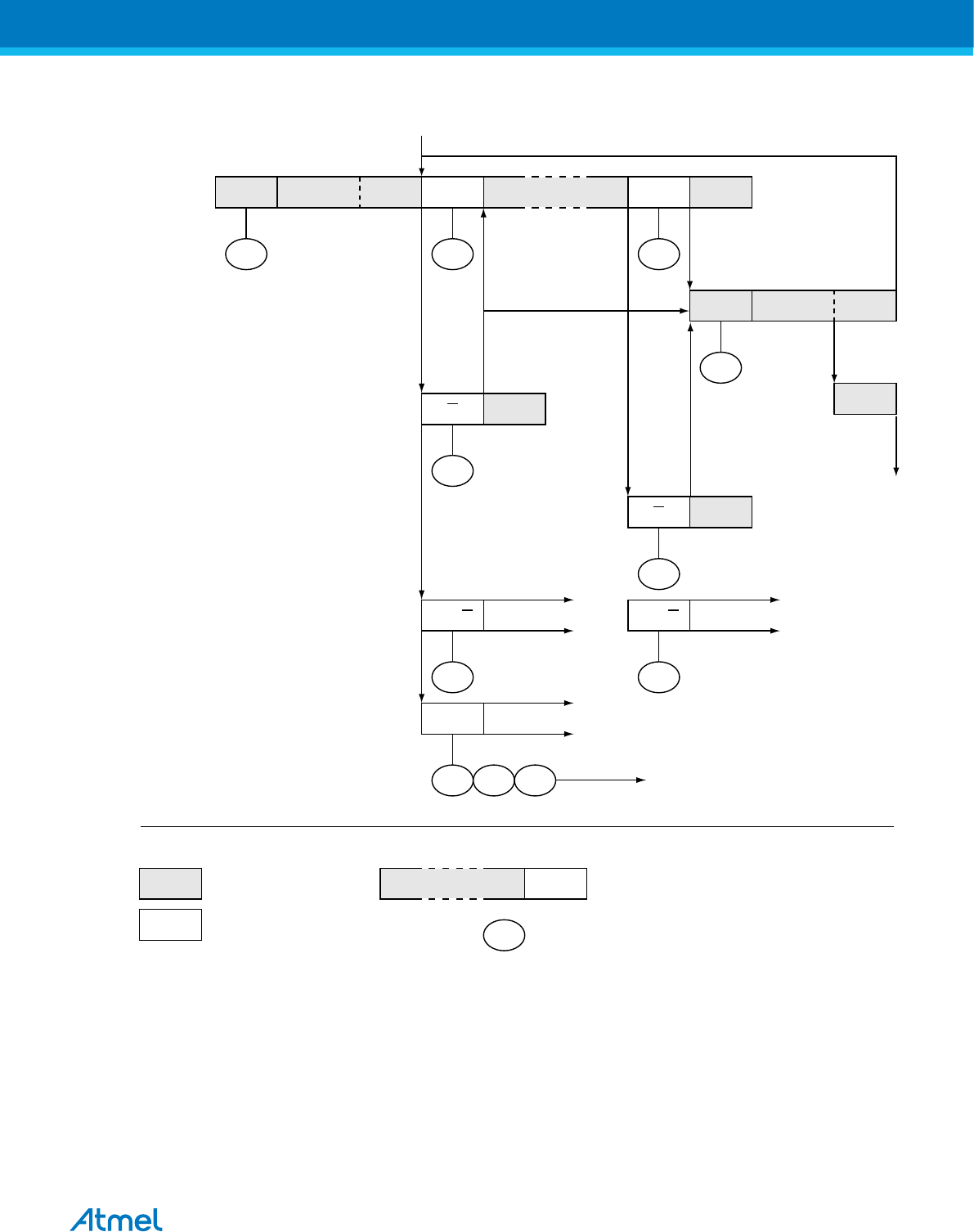
Figure 25-12 Formats and States in the Master Transmitter Mode
S SLA W A DAT A A P
$08 $18 $28
R SLA W
$10
A P
$20
P
$30
A or A
$38
A
Other master
contin ues
A or A
$38
Other master
contin ues
R
A
$68
Other master
contin ues
$78 $B0
To corresponding
states in sla v e mode
MT
MR
Successfull
transmission
to a sla v e
receiv er
Next transfer
star ted with a
repeated star t
condition
Not acknowledge
received after the
slave address
Not acknowledge
receiv ed after a data
byte
Arbitration lost in sla v e
address or data b yte
Arbitration lost and
addressed as sla v e
DAT A A
n
From master to sla v e
From sla v e to master
Any number of data b ytes
and their associated ac kno wledge bits
This number (contained in TWSR) corresponds
to a defined state of the 2-Wire Ser ial Bus. The
prescaler bits are z ero or mask ed to z ero
S
25.6.3. Master Receiver Mode
In the Master Receiver (MR) mode, a number of data bytes are received from a Slave Transmitter (see
next figure). In order to enter a Master mode, a START condition must be transmitted. The format of the
following address packet determines whether Master Transmitter (MT) or MR mode is to be entered. If
SLA+W is transmitted, MT mode is entered, if SLA+R is transmitted, MR mode is entered. All the status
codes mentioned in this section assume that the prescaler bits are zero or are masked to zero.
Atmel ATmega8A [DATASHEET]
Atmel-8159F-8-bit AVR Microcontroller_Datasheet_Complete-09/2015
224
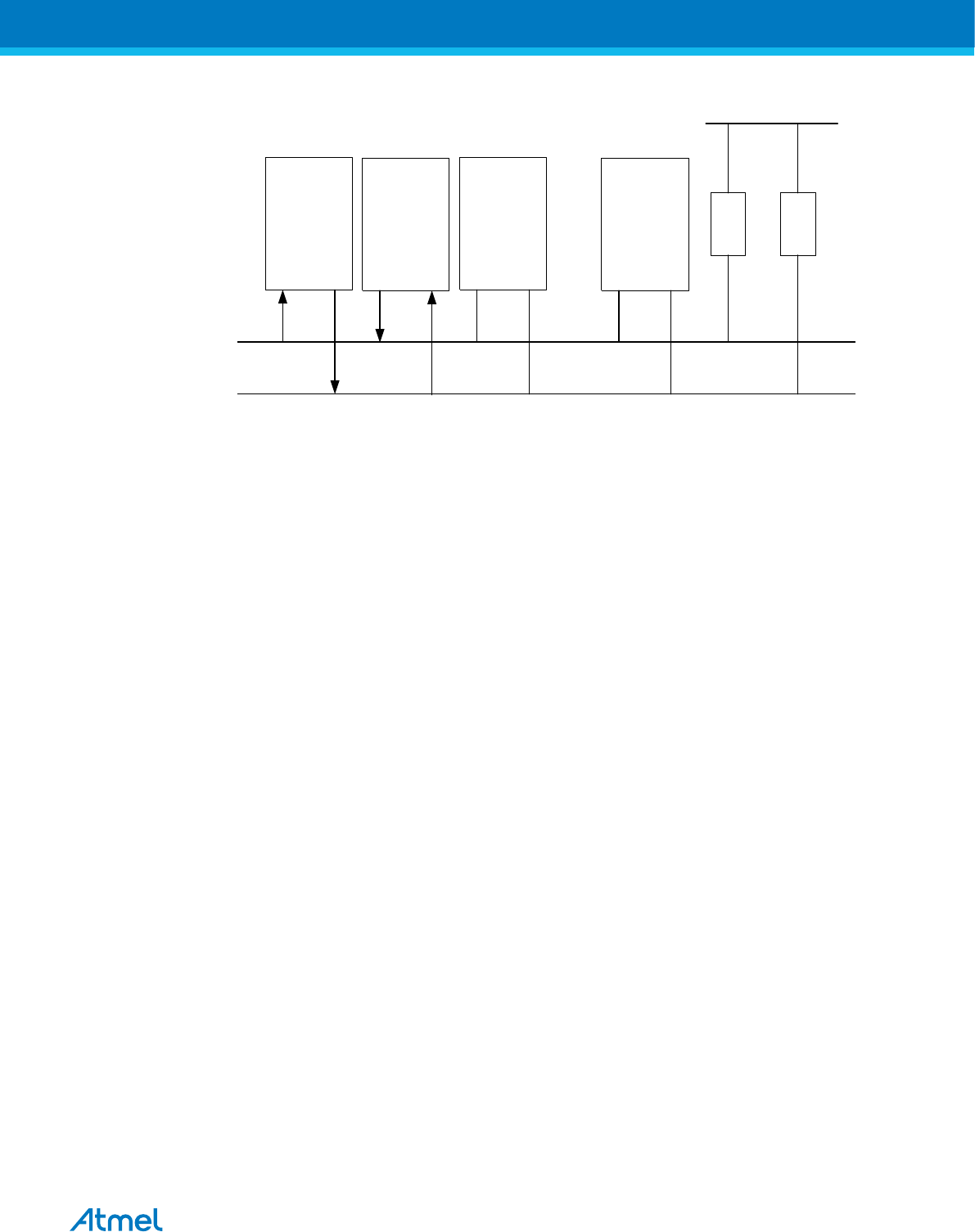
Figure 25-13 Data Transfer in Master Receiver Mode
Device 1
MASTER
RECEIVER
Device 2
SLA VE
TRANSMITTER
Device 3 Device n
SD A
SCL
........ R1 R2
VCC
A START condition is sent by writing to the TWI Control register (TWCR) a value of the type
TWCR=1x10x10x:
•TWCR.TWEN must be written to '1' to enable the 2-wire Serial Interface
•TWCR.TWSTA must be written to '1' to transmit a START condition
•TWCR.TWINT must be cleared by writing a '1' to it.
The TWI will then test the 2-wire Serial Bus and generate a START condition as soon as the bus
becomes free. After a START condition has been transmitted, the TWINT Flag is set by hardware, and
the status code in TWSR will be 0x08 (see Status Code table below). In order to enter MR mode, SLA+R
must be transmitted. This is done by writing SLA+R to TWDR. Thereafter, the TWINT flag should be
cleared (by writing '1' to it) to continue the transfer. This is accomplished by writing the a value to TWCR
of the type TWCE=1x00x10x.
When SLA+R have been transmitted and an acknowledgment bit has been received, TWINT is set again
and a number of status codes in TWSR are possible. Possible status codes in Master mode are 0x38,
0x40, or 0x48. The appropriate action to be taken for each of these status codes is detailed in the table
below. Received data can be read from the TWDR Register when the TWINT Flag is set high by
hardware. This scheme is repeated until the last byte has been received. After the last byte has been
received, the MR should inform the ST by sending a NACK after the last received data byte. The transfer
is ended by generating a STOP condition or a repeated START condition. A repeated START condition is
sent by writing to the TWI Control register (TWCR) a value of the type TWCR=1x10x10x again. A STOP
condition is generated by writing TWCR=1xx01x10x:
After a repeated START condition (status code 0x10) the 2-wire Serial Interface can access the same
Slave again, or a new Slave without transmitting a STOP condition. Repeated START enables the Master
to switch between Slaves, Master Transmitter mode and Master Receiver mode without losing control
over the bus.
Atmel ATmega8A [DATASHEET]
Atmel-8159F-8-bit AVR Microcontroller_Datasheet_Complete-09/2015
225

Table 25-4 Status codes for Master Receiver Mode
Status Code
(TWSR)
Prescaler Bits
are 0
Status of the 2-wire Serial Bus
and 2-wire Serial Interface
Hardware
Application Software Response Next Action Taken by TWI Hardware
To/from TWD To TWCR
STA STO TWIN
T
TWE
A
0x08 A START condition has been
transmitted
Load SLA+R 0 0 1 X SLA+R will be transmitted
ACK or NOT ACK will be received
0x10 A repeated START condition has
been transmitted
Load SLA+R or
Load SLA+W
0
0
0
0
1
1
X
X
SLA+R will be transmitted
ACK or NOT ACK will be received
SLA+W will be transmitted
Logic will switch to Master Transmitter mode
0x38 Arbitration lost in SLA+R or NOT
ACK bit
No TWDR action or
No TWDR action
0
1
0
0
1
1
X
X
2-wire Serial Bus will be released and not addressed
Slave mode will be entered
A START condition will be transmitted when the bus
becomes free
0x40 SLA+R has been transmitted;
ACK has been received
No TWDR action or
No TWDR action
0
0
0
0
1
1
0
1
Data byte will be received and NOT ACK will be
returned
Data byte will be received and ACK will be returned
0x48 SLA+R has been transmitted;
NOT ACK has been received
No TWDR action or
No TWDR action or
No TWDR action
1
0
1
0
1
1
1
1
1
X
X
X
Repeated START will be transmitted
STOP condition will be transmitted and TWSTO Flag
will be reset
STOP condition followed by a START condition will be
transmitted and TWSTO Flag will be reset
0x50 Data byte has been received;
ACK has been returned
Read data byte or
Read data byte
0
0
0
0
1
1
0
1
Data byte will be received and NOT ACK will be
returned
Data byte will be received and ACK will be returned
0x58 Data byte has been received;
NOT ACK has been returned
Read data byte or
Read data byte or
Read data byte
1
0
1
0
1
1
1
1
1
X
X
X
Repeated START will be transmitted
STOP condition will be transmitted and TWSTO Flag
will be reset
STOP condition followed by a START condition will be
transmitted and TWSTO Flag will be reset
Atmel ATmega8A [DATASHEET]
Atmel-8159F-8-bit AVR Microcontroller_Datasheet_Complete-09/2015
226
Figure 25-14 Formats and States in the Master Receiver Mode
S SLA R A DAT A A
$08 $40 $50
SLA R
$10
A P
$48
A or A
$38
Other master
contin ues
$38
Other master
contin ues
W
A
$68
Other master
contin ues
$78 $B0
To corresponding
states in sla v e mode
MR
MT
Successfull
reception
from a sla v e
receiv er
Next transf er
star ted with a
repeated star t
condition
Not ac kno wledge
received after the
slave address
Arbitration lost in sla v e
address or data b yte
Arbitration lost and
addressed as sla v e
DAT A A
n
From master to sla v e
From slave to master
Any number of data b ytes
and their associated ac kno wledge bits
This number (contained in TWSR) corresponds
to a defined state of the 2-Wire Ser ial Bus. The
prescaler bits are z ero or mask ed to z ero
PDATA A
$58
A
RS
25.6.4. Slave Receiver Mode
In the Slave Receiver (SR) mode, a number of data bytes are received from a Master Transmitter (see
figure below). All the status codes mentioned in this section assume that the prescaler bits are zero or are
masked to zero.
Atmel ATmega8A [DATASHEET]
Atmel-8159F-8-bit AVR Microcontroller_Datasheet_Complete-09/2015
227

Figure 25-15 Data transfer in Slave Receiver mode
Device 3 Device n
SD A
SCL
........ R1 R2
VCC
Device 2
MASTER
TRANSMITTER
Device 1
SLA VE
RECEIVER
To initiate the SR mode, the TWI (Slave) Address Register (TWAR) and the TWI Control Register
(TWCR) must be initialized as follows:
The upper seven bits of TWAR are the address to which the 2-wire Serial Interface will respond when
addressed by a Master (TWAR.TWA[6:0]). If the LSB of TWAR is written to TWAR.TWGCI=1, the TWI will
respond to the general call address (0x00), otherwise it will ignore the general call address.
TWCR must hold a value of the type TWCR=0100010x - TWCR.TWEN must be written to '1' to enable
the TWI. TWCR.TWEA bit must be written to '1' to enable the acknowledgement of the device’s own slave
address or the general call address. TWCR.TWSTA and TWSTO must be written to zero.
When TWAR and TWCR have been initialized, the TWI waits until it is addressed by its own slave
address (or the general call address, if enabled) followed by the data direction bit. If the direction bit is '0'
(write), the TWI will operate in SR mode, otherwise ST mode is entered. After its own slave address and
the write bit have been received, the TWINT Flag is set and a valid status code can be read from TWSR.
The status code is used to determine the appropriate software action, as detailed in the table below. The
SR mode may also be entered if arbitration is lost while the TWI is in the Master mode (see states 0x68
and 0x78).
If the TWCR.TWEA bit is reset during a transfer, the TWI will return a "Not Acknowledge" ('1') to SDA
after the next received data byte. This can be used to indicate that the Slave is not able to receive any
more bytes. While TWEA is zero, the TWI does not acknowledge its own slave address. However, the 2-
wire Serial Bus is still monitored and address recognition may resume at any time by setting TWEA. This
implies that the TWEA bit may be used to temporarily isolate the TWI from the 2-wire Serial Bus.
In all sleep modes other than Idle mode, the clock system to the TWI is turned off. If the TWEA bit is set,
the interface can still acknowledge its own slave address or the general call address by using the 2-wire
Serial Bus clock as a clock source. The part will then wake up from sleep and the TWI will hold the SCL
clock low during the wake up and until the TWINT Flag is cleared (by writing '1' to it). Further data
reception will be carried out as normal, with the AVR clocks running as normal. Observe that if the AVR is
set up with a long start-up time, the SCL line may be held low for a long time, blocking other data
transmissions.
Note: The 2-wire Serial Interface Data Register (TWDR) does not reflect the last byte present on the bus
when waking up from these Sleep modes.
Atmel ATmega8A [DATASHEET]
Atmel-8159F-8-bit AVR Microcontroller_Datasheet_Complete-09/2015
228

Table 25-5 Status Codes for Slave Receiver Mode
Status
Code
(TWSR)
Prescaler
Bits are 0
Status of the 2-wire Serial
Bus and 2-wire Serial
Interface Hardware
Application Software Response Next Action Taken by TWI Hardware
To/from TWDR To TWCR
STA STO TWI
NT
TWE
A
0x60 Own SLA+W has been
received;
ACK has been returned
No TWDR action
or
No TWDR action
X
X
0
0
1
1
0
1
Data byte will be received and NOT ACK will be
returned
Data byte will be received and ACK will be returned
0x68 Arbitration lost in SLA+R/W
as Master; own SLA+W has
been
received; ACK has been
returned
No TWDR action
or
No TWDR action
X
X
0
0
1
1
0
1
Data byte will be received and NOT ACK will be
returned
Data byte will be received and ACK will be returned
0x70 General call address has
been
received; ACK has been
returned
No TWDR action
or
No TWDR action
X
X
0
0
1
1
0
1
Data byte will be received and NOT ACK will be
returned
Data byte will be received and ACK will be returned
0x78 Arbitration lost in SLA+R/W
as Master; General call
address has been received;
ACK has been returned
No TWDR action
or
No TWDR action
X
X
0
0
1
1
0
1
Data byte will be received and NOT ACK will be
returned
Data byte will be received and ACK will be returned
0x80 Previously addressed with
own SLA+W; data has been
received; ACK has been
returned
Read data byte or
Read data byte
X
X
0
0
1
1
0
1
Data byte will be received and NOT ACK will be
returned
Data byte will be received and ACK will be returned
0x88 Previously addressed with
own SLA+W; data has been
received; NOT ACK has been
returned
Read data byte or
Read data byte or
Read data byte or
Read data byte
0
0
1
1
0
0
0
0
1
1
1
1
0
1
0
1
Switched to the not addressed Slave mode;
no recognition of own SLA or GCA
Switched to the not addressed Slave mode;
own SLA will be recognized;
GCA will be recognized if TWGCE = “1”
Switched to the not addressed Slave mode;
no recognition of own SLA or GCA;
a START condition will be transmitted when the bus
becomes free
Switched to the not addressed Slave mode;
own SLA will be recognized;
GCA will be recognized if TWGCE = “1”; a START
condition will be transmitted when the bus becomes
free
0x90 Previously addressed with
general call; data has been
received; ACK has been
returned
Read data byte or
Read data byte
X
X
0
0
1
1
0
1
Data byte will be received and NOT ACK will be
returned
Data byte will be received and ACK will be returned
Atmel ATmega8A [DATASHEET]
Atmel-8159F-8-bit AVR Microcontroller_Datasheet_Complete-09/2015
229

Status
Code
(TWSR)
Prescaler
Bits are 0
Status of the 2-wire Serial
Bus and 2-wire Serial
Interface Hardware
Application Software Response Next Action Taken by TWI Hardware
To/from TWDR To TWCR
STA STO TWI
NT
TWE
A
0x98 Previously addressed with
general call; data has been
received; NOT ACK has been
returned
Read data byte or
Read data byte or
Read data byte or
Read data byte
0
0
1
1
0
0
0
0
1
1
1
1
0
1
0
1
Switched to the not addressed Slave mode;
no recognition of own SLA or GCA
Switched to the not addressed Slave mode;
own SLA will be recognized;
GCA will be recognized if TWGCE = “1”
Switched to the not addressed Slave mode;
no recognition of own SLA or GCA;
a START condition will be transmitted when the bus
becomes free
Switched to the not addressed Slave mode;
own SLA will be recognized;
GCA will be recognized if TWGCE = “1”; a START
condition will be transmitted when the bus becomes
free
0xA0 A STOP condition or repeated
START condition has been
received while still addressed
as Slave
No action 0
0
1
1
0
0
0
0
1
1
1
1
0
1
0
1
Switched to the not addressed Slave mode;
no recognition of own SLA or GCA
Switched to the not addressed Slave mode;
own SLA will be recognized;
GCA will be recognized if TWGCE = “1”
Switched to the not addressed Slave mode;
no recognition of own SLA or GCA;
a START condition will be transmitted when the bus
becomes free
Switched to the not addressed Slave mode;
own SLA will be recognized;
GCA will be recognized if TWGCE = “1”; a START
condition will be transmitted when the bus becomes
free
Atmel ATmega8A [DATASHEET]
Atmel-8159F-8-bit AVR Microcontroller_Datasheet_Complete-09/2015
230
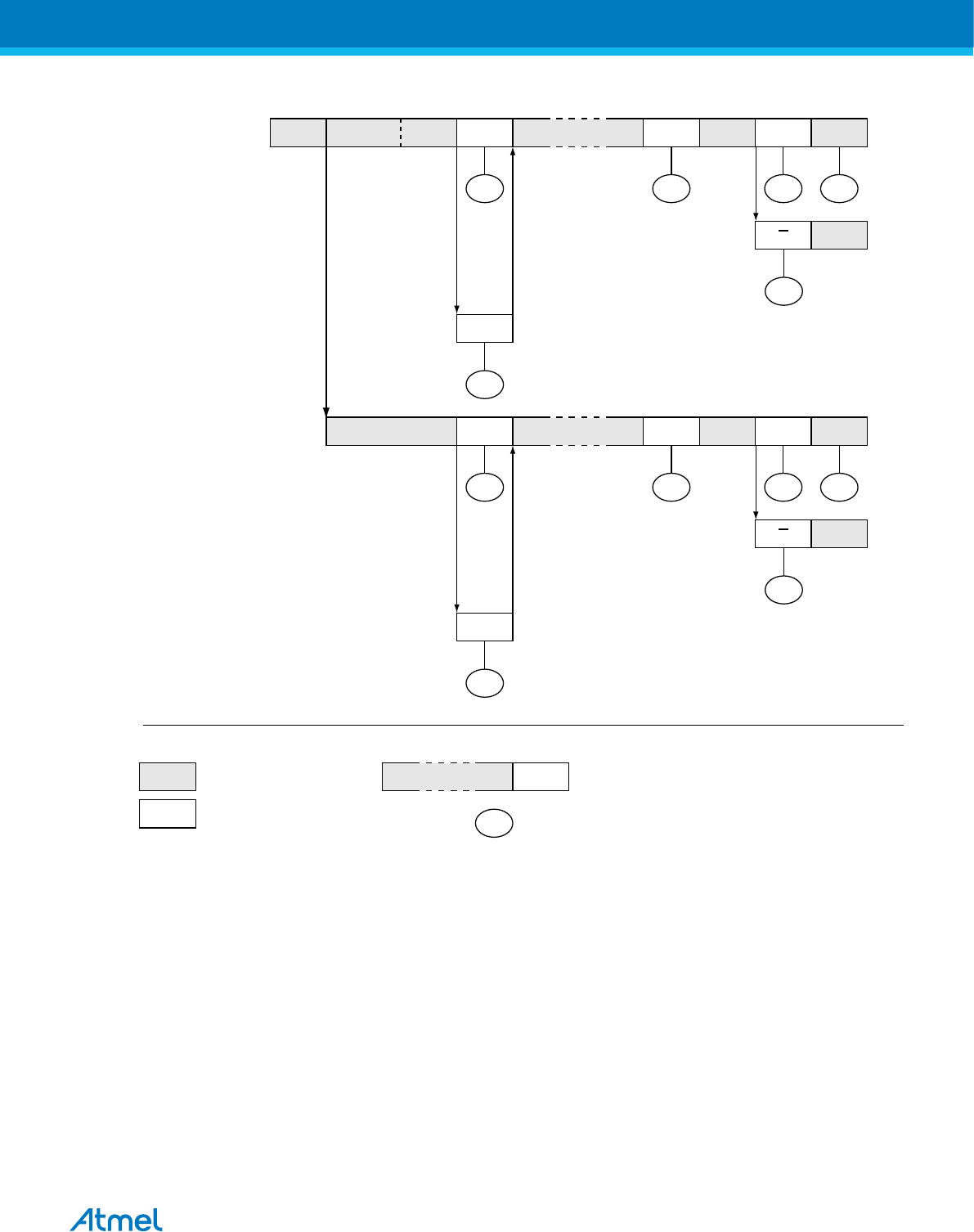
Figure 25-16 Formats and States in the Slave Receiver Mode
S SLA W A DATA A
$60 $80
$88
A
$68
Reception of the o wn
sla v e address and one or
more data b ytes. All are
acknowledged
Last data b yte receiv ed
is not ac kno wledged
Arbitration lost as master
and addressed as sla v e
Reception of the gener al call
address and one or more data
bytes
Last data b yte receiv ed is
not ac knowledged
n
From master to sla v e
From sla v e to master
Any number of data b ytes
and their associated ac kno wledge bits
This n umber (contained in TWSR) corresponds
to a defined state of the 2-Wire Ser ial Bus. The
prescaler bits are z ero or mask ed to z ero
P or SDATA A
$80 $A0
P or SA
A DATA A
$70 $90
$98
A
$78
P or SDATA A
$90 $A0
P or SA
General Call
Arbitration lost as master and
addressed as sla v e b y gener al call
DATA A
25.6.5. Slave Transmitter Mode
In the Slave Transmitter (ST) mode, a number of data bytes are transmitted to a Master Receiver, as in
the figure below. All the status codes mentioned in this section assume that the prescaler bits are zero or
are masked to zero.
Atmel ATmega8A [DATASHEET]
Atmel-8159F-8-bit AVR Microcontroller_Datasheet_Complete-09/2015
231
Figure 25-17 Data Transfer in Slave Transmitter Mode
Device 3 Device n
SD A
SCL
........ R1 R2
VCC
Device 2
MASTER
RECEIVER
Device 1
SLA VE
TRANSMITTER
To initiate the SR mode, the TWI (Slave) Address Register (TWAR) and the TWI Control Register
(TWCR) must be initialized as follows:
The upper seven bits of TWAR are the address to which the 2-wire Serial Interface will respond when
addressed by a Master (TWAR.TWA[6:0]). If the LSB of TWAR is written to TWAR.TWGCI=1, the TWI will
respond to the general call address (0x00), otherwise it will ignore the general call address.
TWCR must hold a value of the type TWCR=0100010x - TWEN must be written to one to enable the TWI.
The TWEA bit must be written to one to enable the acknowledgement of the device’s own slave address
or the general call address. TWSTA and TWSTO must be written to zero.
When TWAR and TWCR have been initialized, the TWI waits until it is addressed by its own slave
address (or the general call address if enabled) followed by the data direction bit. If the direction bit is “1”
(read), the TWI will operate in ST mode, otherwise SR mode is entered. After its own slave address and
the write bit have been received, the TWINT Flag is set and a valid status code can be read from TWSR.
The status code is used to determine the appropriate software action. The appropriate action to be taken
for each status code is detailed in the table below. The ST mode may also be entered if arbitration is lost
while the TWI is in the Master mode (see state 0xB0).
If the TWCR.TWEA bit is written to zero during a transfer, the TWI will transmit the last byte of the
transfer. State 0xC0 or state 0xC8 will be entered, depending on whether the Master Receiver transmits a
NACK or ACK after the final byte. The TWI is switched to the not addressed Slave mode, and will ignore
the Master if it continues the transfer. Thus the Master Receiver receives all '1' as serial data. State 0xC8
is entered if the Master demands additional data bytes (by transmitting ACK), even though the Slave has
transmitted the last byte (TWEA zero and expecting NACK from the Master).
While TWCR.TWEA is zero, the TWI does not respond to its own slave address. However, the 2-wire
Serial Bus is still monitored and address recognition may resume at any time by setting TWEA. This
implies that the TWEA bit may be used to temporarily isolate the TWI from the 2-wire Serial Bus.
In all sleep modes other than Idle mode, the clock system to the TWI is turned off. If the TWEA bit is set,
the interface can still acknowledge its own slave address or the general call address by using the 2-wire
Serial Bus clock as a clock source. The part will then wake up from sleep and the TWI will hold the SCL
clock will low during the wake up and until the TWINT Flag is cleared (by writing '1' to it). Further data
transmission will be carried out as normal, with the AVR clocks running as normal. Observe that if the
AVR is set up with a long start-up time, the SCL line may be held low for a long time, blocking other data
transmissions.
Note: The 2-wire Serial Interface Data Register (TWDR) does not reflect the last byte present on the bus
when waking up from these Sleep modes.
Atmel ATmega8A [DATASHEET]
Atmel-8159F-8-bit AVR Microcontroller_Datasheet_Complete-09/2015
232

Table 25-6 Status Codes for Slave Transmitter Mode
Status
Code
(TWSR)
Prescaler
Bits are 0
Status of the 2-wire Serial
Bus and 2-wire Serial
Interface Hardware
Application Software Response Next Action Taken by TWI Hardware
To/from TWDR To TWCR
STA STO TWI
NT
TWE
A
0xA8 Own SLA+R has been
received;
ACK has been returned
Load data byte or
Load data byte
X
X
0
0
1
1
0
1
Last data byte will be transmitted and NOT ACK
should be received
Data byte will be transmitted and ACK should be
received
0xB0 Arbitration lost in SLA+R/W
as Master; own SLA+R has
been
received; ACK has been
returned
Load data byte or
Load data byte
X
X
0
0
1
1
0
1
Last data byte will be transmitted and NOT ACK
should be received
Data byte will be transmitted and ACK should be
received
0xB8 Data byte in TWDR has
been
transmitted; ACK has been
received
Load data byte or
Load data byte
X
X
0
0
1
1
0
1
Last data byte will be transmitted and NOT ACK
should be received
Data byte will be transmitted and ACK should be
received
0xC0 Data byte in TWDR has
been
transmitted; NOT ACK has
been
received
No TWDR action
or
No TWDR action
or
No TWDR action
or
No TWDR action
0
0
1
1
0
0
0
0
1
1
1
1
0
1
0
1
Switched to the not addressed Slave mode;
no recognition of own SLA or GCA
Switched to the not addressed Slave mode;
own SLA will be recognized;
GCA will be recognized if TWGCE = “1”
Switched to the not addressed Slave mode;
no recognition of own SLA or GCA;
a START condition will be transmitted when the bus
becomes free
Switched to the not addressed Slave mode;
own SLA will be recognized;
GCA will be recognized if TWGCE = “1”; a START
condition will be transmitted when the bus becomes
free
0xC8 Last data byte in TWDR has
been transmitted (TWEA =
“0”); ACK has been received
No TWDR action
or
No TWDR action
or
No TWDR action
or
No TWDR action
0
0
1
1
0
0
0
0
1
1
1
1
0
1
0
1
Switched to the not addressed Slave mode;
no recognition of own SLA or GCA
Switched to the not addressed Slave mode;
own SLA will be recognized;
GCA will be recognized if TWGCE = “1”
Switched to the not addressed Slave mode;
no recognition of own SLA or GCA;
a START condition will be transmitted when the bus
becomes free
Switched to the not addressed Slave mode;
own SLA will be recognized;
GCA will be recognized if TWGCE = “1”; a START
condition will be transmitted when the bus becomes
free
Atmel ATmega8A [DATASHEET]
Atmel-8159F-8-bit AVR Microcontroller_Datasheet_Complete-09/2015
233
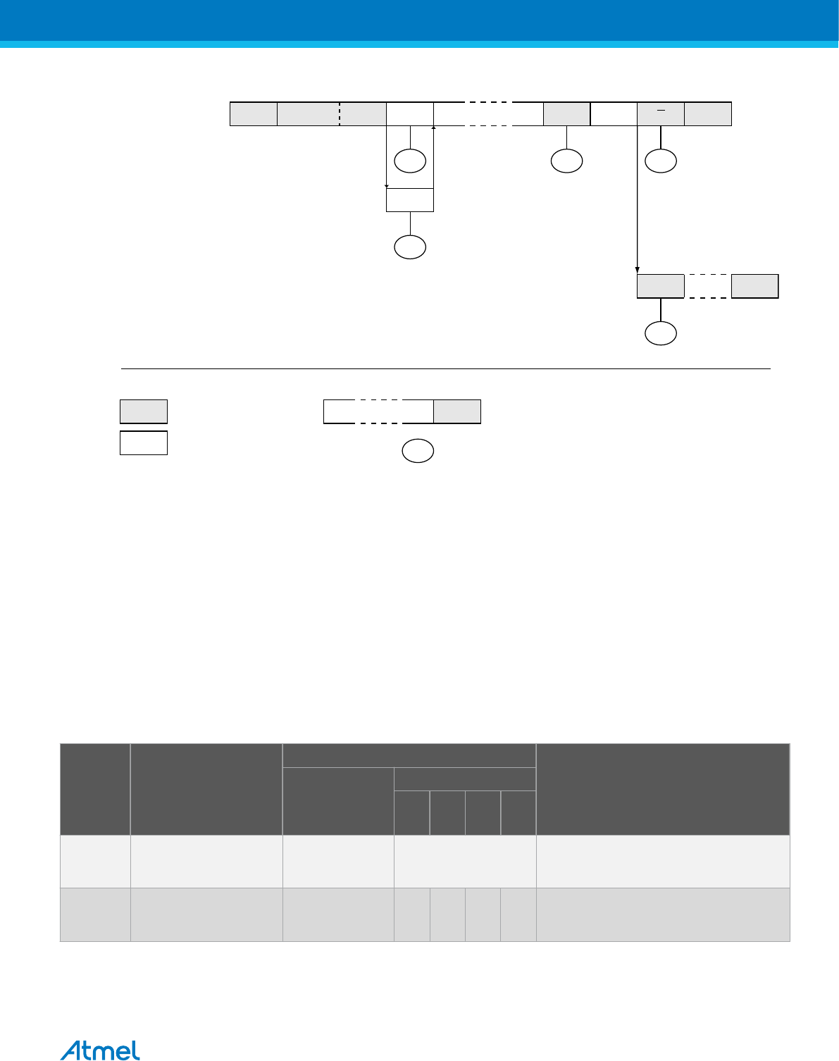
Figure 25-18 Formats and States in the Slave Transmitter Mode
S SLA R A DATA A
$A8 $B8
A
$B0
Reception of the o wn
sla v e address and one or
more data b ytes
Last data b yte tr ansmitted.
Switched to not addressed
slave (TWEA = '0')
Arbitration lost as master
and addressed as sla v e
n
From master to sla v e
From slave to master
Any number of data b ytes
and their associated ac kno wledge bits
This number (contained in TWSR) corresponds
to a defined state of the 2-Wire Ser ial Bus. The
prescaler bits are z ero or mask ed to z ero
P or SDATA
$C0
DATA A
A
$C8
P or SAll 1's
A
25.6.6. Miscellaneous States
There are two status codes that do not correspond to a defined TWI state, see the table below.
Status 0xF8 indicates that no relevant information is available because the TWINT Flag is not set. This
occurs between other states, and when the TWI is not involved in a serial transfer.
Status 0x00 indicates that a bus error has occurred during a Two-wire Serial Bus transfer. A bus error
occurs when a START or STOP condition occurs at an illegal position in the format frame. Examples of
such illegal positions are during the serial transfer of an address byte, a data byte, or an acknowledge bit.
When a bus error occurs, TWINT is set. To recover from a bus error, the TWSTO Flag must set and
TWINT must be cleared by writing a logic one to it. This causes the TWI to enter the not addressed Slave
mode and to clear the TWSTO Flag (no other bits in TWCR are affected). The SDA and SCL lines are
released, and no STOP condition is transmitted.
Table 25-7 Miscellaneous States
Status
Code
(TWSR)
Prescaler
Bits are 0
Status of the 2-wire Serial
Bus and 2-wire Serial
Interface Hardware
Application Software Response Next Action Taken by TWI Hardware
To/from TWDR To TWCR
STA STO TWI
NT
TWE
A
0xF8 No relevant state
information available;
TWINT = “0”
No TWDR action No TWCR action Wait or proceed current transfer
0x00 Bus error due to an illegal
START or STOP condition
No TWDR action 0 1 1 X Only the internal hardware is affected, no STOP
condition is sent on the bus. In all cases, the bus
is released and TWSTO is cleared.
25.6.7. Combining Several TWI Modes
In some cases, several TWI modes must be combined in order to complete the desired action. Consider
for example reading data from a serial EEPROM. Typically, such a transfer involves the following steps:
Atmel ATmega8A [DATASHEET]
Atmel-8159F-8-bit AVR Microcontroller_Datasheet_Complete-09/2015
234
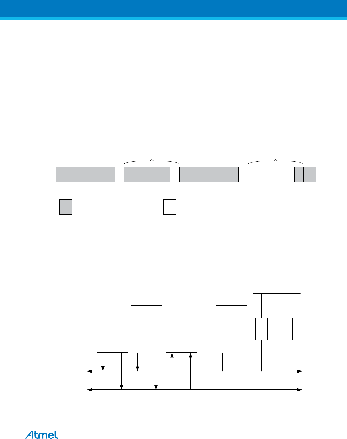
1. The transfer must be initiated.
2. The EEPROM must be instructed what location should be read.
3. The reading must be performed.
4. The transfer must be finished.
Note that data is transmitted both from Master to Slave and vice versa. The Master must instruct the
Slave what location it wants to read, requiring the use of the MT mode. Subsequently, data must be read
from the Slave, implying the use of the MR mode. Thus, the transfer direction must be changed. The
Master must keep control of the bus during all these steps, and the steps should be carried out as an
atomical operation. If this principle is violated in a multimaster system, another Master can alter the data
pointer in the EEPROM between steps 2 and 3, and the Master will read the wrong data location. Such a
change in transfer direction is accomplished by transmitting a REPEATED START between the
transmission of the address byte and reception of the data. After a REPEATED START, the Master keeps
ownership of the bus. The following figure shows the flow in this transfer.
Figure 25-19 Combining Several TWI Modes to Access a Serial EEPROM
Master Transmitter Master Receiv er
S = ST AR T Rs = REPEA TED ST AR T P = ST OP
Transmitted from master to sla v e Transmitted from sla v e to master
S SLA+W A ADDRESS A Rs SLA+R A DATA A P
25.7. Multi-master Systems and Arbitration
If multiple masters are connected to the same bus, transmissions may be initiated simultaneously by one
or more of them. The TWI standard ensures that such situations are handled in such a way that one of
the masters will be allowed to proceed with the transfer, and that no data will be lost in the process. An
example of an arbitration situation is depicted below, where two masters are trying to transmit data to a
Slave Receiver.
Figure 25-20 An Arbitration Example
Device 1
MASTER
TRANSMITTER
Device 2
MASTER
TRANSMITTER
Device 3
SLA VE
RECEIVER
Device n
SD A
SCL
........ R1 R2
VCC
Several different scenarios may arise during arbitration, as described below:
•Two or more masters are performing identical communication with the same Slave. In this case,
neither the Slave nor any of the masters will know about the bus contention.
Atmel ATmega8A [DATASHEET]
Atmel-8159F-8-bit AVR Microcontroller_Datasheet_Complete-09/2015
235
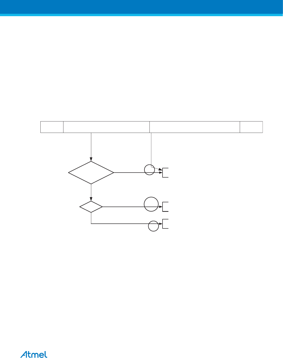
•Two or more masters are accessing the same Slave with different data or direction bit. In this case,
arbitration will occur, either in the READ/WRITE bit or in the data bits. The masters trying to output
a '1' on SDA while another Master outputs a zero will lose the arbitration. Losing masters will switch
to not addressed Slave mode or wait until the bus is free and transmit a new START condition,
depending on application software action.
•Two or more masters are accessing different slaves. In this case, arbitration will occur in the SLA
bits. Masters trying to output a '1' on SDA while another Master outputs a zero will lose the
arbitration. Masters losing arbitration in SLA will switch to Slave mode to check if they are being
addressed by the winning Master. If addressed, they will switch to SR or ST mode, depending on
the value of the READ/WRITE bit. If they are not being addressed, they will switch to not addressed
Slave mode or wait until the bus is free and transmit a new START condition, depending on
application software action.
This is summarized in the next figure. Possible status values are given in circles.
Figure 25-21 Possible Status Codes Caused by Arbitration
Own
Address / General Call
received
Arbitration lost in SLA
TWI bus will be released and not addressed slave mode will be entered
A START condition will be transmitted when the bus becomes free
No
Arbitration lost in Data
Direction
Yes
Write Data byte will be received and NOT ACK will be returned
Data byte will be received and ACK will be returned
Last data byte will be transmitted and NOT ACK should be received
Data byte will be transmitted and ACK should be received
Read
B0
68/78
38
SLASTART Data STOP
25.8. Register Description
Atmel ATmega8A [DATASHEET]
Atmel-8159F-8-bit AVR Microcontroller_Datasheet_Complete-09/2015
236

25.8.1. TWBR – TWI Bit Rate Register
When using the I/O specific commands IN and OUT, the I/O addresses 0x00 - 0x3F must be used. When
addressing I/O Registers as data space using LD and ST instructions, 0x20 must be added to these offset
addresses. The device is a complex microcontroller with more peripheral units than can be supported
within the 64 location reserved in Opcode for the IN and OUT instructions. For the Extended I/O space
from 0x60 in SRAM, only the ST/STS/STD and LD/LDS/LDD instructions can be used.
Name: TWBR
Offset: 0x00
Reset: 0x00
Property:
When addressing I/O Registers as data space the offset address is 0x20
Bit 7 6 5 4 3 2 1 0
TWBR7 TWBR6 TWBR5 TWBR4 TWBR3 TWBR2 TWBR1 TWBR0
Access R/W R/W R/W R/W R/W R/W R/W R/W
Reset 0 0 0 0 0 0 0 0
Bits 7:0 – TWBRn: TWI Bit Rate Register [n = 7:0]
TWBR selects the division factor for the bit rate generator. The bit rate generator is a frequency divider
which generates the SCL clock frequency in the Master modes. See Bit Rate Generator Unit for
calculating bit rates.
Atmel ATmega8A [DATASHEET]
Atmel-8159F-8-bit AVR Microcontroller_Datasheet_Complete-09/2015
237

25.8.2. TWCR – TWI Control Register
When using the I/O specific commands IN and OUT, the I/O addresses 0x00 - 0x3F must be used. When
addressing I/O Registers as data space using LD and ST instructions, 0x20 must be added to these offset
addresses. The device is a complex microcontroller with more peripheral units than can be supported
within the 64 location reserved in Opcode for the IN and OUT instructions. For the Extended I/O space
from 0x60 in SRAM, only the ST/STS/STD and LD/LDS/LDD instructions can be used.
The TWCR is used to control the operation of the TWI. It is used to enable the TWI, to initiate a Master
access by applying a START condition to the bus, to generate a Receiver acknowledge, to generate a
stop condition, and to control halting of the bus while the data to be written to the bus are written to the
TWDR. It also indicates a write collision if data is attempted written to TWDR while the register is
inaccessible.
Name: TWCR
Offset: 0x36
Reset: 0x00
Property:
When addressing I/O Registers as data space the offset address is 0x56
Bit 7 6 5 4 3 2 1 0
TWINT TWEA TWSTA TWSTO TWWC TWEN TWIE
Access R/W R/W R/W R/W R R/W R/W
Reset 0 0 0 0 0 0 0
Bit 7 – TWINT: TWI Interrupt Flag
This bit is set by hardware when the TWI has finished its current job and expects application software
response. If the I-bit in SREG and TWIE in TWCR are set, the MCU will jump to the TWI Interrupt Vector.
While the TWINT Flag is set, the SCL low period is stretched. The TWINT Flag must be cleared by
software by writing a logic one to it.
Note that this flag is not automatically cleared by hardware when executing the interrupt routine. Also
note that clearing this flag starts the operation of the TWI, so all accesses to the TWI Address Register
(TWAR), TWI Status Register (TWSR), and TWI Data Register (TWDR) must be complete before clearing
this flag.
Bit 6 – TWEA: TWI Enable Acknowledge
The TWEA bit controls the generation of the acknowledge pulse. If the TWEA bit is written to one, the
ACK pulse is generated on the TWI bus if the following conditions are met:
1. The device’s own slave address has been received.
2. A general call has been received, while the TWGCE bit in the TWAR is set.
3. A data byte has been received in Master Receiver or Slave Receiver mode.
By writing the TWEA bit to zero, the device can be virtually disconnected from the 2-wire Serial Bus
temporarily. Address recognition can then be resumed by writing the TWEA bit to one again.
Bit 5 – TWSTA: TWI START Condition
The application writes the TWSTA bit to one when it desires to become a Master on the 2-wire Serial Bus.
The TWI hardware checks if the bus is available, and generates a START condition on the bus if it is free.
However, if the bus is not free, the TWI waits until a STOP condition is detected, and then generates a
new START condition to claim the bus Master status. TWSTA must be cleared by software when the
START condition has been transmitted.
Atmel ATmega8A [DATASHEET]
Atmel-8159F-8-bit AVR Microcontroller_Datasheet_Complete-09/2015
238

Bit 4 – TWSTO: TWI STOP Condition
Writing the TWSTO bit to one in Master mode will generate a STOP condition on the 2-wire Serial Bus.
When the STOP condition is executed on the bus, the TWSTO bit is cleared automatically. In Slave
mode, setting the TWSTO bit can be used to recover from an error condition. This will not generate a
STOP condition, but the TWI returns to a well-defined unaddressed Slave mode and releases the SCL
and SDA lines to a high impedance state.
Bit 3 – TWWC: TWI Write Collision Flag
The TWWC bit is set when attempting to write to the TWI Data Register – TWDR when TWINT is low.
This flag is cleared by writing the TWDR Register when TWINT is high.
Bit 2 – TWEN: TWI Enable
The TWEN bit enables TWI operation and activates the TWI interface. When TWEN is written to one, the
TWI takes control over the I/O pins connected to the SCL and SDA pins, enabling the slew-rate limiters
and spike filters. If this bit is written to zero, the TWI is switched off and all TWI transmissions are
terminated, regardless of any ongoing operation.
Bit 0 – TWIE: TWI Interrupt Enable
When this bit is written to one, and the I-bit in SREG is set, the TWI interrupt request will be activated for
as long as the TWINT Flag is high.
Atmel ATmega8A [DATASHEET]
Atmel-8159F-8-bit AVR Microcontroller_Datasheet_Complete-09/2015
239
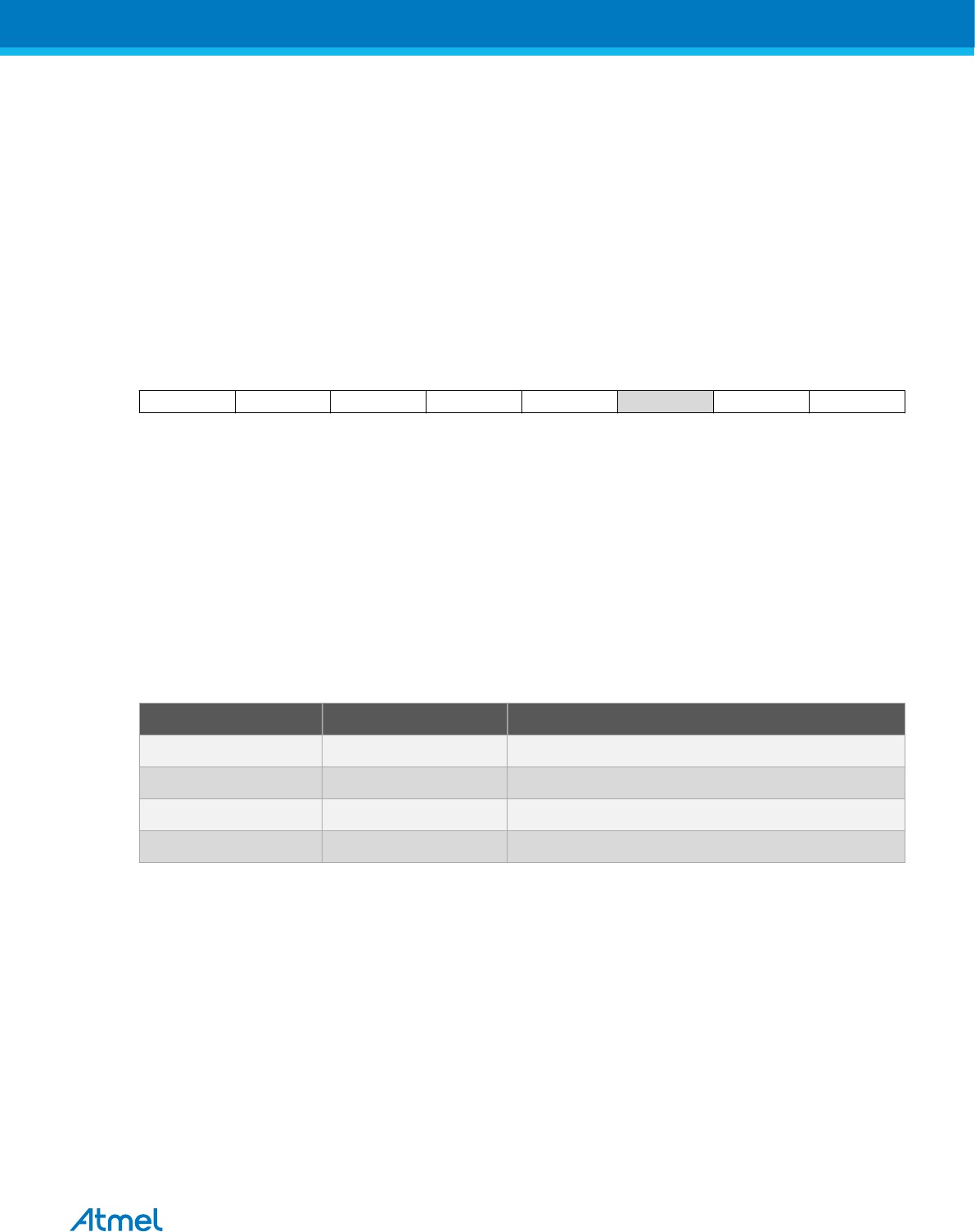
25.8.3. TWSR – TWI Status Register
When using the I/O specific commands IN and OUT, the I/O addresses 0x00 - 0x3F must be used. When
addressing I/O Registers as data space using LD and ST instructions, 0x20 must be added to these offset
addresses. The device is a complex microcontroller with more peripheral units than can be supported
within the 64 location reserved in Opcode for the IN and OUT instructions. For the Extended I/O space
from 0x60 in SRAM, only the ST/STS/STD and LD/LDS/LDD instructions can be used.
Name: TWSR
Offset: 0x01
Reset: 0xF8
Property:
When addressing I/O Registers as data space the offset address is 0x21
Bit 7 6 5 4 3 2 1 0
TWS4 TWS3 TWS2 TWS1 TWS0 TWPS1 TWPS0
Access R R R R R R/W R/W
Reset 0 0 0 0 1 0 0
Bits 7:3 – TWSn: TWI Status Bit 7 [n = 7:3]
The TWS[7:3] reflect the status of the TWI logic and the 2-wire Serial Bus. The different status codes are
described later in this section. Note that the value read from TWSR contains both the 5-bit status value
and the 2-bit prescaler value. The application designer should mask the prescaler bits to zero when
checking the Status bits. This makes status checking independent of prescaler setting. This approach is
used in this datasheet, unless otherwise noted.
Bits 1:0 – TWPSn: TWI Prescaler [n = 1:0]
These bits can be read and written, and control the bit rate prescaler.
Table 25-8 TWI Bit Rate Prescaler
TWPS1 TWPS0 Prescaler Value
0 0 1
0 1 4
1 0 16
1 1 64
To calculate bit rates, refer to Bit Rate Generator Unit. The value of TWPS1:0 is used in the equation.
Atmel ATmega8A [DATASHEET]
Atmel-8159F-8-bit AVR Microcontroller_Datasheet_Complete-09/2015
240

25.8.4. TWDR – TWI Data Register
When using the I/O specific commands IN and OUT, the I/O addresses 0x00 - 0x3F must be used. When
addressing I/O Registers as data space using LD and ST instructions, 0x20 must be added to these offset
addresses. The device is a complex microcontroller with more peripheral units than can be supported
within the 64 location reserved in Opcode for the IN and OUT instructions. For the Extended I/O space
from 0x60 in SRAM, only the ST/STS/STD and LD/LDS/LDD instructions can be used.
In Transmit mode, TWDR contains the next byte to be transmitted. In Receive mode, the TWDR contains
the last byte received. It is writable while the TWI is not in the process of shifting a byte. This occurs when
the TWI Interrupt Flag (TWINT) is set by hardware. Note that the Data Register cannot be initialized by
the user before the first interrupt occurs. The data in TWDR remains stable as long as TWINT is set.
While data is shifted out, data on the bus is simultaneously shifted in. TWDR always contains the last
byte present on the bus, except after a wake up from a sleep mode by the TWI interrupt. In this case, the
contents of TWDR is undefined. In the case of a lost bus arbitration, no data is lost in the transition from
Master to Slave. Handling of the ACK bit is controlled automatically by the TWI logic, the CPU cannot
access the ACK bit directly.
Name: TWDR
Offset: 0x03
Reset: 0xFF
Property:
When addressing I/O Registers as data space the offset address is 0x23
Bit 7 6 5 4 3 2 1 0
TWD7 TWD6 TWD5 TWD4 TWD3 TWD2 TWD1 TWD0
Access R/W R/W R/W R/W R/W R/W R/W R/W
Reset 0 0 0 0 0 0 0 1
Bits 7:0 – TWDn: TWI Data [n = 7:0]
These eight bits constitute the next data byte to be transmitted, or the latest data byte received on the 2-
wire Serial Bus.
Atmel ATmega8A [DATASHEET]
Atmel-8159F-8-bit AVR Microcontroller_Datasheet_Complete-09/2015
241

25.8.5. TWAR – TWI (Slave) Address Register
When using the I/O specific commands IN and OUT, the I/O addresses 0x00 - 0x3F must be used. When
addressing I/O Registers as data space using LD and ST instructions, 0x20 must be added to these offset
addresses. The device is a complex microcontroller with more peripheral units than can be supported
within the 64 location reserved in Opcode for the IN and OUT instructions. For the Extended I/O space
from 0x60 in SRAM, only the ST/STS/STD and LD/LDS/LDD instructions can be used.
The TWAR should be loaded with the 7-bit Slave address (in the seven most significant bits of TWAR) to
which the TWI will respond when programmed as a Slave Transmitter or Receiver, and not needed in the
Master modes. In multimaster systems, TWAR must be set in masters which can be addressed as Slaves
by other Masters.
The LSB of TWAR is used to enable recognition of the general call address (0x00). There is an
associated address comparator that looks for the slave address (or general call address if enabled) in the
received serial address. If a match is found, an interrupt request is generated.
Name: TWAR
Offset: 0x02
Reset: 0x7F
Property:
When addressing I/O Registers as data space the offset address is 0x22
Bit 7 6 5 4 3 2 1 0
TWA6 TWA5 TWA4 TWA3 TWA2 TWA1 TWA0 TWGCE
Access R/W R/W R/W R/W R/W R/W R/W R/W
Reset 0 0 0 0 0 0 1 0
Bits 7:1 – TWAn: TWI (Slave) Address [n = 6:0]
These seven bits constitute the slave address of the TWI unit.
Bit 0 – TWGCE: TWI General Call Recognition Enable Bit
If set, this bit enables the recognition of a General Call given over the Two-wire Serial Bus.
Atmel ATmega8A [DATASHEET]
Atmel-8159F-8-bit AVR Microcontroller_Datasheet_Complete-09/2015
242
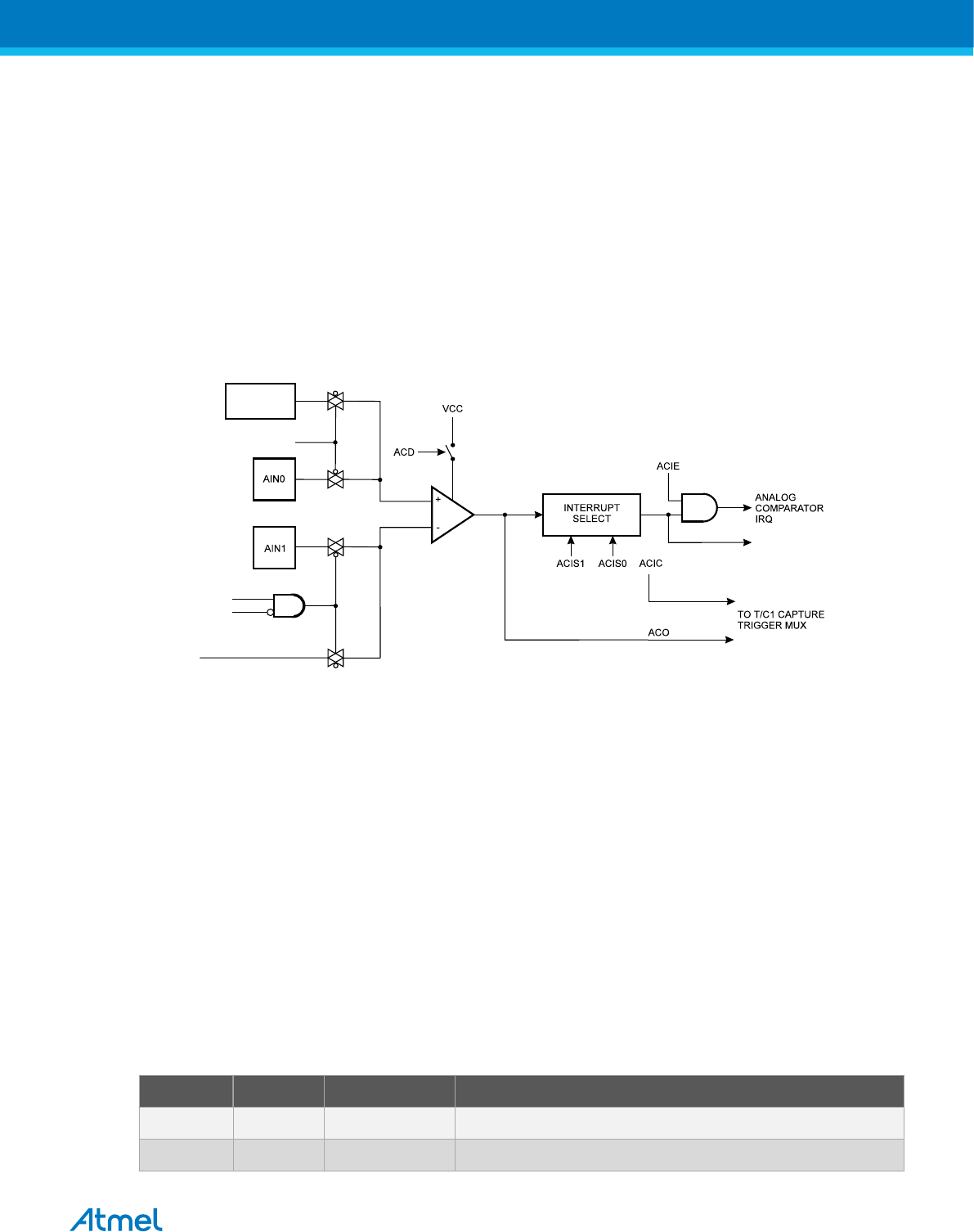
26. Analog Comparator
26.1. Overview
The Analog Comparator compares the input values on the positive pin AIN0 and negative pin AIN1. When
the voltage on the positive pin AIN0 is higher than the voltage on the negative pin AIN1, the Analog
Comparator Output, ACO, is set. The comparator’s output can be set to trigger the Timer/Counter1 Input
Capture function. In addition, the comparator can trigger a separate interrupt, exclusive to the Analog
Comparator. The user can select Interrupt triggering on comparator output rise, fall or toggle. A block
diagram of the comparator and its surrounding logic is shown in the figure below.
Figure 26-1 Analog Comparator Block Diagram(2)
ACBG
BANDGAP
REFERENCE
ADC MULTIPLEXER
OUTPUT
ACME
ADEN
(1)
Note:
1. See Table Analog Comparator Multiplexed Input in next section.
2. Refer to the Pin Configuration and the Port D Pins Alternate Functions Table.
Related Links
Pin Configurations on page 13
Alternate Functions of Port D on page 88
26.2. Analog Comparator Multiplexed Input
It is possible to select any of the ADC7:0 pins to replace the negative input to the Analog Comparator.
The ADC multiplexer is used to select this input, and consequently the ADC must be switched off to utilize
this feature. If the Analog Comparator Multiplexer Enable bit (ACME in SFIOR) is set and the ADC is
switched off (ADEN in ADCSRA is zero), MUX2:0 in ADMUX select the input pin to replace the negative
input to the Analog Comparator, as shown in the table below. If ACME is cleared or ADEN is set, AIN1 is
applied to the negative input to the Analog Comparator.
Table 26-1 Analog Comparator Multiplexed Input(1)
ACME ADEN MUX[2:0] Analog Comparator Negative Input
0 x xxx AIN1
1 1 xxx AIN1
Atmel ATmega8A [DATASHEET]
Atmel-8159F-8-bit AVR Microcontroller_Datasheet_Complete-09/2015
243

ACME ADEN MUX[2:0] Analog Comparator Negative Input
1 0 000 ADC0
1 0 001 ADC1
1 0 010 ADC2
1 0 011 ADC3
1 0 100 ADC4
1 0 101 ADC5
1 0 110 ADC6
1 0 111 ADC7
Note: 1. ADC7:6 are only available in TQFP and QFN/MLF Package.
26.3. Register Description
Atmel ATmega8A [DATASHEET]
Atmel-8159F-8-bit AVR Microcontroller_Datasheet_Complete-09/2015
244
26.3.1. SFIOR – Analog Comparator Control and Status Register
When using the I/O specific commands IN and OUT, the I/O addresses 0x00 - 0x3F must be used. When
addressing I/O Registers as data space using LD and ST instructions, 0x20 must be added to these offset
addresses. The device is a complex microcontroller with more peripheral units than can be supported
within the 64 location reserved in Opcode for the IN and OUT instructions. For the Extended I/O space
from 0x60 in SRAM, only the ST/STS/STD and LD/LDS/LDD instructions can be used.
Name: SFIOR
Offset: 0x30
Reset: N/A
Property:
When addressing I/O Registers as data space the offset address is 0x50
Bit 7 6 5 4 3 2 1 0
ACME
Access R/W
Reset 0
Bit 3 – ACME: Analog Comparator Multiplexer Enable
When this bit is written logic one and the ADC is switched off (ADEN in ADCSRA is zero), the ADC
multiplexer selects the negative input to the Analog Comparator. When this bit is written logic zero, AIN1
is applied to the negative input of the Analog Comparator. For a detailed description of this bit, see
Analog Comparator Multiplexed Input.
Atmel ATmega8A [DATASHEET]
Atmel-8159F-8-bit AVR Microcontroller_Datasheet_Complete-09/2015
245

26.3.2. ACSR – Analog Comparator Control and Status Register
When using the I/O specific commands IN and OUT, the I/O addresses 0x00 - 0x3F must be used. When
addressing I/O Registers as data space using LD and ST instructions, 0x20 must be added to these offset
addresses. The device is a complex microcontroller with more peripheral units than can be supported
within the 64 location reserved in Opcode for the IN and OUT instructions. For the Extended I/O space
from 0x60 in SRAM, only the ST/STS/STD and LD/LDS/LDD instructions can be used.
Name: ACSR
Offset: 0x08
Reset: N/A
Property:
When addressing I/O Registers as data space the offset address is 0x28
Bit 7 6 5 4 3 2 1 0
ACD ACBG ACO ACI ACIE ACIC ACIS1 ACIS0
Access R/W R/W R R/W R/W R/W R/W R/W
Reset 0 0 a 0 0 0 0 0
Bit 7 – ACD: Analog Comparator Disable
When this bit is written logic one, the power to the Analog Comparator is switched off. This bit can be set
at any time to turn off the Analog Comparator. This will reduce power consumption in Active and Idle
mode. When changing the ACD bit, the Analog Comparator Interrupt must be disabled by clearing the
ACIE bit in ACSR. Otherwise an interrupt can occur when the bit is changed.
Bit 6 – ACBG: Analog Comparator Bandgap Select
When this bit is set, a fixed bandgap reference voltage replaces the positive input to the Analog
Comparator. When this bit is cleared, AIN0 is applied to the positive input of the Analog Comparator.
Refer to Internal Voltage Reference in System Control and Reset.
Bit 5 – ACO: Analog Comparator Output
The output of the Analog Comparator is synchronized and then directly connected to ACO. The
synchronization introduces a delay of 1 - 2 clock cycles.
Bit 4 – ACI: Analog Comparator Interrupt Flag
This bit is set by hardware when a comparator output event triggers the interrupt mode defined by ACIS1
and ACIS0. The Analog Comparator interrupt routine is executed if the ACIE bit is set and the I-bit in
SREG is set. ACI is cleared by hardware when executing the corresponding interrupt handling vector.
Alternatively, ACI is cleared by writing a logic one to the flag.
Bit 3 – ACIE: Analog Comparator Interrupt Enable
When the ACIE bit is written logic one and the I-bit in the Status Register is set, the Analog Comparator
interrupt is activated. When written logic zero, the interrupt is disabled.
Bit 2 – ACIC: Analog Comparator Input Capture Enable
When written logic one, this bit enables the input capture function in Timer/Counter1 to be triggered by
the Analog Comparator. The comparator output is in this case directly connected to the input capture
front-end logic, making the comparator utilize the noise canceler and edge select features of the Timer/
Counter1 Input Capture interrupt. When written logic zero, no connection between the Analog
Comparator and the input capture function exists. To make the comparator trigger the Timer/Counter1
Input Capture interrupt, the ICIE1 bit in the Timer Interrupt Mask Register (TIMSK1) must be set.
Atmel ATmega8A [DATASHEET]
Atmel-8159F-8-bit AVR Microcontroller_Datasheet_Complete-09/2015
246

Bits 1:0 – ACISn: Analog Comparator Interrupt Mode Select [n = 1:0]
These bits determine which comparator events that trigger the Analog Comparator interrupt.
Table 26-2 ACIS[1:0] Settings
ACIS1 ACIS0 Interrupt Mode
0 0 Comparator Interrupt on Output Toggle.
0 1 Reserved
1 0 Comparator Interrupt on Falling Output Edge.
1 1 Comparator Interrupt on Rising Output Edge.
When changing the ACIS1/ACIS0 bits, the Analog Comparator Interrupt must be disabled by clearing its
Interrupt Enable bit in the ACSR Register. Otherwise an interrupt can occur when the bits are changed.
Atmel ATmega8A [DATASHEET]
Atmel-8159F-8-bit AVR Microcontroller_Datasheet_Complete-09/2015
247

27. ADC - Analog to Digital Converter
27.1. Features
•10-bit Resolution
•0.5LSB Integral Non-Linearity
•±2LSB Absolute Accuracy
•13 - 260μs Conversion Time
•Up to 15kSPS at Maximum Resolution
•Six Multiplexed Single Ended Input Channels
•Two Additional Multiplexed Single Ended Input Channels (TQFP and QFN/MLF Package only)
•Optional Left Adjustment for ADC Result Readout
•0 - VCC ADC Input Voltage Range
•Selectable 2.56V ADC Reference Voltage
•Free Running or Single Conversion Mode
•Interrupt on ADC Conversion Complete
•Sleep Mode Noise Canceler
27.2. Overview
The ATmega8A features a 10-bit successive approximation ADC. The ADC is connected to an 8-channel
Analog Multiplexer which allows eight single-ended voltage inputs constructed from the pins of Port C.
The single-ended voltage inputs refer to 0V (GND).
The ADC contains a Sample and Hold circuit which ensures that the input voltage to the ADC is held at a
constant level during conversion. A block diagram of the ADC is shown below.
The ADC has a separate analog supply voltage pin, AVCC. AVCC must not differ more than ±0.3V from
VCC. See section ADC Noise Canceler on page 253 on how to connect this pin.
Internal reference voltages of nominally 2.56V or AVCC are provided On-chip. The voltage reference may
be externally decoupled at the AREF pin by a capacitor for better noise performance.
Atmel ATmega8A [DATASHEET]
Atmel-8159F-8-bit AVR Microcontroller_Datasheet_Complete-09/2015
248
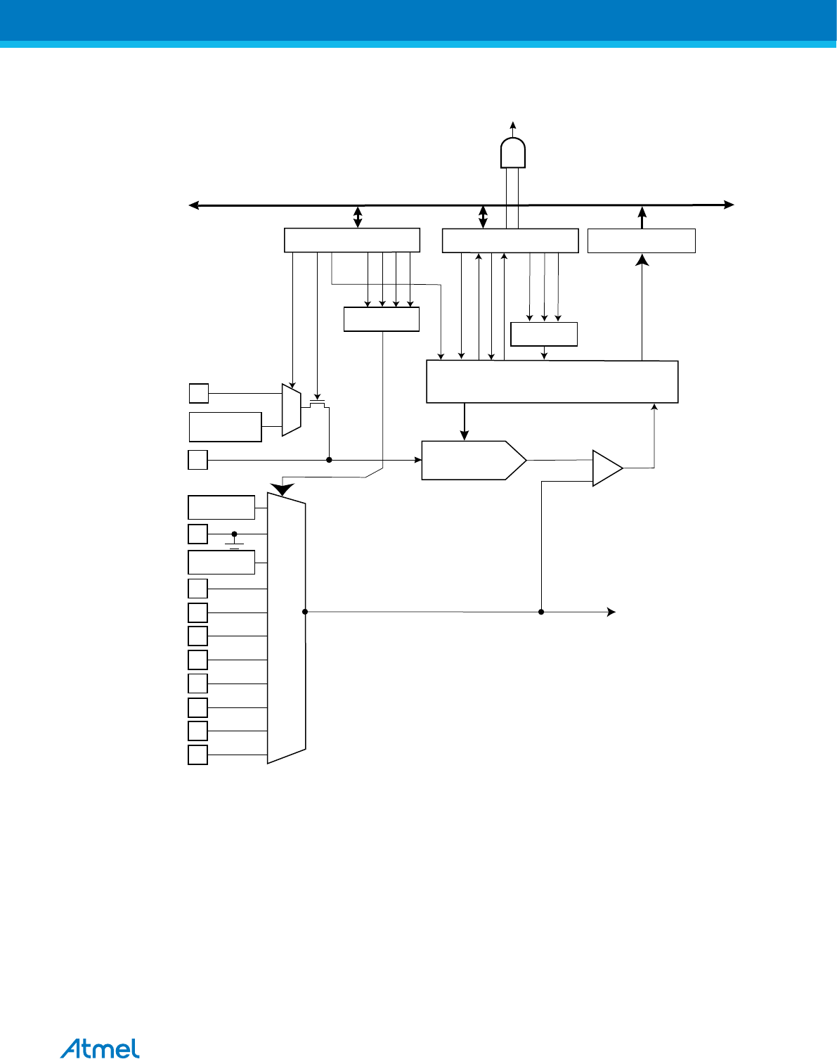
Figure 27-1 Analog to Digital Converter Block Schematic Operation
ADC CONVERSION
COMPLETE IRQ
8-BIT DATA BUS
15 0
ADC MULTIPLEXER
SELECT (ADMUX) ADC CTRL. & ST ATUS
REGISTER (ADCSRA) ADC DATA REGISTER
(ADCH/ADCL)
MUX2
ADIE
ADFR
ADSC
ADEN
ADIF ADIF
MUX1
MUX0
ADPS0
ADPS1
ADPS2
MUX3
CONVERSION LOGIC
10-BIT DAC
+
-
SAMPLE & HOLD
COMPARATOR
INTERNAL 1.1V
REFERENCE
MUX DECODER
AVCC
ADC7
ADC6
ADC5
ADC4
ADC3
ADC2
ADC1
ADC0
REFS0
REFS1
ADLAR
CHANNEL SELECTION
ADC[9:0]
ADC MULTIPLEXER
OUTPUT
AREF
BANDGAP
REFERENCE
PRESCALER
GND
INPUT
MUX
TEMPERATURE
SENSOR
The ADC converts an analog input voltage to a 10-bit digital value through successive approximation. The
minimum value represents GND and the maximum value represents the voltage on the AREF pin minus
1LSB. Optionally, AVCC or an internal 2.56V reference voltage may be connected to the AREF pin by
writing to the REFSn bits in the ADMUX Register. The internal voltage reference may thus be decoupled
by an external capacitor at the AREF pin to improve noise immunity.
The analog input channel is selected by writing to the MUX bits in ADMUX. Any of the ADC input pins, as
well as GND and a fixed bandgap voltage reference, can be selected as single ended inputs to the ADC.
The ADC is enabled by setting the ADC Enable bit, ADEN in ADCSRA. Voltage reference and input
channel selections will not go into effect until ADEN is set. The ADC does not consume power when
ADEN is cleared, so it is recommended to switch off the ADC before entering power saving sleep modes.
Atmel ATmega8A [DATASHEET]
Atmel-8159F-8-bit AVR Microcontroller_Datasheet_Complete-09/2015
249
The ADC generates a 10-bit result which is presented in the ADC Data Registers, ADCH and ADCL. By
default, the result is presented right adjusted, but can optionally be presented left adjusted by setting the
ADLAR bit in ADMUX.
If the result is left adjusted and no more than 8-bit precision is required, it is sufficient to read ADCH.
Otherwise, ADCL must be read first, then ADCH, to ensure that the content of the Data Registers belongs
to the same conversion. Once ADCL is read, ADC access to Data Registers is blocked. This means that if
ADCL has been read, and a conversion completes before ADCH is read, neither register is updated and
the result from the conversion is lost. When ADCH is read, ADC access to the ADCH and ADCL
Registers is re-enabled.
The ADC has its own interrupt which can be triggered when a conversion completes. When ADC access
to the Data Registers is prohibited between reading of ADCH and ADCL, the interrupt will trigger even if
the result is lost.
27.3. Starting a Conversion
A single conversion is started by writing a logical one to the ADC Start Conversion bit, ADSC. This bit
stays high as long as the conversion is in progress and will be cleared by hardware when the conversion
is completed. If a different data channel is selected while a conversion is in progress, the ADC will finish
the current conversion before performing the channel change.
In Free Running mode, the ADC is constantly sampling and updating the ADC Data Register. Free
Running mode is selected by writing the ADFR bit in ADCSRA to one. The first conversion must be
started by writing a logical one to the ADSC bit in ADCSRA. In this mode the ADC will perform successive
conversions independently of whether the ADC Interrupt Flag, ADIF is cleared or not.
27.4. Prescaling and Conversion Timing
Figure 27-2 ADC Prescaler
7-BIT ADC PRESCALER
ADC CLOCK SOURCE
CK
ADPS0
ADPS1
ADPS2
CK/128
CK/2
CK/4
CK/8
CK/16
CK/32
CK/64
Reset
ADEN
START
By default, the successive approximation circuitry requires an input clock frequency between 50kHz and
200kHz to get maximum resolution. If a lower resolution than 10 bits is needed, the input clock frequency
to the ADC can be higher than 200kHz to get a higher sample rate.
The ADC module contains a prescaler, which generates an acceptable ADC clock frequency from any
CPU frequency above 100kHz. The prescaling is set by the ADPS bits in ADCSRA. The prescaler starts
counting from the moment the ADC is switched on by setting the ADEN bit in ADCSRA. The prescaler
keeps running for as long as the ADEN bit is set, and is continuously reset when ADEN is low.
When initiating a single ended conversion by setting the ADSC bit in ADCSRA, the conversion starts at
the following rising edge of the ADC clock cycle. A normal conversion takes 13 ADC clock cycles. The
Atmel ATmega8A [DATASHEET]
Atmel-8159F-8-bit AVR Microcontroller_Datasheet_Complete-09/2015
250
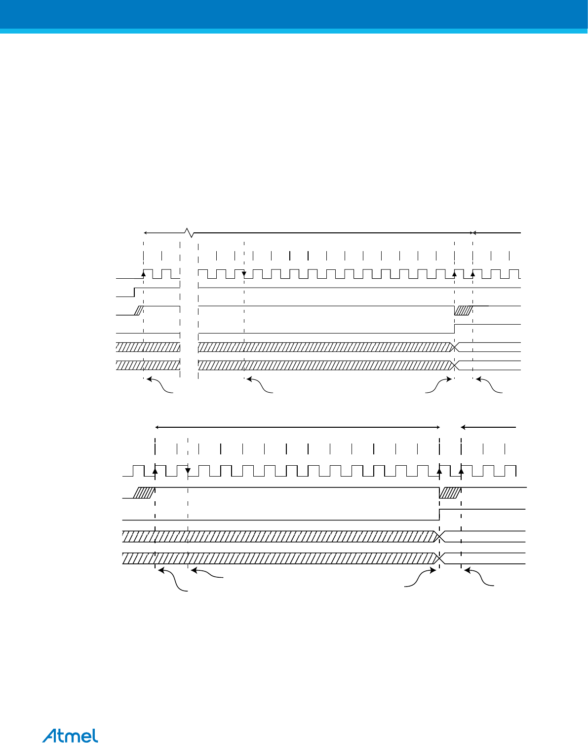
first conversion after the ADC is switched on (ADEN in ADCSRA is set) takes 25 ADC clock cycles in
order to initialize the analog circuitry.
The actual sample-and-hold takes place 1.5 ADC clock cycles after the start of a normal conversion and
13.5 ADC clock cycles after the start of an first conversion. When a conversion is complete, the result is
written to the ADC Data Registers, and ADIF is set. In single conversion mode, ADSC is cleared
simultaneously. The software may then set ADSC again, and a new conversion will be initiated on the first
rising ADC clock edge.
In Free Running mode, a new conversion will be started immediately after the conversion completes,
while ADSC remains high. For a summary of conversion times, see Analog to Digital Converter Block
Schematic Operation.
Figure 27-3 ADC Timing Diagram, First Conversion (Single Conversion Mode)
Sign and MSB of Result
LSB of Result
ADC Clock
ADSC
Sample and Hold
ADIF
ADCH
ADCL
Cycle Number
ADEN
1 2 12 13 14 15 16 17 18 19 20 21 22 23 24 25 1 2
First Conversion Next
Conversion
3
MUX and REFS
Update
MUX and REFS
Update
Conversion
Complete
Figure 27-4 ADC Timing Diagram, Single Conversion
12 3 4 5 6 7 8 9 10 11 12 13
Sign and MSB of Result
LSB of Result
ADC Clock
ADSC
ADIF
ADCH
ADCL
Cycle Number 1 2
One Conversion Next Conversion
3
Sample and Hold
MUX and REFS
Update
Conversion
Complete
MUX and REFS
Update
Atmel ATmega8A [DATASHEET]
Atmel-8159F-8-bit AVR Microcontroller_Datasheet_Complete-09/2015
251
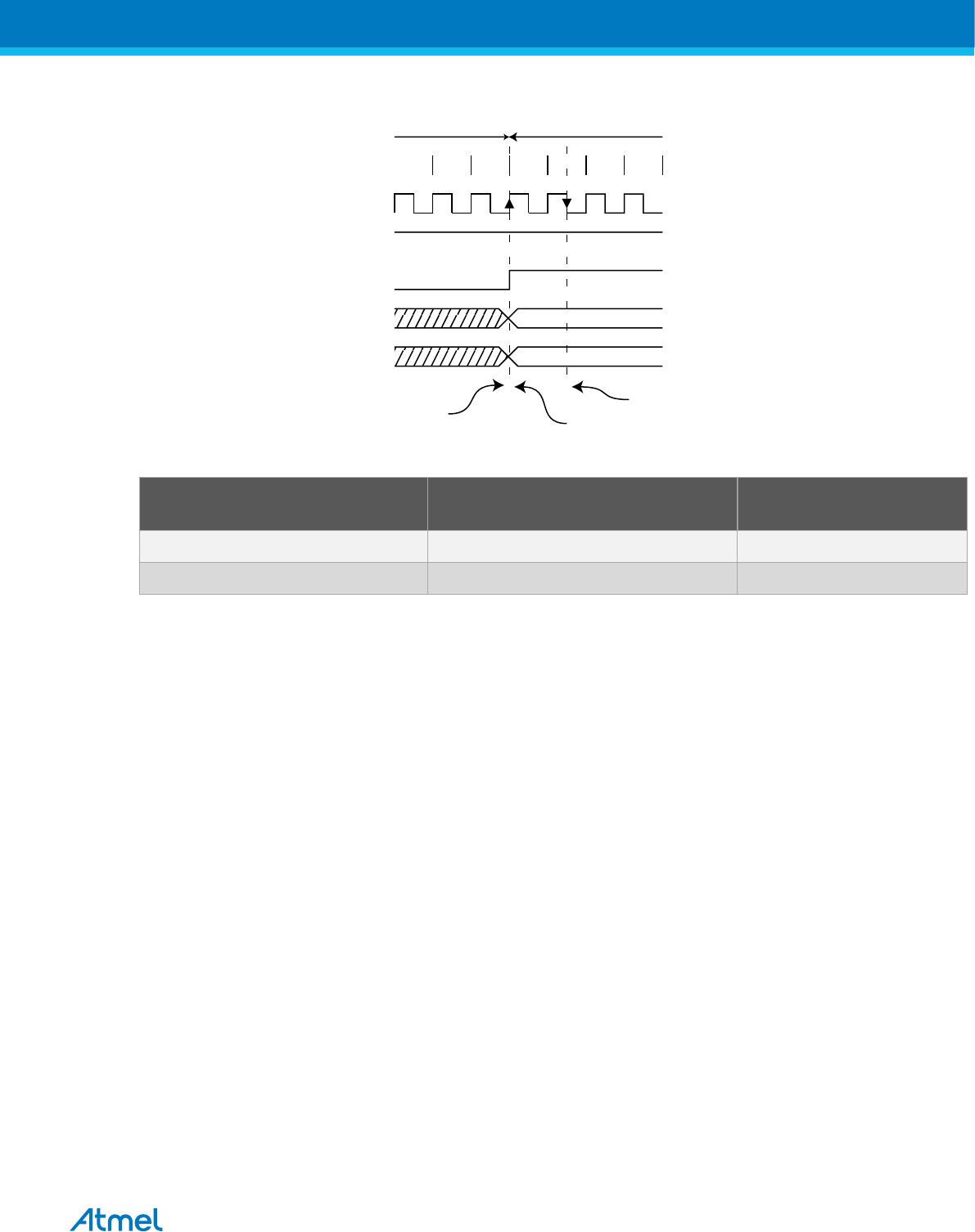
Figure 27-5 ADC Timing Diagram, Free Running Conversion
11 12 13
Sign and MSB of Result
LSB of Result
ADC Clock
ADSC
ADIF
ADCH
ADCL
Cycle Number 12
One Conversion Next Conversion
3 4
Conversion
Complete
Sample and Hold
MUX and REFS
Update
Table 27-1 ADC Conversion Time
Condition Sample & Hold
(Cycles from Start of Conversion)
Conversion Time
(Cycles)
Extended conversion 13.5 25
Normal conversions, single ended 1.5 13
27.5. Changing Channel or Reference Selection
The MUXn and REFS1:0 bits in the ADMUX Register are single buffered through a temporary register to
which the CPU has random access. This ensures that the channels and reference selection only takes
place at a safe point during the conversion. The channel and reference selection is continuously updated
until a conversion is started. Once the conversion starts, the channel and reference selection is locked to
ensure a sufficient sampling time for the ADC. Continuous updating resumes in the last ADC clock cycle
before the conversion completes (ADIF in ADCSRA is set). Note that the conversion starts on the
following rising ADC clock edge after ADSC is written. The user is thus advised not to write new channel
or reference selection values to ADMUX until one ADC clock cycle after ADSC is written.
If both ADFR and ADEN is written to one, an interrupt event can occur at any time. If the ADMUX
Register is changed in this period, the user cannot tell if the next conversion is based on the old or the
new settings. ADMUX can be safely updated in the following ways:
1. When ADFR or ADEN is cleared.
2. During conversion, minimum one ADC clock cycle after the trigger event.
3. After a conversion, before the Interrupt Flag used as trigger source is cleared.
When updating ADMUX in one of these conditions, the new settings will affect the next ADC conversion.
27.5.1. ADC Input Channels
When changing channel selections, the user should observe the following guidelines to ensure that the
correct channel is selected:
•In Single Conversion mode, always select the channel before starting the conversion. The channel
selection may be changed one ADC clock cycle after writing one to ADSC. However, the simplest
method is to wait for the conversion to complete before changing the channel selection.
Atmel ATmega8A [DATASHEET]
Atmel-8159F-8-bit AVR Microcontroller_Datasheet_Complete-09/2015
252

•In Free Running mode, always select the channel before starting the first conversion. The channel
selection may be changed one ADC clock cycle after writing one to ADSC. However, the simplest
method is to wait for the first conversion to complete, and then change the channel selection. Since
the next conversion has already started automatically, the next result will reflect the previous
channel selection. Subsequent conversions will reflect the new channel selection. The user is
advised not to write new channel or reference selection values during Free Running mode.
27.5.2. ADC Voltage Reference
The reference voltage for the ADC (VREF) indicates the conversion range for the ADC. Single ended
channels that exceed VREF will result in codes close to 0x3FF. VREF can be selected as either AVCC,
internal 2.56V reference, or external AREF pin.
AVCC is connected to the ADC through a passive switch. The internal 2.56V reference is generated from
the internal bandgap reference (VBG) through an internal amplifier. In either case, the external AREF pin
is directly connected to the ADC, and the reference voltage can be made more immune to noise by
connecting a capacitor between the AREF pin and ground. VREF can also be measured at the AREF pin
with a high impedance voltmeter. Note that VREF is a high impedance source, and only a capacitive load
should be connected in a system.
If the user has a fixed voltage source connected to the AREF pin, the user may not use the other
reference voltage options in the application, as they will be shorted to the external voltage. If no external
voltage is applied to the AREF pin, the user may switch between AVCC and 2.56V as reference selection.
The first ADC conversion result after switching reference voltage source may be inaccurate, and the user
is advised to discard this result.
27.6. ADC Noise Canceler
The ADC features a noise canceler that enables conversion during sleep mode to reduce noise induced
from the CPU core and other I/O peripherals. The noise canceler can be used with ADC Noise Reduction
and Idle mode. To make use of this feature, the following procedure should be used:
1. Make sure that the ADC is enabled and is not busy converting. Single Conversion mode must be
selected and the ADC conversion complete interrupt must be enabled.
2. Enter ADC Noise Reduction mode (or Idle mode). The ADC will start a conversion once the CPU
has been halted.
3. If no other interrupts occur before the ADC conversion completes, the ADC interrupt will wake up
the CPU and execute the ADC Conversion Complete interrupt routine. If another interrupt wakes up
the CPU before the ADC conversion is complete, that interrupt will be executed, and an ADC
Conversion Complete interrupt request will be generated when the ADC conversion completes. The
CPU will remain in active mode until a new sleep command is executed.
Note: The ADC will not be automatically turned off when entering other sleep modes than Idle mode and
ADC Noise Reduction mode. The user is advised to write zero to ADCRSA.ADEN before entering such
sleep modes to avoid excessive power consumption.
27.6.1. Analog Input Circuitry
The analog input circuitry for single ended channels is illustrated below. An analog source applied to
ADCn is subjected to the pin capacitance and input leakage of that pin, regardless of whether that
channel is selected as input for the ADC. When the channel is selected, the source must drive the S/H
capacitor through the series resistance (combined resistance in the input path).
The ADC is optimized for analog signals with an output impedance of approximately 10 kΩ or less. If such
a source is used, the sampling time will be negligible. If a source with higher impedance is used, the
Atmel ATmega8A [DATASHEET]
Atmel-8159F-8-bit AVR Microcontroller_Datasheet_Complete-09/2015
253
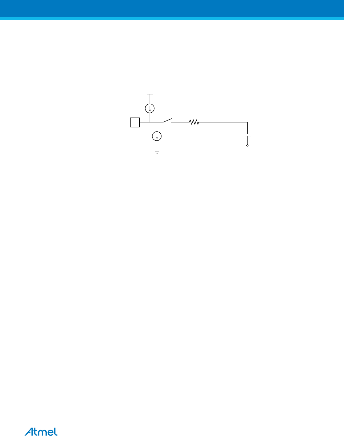
sampling time will depend on how long time the source needs to charge the S/H capacitor, with can vary
widely. The user is recommended to only use low impedance sources with slowly varying signals, since
this minimizes the required charge transfer to the S/H capacitor.
Signal components higher than the Nyquist frequency (fADC/2) should not be present for either kind of
channels, to avoid distortion from unpredictable signal convolution. The user is advised to remove high
frequency components with a low-pass filter before applying the signals as inputs to the ADC.
Figure 27-6 Analog Input Circuitry
ADCn
IIH
1..100k Ω
CS/H
= 14pF
IIL
VCC/2
27.6.2. Analog Noise Canceling Techniques
Digital circuitry inside and outside the device generates EMI which might affect the accuracy of analog
measurements. If conversion accuracy is critical, the noise level can be reduced by applying the following
techniques:
1. Keep analog signal paths as short as possible. Make sure analog tracks run over the analog
ground plane, and keep them well away from high-speed switching digital tracks.
1.1. The AVCC pin on the device should be connected to the digital VCC supply voltage via an LC
network as shown in the figure below.
1.2. Use the ADC noise canceler function to reduce induced noise from the CPU.
1.3. If any ADC [3:0] port pins are used as digital outputs, it is essential that these do not switch
while a conversion is in progress. However, using the 2-wire Interface (ADC4 and ADC5) will only
affect the conversion on ADC4 and ADC5 and not the other ADC channels.
Atmel ATmega8A [DATASHEET]
Atmel-8159F-8-bit AVR Microcontroller_Datasheet_Complete-09/2015
254
Figure 27-7 ADC Power Connections
GND
VCC
PC5 (ADC5/SCL)
PC4 (ADC4/SDA)
PC3 (ADC3)
PC2 (ADC2)
PC1 (ADC1)
PC0 (ADC0)
ADC7
GND
AREF
AVCC
ADC6
PB5
10mH
100nF Analog Ground Plane
27.6.3. ADC Accuracy Definitions
An n-bit single-ended ADC converts a voltage linearly between GND and VREF in 2n steps (LSBs). The
lowest code is read as 0, and the highest code is read as 2n-1.
Several parameters describe the deviation from the ideal behavior:
•Offset: The deviation of the first transition (0x000 to 0x001) compared to the ideal transition (at 0.5
LSB). Ideal value: 0 LSB.
Atmel ATmega8A [DATASHEET]
Atmel-8159F-8-bit AVR Microcontroller_Datasheet_Complete-09/2015
255
Figure 27-8 Offset Error
Output Code
V
REF Input Voltage
Ideal ADC
Actual ADC
Offset
Error
•Gain error: After adjusting for offset, the gain error is found as the deviation of the last transition
(0x3FE to 0x3FF) compared to the ideal transition (at 1.5 LSB below maximum). Ideal value: 0 LSB.
Figure 27-9 Gain Error
Output Code
V
REF Input Voltage
Ideal ADC
Actual ADC
Gain
Error
•Integral Non-linearity (INL): After adjusting for offset and gain error, the INL is the maximum
deviation of an actual transition compared to an ideal transition for any code. Ideal value: 0 LSB.
Figure 27-10 Integral Non-linearity (INL)
Output Code
V
REF Input Voltage
Ideal ADC
Actual ADC
INL
Atmel ATmega8A [DATASHEET]
Atmel-8159F-8-bit AVR Microcontroller_Datasheet_Complete-09/2015
256
•Differential Non-linearity (DNL): The maximum deviation of the actual code width (the interval
between two adjacent transitions) from the ideal code width (1 LSB). Ideal value: 0 LSB.
Figure 27-11 Differential Non-linearity (DNL)
Output Code
0x3FF
0x000
0V
REF Input Voltage
DNL
1 LSB
•Quantization Error: Due to the quantization of the input voltage into a finite number of codes, a
range of input voltages (1 LSB wide) will code to the same value. Always ±0.5 LSB.
•Absolute accuracy: The maximum deviation of an actual (unadjusted) transition compared to an
ideal transition for any code. This is the compound effect of offset, gain error, differential error, non-
linearity, and quantization error. Ideal value: ±0.5 LSB.
27.7. ADC Conversion Result
After the conversion is complete (ADCSRA.ADIF is set), the conversion result can be found in the ADC
Result Registers (ADCL, ADCH).
For single ended conversion, the result is
ADC = IN 1024
REF
where VIN is the voltage on the selected input pin, and VREF the selected voltage reference (see also
descriptions of ADMUX.REFSn and ADMUX.MUX). 0x000 represents analog ground, and 0x3FF
represents the selected reference voltage minus one LSB.
27.8. Register Description
Atmel ATmega8A [DATASHEET]
Atmel-8159F-8-bit AVR Microcontroller_Datasheet_Complete-09/2015
257
27.8.1. ADMUX – ADC Multiplexer Selection Register
When using the I/O specific commands IN and OUT, the I/O addresses 0x00 - 0x3F must be used. When
addressing I/O Registers as data space using LD and ST instructions, 0x20 must be added to these offset
addresses. The device is a complex microcontroller with more peripheral units than can be supported
within the 64 location reserved in Opcode for the IN and OUT instructions. For the Extended I/O space
from 0x60 in SRAM, only the ST/STS/STD and LD/LDS/LDD instructions can be used.
Name: ADMUX
Offset: 0x07
Reset: 0x00
Property:
When addressing I/O Registers as data space the offset address is 0x27
Bit 7 6 5 4 3 2 1 0
REFS1 REFS0 ADLAR MUX3 MUX2 MUX1 MUX0
Access R/W R/W R/W R/W R/W R/W R/W
Reset 0 0 0 0 0 0 0
Bits 7:6 – REFSn: Reference Selection [n = 1:0]
These bits select the voltage reference for the ADC. If these bits are changed during a conversion, the
change will not go in effect until this conversion is complete (ADIF in ADCSRA is set). The internal
voltage reference options may not be used if an external reference voltage is being applied to the AREF
pin.
Table 27-2 ADC Voltage Reference Selection
REFS[1:0] Voltage Reference Selection
00 AREF, Internal Vref turned off
01 AVCC with external capacitor at AREF pin
10 Reserved
11 Internal 2.56V Voltage Reference with external capacitor at AREF pin
Bit 5 – ADLAR: ADC Left Adjust Result
The ADLAR bit affects the presentation of the ADC conversion result in the ADC Data Register. Write one
to ADLAR to left adjust the result. Otherwise, the result is right adjusted. Changing the ADLAR bit will
affect the ADC Data Register immediately, regardless of any ongoing conversions. For a complete
description of this bit, see ADCL and ADCH.
Bits 3:0 – MUXn: Analog Channel Selection [n = 3:0]
The value of these bits selects which analog inputs are connected to the ADC. If these bits are changed
during a conversion, the change will not go in effect until this conversion is complete (ADIF in ADCSRA is
set).
Table 27-3 Input Channel Selection
MUX[3:0] Single Ended Input
0000 ADC0
0001 ADC1
0010 ADC2
Atmel ATmega8A [DATASHEET]
Atmel-8159F-8-bit AVR Microcontroller_Datasheet_Complete-09/2015
258

MUX[3:0] Single Ended Input
0011 ADC3
0100 ADC4
0101 ADC5
0110 ADC6
0111 ADC7
1000 Reserved
1001 Reserved
1010 Reserved
1011 Reserved
1100 Reserved
1101 Reserved
1110 1.30V (VBG)
1111 0V (GND)
Atmel ATmega8A [DATASHEET]
Atmel-8159F-8-bit AVR Microcontroller_Datasheet_Complete-09/2015
259

27.8.2. ADCSRA – ADC Control and Status Register A
When using the I/O specific commands IN and OUT, the I/O addresses 0x00 - 0x3F must be used. When
addressing I/O Registers as data space using LD and ST instructions, 0x20 must be added to these offset
addresses. The device is a complex microcontroller with more peripheral units than can be supported
within the 64 location reserved in Opcode for the IN and OUT instructions. For the Extended I/O space
from 0x60 in SRAM, only the ST/STS/STD and LD/LDS/LDD instructions can be used.
Name: ADCSRA
Offset: 0x06
Reset: 0x00
Property:
When addressing I/O Registers as data space the offset address is 0x26
Bit 7 6 5 4 3 2 1 0
ADEN ADSC ADFR ADIF ADIE ADPS2 ADPS1 ADPS0
Access R/W R/W R/W R/W R/W R/W R/W R/W
Reset 0 0 0 0 0 0 0 0
Bit 7 – ADEN: ADC Enable
Writing this bit to one enables the ADC. By writing it to zero, the ADC is turned off. Turning the ADC off
while a conversion is in progress, will terminate this conversion.
Bit 6 – ADSC: ADC Start Conversion
In Single Conversion mode, write this bit to one to start each conversion. In Free Running mode, write
this bit to one to start the first conversion. The first conversion after ADSC has been written after the ADC
has been enabled, or if ADSC is written at the same time as the ADC is enabled, will take 25 ADC clock
cycles instead of the normal 13. This first conversion performs initialization of the ADC.
ADSC will read as one as long as a conversion is in progress. When the conversion is complete, it returns
to zero. Writing zero to this bit has no effect.
Bit 5 – ADFR: ADC Free Running Select
When this bit is set (one) the ADC operates in Free Running mode. In this mode, the ADC samples and
updates the Data Registers continuously. Clearing this bit (zero) will terminate Free Running mode.
Bit 4 – ADIF: ADC Interrupt Flag
This bit is set when an ADC conversion completes and the Data Registers are updated. The ADC
Conversion Complete Interrupt is executed if the ADIE bit and the I-bit in SREG are set. ADIF is cleared
by hardware when executing the corresponding interrupt Handling Vector. Alternatively, ADIF is cleared
by writing a logical one to the flag. Beware that if doing a Read-Modify-Write on ADCSRA, a pending
interrupt can be disabled. This also applies if the SBI and CBI instructions are used.
Bit 3 – ADIE: ADC Interrupt Enable
When this bit is written to one and the I-bit in SREG is set, the ADC Conversion Complete Interrupt is
activated.
Bits 2:0 – ADPSn: ADC Prescaler Select [n = 2:0]
These bits determine the division factor between the XTAL frequency and the input clock to the ADC.
Atmel ATmega8A [DATASHEET]
Atmel-8159F-8-bit AVR Microcontroller_Datasheet_Complete-09/2015
260

Table 27-4 ADC Prescaler Selections
ADPS[2:0] Division Factor
000 2
001 2
010 4
011 8
100 16
101 32
110 64
111 128
Atmel ATmega8A [DATASHEET]
Atmel-8159F-8-bit AVR Microcontroller_Datasheet_Complete-09/2015
261

27.8.3. ADCL – ADC Data Register Low (ADLAR=0)
When using the I/O specific commands IN and OUT, the I/O addresses 0x00 - 0x3F must be used. When
addressing I/O Registers as data space using LD and ST instructions, 0x20 must be added to these offset
addresses. The device is a complex microcontroller with more peripheral units than can be supported
within the 64 location reserved in Opcode for the IN and OUT instructions. For the Extended I/O space
from 0x60 in SRAM, only the ST/STS/STD and LD/LDS/LDD instructions can be used.
When an ADC conversion is complete, the result is found in these two registers.
When ADCL is read, the ADC Data Register is not updated until ADCH is read. Consequently, if the result
is left adjusted and no more than 8-bit precision is required, it is sufficient to read ADCH. Otherwise,
ADCL must be read first, then ADCH.
The ADLAR bit and the MUXn bits in ADMUX affect the way the result is read from the registers. If
ADLAR is set, the result is left adjusted. If ADLAR is cleared (default), the result is right adjusted.
Name: ADCL
Offset: 0x04
Reset: 0x00
Property:
When addressing I/O Registers as data space the offset address is 0x24
Bit 7 6 5 4 3 2 1 0
ADC7 ADC6 ADC5 ADC4 ADC3 ADC2 ADC1 ADC0
Access R R R R R R R R
Reset 0 0 0 0 0 0 0 0
Bits 7:0 – ADCn: ADC Conversion Result [n = 7:0]
These bits represent the result from the conversion. Refer to ADC Conversion Result on page 257 for
details.
Atmel ATmega8A [DATASHEET]
Atmel-8159F-8-bit AVR Microcontroller_Datasheet_Complete-09/2015
262

27.8.4. ADCH – ADC Data Register High (ADLAR=0)
When using the I/O specific commands IN and OUT, the I/O addresses 0x00 - 0x3F must be used. When
addressing I/O Registers as data space using LD and ST instructions, 0x20 must be added to these offset
addresses. The device is a complex microcontroller with more peripheral units than can be supported
within the 64 location reserved in Opcode for the IN and OUT instructions. For the Extended I/O space
from 0x60 in SRAM, only the ST/STS/STD and LD/LDS/LDD instructions can be used.
Name: ADCH
Offset: 0x05
Reset: 0x00
Property:
When addressing I/O Registers as data space the offset address is 0x25
Bit 7 6 5 4 3 2 1 0
ADC9 ADC8
Access R R
Reset 0 0
Bit 1 – ADC9: ADC Conversion Result
Refer to ADCL.
Bit 0 – ADC8: ADC Conversion Result
Atmel ATmega8A [DATASHEET]
Atmel-8159F-8-bit AVR Microcontroller_Datasheet_Complete-09/2015
263

27.8.5. ADCL – ADC Data Register Low (ADLAR=1)
When using the I/O specific commands IN and OUT, the I/O addresses 0x00 - 0x3F must be used. When
addressing I/O Registers as data space using LD and ST instructions, 0x20 must be added to these offset
addresses. The device is a complex microcontroller with more peripheral units than can be supported
within the 64 location reserved in Opcode for the IN and OUT instructions. For the Extended I/O space
from 0x60 in SRAM, only the ST/STS/STD and LD/LDS/LDD instructions can be used.
Name: ADCL
Offset: 0x04
Reset: 0x00
Property:
When addressing I/O Registers as data space the offset address is 0x24
Bit 7 6 5 4 3 2 1 0
ADC1 ADC0
Access R R
Reset 0 0
Bit 7 – ADC1: ADC Conversion Result
Refer to ADCL.
Bit 6 – ADC0: ADC Conversion Result
Atmel ATmega8A [DATASHEET]
Atmel-8159F-8-bit AVR Microcontroller_Datasheet_Complete-09/2015
264

27.8.6. ADCH – ADC Data Register High (ADLAR=1)
When using the I/O specific commands IN and OUT, the I/O addresses 0x00 - 0x3F must be used. When
addressing I/O Registers as data space using LD and ST instructions, 0x20 must be added to these offset
addresses. The device is a complex microcontroller with more peripheral units than can be supported
within the 64 location reserved in Opcode for the IN and OUT instructions. For the Extended I/O space
from 0x60 in SRAM, only the ST/STS/STD and LD/LDS/LDD instructions can be used.
Name: ADCH
Offset: 0x05
Reset: 0x00
Property:
When addressing I/O Registers as data space the offset address is 0x25
Bit 7 6 5 4 3 2 1 0
ADC7 ADC6 ADC5 ADC4 ADC3 ADC2 ADC1 ADC0
Access R R R R R R R R
Reset 0 0 0 0 0 0 0 0
Bits 7:0 – ADCn: ADC Conversion Result [n = 7:0]
Refer to ADCL.
Atmel ATmega8A [DATASHEET]
Atmel-8159F-8-bit AVR Microcontroller_Datasheet_Complete-09/2015
265

28. Boot Loader Support – Read-While-Write Self-Programming
28.1. Features
•Read-While-Write Self-Programming
•Flexible Boot Memory Size
•High Security (Separate Boot Lock Bits for a Flexible Protection)
•Separate Fuse to Select Reset Vector
•Optimized Page(1) Size
•Code Efficient Algorithm
•Efficient Read-Modify-Write Support
Note: 1. A page is a section in the Flash consisting of several bytes (see Table. No. of Words in a Page
and No. of Pages in the Flash in Page Size) used during programming. The page organization does not
affect normal operation.
Related Links
Page Size on page 286
28.2. Overview
In this device, the Boot Loader Support provides a real Read-While-Write Self-Programming mechanism
for downloading and uploading program code by the MCU itself. This feature allows flexible application
software updates controlled by the MCU using a Flash-resident Boot Loader program. The Boot Loader
program can use any available data interface and associated protocol to read code and write (program)
that code into the Flash memory, or read the code from the program memory. The program code within
the Boot Loader section has the capability to write into the entire Flash, including the Boot Loader
memory. The Boot Loader can thus even modify itself, and it can also erase itself from the code if the
feature is not needed anymore. The size of the Boot Loader memory is configurable with fuses and the
Boot Loader has two separate sets of Boot Lock bits which can be set independently. This gives the user
a unique flexibility to select different levels of protection.
28.3. Application and Boot Loader Flash Sections
The Flash memory is organized in two main sections, the Application section and the Boot Loader
section. The size of the different sections is configured by the BOOTSZ Fuses. These two sections can
have different level of protection since they have different sets of Lock bits.
28.3.1. Application Section
The Application section is the section of the Flash that is used for storing the application code. The
protection level for the Application section can be selected by the application Boot Lock bits (Boot Lock
bits 0). The Application section can never store any Boot Loader code since the SPM instruction is
disabled when executed from the Application section.
28.3.2. BLS – Boot Loader Section
While the Application section is used for storing the application code, the The Boot Loader software must
be located in the BLS since the SPM instruction can initiate a programming when executing from the BLS
only. The SPM instruction can access the entire Flash, including the BLS itself. The protection level for
the Boot Loader section can be selected by the Boot Loader Lock bits (Boot Lock bits 1).
Atmel ATmega8A [DATASHEET]
Atmel-8159F-8-bit AVR Microcontroller_Datasheet_Complete-09/2015
266

28.4. Read-While-Write and No Read-While-Write Flash Sections
Whether the CPU supports Read-While-Write or if the CPU is halted during a Boot Loader software
update is dependent on which address that is being programmed. In addition to the two sections that are
configurable by the BOOTSZ Fuses as described above, the Flash is also divided into two fixed sections,
the Read-While-Write (RWW) section and the No Read-While-Write (NRWW) section. The limit between
the RWW- and NRWW sections is given in the Boot Loader Parameters section and Figure 28-2 Memory
Sections on page 269. The main difference between the two sections is:
•When erasing or writing a page located inside the RWW section, the NRWW section can be read
during the operation
•When erasing or writing a page located inside the NRWW section, the CPU is halted during the
entire operation
The user software can never read any code that is located inside the RWW section during a Boot Loader
software operation. The syntax “Read-While-Write section” refers to which section that is being
programmed (erased or written), not which section that actually is being read during a Boot Loader
software update.
Related Links
ATmega8A Boot Loader Parameters on page 278
28.4.1. RWW – Read-While-Write Section
If a Boot Loader software update is programming a page inside the RWW section, it is possible to read
code from the Flash, but only code that is located in the NRWW section. During an on-going
programming, the software must ensure that the RWW section never is being read. If the user software is
trying to read code that is located inside the RWW section (i.e. by a call/rjmp/lpm or an interrupt) during
programming, the software might end up in an unknown state. To avoid this, the interrupts should either
be disabled or moved to the Boot Loader section. The Boot Loader section is always located in the
NRWW section. The RWW Section Busy bit (RWWSB) in the Store Program Memory Control Register
(SPMCR) will be read as logical one as long as the RWW section is blocked for reading. After a
programming is completed, the RWWSB must be cleared by software before reading code located in the
RWW section. Please refer to SPMCR – Store Program Memory Control Register in this chapter for
details on how to clear RWWSB.
28.4.2. NRWW – No Read-While-Write Section
The code located in the NRWW section can be read when the Boot Loader software is updating a page in
the RWW section. When the Boot Loader code updates the NRWW section, the CPU is halted during the
entire Page Erase or Page Write operation.
Table 28-1 Read-While-Write Features
Which Section does the Z-
pointer Address during the
Programming?
Which Section can be read
during Programming?
CPU Halted? Read-While-Write
Supported?
RWW Section NRWW Section No Yes
NRWW Section None Yes No
Atmel ATmega8A [DATASHEET]
Atmel-8159F-8-bit AVR Microcontroller_Datasheet_Complete-09/2015
267
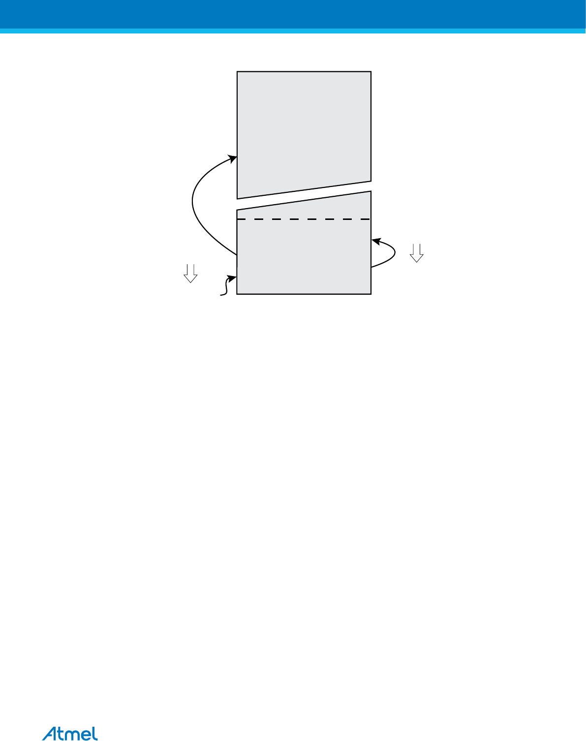
Figure 28-1 Read-While-Write vs. No Read-While-Write
Read-While-Write
(RWW) Section
No Read-While-Write
(NRWW) Section
Z-pointer
Addresses RWW
Section
Z-pointer
Addresses NRWW
Section
CPU is Halted
During the Operation
Code Located in
NRWW Section
Can be Read During
the Operation
Atmel ATmega8A [DATASHEET]
Atmel-8159F-8-bit AVR Microcontroller_Datasheet_Complete-09/2015
268
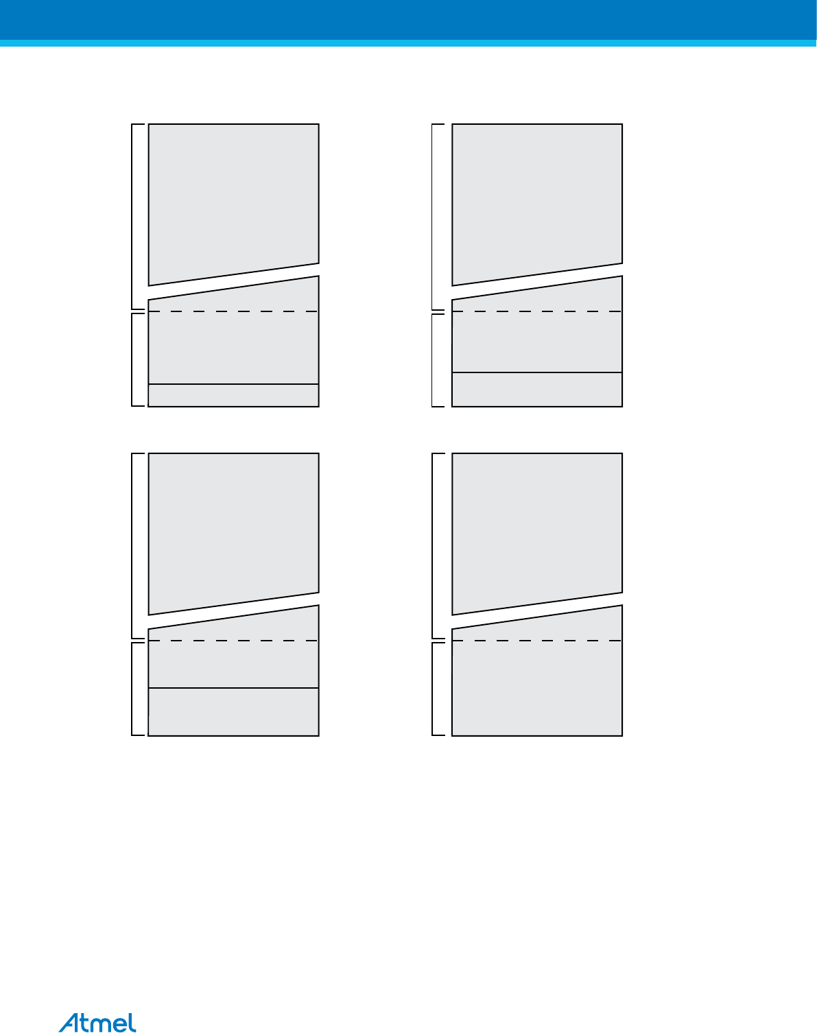
Figure 28-2 Memory Sections
0x0000
Flashend
Program Memory
BOOTSZ = '11'
Application Flash Section
Boot Loader Flash Section
Flashend
Program Memory
BOOTSZ = '10'
0x0000
Program Memory
BOOTSZ = '01'
Program Memory
BOOTSZ = '00'
Application Flash Section
Boot Loader Flash Section
0x0000
Flashend
Application Flash Section
Flashend
End RWW
Start NRWW
Application Flash Section
Boot Loader Flash Section
Boot Loader Flash Section
End RWW
Start NRWW
End RWW
Start NRWW
0x0000
End RWW, End Application
Start NRWW, Start Boot Loader
Application Flash SectionApplication Flash Section
Application Flash Section
Read-While-Write SectionNo Read-While-Write Section Read-While-Write SectionNo Read-While-Write Section
Read-While-Write SectionNo Read-While-Write SectionRead-While-Write SectionNo Read-While-Write Section
End Application
Start Boot Loader
End Application
Start Boot Loader
End Application
Start Boot Loader
Related Links
ATmega8A Boot Loader Parameters on page 278
28.5. Boot Loader Lock Bits
If no Boot Loader capability is needed, the entire Flash is available for application code. The Boot Loader
has two separate sets of Boot Lock bits which can be set independently. This gives the user a unique
flexibility to select different levels of protection.
The user can select:
•To protect the entire Flash from a software update by the MCU
•To protect only the Boot Loader Flash section from a software update by the MCU
Atmel ATmega8A [DATASHEET]
Atmel-8159F-8-bit AVR Microcontroller_Datasheet_Complete-09/2015
269

•To protect only the Application Flash section from a software update by the MCU
•Allow software update in the entire Flash
The Boot Lock bits can be set in software and in Serial or Parallel Programming mode, but they can be
cleared by a Chip Erase command only. The general Write Lock (Lock Bit mode 2) does not control the
programming of the Flash memory by SPM instruction. Similarly, the general Read/Write Lock (Lock Bit
mode 1) does not control reading nor writing by LPM/SPM, if it is attempted.
Table 28-2 Boot Lock Bit0 Protection Modes (Application Section)
BLB0
Mode
BLB02 BLB01 Protection
1 1 1 No restrictions for SPM or LPM accessing the Application section.
2 1 0 SPM is not allowed to write to the Application section.
3 0 0 SPM is not allowed to write to the Application section, and LPM executing
from the Boot Loader section is not allowed to read from the Application
section. If Interrupt Vectors are placed in the Boot Loader section,
interrupts are disabled while executing from the Application section.
4 0 1 LPM executing from the Boot Loader section is not allowed to read from
the Application section. If Interrupt Vectors are placed in the Boot Loader
section, interrupts are disabled while executing from the Application
section.
Note: “1” means unprogrammed, “0” means programmed.
Table 28-3 Boot Lock Bit1 Protection Modes (Boot Loader Section)
BLB1
Mode
BLB12 BLB11 Protection
1 1 1 No restrictions for SPM or LPM accessing the Boot Loader section.
2 1 0 SPM is not allowed to write to the Boot Loader section.
3 0 0 SPM is not allowed to write to the Boot Loader section, and LPM executing
from the Application section is not allowed to read from the Boot Loader
section. If Interrupt Vectors are placed in the Application section, interrupts
are disabled while executing from the Boot Loader section.
4 0 1 LPM executing from the Application section is not allowed to read from the
Boot Loader section. If Interrupt Vectors are placed in the Application
section, interrupts are disabled while executing from the Boot Loader
section.
Note: “1” means unprogrammed, “0” means programmed.
28.6. Entering the Boot Loader Program
Entering the Boot Loader takes place by a jump or call from the application program. This may be initiated
by a trigger such as a command received via USART, or SPI interface. Alternatively, the Boot Reset Fuse
can be programmed so that the Reset Vector is pointing to the Boot Flash start address after a reset. In
this case, the Boot Loader is started after a reset. After the application code is loaded, the program can
start executing the application code. The fuses cannot be changed by the MCU itself. This means that
Atmel ATmega8A [DATASHEET]
Atmel-8159F-8-bit AVR Microcontroller_Datasheet_Complete-09/2015
270
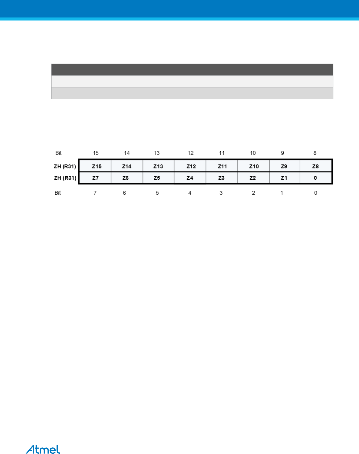
once the Boot Reset Fuse is programmed, the Reset Vector will always point to the Boot Loader Reset
and the fuse can only be changed through the serial or parallel programming interface.
Table 28-4 Boot Reset Fuse
BOOTRST Reset Address
1 Reset Vector = Application Reset (address 0x0000)
0 Reset Vector = Boot Loader Reset (see Table Boot Size Configuration)
Note: “1” means unprogrammed, “0” means programmed.
28.7. Addressing the Flash During Self-Programming
The Z-pointer is used to address the SPM commands.
Since the Flash is organized in pages, the Program Counter can be treated as having two different
sections. One section, consisting of the least significant bits, is addressing the words within a page, while
the most significant bits are addressing the pages. This is shown in the following figure. The Page Erase
and Page Write operations are addressed independently. Therefore it is of major importance that the Boot
Loader software addresses the same page in both the Page Erase and Page Write operation. Once a
programming operation is initiated, the address is latched and the Z-pointer can be used for other
operations.
The only SPM operation that does not use the Z-pointer is Setting the Boot Loader Lock bits. The content
of the Z-pointer is ignored and will have no effect on the operation. The LPM instruction does also use the
Z-pointer to store the address. Since this instruction addresses the Flash byte-by-byte, also the LSB (bit
Z0) of the Z-pointer is used.
Atmel ATmega8A [DATASHEET]
Atmel-8159F-8-bit AVR Microcontroller_Datasheet_Complete-09/2015
271
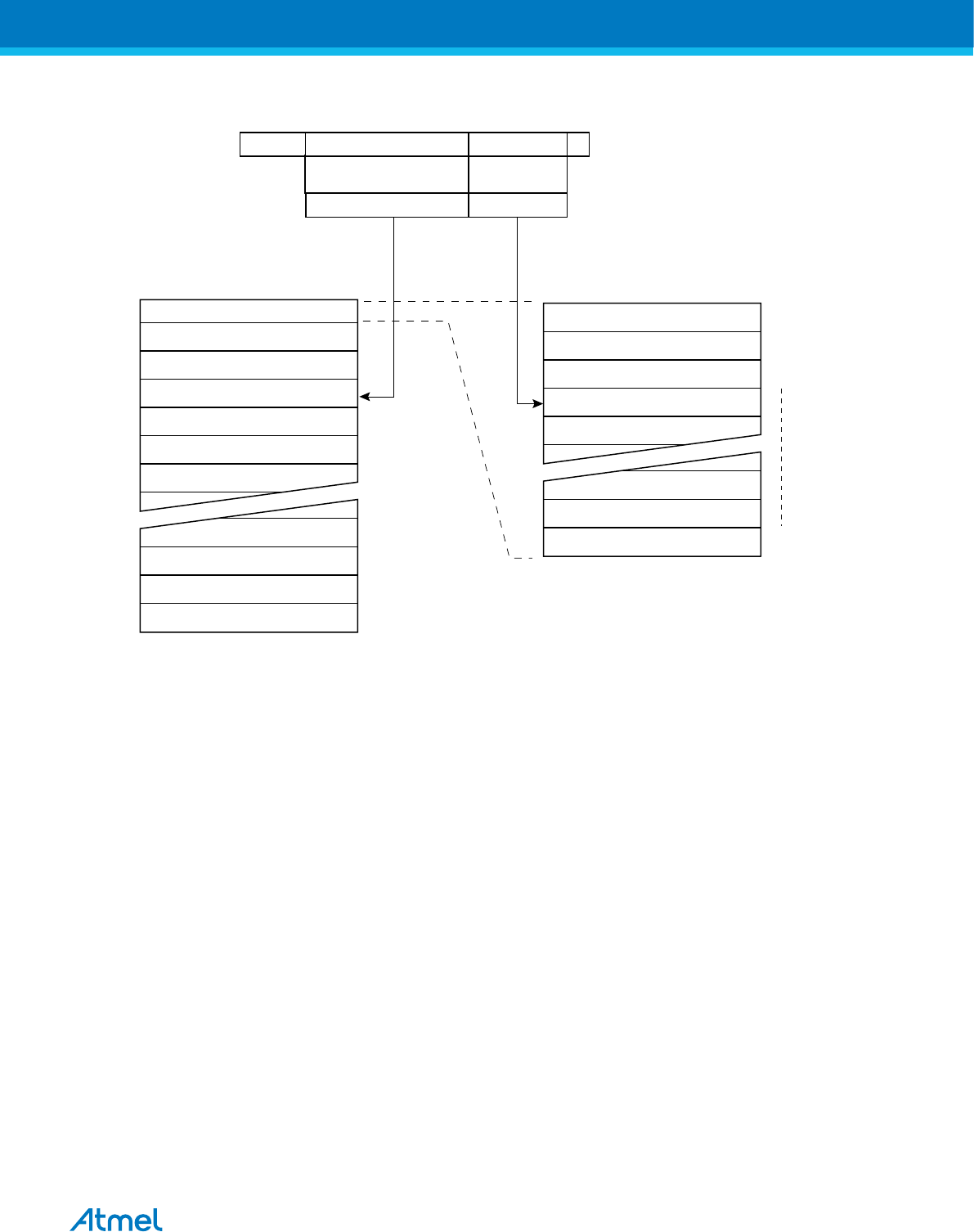
Figure 28-3 Addressing the Flash During SPM(1)
PROGRAM MEMORY
0115
Z - REGISTER
BIT
0
ZPAGEMSB
WORD ADDRESS
WITHIN A PAGE
PAGE ADDRESS
WITHIN THE FLASH
ZPCMSB
INSTRUCTION WORD
PAGE PCWORD[PAGEMSB:0]:
00
01
02
PAGEEND
PAGE
PCWORDPCPAGE
PCMSB PAGEMSB
PROGRAM
COUNTER
Note:
1. The different variables used in the figure are listed in Table 28-8 Explanation of Different Variables
used in Figure and the Mapping to the Z-pointer, ATmega8A on page 279.
2. PCPAGE and PCWORD are listed in table Number of Words in a Page and number of Pages in the
Flash in the Signal Names section.
28.8. Self-Programming the Flash
The program memory is updated in a page by page fashion. Before programming a page with the data
stored in the temporary page buffer, the page must be erased. The temporary page buffer is filled one
word at a time using SPM and the buffer can be filled either before the Page Erase command or between
a Page Erase and a Page Write operation:
Alternative 1, fill the buffer before a Page Erase
•Fill temporary page buffer
•Perform a Page Erase
•Perform a Page Write
Alternative 2, fill the buffer after Page Erase
•Perform a Page Erase
•Fill temporary page buffer
•Perform a Page Write
Atmel ATmega8A [DATASHEET]
Atmel-8159F-8-bit AVR Microcontroller_Datasheet_Complete-09/2015
272

If only a part of the page needs to be changed, the rest of the page must be stored (for example in the
temporary page buffer) before the erase, and then be rewritten. When using alternative 1, the Boot
Loader provides an effective Read-Modify-Write feature which allows the user software to first read the
page, do the necessary changes, and then write back the modified data. If alternative 2 is used, it is not
possible to read the old data while loading since the page is already erased. The temporary page buffer
can be accessed in a random sequence. It is essential that the page address used in both the Page
Erase and Page Write operation is addressing the same page. Please refer to Simple Assembly Code
Example for a Boot Loader for an assembly code example.
28.8.1. Performing Page Erase by SPM
To execute page erase, set up the address in the Z-pointer, write “X0000011” to SPMCR and execute
SPM within four clock cycles after writing SPMCR. The data in R1 and R0 is ignored. The page address
must be written to PCPAGE in the Z-register. Other bits in the Z-pointer will be ignored during this
operation.
•Page Erase to the RWW section: The NRWW section can be read during the Page Erase.
•Page Erase to the NRWW section: The CPU is halted during the operation.
Note: If an interrupt occurs in the timed sequence the four cycle access cannot be guaranteed. In order
to ensure atomic operation disable interrupts before writing to SPMCR.
28.8.2. Filling the Temporary Buffer (Page Loading)
To write an instruction word, set up the address in the Z-pointer and data in R1:R0, write “00000001” to
SPMCR and execute SPM within four clock cycles after writing SPMCR. The content of PCWORD in the
Z-register is used to address the data in the temporary page buffer. The temporary buffer will auto-erase
after a page write operation or by writing the RWWSRE bit in SPMCR. It is also erased after a System
Reset. Note that it is not possible to write more than one time to each address without erasing the
temporary buffer.
Note: If the EEPROM is written in the middle of an SPM Page Load operation, all data loaded will be
lost.
28.8.3. Performing a Page Write
To execute page write, set up the address in the Z-pointer, write “X0000101” to SPMCR and execute
SPM within four clock cycles after writing SPMCR. The data in R1 and R0 is ignored. The page address
must be written to PCPAGE. Other bits in the Z-pointer must be written to zero during this operation.
•Page Write to the RWW section: The NRWW section can be read during the Page Write
•Page Write to the NRWW section: The CPU is halted during the operation
Note: If an interrupt occurs in the timed sequence the four cycle access cannot be guaranteed. In order
to ensure atomic operation disable interrupts before writing to SPMCSR.
28.8.4. Using the SPM Interrupt
If the SPM interrupt is enabled, the SPM interrupt will generate a constant interrupt when the SPMEN bit
in SPMCR is cleared. This means that the interrupt can be used instead of polling the SPMCR Register in
software. When using the SPM interrupt, the Interrupt Vectors should be moved to the BLS section to
avoid that an interrupt is accessing the RWW section when it is blocked for reading. How to move the
interrupts is described in Interrupts chapter.
Related Links
Interrupts on page 66
Atmel ATmega8A [DATASHEET]
Atmel-8159F-8-bit AVR Microcontroller_Datasheet_Complete-09/2015
273

28.8.5. Consideration While Updating Boot Loader Section (BLS)
Special care must be taken if the user allows the Boot Loader Section (BLS) to be updated by leaving
Boot Lock bit11 unprogrammed. An accidental write to the Boot Loader itself can corrupt the entire Boot
Loader, and further software updates might be impossible. If it is not necessary to change the Boot
Loader software itself, it is recommended to program the Boot Lock bit11 to protect the Boot Loader
software from any internal software changes.
28.8.6. Prevent Reading the RWW Section During Self-Programming
During Self-Programming (either page erase or page write), the RWW section is always blocked for
reading. The user software itself must prevent that this section is addressed during the self programming
operation. The RWWSB in the SPMCR will be set as long as the RWW section is busy. During Self-
Programming the Interrupt Vector table should be moved to the BLS as described in Interrupts, or the
interrupts must be disabled. Before addressing the RWW section after the programming is completed, the
user software must clear the RWWSB by writing the RWWSRE. Please refer to Simple Assembly Code
Example for a Boot Loader for an example.
Related Links
Interrupts on page 66
28.8.7. Setting the Boot Loader Lock Bits by SPM
To set the Boot Loader Lock Bits, write the desired data to R0, write “X0001001” to SPMCR and execute
SPM within four clock cycles after writing SPMCR. The only accessible Lock Bits are the Boot Lock Bits
that may prevent the Application and Boot Loader section from any software update by the MCU.
Bit 7 6 5 4 3 2 1 0
Rd – – – – – – LB2 LB1
BLB01
BLB02
BLB11
BLB12
1
1 1 1
The tables in Boot Loader Lock Bits on page 269 show how the different settings of the Boot Loader bits
affect the Flash access.
If bits 5:2 in R0 are cleared (zero), the corresponding Boot Lock bit will be programmed if an SPM
instruction is executed within four cycles after BLBSET and SPMEN are set in SPMCR. The Z-pointer is
don’t care during this operation, but for future compatibility it is recommended to load the Z-pointer with
0x0001 (same as used for reading the Lock Bits). For future compatibility It is also recommended to set
bits 7, 6, 1, and 0 in R0 to “1” when writing the Lock Bits. When programming the Lock Bits the entire
Flash can be read during the operation.
28.8.8. EEPROM Write Prevents Writing to SPMCR
Note that an EEPROM write operation will block all software programming to Flash. Reading the Fuses
and Lock Bits from software will also be prevented during the EEPROM write operation. It is
recommended that the user checks the status bit (EEWE) in the EECR Register and verifies that the bit is
cleared before writing to the SPMCR Register.
28.8.9. Reading the Fuse and Lock Bits from Software
It is possible to read both the Fuse and Lock Bits from software. To read the Lock Bits, load the Z-pointer
with 0x0001 and set the BLBSET and SPMEN bits in SPMCR. When an LPM instruction is executed
within three CPU cycles after the BLBSET and SPMEN bits are set in SPMCR, the value of the Lock Bits
will be loaded in the destination register. The BLBSET and SPMEN bits will auto-clear upon completion of
reading the Lock Bits or if no LPM instruction is executed within three CPU cycles or no SPM instruction
is executed within four CPU cycles. When BLBSET and SPMEN are cleared, LPM will work as described
in the Instruction set Manual.
Bit 7 6 5 4 3 2 1 0
Rd – – – – – – LB2 LB1
BLB01
BLB02
BLB11
BLB12
–
– LB2 LB1
Atmel ATmega8A [DATASHEET]
Atmel-8159F-8-bit AVR Microcontroller_Datasheet_Complete-09/2015
274
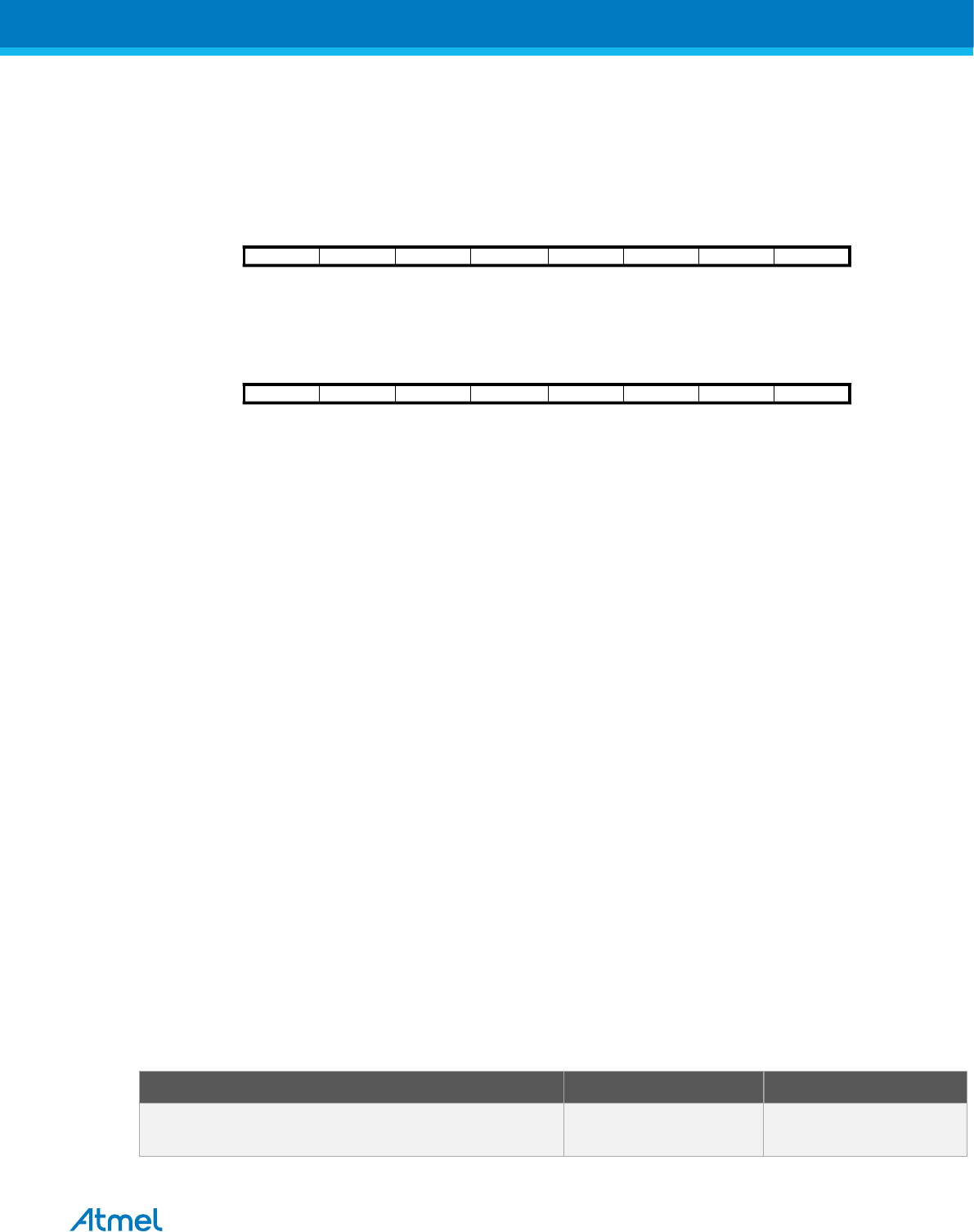
The algorithm for reading the Fuse Low bits is similar to the one described above for reading the Lock
Bits. To read the Fuse Low bits, load the Z-pointer with 0x0000 and set the BLBSET and SPMEN bits in
SPMCR. When an LPM instruction is executed within three cycles after the BLBSET and SPMEN bits are
set in the SPMCR, the value of the Fuse Low bits (FLB) will be loaded in the destination register as
shown below. Refer to Table 25-5 in section Fuse Bits for a detailed description and mapping of the fuse
low bits.
Bit 7 6 5 4 3 2 1 0
Rd FLB7 FLB6 FLB5 FLB4 FLB3 FLB2 FLB1 FLB0
Similarly, when reading the Fuse High bits, load 0x0003 in the Z-pointer. When an LPM instruction is
executed within three cycles after the BLBSET and SPMEN bits are set in the SPMCR, the value of the
Fuse High bits (FHB) will be loaded in the destination register as shown below. Refer to Table 25-3 in
section Fuse Bits for detailed description and mapping of the fuse high bits.
Bit 7 6 5 4 3 2 1 0
Rd FHB7 FHB6 FHB5 FHB4 FHB3 FHB2 FHB1 FHB0
Fuse and Lock bits that are programmed read as '0'. Fuse and Lock bits that are unprogrammed, will read
as '1'.
Related Links
Fuse Bits on page 284
28.8.10. Preventing Flash Corruption
During periods of low VCC, the Flash program can be corrupted because the supply voltage is too low for
the CPU and the Flash to operate properly. These issues are the same as for board level systems using
the Flash, and the same design solutions should be applied.
A Flash program corruption can be caused by two situations when the voltage is too low. First, a regular
write sequence to the Flash requires a minimum voltage to operate correctly. Secondly, the CPU itself can
execute instructions incorrectly, if the supply voltage for executing instructions is too low.
Flash corruption can easily be avoided by following these design recommendations (one is sufficient):
1. If there is no need for a Boot Loader update in the system, program the Boot Loader Lock bits to
prevent any Boot Loader software updates.
2. Keep the AVR RESET active (low) during periods of insufficient power supply voltage. This can be
done by enabling the internal Brown-out Detector (BOD) if the operating voltage matches the
detection level. If not, an external low VCC reset protection circuit can be used. If a reset occurs
while a write operation is in progress, the write operation will be completed provided that the power
supply voltage is sufficient.
3. Keep the AVR core in Power-down sleep mode during periods of low VCC. This will prevent the
CPU from attempting to decode and execute instructions, effectively protecting the SPMCR
Register and thus the Flash from unintentional writes.
28.8.11. Programming Time for Flash when Using SPM
The calibrated RC Oscillator is used to time Flash accesses. The following table shows the typical
programming time for Flash accesses from the CPU.
Table 28-5 SPM Programming Time(1)
Symbol Min. Programming Time Max. Programming Time
Flash write (Page Erase, Page Write, and write Lock bits
by SPM)
3.7ms 4.5ms
Atmel ATmega8A [DATASHEET]
Atmel-8159F-8-bit AVR Microcontroller_Datasheet_Complete-09/2015
275

Note: 1. Minimum and maximum programming time is per individual operation.
28.8.12. Simple Assembly Code Example for a Boot Loader
;-the routine writes one page of data from RAM to Flash
; the first data location in RAM is pointed to by the Y pointer
; the first data location in Flash is pointed to by the Z-pointer
;-error handling is not included
;-the routine must be placed inside the boot space
; (at least the Do_spm sub routine). Only code inside NRWW section can
; be read during self-programming (page erase and page write).
;-registers used: r0, r1, temp1 (r16), temp2 (r17), looplo (r24),
; loophi (r25), spmcrval (r20)
; storing and restoring of registers is not included in the routine
; register usage can be optimized at the expense of code size
;-It is assumed that either the interrupt table is moved to the Boot
; loader section or that the interrupts are disabled.
.equ PAGESIZEB = PAGESIZE*2 ;PAGESIZEB is page size in BYTES, not words
.org SMALLBOOTSTART
Write_page:
; Page Erase
ldi spmcrval, (1<<PGERS) | (1<<SPMEN)
rcall Do_spm
; re-enable the RWW section
ldi spmcrval, (1<<RWWSRE) | (1<<SPMEN)
rcall Do_spm
; transfer data from RAM to Flash page buffer
ldi looplo, low(PAGESIZEB) ;init loop variable
ldi loophi, high(PAGESIZEB) ;not required for PAGESIZEB<=256
Wrloop:
ld r0, Y+
ld r1, Y+
ldi spmcrval, (1<<SPMEN)
rcall Do_spm
adiw ZH:ZL, 2
sbiw loophi:looplo, 2 ;use subi for PAGESIZEB<=256
brne Wrloop
Atmel ATmega8A [DATASHEET]
Atmel-8159F-8-bit AVR Microcontroller_Datasheet_Complete-09/2015
276

; execute Page Write
subi ZL, low(PAGESIZEB) ;restore pointer
sbci ZH, high(PAGESIZEB) ;not required for PAGESIZEB<=256
ldi spmcrval, (1<<PGWRT) | (1<<SPMEN)
rcall Do_spm
; re-enable the RWW section
ldi spmcrval, (1<<RWWSRE) | (1<<SPMEN)
rcall Do_spm
; read back and check, optional
ldi looplo, low(PAGESIZEB) ;init loop variable
ldi loophi, high(PAGESIZEB) ;not required for PAGESIZEB<=256
subi YL, low(PAGESIZEB) ;restore pointer
sbci YH, high(PAGESIZEB)
Rdloop:
lpm r0, Z+
ld r1, Y+
cpse r0, r1
rjmp Error
sbiw loophi:looplo, 1 ;use subi for PAGESIZEB<=256
brne Rdloop
; return to RWW section
; verify that RWW section is safe to read
Return:
in temp1, SPMCR
sbrs temp1, RWWSB ; If RWWSB is set, the RWW section is not ready yet
ret
; re-enable the RWW section
Atmel ATmega8A [DATASHEET]
Atmel-8159F-8-bit AVR Microcontroller_Datasheet_Complete-09/2015
277

ldi spmcrval, (1<<RWWSRE) | (1<<SPMEN)
rcall Do_spm
rjmp Return
Do_spm:
; check for previous SPM complete
Wait_spm:
in temp1, SPMCR
sbrc temp1, SPMEN
rjmp Wait_spm
; input: spmcrval determines SPM action
; disable interrupts if enabled, store status
in temp2, SREG
cli
; check that no EEPROM write access is present
Wait_ee:
sbic EECR, EEWE
rjmp Wait_ee
; SPM timed sequence
out SPMCR, spmcrval
spm
; restore SREG (to enable interrupts if originally enabled)
out SREG, temp2
ret
28.8.13. ATmega8A Boot Loader Parameters
In the following tables, the parameters used in the description of the self programming are given.
Atmel ATmega8A [DATASHEET]
Atmel-8159F-8-bit AVR Microcontroller_Datasheet_Complete-09/2015
278

Table 28-6 Boot Size Configuration, ATmega8A
BOOTSZ1 BOOTSZ0 Boot
Size
Pages Application
Flash Section
Boot
Loader
Flash
Section
End
Application
Section
Boot Reset
Address
(Start Boot
Loader
Section)
1 1 128
words
4 0x000 - 0xF7F 0xF80 -
0xFFF
0xF7F 0xF80
1 0 256
words
8 0x000 - 0xEFF 0xF00 -
0xFFF
0xEFF 0xF00
0 1 512
words
16 0x000 - 0xDFF 0xE00 -
0xFFF
0xDFF 0xE00
0 0 1024
words
32 0x000 - 0xBFF 0xC00 -
0xFFF
0xBFF 0xC00
Note: The different BOOTSZ Fuse configurations are shown in Figure 28-2 Memory Sections on page
269.
Table 28-7 Read-While-Write Limit, ATmega8A
Section Pages Address
Read-While-Write section (RWW) 96 0x000 - 0xBFF
No Read-While-Write section (NRWW) 32 0xC00 - 0xFFF
Note: For details about these two section, see NRWW – No Read-While-Write Section on page 267 and
RWW – Read-While-Write Section.
Table 28-8 Explanation of Different Variables used in Figure and the Mapping to the Z-pointer, ATmega8A
Variable Corresponding Z-
value(1)
Description
PCMSB 11 Most significant bit in the Program Counter. (The Program
Counter is 12 bits PC[11:0])
PAGEMSB 4 Most significant bit which is used to address the words
within one page (32 words in a page requires 5 bits PC
[4:0]).
ZPCMSB Z12 Bit in Z-register that is mapped to PCMSB. Because Z0 is
not used, the ZPCMSB equals PCMSB + 1.
ZPAGEMSB Z5 Bit in Z-register that is mapped to PAGEMSB. Because
Z0 is not used, the ZPAGEMSB equals PAGEMSB + 1.
PCPAGE PC[11:5] Z12:Z6 Program counter page address: Page select, for page
erase and page write
PCWORD PC[4:0] Z5:Z1 Program counter word address: Word select, for filling
temporary buffer (must be zero during page write
operation)
Atmel ATmega8A [DATASHEET]
Atmel-8159F-8-bit AVR Microcontroller_Datasheet_Complete-09/2015
279

Note: 1.
Z15:Z13: always ignored.
Z0: should be zero for all SPM commands, byte select for the LPM instruction.
See Addressing the Flash During Self-Programming for details about the use of Z-pointer during Self-
Programming.
28.9. Register Description
Atmel ATmega8A [DATASHEET]
Atmel-8159F-8-bit AVR Microcontroller_Datasheet_Complete-09/2015
280

28.9.1. SPMCR – Store Program Memory Control Register
The Store Program Memory Control and Status Register contains the control bits needed to control the
Boot Loader operations.
When using the I/O specific commands IN and OUT, the I/O addresses 0x00 - 0x3F must be used. When
addressing I/O Registers as data space using LD and ST instructions, 0x20 must be added to these offset
addresses. The device is a complex microcontroller with more peripheral units than can be supported
within the 64 location reserved in Opcode for the IN and OUT instructions. For the Extended I/O space
from 0x60 in SRAM, only the ST/STS/STD and LD/LDS/LDD instructions can be used.
Name: SPMCR
Offset: 0x37
Reset: 0x00
Property:
When addressing I/O Registers as data space the offset address is 0x57
Bit 7 6 5 4 3 2 1 0
SPMIE RWWSB RWWSRE BLBSET PGWRT PGERS SPMEN
Access R/W R R/W R/W R/W R/W R/W
Reset 0 0 0 0 0 0 0
Bit 7 – SPMIE: SPM Interrupt Enable
When the SPMIE bit is written to one, and the I-bit in the Status Register is set (one), the SPM ready
interrupt will be enabled. The SPM ready Interrupt will be executed as long as the SPMEN bit in the
SPMCR Register is cleared.
Bit 6 – RWWSB: Read-While-Write Section Busy
When a Self-Programming (page erase or page write) operation to the RWW section is initiated, the
RWWSB will be set (one) by hardware. When the RWWSB bit is set, the RWW section cannot be
accessed. The RWWSB bit will be cleared if the RWWSRE bit is written to one after a Self-Programming
operation is completed. Alternatively the RWWSB bit will automatically be cleared if a page load operation
is initiated.
Bit 4 – RWWSRE: Read-While-Write Section Read Enable
When programming (Page Erase or Page Write) to the RWW section, the RWW section is blocked for
reading (the RWWSB will be set by hardware). To re-enable the RWW section, the user software must
wait until the programming is completed (SPMEN will be cleared). Then, if the RWWSRE bit is written to
one at the same time as SPMEN, the next SPM instruction within four clock cycles re-enables the RWW
section. The RWW section cannot be re-enabled while the Flash is busy with a Page Erase or a Page
Write (SPMEN is set). If the RWWSRE bit is written while the Flash is being loaded, the Flash load
operation will abort and the data loaded will be lost.
Bit 3 – BLBSET: Boot Lock Bit Set
If this bit is written to one at the same time as SPMEN, the next SPM instruction within four clock cycles
sets Boot Lock bits, according to the data in R0. The data in R1 and the address in the Z-pointer are
ignored. The BLBSET bit will automatically be cleared upon completion of the Lock bit set, or if no SPM
instruction is executed within four clock cycles.
An LPM instruction within three cycles after BLBSET and SPMEN are set in the SPMCR Register
(SPMCR.BLBSET and SPMCR.SPMEN), will read either the Lock bits or the Fuse bits (depending on Z0
in the Z-pointer) into the destination register. Refer to Reading the Fuse and Lock Bits from Software.
Atmel ATmega8A [DATASHEET]
Atmel-8159F-8-bit AVR Microcontroller_Datasheet_Complete-09/2015
281

Bit 2 – PGWRT: Page Write
If this bit is written to one at the same time as SPMEN, the next SPM instruction within four clock cycles
executes Page Write, with the data stored in the temporary buffer. The page address is taken from the
high part of the Zpointer. The data in R1 and R0 are ignored. The PGWRT bit will auto-clear upon
completion of a Page Write, or if no SPM instruction is executed within four clock cycles. The CPU is
halted during the entire Page Write operation if the NRWW section is addressed.
Bit 1 – PGERS: Page Erase
If this bit is written to one at the same time as SPMEN, the next SPM instruction within four clock cycles
executes Page Erase. The page address is taken from the high part of the Z-pointer. The data in R1 and
R0 are ignored. The PGERS bit will auto-clear upon completion of a Page Erase, or if no SPM instruction
is executed within four clock cycles. The CPU is halted during the entire Page Write operation if the
NRWW section is addressed.
Bit 0 – SPMEN: Store Program Memory
This bit enables the SPM instruction for the next four clock cycles. If written to one together with either
RWWSRE, BLBSET, PGWRT or PGERS, the following SPM instruction will have a special meaning, see
description above. If only SPMEN is written, the following SPM instruction will store the value in R1:R0 in
the temporary page buffer addressed by the Z-pointer. The LSB of the Z-pointer is ignored. The SPMEN
bit will auto-clear upon completion of an SPM instruction, or if no SPM instruction is executed within four
clock cycles. During Page Erase and Page Write, the SPMEN bit remains high until the operation is
completed.
Writing any other combination than “10001”, “01001”, “00101”, “00011” or “00001” in the lower five bits will
have no effect.
Atmel ATmega8A [DATASHEET]
Atmel-8159F-8-bit AVR Microcontroller_Datasheet_Complete-09/2015
282

29. Memory Programming
29.1. Program and Data Memory Lock Bits
The ATmega8A provides six Lock bits. These can be left unprogrammed ('1') or can be programmed ('0')
to obtain the additional features listed in the Lock Bit Protection Modes table below. The Lock Bits can
only be erased to “1” with the Chip Erase command.
Table 29-1 Lock Bit Byte
Lock Bit Byte Bit No. Description Default Value(1)
7 – 1 (unprogrammed)
6 – 1 (unprogrammed)
BLB12 5 Boot Lock bit 1 (unprogrammed)
BLB11 4 Boot Lock bit 1 (unprogrammed)
BLB02 3 Boot Lock bit 1 (unprogrammed)
BLB01 2 Boot Lock bit 1 (unprogrammed)
LB2 1 Lock bit 1 (unprogrammed)
LB1 0 Lock bit 1 (unprogrammed)
Note: 1. “1” means unprogrammed, “0” means programmed.
Table 29-2 Lock Bit Protection Modes(2)
Memory Lock Bits Protection Type
LB Mode LB2 LB1
1 1 1 No memory lock features enabled.
2 1 0 Further programming of the Flash and EEPROM is disabled in Parallel
and Serial Programming mode. The Fuse bits are locked in both Serial
and Parallel Programming mode.(1)
3 0 0 Further programming and verification of the Flash and EEPROM is
disabled in parallel and Serial Programming mode. The Fuse Bits are
locked in both Serial and Parallel Programming modes.(1)
BLB0
Mode
BLB02 BLB01
1 1 1 No restrictions for SPM or Load Program Memory (LPM) instruction
accessing the Application section.
2 1 0 SPM is not allowed to write to the Application section.
3 0 0 SPM is not allowed to write to the Application section, and LPM executing
from the Boot Loader section is not allowed to read from the Application
section. If Interrupt Vectors are placed in the Boot Loader section,
interrupts are disabled while executing from the Application section.
Atmel ATmega8A [DATASHEET]
Atmel-8159F-8-bit AVR Microcontroller_Datasheet_Complete-09/2015
283

Memory Lock Bits Protection Type
LB Mode LB2 LB1
4 0 1 LPM executing from the Boot Loader section is not allowed to read from
the Application section. If Interrupt Vectors are placed in the Boot Loader
section, interrupts are disabled while executing from the Application
section.
BLB1
Mode
BLB12 BLB11
1 1 1 No restrictions for SPM or LPM accessing the Boot Loader section.
2 1 0 SPM is not allowed to write to the Boot Loader section.
3 0 0 SPM is not allowed to write to the Boot Loader section, and LPM
executing from the Application section is not allowed to read from the Boot
Loader section. If Interrupt Vectors are placed in the Application section,
interrupts are disabled while executing from the Boot Loader section.
4 0 1 LPM executing from the Application section is not allowed to read from the
Boot Loader section. If Interrupt Vectors are placed in the Application
section, interrupts are disabled while executing from the Boot Loader
section.
Note:
1. Program the Fuse Bits before programming the Lock Bits.
2. “1” means unprogrammed, “0” means programmed.
29.2. Fuse Bits
The ATmega8A has two fuse bytes. The following tables describe briefly the functionality of all the fuses
and how they are mapped into the fuse bytes. Note that the fuses are read as logical zero, “0”, if they are
programmed.
Table 29-3 Fuse High Byte
High Fuse Byte Bit No. Description Default Value
RSTDISBL(4) 7 Select if PC6 is I/O pin or RESET pin 1 (unprogrammed, PC6 is RESET-
pin)
WDTON 6 WDT always on 1 (unprogrammed, WDT enabled by
WDTCR)
SPIEN(1) 5 Enable Serial Program and Data
Downloading
0 (programmed, SPI prog. enabled)
CKOPT(2) 4 Oscillator options 1 (unprogrammed)
EESAVE 3 EEPROM memory is preserved through
the Chip Erase
1 (unprogrammed), EEPROM not
reserved
Atmel ATmega8A [DATASHEET]
Atmel-8159F-8-bit AVR Microcontroller_Datasheet_Complete-09/2015
284

High Fuse Byte Bit No. Description Default Value
BOOTSZ1 2 Select Boot Size
(see ATmega8A Boot Loader
Parameters)
0 (programmed)(3)
BOOTSZ0 1 Select Boot Size
(see ATmega8A Boot Loader
Parameters)
0 (programmed)(3)
BOOTRST 0 Select Reset Vector 1 (unprogrammed)
Note:
1. The SPIEN Fuse is not accessible in Serial Programming mode.
2. The CKOPT Fuse functionality depends on the setting of the CKSEL bits, see Clock Sources for
details.
3. The default value of BOOTSZ1:0 results in maximum Boot Size. See Boot Loader Parameters for
details.
4. When programming the RSTDISBL Fuse Parallel Programming has to be used to change fuses or
perform further programming.
Table 29-4 Fuse Low Byte
Low Fuse Byte Bit No. Description Default Value
BODLEVEL 7 Brown out detector trigger level 1 (unprogrammed)
BODEN 6 Brown out detector enable 1 (unprogrammed, BOD disabled)
SUT1 5 Select start-up time 1 (unprogrammed)(1)
SUT0 4 Select start-up time 0 (programmed)(1)
CKSEL3 3 Select Clock source 0 (programmed)(2)
CKSEL2 2 Select Clock source 0 (programmed)(2)
CKSEL1 1 Select Clock source 0 (programmed)(2)
CKSEL0 0 Select Clock source 1 (unprogrammed)(2)
Note:
1. The default value of SUT1:0 results in maximum start-up time. See table Start-up Times for the
Internal Calibrated RC Oscillator Clock Selection in Calibrated Internal RC Oscillator of the System
Clock and Clock Options chapter for details.
2. The default setting of CKSEL3:0 results in internal RC Oscillator @ 1MHz. See table Internal
Calibrated RC Oscillator Operating Modes in Calibrated Internal RC Oscillator of the System Clock
and Clock Options chapter for details.
The status of the Fuse bits is not affected by Chip Erase. Note that the Fuse bits are locked if Lock bit1
(LB1) is programmed. Program the Fuse bits before programming the Lock bits.
Related Links
Clock Sources on page 45
ATmega8A Boot Loader Parameters on page 278
Calibrated Internal RC Oscillator on page 48
Atmel ATmega8A [DATASHEET]
Atmel-8159F-8-bit AVR Microcontroller_Datasheet_Complete-09/2015
285

Low-frequency Crystal Oscillator on page 47
29.2.1. Latching of Fuses
The fuse values are latched when the device enters programming mode and changes of the fuse values
will have no effect until the part leaves Programming mode. This does not apply to the EESAVE Fuse
which will take effect once it is programmed. The fuses are also latched on Power-up in Normal mode.
29.3. Signature Bytes
All Atmel microcontrollers have a three-byte signature code which identifies the device. This code can be
read in both serial and parallel mode, also when the device is locked. The three bytes reside in a
separate address space. For the ATmega8A the signature bytes are given in the following table.
Table 29-5 Device ID
Part Signature Bytes Address
0x000 0x001 0x002
ATmega8A 0x1E 0x93 0x07
29.4. Calibration Byte
The ATmega8A stores four different calibration values for the internal RC Oscillator. These bytes resides
in the signature row High byte of the addresses 0x0000, 0x0001, 0x0002, and 0x0003 for 1, 2, 4, and
8MHz respectively. During Reset, the 1MHz value is automatically loaded into the OSCCAL Register. If
other frequencies are used, the calibration value has to be loaded manually, see OSCCAL – Oscillator
Calibration Register for details.
Related Links
OSCCAL on page 51
29.5. Page Size
Table 29-6 Number of Words in a Page and Number of Pages in the Flash
Device Flash Size Page Size PCWORD No. of
Pages
PCPAGE PCMSB
ATmega8A 4K words (8K bytes) 32 words PC[4:0] 128 PC[11:5] 11
Table 29-7 Number of Words in a Page and Number of Pages in the EEPROM
Device EEPROM
Size
Page
Size
PCWORD No. of
Pages
PCPAGE EEAMSB
ATmega8A 512 bytes 4 bytes EEA[1:0] 128 EEA[8:2] 8
29.6. Parallel Programming Parameters, Pin Mapping, and Commands
This section describes how to parallel program and verify Flash Program memory, EEPROM Data
memory, Memory Lock bits, and Fuse bits in the device. Pulses are assumed to be at least 250ns unless
otherwise noted.
Atmel ATmega8A [DATASHEET]
Atmel-8159F-8-bit AVR Microcontroller_Datasheet_Complete-09/2015
286
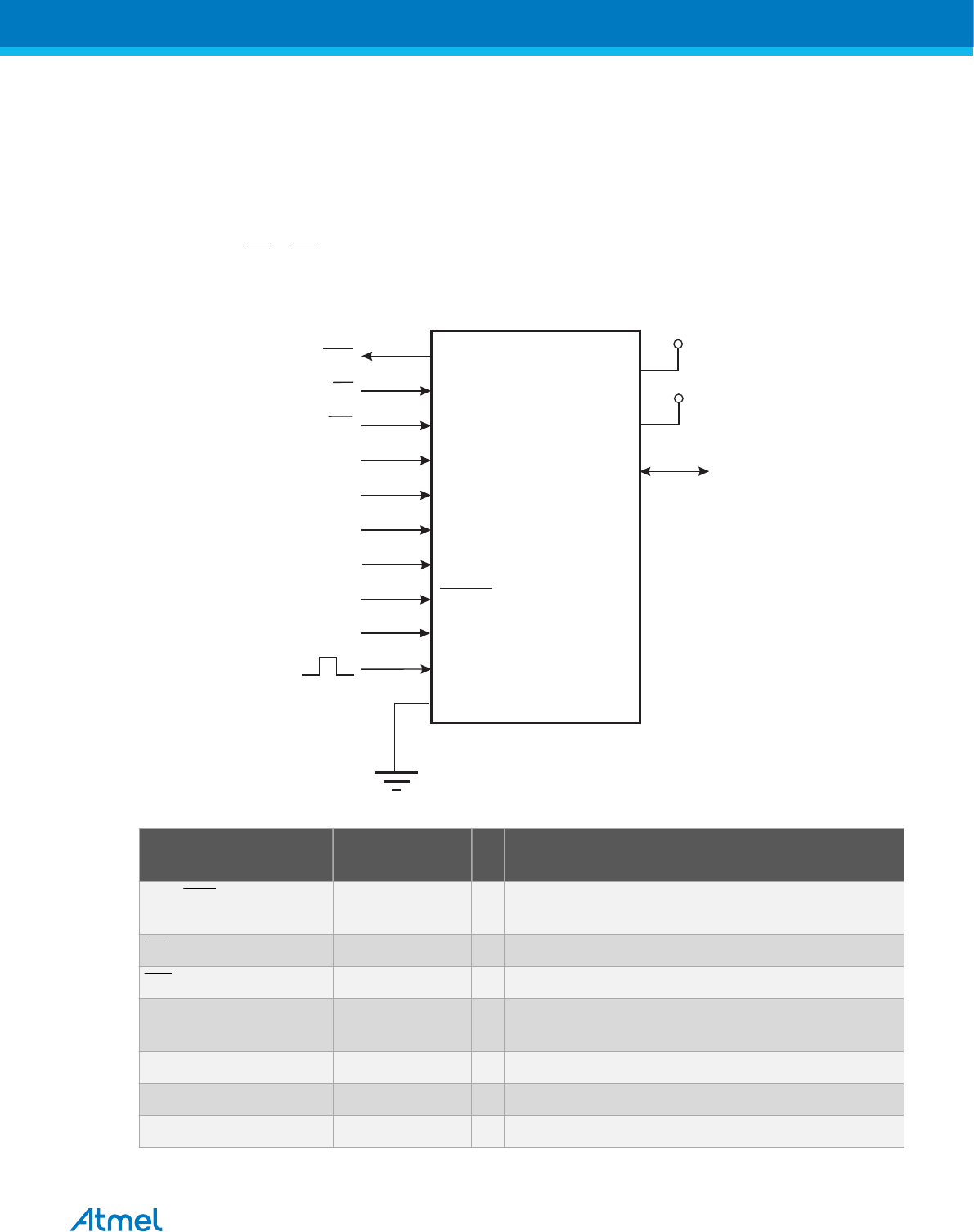
29.6.1. Signal Names
In this section, some pins of this device are referenced by signal names describing their functionality
during parallel programming, please refer to the following figure and table Pin Name Mapping in this
section. Pins not described in the following table are referenced by pin names.
The XA1/XA0 pins determine the action executed when the XTAL1 pin is given a positive pulse. The bit
coding is shown in the table XA1 and XA0 Coding in this section.
When pulsing WR or OE, the command loaded determines the action executed. The different Commands
are shown in the table Command Byte Bit Coding in this section.
Figure 29-1 Parallel Programming
VCC
+5V
GND
XTAL1
PD1
PD2
PD3
PD4
PD5
PD6
PC[1:0]:PB[5:0]
DATA
RESET
PD7
+12 V
BS1
XA0
XA1
OE
RDY/BSY
PAGEL
PC2
WR
BS2
AVCC
+5V
Table 29-8 Pin Name Mapping
Signal Name in
Programming Mode
Pin Name I/O Function
RDY/BSY PD1 O 0: Device is busy programming, 1: Device is ready for
new command
OE PD2 I Output Enable (Active low)
WR PD3 I Write Pulse (Active low)
BS1 PD4 I Byte Select 1 (“0” selects Low byte, “1” selects High
byte)
XA0 PD5 I XTAL Action Bit 0
XA1 PD6 I XTAL Action Bit 1
PAGEL PD7 I Program memory and EEPROM Data Page Load
Atmel ATmega8A [DATASHEET]
Atmel-8159F-8-bit AVR Microcontroller_Datasheet_Complete-09/2015
287
Signal Name in
Programming Mode
Pin Name I/O Function
BS2 PC2 I Byte Select 2 (“0” selects Low byte, “1” selects 2’nd
High byte)
DATA {PC[1:0]: PB[5:0]} I/O Bi-directional Data bus (Output when OE is low)
Table 29-9 Pin Values Used to Enter Programming Mode
Pin Symbol Value
PAGEL Prog_enable[3] 0
XA1 Prog_enable[2] 0
XA0 Prog_enable[1] 0
BS1 Prog_enable[0] 0
Table 29-10 XA1 and XA0 Coding
XA1 XA0 Action when XTAL1 is Pulsed
0 0 Load Flash or EEPROM Address (High or low address byte determined by BS1)
0 1 Load Data (High or Low data byte for Flash determined by BS1)
1 0 Load Command
1 1 No Action, Idle
Table 29-11 Command Byte Bit Coding
Command Byte Command Executed
1000 0000 Chip Erase
0100 0000 Write Fuse bits
0010 0000 Write Lock bits
0001 0000 Write Flash
0001 0001 Write EEPROM
0000 1000 Read Signature Bytes and Calibration byte
0000 0100 Read Fuse and Lock bits
0000 0010 Read Flash
0000 0011 Read EEPROM
29.7. Parallel Programming
29.7.1. Enter Programming Mode
The following algorithm puts the device in Parallel Programming mode:
1. Apply 4.5 - 5.5V between VCC and GND, and wait at least 100µs.
Atmel ATmega8A [DATASHEET]
Atmel-8159F-8-bit AVR Microcontroller_Datasheet_Complete-09/2015
288

2. Set RESET to “0” and toggle XTAL1 at least 6 times
3. Set the Prog_enable pins listed in table Pin Values Used to Enter Programming Mode to “0000” and
wait at least 100ns.
4. Apply 11.5 - 12.5V to RESET. Any activity on Prog_enable pins within 100ns after +12V has been
applied to RESET, will cause the device to fail entering Programming mode.
Note, if the RESET pin is disabled by programming the RSTDISBL Fuse, it may not be possible to follow
the proposed algorithm above. The same may apply when External Crystal or External RC configuration
is selected because it is not possible to apply qualified XTAL1 pulses. In such cases, the following
algorithm should be followed:
1. Set Prog_enable pins listed in table Pin Values Used to Enter Programming Mode to “0000”.
2. Apply 4.5 - 5.5V between VCC and GND simultaneously as 11.5 - 12.5V is applied to RESET.
3. Wait 100ns.
4. Re-program the fuses to ensure that External Clock is selected as clock source (CKSEL3:0 =
0’b0000) and RESET pin is activated (RSTDISBL unprogrammed). If Lock Bits are programmed, a
chip erase command must be executed before changing the fuses.
5. Exit Programming mode by power the device down or by bringing RESET pin to 0’b0.
6. Entering Programming mode with the original algorithm, as described above.
29.7.2. Considerations for Efficient Programming
The loaded command and address are retained in the device during programming. For efficient
programming, the following should be considered.
•The command needs only be loaded once when writing or reading multiple memory locations.
•Skip writing the data value 0xFF, that is the contents of the entire EEPROM (unless the EESAVE
Fuse is programmed) and Flash after a Chip Erase.
•Address high byte needs only be loaded before programming or reading a new 256 word window in
Flash or 256byte EEPROM. This consideration also applies to Signature bytes reading.
29.7.3. Chip Erase
The Chip Erase will erase the Flash and EEPROM memories plus Lock bits. The Lock bits are not reset
until the program memory has been completely erased. The Fuse bits are not changed. A Chip Erase
must be performed before the Flash and/or EEPROM are reprogrammed.
Note: The EEPRPOM memory is preserved during Chip Erase if the EESAVE Fuse is programmed.
Load Command “Chip Erase”:
1. Set XA1, XA0 to “10”. This enables command loading.
2. Set BS1 to “0”.
3. Set DATA to “1000 0000”. This is the command for Chip Erase.
4. Give XTAL1 a positive pulse. This loads the command.
5. Give WR a negative pulse. This starts the Chip Erase. RDY/BSY goes low.
6. Wait until RDY/BSY goes high before loading a new command.
29.7.4. Programming the Flash
The Flash is organized in pages, see Table 29-6 Number of Words in a Page and Number of Pages in
the Flash on page 286. When programming the Flash, the program data is latched into a page buffer.
This allows one page of program data to be programmed simultaneously. The following procedure
describes how to program the entire Flash memory:
Atmel ATmega8A [DATASHEET]
Atmel-8159F-8-bit AVR Microcontroller_Datasheet_Complete-09/2015
289

Step A. Load Command “Write Flash”.
1. Set XA1, XA0 to “10”. This enables command loading.
2. Set BS1 to “0”.
3. Set DATA to “0001 0000”. This is the command for Write Flash.
4. Give XTAL1 a positive pulse. This loads the command.
Step B. Load Address Low Byte.
1. Set XA1, XA0 to “00”. This enables address loading.
2. Set BS1 to “0”. This selects low address.
3. Set DATA = Address low byte (0x00 - 0xFF).
4. Give XTAL1 a positive pulse. This loads the address low byte.
Step C. Load Data Low Byte.
1. Set XA1, XA0 to “01”. This enables data loading.
2. Set DATA = Data low byte (0x00 - 0xFF).
3. Give XTAL1 a positive pulse. This loads the data byte.
Step D. Load Data High Byte.
1. Set BS1 to “1”. This selects high data byte.
2. Set XA1, XA0 to “01”. This enables data loading.
3. Set DATA = Data high byte (0x00 - 0xFF).
4. Give XTAL1 a positive pulse. This loads the data byte.
Step E. Latch Data.
1. Set BS1 to “1”. This selects high data byte.
2. Give PAGEL a positive pulse. This latches the data bytes. (Refer to figure Programming the Flash
Waveforms in this section for signal waveforms)
Step F. Repeat B through E until the entire buffer is filled or until all data within the page is loaded.
While the lower bits in the address are mapped to words within the page, the higher bits address the
pages within the FLASH. This is illustrated in the following figure, Addressing the Flash Which is
Organized in Pages, in this section. Note that if less than eight bits are required to address words in the
page (pagesize < 256), the most significant bit(s) in the address low byte are used to address the page
when performing a Page Write.
Step G. Load Address High byte.
1. Set XA1, XA0 to “00”. This enables address loading.
2. Set BS1 to “1”. This selects high address.
3. Set DATA = Address high byte (0x00 - 0xFF).
4. Give XTAL1 a positive pulse. This loads the address high byte.
Step H. Program Page.
1. Set BS1 = “0”
2. Give WR a negative pulse. This starts programming of the entire page of data. RDY/BSY goes low.
3. Wait until RDY/BSY goes high (Refer to figure Programming the Flash Waveforms in this section).
Atmel ATmega8A [DATASHEET]
Atmel-8159F-8-bit AVR Microcontroller_Datasheet_Complete-09/2015
290
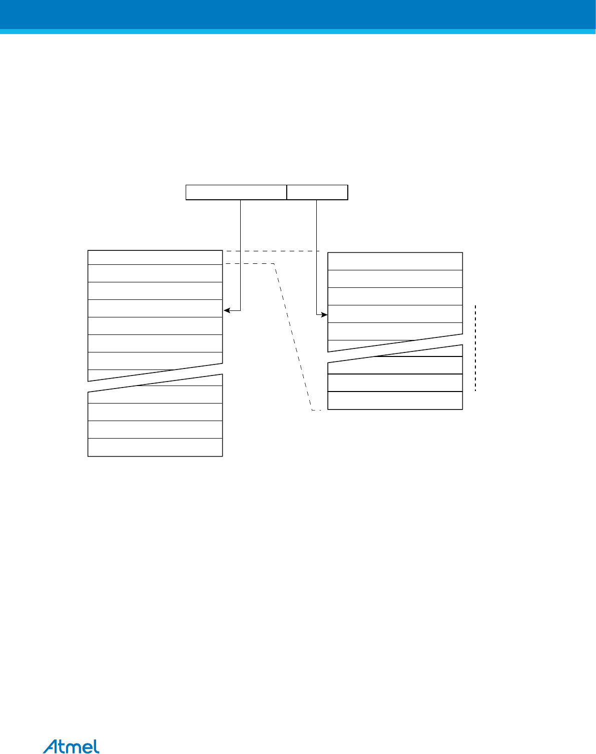
Step I. Repeat B through H until the entire Flash is programmed or until all data has been
programmed.
Step J. End Page Programming.
1. 1. Set XA1, XA0 to “10”. This enables command loading.
2. Set DATA to “0000 0000”. This is the command for No Operation.
3. Give XTAL1 a positive pulse. This loads the command, and the internal write signals are reset.
Figure 29-2 Addressing the Flash Which is Organized in Pages
PROGRAM MEMORY
WORD ADDRESS
WITHIN A PAGE
PAGE ADDRESS
WITHIN THE FLASH
INSTRUCTION WORD
PAGE PCWORD[PAGEMSB:0]:
00
01
02
PAGEEND
PAGE
PCWORDPCPAGE
PCMSB PAGEMSB
PROGRAM
COUNTER
Note: PCPAGE and PCWORD are listed in Page Size on page 286; Table 29-6 Number of Words in a
Page and Number of Pages in the Flash on page 286 and Table 29-7 Number of Words in a Page and
Number of Pages in the EEPROM on page 286.
Atmel ATmega8A [DATASHEET]
Atmel-8159F-8-bit AVR Microcontroller_Datasheet_Complete-09/2015
291
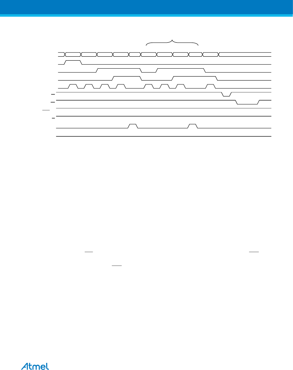
Figure 29-3 Programming the Flash Waveform
RDY/BSY
WR
OE
RESET +12V
PAGEL
BS2
0x10 ADDR. LOW ADDR. HIGH
DATA DATA LOW DATA HIGH ADDR. LOW DATA LOW DATA HIGH
XA1
XA0
BS1
XTAL1
XX XX XX
A B C D E B C D E G H
F
Note: “XX” is don’t care. The letters refer to the programming description above.
29.7.5. Programming the EEPROM
The EEPROM is organized in pages, see Page Size on page 286, Table 29-7 Number of Words in a
Page and Number of Pages in the EEPROM on page 286. When programming the EEPROM, the
program data is latched into a page buffer. This allows one page of data to be programmed
simultaneously. The programming algorithm for the EEPROM data memory is as follows (For details on
Command, Address and Data loading, refer to Programming the Flash on page 289):
1. Step A: Load Command “0001 0001”.
2. Step G: Load Address High Byte (0x00 - 0xFF).
3. Step B: Load Address Low Byte (0x00 - 0xFF).
4. Step C: Load Data (0x00 - 0xFF).
5. Step E: Latch data (give PAGEL a positive pulse).
6. Step K:Repeat 3 through 5 until the entire buffer is filled.
7. Step L: Program EEPROM page
7.1. Set BS1 to “0”.
7.2. Give WR a negative pulse. This starts programming of the EEPROM page. RDY/BSY goes
low.
7.3. Wait until to RDY/BSY goes high before programming the next page. Refer to the figure
below for signal waveforms.
Atmel ATmega8A [DATASHEET]
Atmel-8159F-8-bit AVR Microcontroller_Datasheet_Complete-09/2015
292
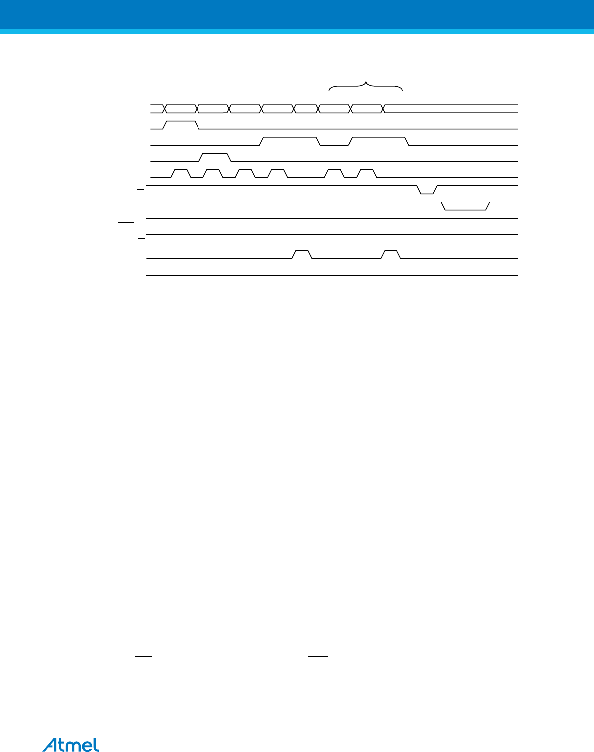
Figure 29-4 Programming the EEPROM Waveforms
RDY/BSY
WR
OE
RESET +12V
PAGEL
BS2
0x11 ADDR. HIGH
DATA ADDR. LOW DATA ADDR. LOW DATA XX
XA1
XA0
BS1
XTAL1
XX
A G B C E B C E L
K
29.7.6. Reading the Flash
The algorithm for reading the Flash memory is as follows (Please refer to Programming the Flash on
page 289 in this chapter for details on Command and Address loading):
1. Step A: Load Command “0000 0010”.
2. Step G: Load Address High Byte (0x00 - 0xFF).
3. Step B: Load Address Low Byte (0x00 - 0xFF).
4. Set OE to “0”, and BS1 to “0”. The Flash word low byte can now be read at DATA.
5. Set BS1 to “1”. The Flash word high byte can now be read at DATA.
6. Set OE to “1”.
29.7.7. Reading the EEPROM
The algorithm for reading the EEPROM memory is as follows (Please refer to Programming the Flash on
page 289 for details on Command and Address loading):
1. Step A: Load Command “0000 0011”.
2. Step G: Load Address High Byte (0x00 - 0xFF).
3. Step B: Load Address Low Byte (0x00 - 0xFF).
4. Set OE to “0”, and BS1 to “0”. The EEPROM Data byte can now be read at DATA.
5. Set OE to “1”.
29.7.8. Programming the Fuse Low Bits
The algorithm for programming the Fuse Low bits is as follows (Please refer to Programming the Flash on
page 289 for details on Command and Data loading):
1. Step A: Load Command “0100 0000”.
2. Step C: Load Data Low Byte. Bit n = “0” programs and bit n = “1” erases the Fuse bit.
3. Set BS1 and BS2 to “0”.
4. Give WR a negative pulse and wait for RDY/BSY to go high.
29.7.9. Programming the Fuse High Bits
The algorithm for programming the Fuse High bits is as follows (Please refer to Programming the Flash
on page 289 for details on Command and Data loading):
Atmel ATmega8A [DATASHEET]
Atmel-8159F-8-bit AVR Microcontroller_Datasheet_Complete-09/2015
293
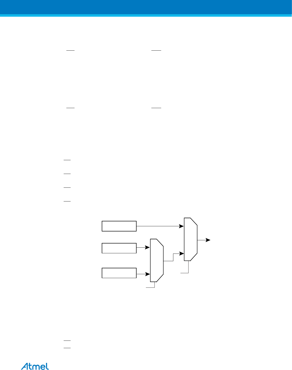
1. Step A: Load Command “0100 0000”.
2. Step C: Load Data Low Byte. Bit n = “0” programs and bit n = “1” erases the Fuse bit.
3. Set BS1 to “1” and BS2 to “0”. This selects high data byte.
4. Give WR a negative pulse and wait for RDY/BSY to go high.
5. Set BS1 to “0”. This selects low data byte.
29.7.10. Programming the Lock Bits
The algorithm for programming the Lock bits is as follows (Please refer to Programming the Flash on
page 289 for details on Command and Data loading):
1. Step A: Load Command “0010 0000”.
2. Step C: Load Data Low Byte. Bit n = “0” programs the Lock bit.
3. Give WR a negative pulse and wait for RDY/BSY to go high.
The Lock bits can only be cleared by executing Chip Erase.
29.7.11. Reading the Fuse and Lock Bits
The algorithm for reading the Fuse and Lock bits is as follows (Please refer to Programming the Flash on
page 289 for details on Command loading):
1. Step A: Load Command “0000 0100”.
2. Set OE to “0”, BS2 to “0”, and BS1 to “0”. The status of the Fuse Low bits can now be read at DATA
(“0” means programmed).
3. Set OE to “0”, BS2 to “1”, and BS1 to “1”. The status of the Fuse High bits can now be read at
DATA (“0” means programmed).
4. Set OE to “0”, BS2 to “0”, and BS1 to “1”. The status of the Lock Bits can now be read at DATA (“0”
means programmed).
5. Set OE to “1”.
Figure 29-5 Mapping Between BS1, BS2 and the Fuse and Lock Bits During Read
Fuse low byte
Lock bits 0
1
BS2
Fuse high byte
0
1
BS1
DATA
29.7.12. Reading the Signature Bytes
The algorithm for reading the Signature bytes is as follows (Please refer to Programming the Flash on
page 289 for details on Command and Address loading):
1. Step A: Load Command “0000 1000”.
2. Step B: Load Address Low Byte (0x00 - 0x02).
3. Set OE to “0”, and BS1 to “0”. The selected Signature byte can now be read at DATA.
4. Set OE to “1”.
Atmel ATmega8A [DATASHEET]
Atmel-8159F-8-bit AVR Microcontroller_Datasheet_Complete-09/2015
294
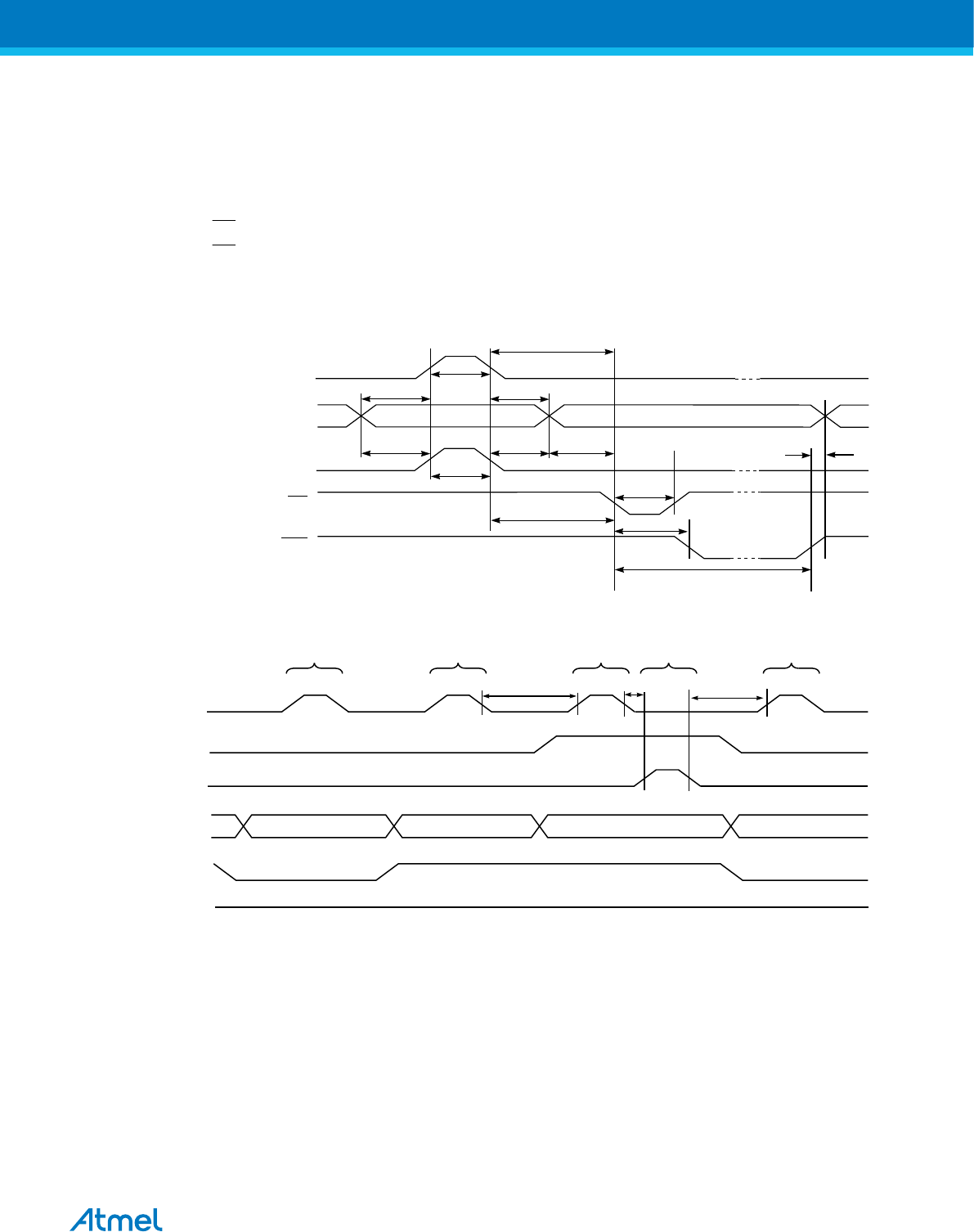
29.7.13. Reading the Calibration Byte
The algorithm for reading the Calibration byte is as follows (Please refer to Programming the Flash on
page 289 for details on Command and Address loading):
1. Step A: Load Command “0000 1000”.
2. Step B: Load Address Low byte, (0x00 - 0x03).
3. Set OE to “0”, and BS1 to “1”. The Calibration byte can now be read at DATA.
4. Set OE to “1”.
29.7.14. Parallel Programming Characteristics
Figure 29-6 Parallel Programming Timing, Including some General Timing Requirements
Data & Contol
(DATA, XA0/1, BS1, BS2)
XTAL1
tXHXL
tWLWH
tDVXH tXLDX
tPLWL
tWLRH
WR
RDY/BSY
PAGEL
tPHPL
tPLBX
tBVPH
tXLWL
tWLBX
tBVWL
WLRL
Figure 29-7 Parallel Programming Timing, Loading Sequence with Timing Requirements(1)
XTAL1
PAGEL
tPLXH
XLXH
ttXLPH
ADDR0 (Low Byte) DATA (Low Byte) DATA (High Byte) ADDR1 (Low Byte)
DATA
BS1
XA0
XA1
LOAD ADDRESS
(LOW BYTE)
LOAD DATA
(LOW BYTE)
LOAD DATA
(HIGH BYTE)
LOAD DATA
LOAD ADDRESS
(LOW BYTE)
Note: 1. The timing requirements shown in the first figure in this section (i.e., tDVXH, tXHXL, and tXLDX)
also apply to loading operation.
Atmel ATmega8A [DATASHEET]
Atmel-8159F-8-bit AVR Microcontroller_Datasheet_Complete-09/2015
295
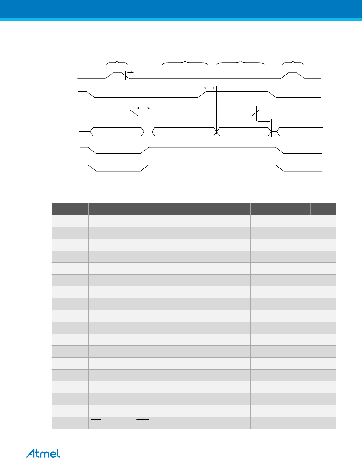
Figure 29-8 Parallel Programming Timing, Reading Sequence (within the same Page) with Timing
Requirements(1)
XTAL1
OE
ADDR0 (Low Byte) DATA (Low Byte) DATA (High Byte) ADDR1 (Low Byte)
DATA
BS1
XA0
XA1
LOAD ADDRESS
(LOW BYTE)
READ DATA
(LOW BYTE)
READ DATA
(HIGH BYTE)
LOAD ADDRESS
(LOW BYTE)
tBVDV
tOLDV
tXLOL
tOHDZ
Note: 1. The timing requirements shown in the first figure in this section (i.e., tDVXH, tXHXL, and tXLDX)
also apply to reading operation.
Table 29-12 Parallel Programming Characteristics, VCC = 5V ± 10%
Symbol Parameter Min Typ Max Units
VPP Programming Enable Voltage 11.5 12.5 V
IPP Programming Enable Current 250 μA
tDVXH Data and Control Valid before XTAL1 High 67 ns
tXLXH XTAL1 Low to XTAL1 High 200 ns
tXHXL XTAL1 Pulse Width High 150 ns
tXLDX Data and Control Hold after XTAL1 Low 67 ns
tXLWL XTAL1 Low to WR Low 0 ns
tXLPH XTAL1 Low to PAGEL high 0 ns
tPLXH PAGEL low to XTAL1 high 150 ns
tBVPH BS1 Valid before PAGEL High 67 ns
tPHPL PAGEL Pulse Width High 150 ns
tPLBX BS1 Hold after PAGEL Low 67 ns
tWLBX BS2/1 Hold after WR Low 67 ns
tPLWL PAGEL Low to WR Low 67 ns
tBVWL BS1 Valid to WR Low 67 ns
tWLWH WR Pulse Width Low 150 ns
tWLRL WR Low to RDY/BSY Low 0 1 μs
tWLRH WR Low to RDY/BSY High(1) 3.7 4.5 ms
Atmel ATmega8A [DATASHEET]
Atmel-8159F-8-bit AVR Microcontroller_Datasheet_Complete-09/2015
296
Symbol Parameter Min Typ Max Units
tWLRH_CE WR Low to RDY/BSY High for Chip Erase(2) 7.5 9 ms
tXLOL XTAL1 Low to OE Low 0 ns
tBVDV BS1 Valid to DATA valid 0 250 ns
tOLDV OE Low to DATA Valid 250 ns
tOHDZ OE High to DATA Tri-stated 250 ns
Note:
1. tWLRH is valid for the Write Flash, Write EEPROM, Write Fuse Bits and Write Lock Bits commands.
2. tWLRH_CE is valid for the Chip Erase command.
29.8. Serial Downloading
Both the Flash and EEPROM memory arrays can be programmed using the serial SPI bus while RESET
is pulled to GND. The serial interface consists of pins SCK, MOSI (input) and MISO (output). After
RESET is set low, the Programming Enable instruction needs to be executed first before program/erase
operations can be executed.
Note: The pin mapping for SPI programming is listed in the following section. Not all parts use the SPI
pins dedicated for the internal SPI interface.
29.9. Serial Programming Pin Mapping
Table 29-13 Pin Mapping Serial Programming
Symbol Pins I/O Description
MOSI PB3 I Serial Data in
MISO PB4 O Serial Data out
SCK PB5 I Serial Clock
Atmel ATmega8A [DATASHEET]
Atmel-8159F-8-bit AVR Microcontroller_Datasheet_Complete-09/2015
297
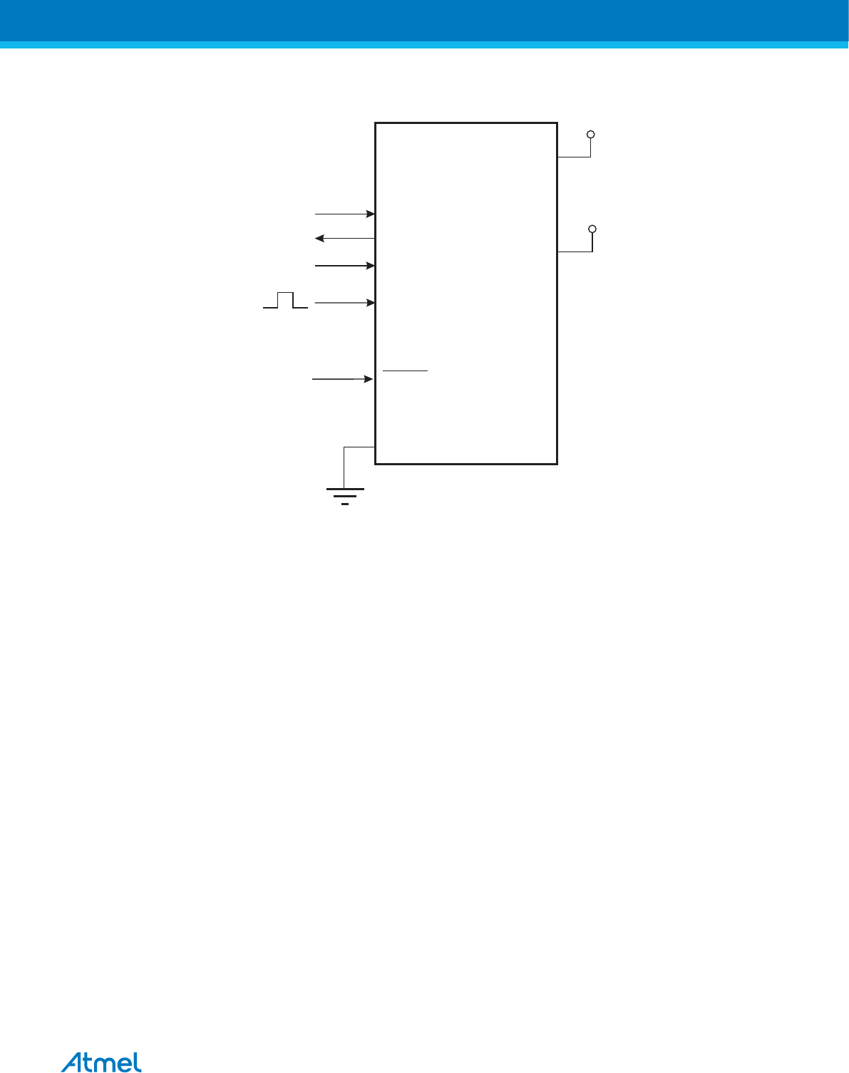
Figure 29-9 Serial Programming and Verify(1)
VCC
GND
XTAL1
SCK
MIS O
MOSI
RESET
PB3
PB4
PB5
+2.7 - 5.5V
AVCC
+2.7 - 5.5V (2)
Note:
1. If the device is clocked by the Internal Oscillator, it is no need to connect a clock source to the
XTAL1 pin.
2. VCC - 0.3 < AVCC < VCC + 0.3, however, AVCC should always be within 2.7 - 5.5V.
When programming the EEPROM, an auto-erase cycle is built into the self-timed programming operation
(in the Serial mode ONLY) and there is no need to first execute the Chip Erase instruction. The Chip
Erase operation turns the content of every memory location in both the Program and EEPROM arrays
into 0xFF.
Depending on CKSEL Fuses, a valid clock must be present. The minimum low and high periods for the
Serial Clock (SCK) input are defined as follows:
Low: > 2 CPU clock cycles for fck < 12MHz, 3 CPU clock cycles for fck ≥ 12MHz
High: > 2 CPU clock cycles for fck < 12MHz, 3 CPU clock cycles for fck ≥ 12MHz
29.9.1. Serial Programming Algorithm
When writing serial data to the ATmega8A, data is clocked on the rising edge of SCK.
When reading data from the ATmega8A, data is clocked on the falling edge of SCK. Please refer to the
figure, Serial Programming Waveforms in SPI Serial Programming Characteristics section for timing
details.
To program and verify the ATmega8A in the serial programming mode, the following sequence is
recommended (See Serial Programming Instruction set in Serial Programming Instruction Set Serial
Programming Waveforms:
1. Power-up sequence:
Atmel ATmega8A [DATASHEET]
Atmel-8159F-8-bit AVR Microcontroller_Datasheet_Complete-09/2015
298

Apply power between VCC and GND while RESET and SCK are set to “0”. In some systems, the
programmer can not guarantee that SCK is held low during power-up. In this case, RESET must be
given a positive pulse of at least two CPU clock cycles duration after SCK has been set to “0”.
2. Wait for at least 20ms and enable serial programming by sending the Programming Enable serial
instruction to pin MOSI.
3. The serial programming instructions will not work if the communication is out of synchronization.
When in sync. the second byte (0x53), will echo back when issuing the third byte of the
Programming Enable instruction. Whether the echo is correct or not, all four bytes of the instruction
must be transmitted. If the 0x53 did not echo back, give RESET a positive pulse and issue a new
Programming Enable command.
4. The Flash is programmed one page at a time. The memory page is loaded one byte at a time by
supplying the 5 LSB of the address and data together with the Load Program Memory Page
instruction. To ensure correct loading of the page, the data low byte must be loaded before data
high byte is applied for a given address. The Program Memory Page is stored by loading the Write
Program Memory Page instruction with the 7 MSB of the address. If polling is not used, the user
must wait at least tWD_FLASH before issuing the next page.
5. Note: If other commands than polling (read) are applied before any write operation (FLASH,
EEPROM, Lock Bits, Fuses) is completed, it may result in incorrect programming.
6. The EEPROM array is programmed one byte at a time by supplying the address and data together
with the appropriate Write instruction. An EEPROM memory location is first automatically erased
before new data is written. If polling is not used, the user must wait at least tWD_EEPROM before
issuing the next byte. In a chip erased device, no 0xFFs in the data file(s) need to be programmed.
7. Any memory location can be verified by using the Read instruction which returns the content at the
selected address at serial output MISO.
8. At the end of the programming session, RESET can be set high to commence normal operation.
9. Power-off sequence (if needed):
Set RESET to “1”.
Turn VCC power off.
29.9.2. Data Polling Flash
When a page is being programmed into the Flash, reading an address location within the page being
programmed will give the value 0xFF. At the time the device is ready for a new page, the programmed
value will read correctly. This is used to determine when the next page can be written. Note that the entire
page is written simultaneously and any address within the page can be used for polling. Data polling of
the Flash will not work for the value 0xFF, so when programming this value, the user will have to wait for
at least tWD_FLASH before programming the next page. As a chip-erased device contains 0xFF in all
locations, programming of addresses that are meant to contain 0xFF, can be skipped. See table in next
section for tWD_FLASH value.
29.9.3. Data Polling EEPROM
When a new byte has been written and is being programmed into EEPROM, reading the address location
being programmed will give the value 0xFF. At the time the device is ready for a new byte, the
programmed value will read correctly. This is used to determine when the next byte can be written. This
will not work for the value 0xFF, but the user should have the following in mind: As a chip-erased device
contains 0xFF in all locations, programming of addresses that are meant to contain 0xFF, can be skipped.
This does not apply if the EEPROM is Reprogrammed without chip-erasing the device. In this case, data
polling cannot be used for the value 0xFF, and the user will have to wait at least tWD_EEPROM before
programming the next byte. See table below for tWD_EEPROM value.
Atmel ATmega8A [DATASHEET]
Atmel-8159F-8-bit AVR Microcontroller_Datasheet_Complete-09/2015
299
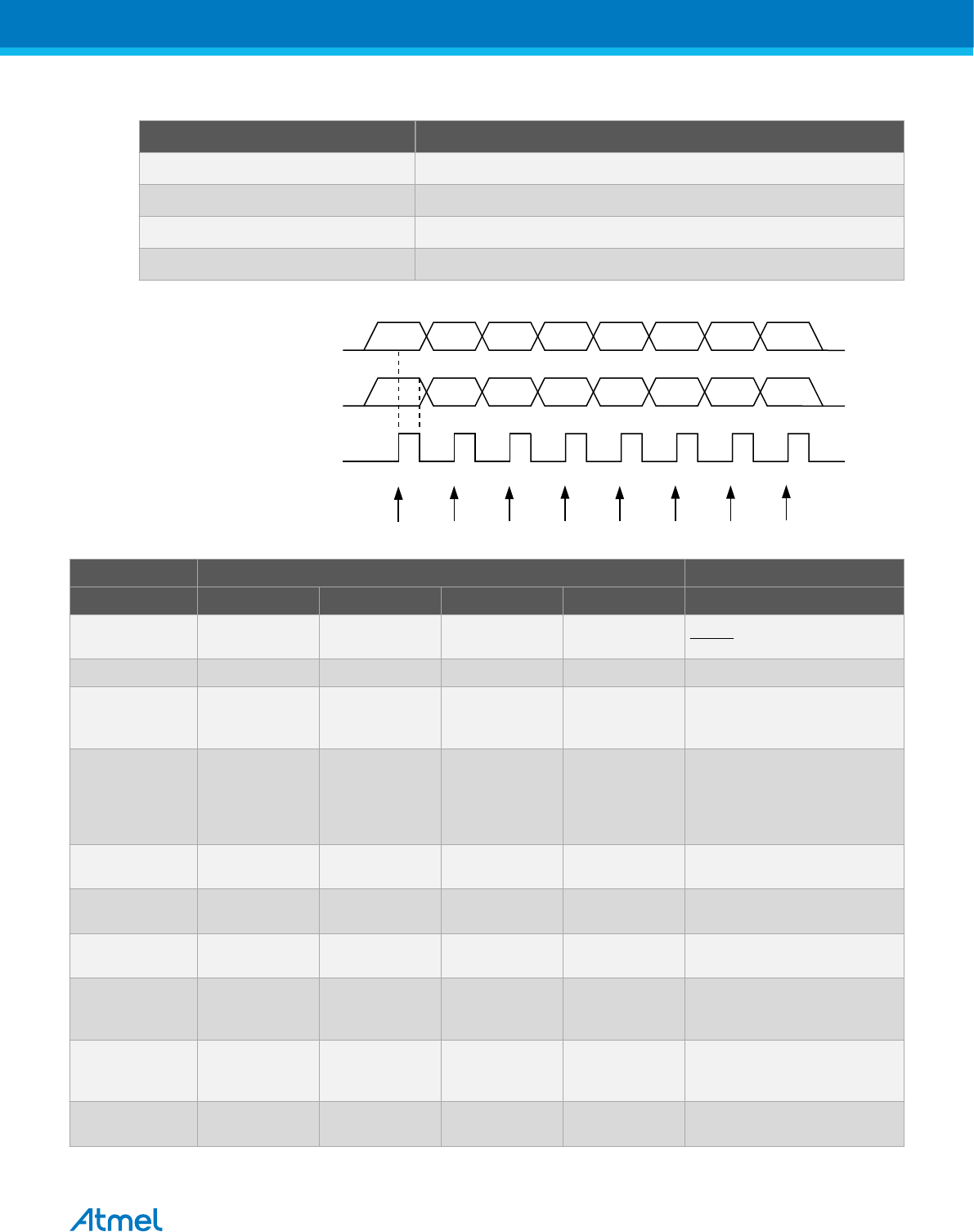
Table 29-14 Minimum Wait Delay Before Writing the Next Flash or EEPROM Location
Symbol Minimum Wait Delay
tWD_FUSE 4.5ms
tWD_FLASH 4.5ms
tWD_EEPROM 9.0ms
tWD_ERASE 9.0ms
Figure 29-10 Serial Programming Waveforms
MSB
MSB
LSB
LSB
SERIAL CLOCK INPUT
(SCK)
SERIAL DATA INPUT
(MOSI)
(MISO)
SAMPLE
SERIAL DATA OUTPUT
Table 29-15 Serial Programming Instruction Set
Instruction Format
Instruction Byte 1 Byte 2 Byte 3 Byte 4 Operation
Programming
Enable
1010 1100 0101 0011 xxxx xxxx xxxx xxxx Enable Serial Programming after
RESET goes low.
Chip Erase 1010 1100 100x xxxx xxxx xxxx xxxx xxxx Chip Erase EEPROM and Flash.
Read Program
Memory
0010 H000 0000 aaaa bbbb bbbb oooo oooo Read H (high or low) data o from
Program memory at word address
a:b.
Load Program
Memory Page
0100 H000 0000 xxxx xxxb bbbb iiii iiii Write H (high or low) data i to
Program memory page at word
address b. Data Low byte must be
loaded before Data High byte is
applied within the same address.
Write Program
Memory Page
0100 1100 0000 aaaa bbbx xxxx xxxx xxxx Write Program memory Page at
address a:b.
Read EEPROM
Memory
1010 0000 00xx xxxa bbbb bbbb oooo oooo Read data o from EEPROM
memory at address a:b.
Write EEPROM
Memory
1100 0000 00xx xxxa bbbb bbbb iiii iiii Write data i to EEPROM memory at
address a:b.
Read Lock Bits 0101 1000 0000 0000 xxxx xxxx xxoo oooo Read Lock Bits. “0” = programmed,
“1” = unprogrammed. See Table
Lock Bit Byte for details.
Write Lock Bits 1010 1100 111x xxxx xxxx xxxx 11ii iiii Write Lock Bits. Set bits = “0” to
program Lock Bits. See Table Lock
Bit Byte for details.
Read Signature
Byte
0011 0000 00xx xxxx xxxx xxbb oooo oooo Read Signature Byte o at address
b.
Atmel ATmega8A [DATASHEET]
Atmel-8159F-8-bit AVR Microcontroller_Datasheet_Complete-09/2015
300

Instruction Format
Instruction Byte 1 Byte 2 Byte 3 Byte 4 Operation
Write Fuse Bits 1010 1100 1010 0000 xxxx xxxx iiii iiii Set bits = “0” to program, “1” to
unprogram. See Table Fuse Low
Byte for details.
Write Fuse High
Bits
1010 1100 1010 1000 xxxx xxxx iiii iiii Set bits = “0” to program, “1” to
unprogram. See Table Fuse High
Byte for details.
Read Fuse Bits 0101 0000 0000 0000 xxxx xxxx oooo oooo Read Fuse Bits. “0” = programmed,
“1” = unprogrammed. See Table
Fuse Low Byte for details.
Read Fuse High
Bits
0101 1000 0000 1000 xxxx xxxx oooo oooo Read Fuse high bits. “0” =
programmed, “1” = unprogrammed.
See Table Fuse High Byte for
details.
Read Calibration
Byte
0011 1000 00xx xxxx 0000 00bb oooo oooo Read Calibration Byte
Note:
a = address high bits
b = address low bits
H = 0 – Low byte, 1 – High byte
o = data out
i = data in
x = don’t care
29.9.4. SPI Serial Programming Characteristics
For characteristics of the SPI module, see SPI Timing Characteristics.
Related Links
SPI Timing Characteristics on page 308
Atmel ATmega8A [DATASHEET]
Atmel-8159F-8-bit AVR Microcontroller_Datasheet_Complete-09/2015
301
30. Electrical Characteristics – TA = -40°C to 85°C
Note: Typical values contained in this datasheet are based on simulations and characterization of other
AVR microcontrollers manufactured on the same process technology. Min and Max values will be
available after the device is characterized.
Table 30-1 Absolute Maximum Ratings*
Operating
Temperature
-55°C to
+125°C
*NOTICE: Stresses beyond those listed under “Absolute
Maximum Ratings” may cause permanent damage to the
device. This is a stress rating only and functional operation of
the device at these or other conditions beyond those indicated
in the operational sections of this specification is not implied.
Exposure to absolute maximum rating conditions for extended
periods may affect device reliability.
Storage Temperature -65°C to
+150°C
Voltage on any Pin
except RESET
with respect to
Ground
-0.5V to VCC
+0.5V
Voltage on RESET
with respect to
Ground
-0.5V to +13.0V
Maximum Operating
Voltage
6.0V
DC Current per I/O
Pin
40.0mA
DC Current VCC and
GND Pins
300.0mA
30.1. DC Characteristics
Table 30-2 TA = -40°C to 85°C, VCC = 2.7V to 5.5V (unless otherwise noted)
Symbol Parameter Condition Min Typ Max Units
VIL Input Low Voltage except XTAL1
and RESET pins
VCC = 2.7V - 5.5V -0.5 0.2 VCC(1) V
VIH Input High Voltage except XTAL1
and RESET pins
VCC = 2.7V - 5.5V 0.6
VCC(2)
VCC + 0.5 V
VIL1 Input Low Voltage
XTAL1 pin
VCC = 2.7V - 5.5V -0.5 0.1 VCC(1) V
VIH1 Input High Voltage
XTAL 1 pin
VCC = 2.7V - 5.5V 0.8
VCC(2)
VCC + 0.5 V
VIL2 Input Low Voltage
RESET pin
VCC = 2.7V - 5.5V -0.5 0.2 VCC V
VIH2 Input High Voltage
RESET pin
VCC = 2.7V - 5.5V 0.9
VCC(2)
VCC + 0.5 V
Atmel ATmega8A [DATASHEET]
Atmel-8159F-8-bit AVR Microcontroller_Datasheet_Complete-09/2015
302

Symbol Parameter Condition Min Typ Max Units
VIL3 Input Low Voltage
RESET pin as I/O
VCC = 2.7V - 5.5V -0.5 0.2 VCC V
VIH3 Input High Voltage
RESET pin as I/O
VCC = 2.7V - 5.5V 0.6
VCC(2)
0.7
VCC(2)
VCC + 0.5 V
VOL Output Low Voltage(3)
(Ports B,C,D)
IOL = 20mA, VCC = 5V
IOL = 10mA, VCC = 3V
0.9
0.6
V
V
VOH Output High Voltage(4)
(Ports B,C,D)
IOH = -20mA, VCC = 5V
IOH = -10mA, VCC = 3V
4.2
2.2
V
V
IIL Input Leakage
Current I/O Pin
VCC = 5.5V, pin low
(absolute value)
1 μA
IIH Input Leakage
Current I/O Pin
VCC = 5.5V, pin high
(absolute value)
1 μA
RRST Reset Pull-up Resistor 30 80 kΩ
Rpu I/O Pin Pull-up Resistor 20 50 kΩ
ICC Power Supply Current Active 4MHz, VCC = 3V 2 5 mA
Active 8MHz, VCC = 5V 6 15 mA
Idle 4MHz, VCC = 3V 0.5 2 mA
Idle 8MHz, VCC = 5V 2.2 7 mA
Power-down mode(5) WDT enabled, VCC = 3V <10 28 μA
WDT disabled, VCC = 3V <1 3 μA
VACIO Analog Comparator
Input Offset Voltage
VCC = 5V
Vin = VCC/2
40 mV
IACLK Analog Comparator
Input Leakage Current
VCC = 5V
Vin = VCC/2
-50 50 nA
tACPD Analog Comparator
Propagation Delay
VCC = 2.7V
VCC = 5.0V
750
500
ns
Note:
1. “Max” means the highest value where the pin is guaranteed to be read as low
2. “Min” means the lowest value where the pin is guaranteed to be read as high
3. Although each I/O port can sink more than the test conditions (20mA at VCC = 5V, 10mA at VCC = 3V)
under steady state conditions (non-transient), the following must be observed:
PDIP, TQFP, and QFN/MLF Package:
1] The sum of all IOL, for all ports, should not exceed 300mA.
2] The sum of all IOL, for ports C0 - C5 should not exceed 100mA.
3] The sum of all IOL, for ports B0 - B7, C6, D0 - D7 and XTAL2, should not exceed 200mA.
Atmel ATmega8A [DATASHEET]
Atmel-8159F-8-bit AVR Microcontroller_Datasheet_Complete-09/2015
303
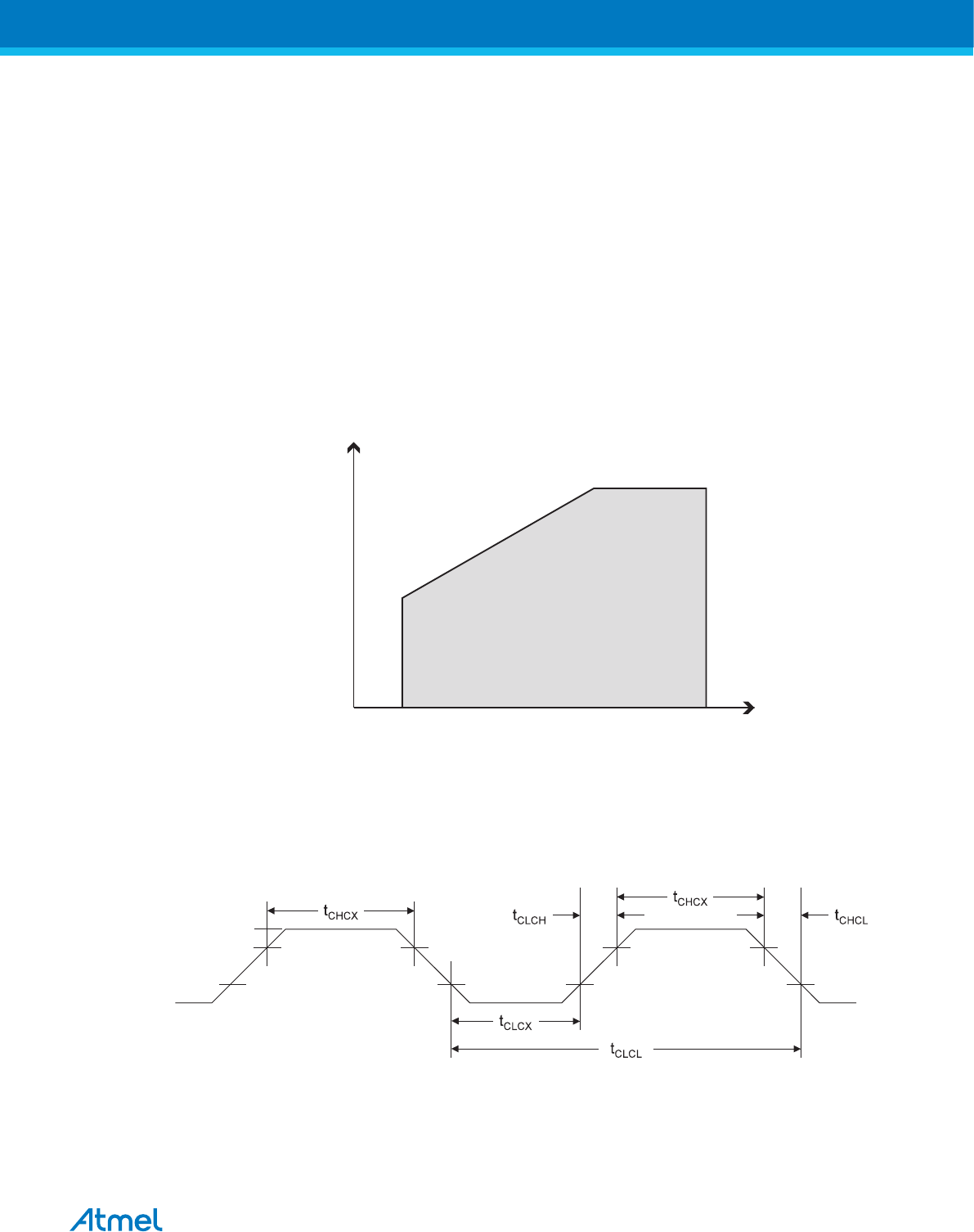
If IOL exceeds the test condition, VOL may exceed the related specification. Pins are not guaranteed to
sink current greater than the listed test condition.
4. Although each I/O port can source more than the test conditions (20mA at VCC = 5V, 10mA at VCC =
3V) under steady state conditions (non-transient), the following must be observed:
PDIP, TQFP, and QFN/MLF Package:
1] The sum of all IOH, for all ports, should not exceed 300mA.
2] The sum of all IOH, for port C0 - C5, should not exceed 100mA.
3] The sum of all IOH, for ports B0 - B7, C6, D0 - D7 and XTAL2, should not exceed 200mA.
If IOH exceeds the test condition, VOH may exceed the related specification. Pins are not guaranteed to
source current greater than the listed test condition.
5. Minimum VCC for Power-down is 2.5V.
30.2. Speed Grades
Figure 30-1 Maximum Frequency vs. Vcc
2.7V 4.5V 5.5V
Sa fe Ope rating Area
16 MHz
8 MHz
30.3. Clock Characteristics
30.3.1. External Clock Drive Waveforms
Figure 30-2 External Clock Drive Waveforms
VIL1
VIH1
Atmel ATmega8A [DATASHEET]
Atmel-8159F-8-bit AVR Microcontroller_Datasheet_Complete-09/2015
304
30.3.2. External Clock Drive
Table 30-3 External Clock Drive
Symbol Parameter VCC = 2.7V to 5.5V VCC = 4.5V to 5.5V Units
Min Max Min Max
1/tCLCL Oscillator Frequency 0 8 0 16 MHz
tCLCL Clock Period 125 62.5 ns
tCHCX High Time 50 25 ns
tCLCX Low Time 50 25 ns
tCLCH Rise Time 1.6 0.5 μs
tCHCL Fall Time 1.6 0.5 μs
ΔtCLCL Change in period from one clock cycle to the
next
2 2 %
Table 30-4 External RC Oscillator, Typical Frequencies
R [kΩ](1) C [pF] f(2)
33 22 650kHz
10 22 2.0MHz
Note:
1. R should be in the range 3kΩ - 100kΩ, and C should be at least 20pF. The C values given in the
table includes pin capacitance. This will vary with package type.
2. The frequency will vary with package type and board layout.
30.4. System and Reset Characteristics
Table 30-5 Reset, Brown-out and Internal Voltage Reference Characteristics
Symbol Parameter Condition Min Typ Max Units
VPOT Power-on Reset Threshold Voltage (rising)(1) 1.4 2.3 V
Power-on Reset Threshold Voltage (falling) 1.3 2.3 V
VRST RESET Pin Threshold Voltage 0.2 0.9 VCC
tRST Minimum pulse width on RESET Pin 1.5 μs
VBOT Brown-out Reset Threshold Voltage(2) BODLEVEL = 1 2.40 2.60 2.90 V
BODLEVEL = 0 3.70 4.00 4.50
tBOD Minimum low voltage period for Brown-out Detection BODLEVEL = 1 2 μs
BODLEVEL = 0 2 μs
VHYST Brown-out Detector hysteresis 130 mV
VBG Bandgap reference voltage 1.15 1.23 1.35 V
Atmel ATmega8A [DATASHEET]
Atmel-8159F-8-bit AVR Microcontroller_Datasheet_Complete-09/2015
305

Symbol Parameter Condition Min Typ Max Units
tBG Bandgap reference start-up time 40 70 μs
IBG Bandgap reference current consumption 10 μs
Note:
1. The Power-on Reset will not work unless the supply voltage has been below VPOT (falling).
2. VBOT may be below nominal minimum operating voltage for some devices. For devices where this
is the case, the device is tested down to VCC = VBOT during the production test. This guarantees
that a Brown-out Reset will occur before VCC drops to a voltage where correct operation of the
microcontroller is no longer guaranteed. The test is performed using BODLEVEL = 1 and
BODLEVEL = 0 for ATmega8A.
30.5. Two-wire Serial Interface Characteristics
The table below describes the requirements for devices connected to the Two-wire Serial Bus. The
ATmega8A Two-wire Serial Interface meets or exceeds these requirements under the noted conditions.
Timing symbols refer to Figure 30-3.
Table 30-6 Two-wire Serial Bus Requirements
Symbol Parameter Condition Min Max Units
VIL Input Low-voltage -0.5 0.3VCC V
VIH Input High-voltage 0.7VCC VCC + 0.5 V
Vhys(1) Hysteresis of Schmitt Trigger
Inputs
0.05VCC(2) – V
VOL(1) Output Low-voltage 3mA sink current 0 0.4 V
tr(1) Rise Time for both SDA and
SCL
20 + 0.1Cb(3)(2) 300 ns
tof(1) Output Fall Time from VIHmin to
VILmax
10pF < Cb < 400pF(3) 20 + 0.1Cb(3)(2) 250 ns
tSP(1) Spikes Suppressed by Input
Filter
0 50(2) ns
IiInput Current each I/O Pin 0.1VCC < Vi < 0.9VCC -10 10 μA
Ci(1) Capacitance for each I/O Pin – 10 pF
fSCL SCL Clock Frequency fCK(4) > max(16fSCL,
250kHz)(5)
0 400 kHz
Rp Value of Pull-up resistor fSCL ≤ 100kHz CC 0.4V
3mA
1000ns
fSCL > 100kHz CC 0.4V
3mA
300ns
Atmel ATmega8A [DATASHEET]
Atmel-8159F-8-bit AVR Microcontroller_Datasheet_Complete-09/2015
306
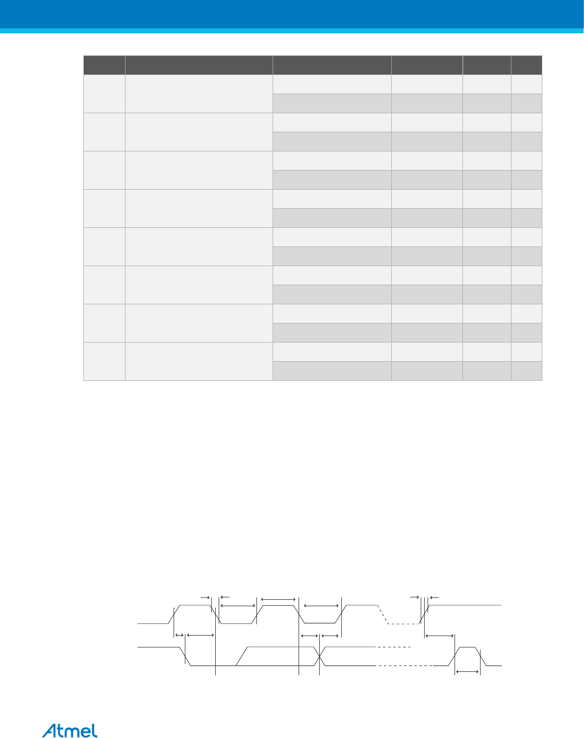
Symbol Parameter Condition Min Max Units
tHD;STA Hold Time (repeated) START
Condition
fSCL ≤ 100kHz 4.0 – μs
fSCL > 100kHz 0.6 – μs
tLOW Low Period of the SCL Clock fSCL ≤ 100kHz(6) 4.7 – μs
fSCL > 100kHz(7) 1.3 – μs
tHIGH High period of the SCL clock fSCL ≤ 100kHz 4.0 – μs
fSCL > 100kHz 0.6 – μs
tSU;STA Set-up time for a repeated
START condition
fSCL ≤ 100kHz 4.7 – μs
fSCL > 100kHz 0.6 – μs
tHD;DAT Data hold time fSCL ≤ 100kHz 0 3.45 μs
fSCL > 100kHz 0 0.9 μs
tSU;DAT Data setup time fSCL ≤ 100kHz 250 – ns
fSCL > 100kHz 100 – ns
tSU;STO Setup time for STOP condition fSCL ≤ 100kHz 4.0 – μs
fSCL > 100kHz 0.6 – μs
tBUF Bus free time between a STOP
and START condition
fSCL ≤ 100kHz 4.7 – μs
fSCL > 100kHz 1.3 – μs
Note:
1. In ATmega8A, this parameter is characterized and not 100% tested.
2. Required only for fSCL > 100kHz.
3. Cb = capacitance of one bus line in pF.
4. fCK = CPU clock frequency
5. This requirement applies to all ATmega8A Two-wire Serial Interface operation. Other devices
connected to the Two-wire Serial Bus need only obey the general fSCL requirement.
6. The actual low period generated by the ATmega8A Two-wire Serial Interface is (1/fSCL - 2/fCK), thus
fCK must be greater than 6MHz for the low time requirement to be strictly met at fSCL = 100kHz.
7. The actual low period generated by the ATmega8A Two-wire Serial Interface is (1/fSCL - 2/fCK), thus
the low time requirement will not be strictly met for fSCL > 308kHz when fCK = 8MHz. Still,
ATmega8A devices connected to the bus may communicate at full speed (400kHz) with other
ATmega8A devices, as well as any other device with a proper tLOW acceptance margin.
Figure 30-3 Two-wire Serial Bus Timing
tSU;S TA
tLOW
tHIGH
tLOW
tof
tHD;STA tHD;DAT tSU;DAT tSU;S TO
tBUF
SCL
SDA
tr
Atmel ATmega8A [DATASHEET]
Atmel-8159F-8-bit AVR Microcontroller_Datasheet_Complete-09/2015
307
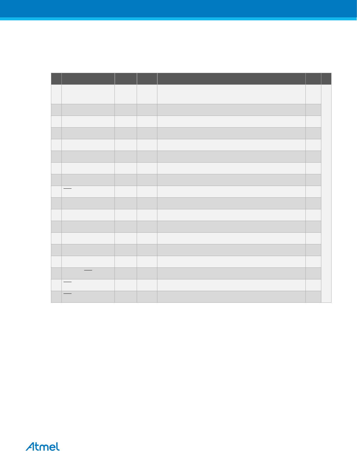
30.6. SPI Timing Characteristics
See figures below for details.
Table 30-7 SPI Timing Parameters
Description Mode Min Typ Max
1 SCK period Master See Table 23-5 Relationship between SCK and
Oscillator Frequency on page 177
ns
2 SCK high/low Master 50% duty cycle
3 Rise/Fall time Master 3.6
4 Setup Master 10
5 Hold Master 10
6 Out to SCK Master 0.5 • tSCK
7 SCK to out Master 10
8 SCK to out high Master 10
9 SS low to out Slave 15
10 SCK period Slave 4 • tck
11 SCK high/low(1) Slave 2 • tck
12 Rise/Fall time Slave 1.6
13 Setup Slave 10
14 Hold Slave 10
15 SCK to out Slave 15
16 SCK to SS high Slave 20
17 SS high to tri-state Slave 10
18 SS low to SCK Salve 2 • tck
Note:
1. In SPI Programming mode the minimum SCK high/low period is:
- 2tCLCL for fCK < 12MHz
- 3tCLCL for fCK > 12MHz
Atmel ATmega8A [DATASHEET]
Atmel-8159F-8-bit AVR Microcontroller_Datasheet_Complete-09/2015
308
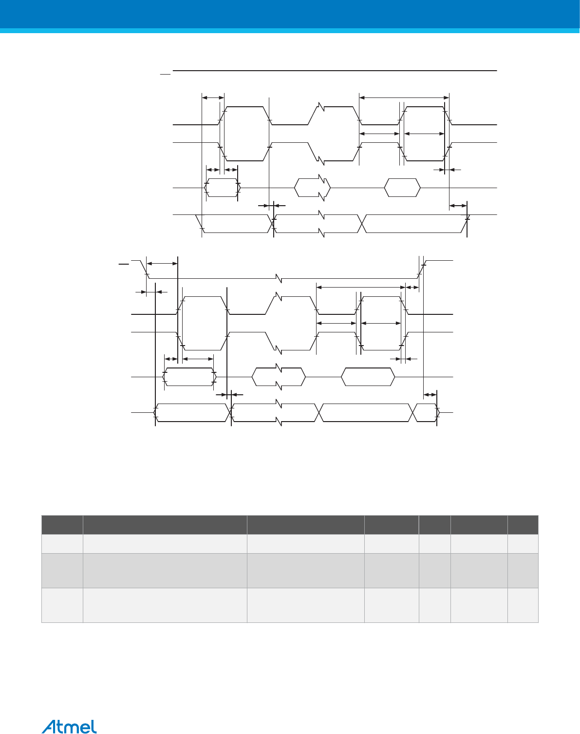
Figure 30-4 SPI interface timing requirements (Master Mode)
MOS I
(Data Output)
SCK
(CP OL = 1)
MISO
(Data Input)
SCK
(CP OL = 0)
SS
MSB LSB
LSBMSB
...
...
6 1
2 2
34 5
8
7
SPI interface timing requirements (Slave Mode)
MISO
(Data Output)
SCK
(CP OL = 1)
MOS I
(Data Input)
SCK
(CP OL = 0)
SS
MSB LSB
LSBMSB
...
...
10
11 11
1213 14
17
15
9
X
16
18
Related Links
SPCR on page 176
30.7. ADC Characteristics
Table 30-8 ADC Characteristics
Symbol Parameter Condition Min(1) Typ(1) Max(1) Units
Resolution Single Ended Conversion 10 Bits
Differential Conversion
Gain = 1x or 20x
8 Bits
Differential Conversion
Gain = 200x
7 Bits
Atmel ATmega8A [DATASHEET]
Atmel-8159F-8-bit AVR Microcontroller_Datasheet_Complete-09/2015
309

Symbol Parameter Condition Min(1) Typ(1) Max(1) Units
Absolute accuracy (Including INL,
DNL, Quantization Error, Gain, and
Offset Error)
Single Ended Conversion
VREF = 4V, VCC = 4V
ADC clock = 200kHz
1.75 LSB
Single Ended Conversion
VREF = 4V, VCC = 4V
ADC clock = 1MHz
3 LSB
Integral Non-linearity (INL) Single Ended Conversion
VREF = 4V, VCC = 4V
ADC clock = 200kHz
0.75 LSB
Differential Non-linearity (DNL) Single Ended Conversion
VREF = 4V, VCC = 4V
ADC clock = 200kHz
0.5 LSB
Gain Error Single Ended Conversion
VREF = 4V, VCC = 4V
ADC clock = 200kHz
1 LSB
Offset Error Single Ended Conversion
VREF = 4V, VCC = 4V
ADC clock = 200kHz
1 LSB
Conversion Time(4) Free Running Conversion 13 260 μs
Clock Frequency 50 1000 kHz
AVCC Analog Supply Voltage VCC - 0.3(2) VCC + 0.3(3) V
VREF Reference Voltage 2.0 AVCC V
2.0 AVCC - 0.2 V
VIN Input voltage GND VREF V
TBD TBD
Input bandwidth 38.5 kHz
Differential channels 4 kHz
VINT Internal Voltage Reference 2.3 2.56 2.8 V
RREF Reference Input Resistance 32 kΩ
RAIN Analog Input Resistance 55 100 MΩ
Note:
1. Values are guidelines only.
2. Minimum for AVCC is 2.7V.
3. Maximum for AVCC is 5.5V.
Atmel ATmega8A [DATASHEET]
Atmel-8159F-8-bit AVR Microcontroller_Datasheet_Complete-09/2015
310

4. Maximum conversion time is 1/50kHz*25 = 0.5ms.
Atmel ATmega8A [DATASHEET]
Atmel-8159F-8-bit AVR Microcontroller_Datasheet_Complete-09/2015
311
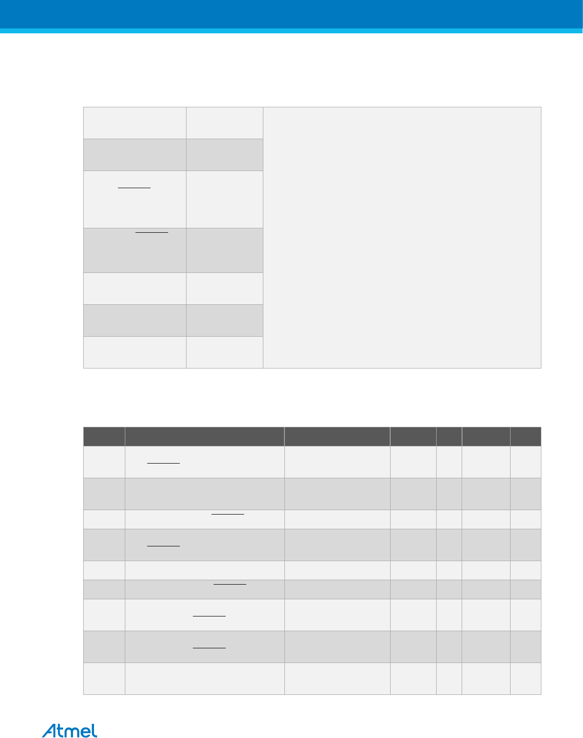
31. Electrical Characteristics – TA = -40°C to 105°C
Absolute Maximum Ratings*
Operating
Temperature
-55°C to
+125°C
*NOTICE: Stresses beyond those listed under “Absolute
Maximum Ratings” may cause permanent damage to the
device. This is a stress rating only and functional operation of
the device at these or other conditions beyond those indicated
in the operational sections of this specification is not implied.
Exposure to absolute maximum rating conditions for extended
periods may affect device reliability.
Storage Temperature -65°C to
+150°C
Voltage on any Pin
except RESET
with respect to
Ground
-0.5V to VCC
+0.5V
Voltage on RESET
with respect to
Ground
-0.5V to +13.0V
Maximum Operating
Voltage
6.0V
DC Current per I/O
Pin
40.0mA
DC Current VCC and
GND Pins
200.0mA
31.1. DC Characteristics
Table 31-1 TA = -40°C to 105°C, VCC = 2.7V to 5.5V (unless otherwise noted)
Symbol Parameter Condition Min. Typ. Max. Units
VIL Input Low Voltage, Except XTAL1
and RESET pin
VCC = 2.7V - 5.5V -0.5 0.2VCC(1) V
VIL1 Input Low Voltage,
XTAL1 pin
VCC = 2.7V - 5.5V -0.5 0.1VCC(1) V
VIL2 Input Low Voltage, RESET pin VCC = 2.7V - 5.5V -0.5 0.1VCC(1) V
VIH Input High Voltage, Except XTAL1
and RESET pins
VCC = 2.7V - 5.5V 0.6VCC(2) VCC + 0.5 V
VIH1 Input High Voltage, XTAL1 pin VCC = 2.7V - 5.5V 0.8VCC(2) VCC + 0.5 V
VIH2 Input High Voltage, RESET pin VCC = 2.7V - 5.5V 0.9VCC(2) VCC + 0.5 V
VOL Output Low Voltage(3),
Port B (except RESET)
IOL =20mA, VCC = 5V
IOL =10mA, VCC = 3V
0.8
0.6
V
VOH Output High Voltage(4),
Port B (except RESET)
IOH = -20mA, VCC = 5V
IOH = -10mA, VCC = 3V
4.0
2.2
V
IIL Input Leakage
Current I/O Pin
3 μA
Atmel ATmega8A [DATASHEET]
Atmel-8159F-8-bit AVR Microcontroller_Datasheet_Complete-09/2015
312

Symbol Parameter Condition Min. Typ. Max. Units
IIH Input Leakage
Current I/O Pin
3 μA
RRST Reset Pull-up Resistor 30 80 kΩ
RPU I/O Pin Pull-up Resistor 20 50 kΩ
VACIO Analog Comparator
Input Offset Voltage
VCC = 5V
Vin = VCC/2
20 mV
IACLK Analog Comparator
Input Leakage Current
VCC = 5V
Vin = VCC/2
-50 50 nA
Note:
1. “Max” means the highest value where the pin is guaranteed to be read as low
2. “Min” means the lowest value where the pin is guaranteed to be read as high
3. Although each I/O port can sink more than the test conditions (20mA at Vcc = 5V, 10mA at Vcc =
3V) under steady state conditions (non-transient), the following must be observed:
PDIP, TQFP, and QFN/MLF Package:
3.1. The sum of all IOL, for all ports, should not exceed 300mA.
3.2. The sum of all IOL, for ports C0 - C5 should not exceed 100mA.
3.3. The sum of all IOL, for ports B0 - B7, C6, D0 - D7 and XTAL2, should not exceed 200mA.
If IOL exceeds the test condition, VOL may exceed the related specification. Pins are not
guaranteed to sink current greater than the listed test condition.
4. Although each I/O port can source more than the test conditions (20mA at Vcc = 5V, 10mA at Vcc =
3V) under steady state conditions (non-transient), the following must be observed:
PDIP, TQFP, and QFN/MLF Package:
4.1. The sum of all IOH, for all ports, should not exceed 300mA.
4.2. The sum of all IOH, for port C0 - C5, should not exceed 100mA
4.3. The sum of all IOH, for ports B0 - B7, C6, D0 - D7 and XTAL2, should not exceed 200mA.
If IOH exceeds the test condition, VOH may exceed the related specification. Pins are not
guaranteed to source current greater than the listed test condition.
Table 31-2 ATmega8A DC Characteristics
TA = -40°C to 105°C, VCC = 1.8V to 5.5V (unless otherwise noted)
Symbol Parameter Condition Min. Typ. Max. Units
ICC
Power Supply Current Active 4MHz, VCC = 3V 6 mA
Active 8MHz, VCC = 5V 15 mA
Idle 4MHz, VCC = 3V 3 mA
Idle 8MHz, VCC = 5V 8 mA
Power-down mode(1) WDT enabled, VCC = 3V 35 μA
WDT disabled, VCC = 3V 6 μA
Note: 1. The current consumption values include input leakage current.
Atmel ATmega8A [DATASHEET]
Atmel-8159F-8-bit AVR Microcontroller_Datasheet_Complete-09/2015
313

32. Typical Characteristics – TA = -40°C to 85°C
The following charts show typical behavior. These figures are not tested during manufacturing. All current
consumption measurements are performed with all I/O pins configured as inputs and with internal pull-ups
enabled. A sine wave generator with Rail-to-Rail output is used as clock source.
The power consumption in Power-down mode is independent of clock selection.
The current consumption is a function of several factors such as: operating voltage, operating frequency,
loading of I/O pins, switching rate of I/O pins, code executed and ambient temperature. The dominating
factors are operating voltage and frequency.
The current drawn from capacitive loaded pins may be estimated (for one pin) as CL*VCC*f where CL =
load capacitance, VCC = operating voltage and f = average switching frequency of I/O pin.
The parts are characterized at frequencies higher than test limits. Parts are not guaranteed to function
properly at frequencies higher than the ordering code indicates.
The difference between current consumption in Power-down mode with Watchdog Timer enabled and
Power-down mode with Watchdog Timer disabled represents the differential current drawn by the
Watchdog Timer.
32.1. Active Supply Current
Figure 32-1 Active Supply Current vs. Frequency (0.1 - 1.0MHz)
ACTIVE S UP P LY CURRENT vs. LOW FREQUENCY
0.1 - 1.0 MHz
5.5 V
5.0 V
4.5 V
4.0 V
3.6 V
3.3 V
2.7 V
0
0.2
0.4
0.6
0.8
1
1.2
1.4
1.6
1.8
0 0.1 0.2 0.3 0.4 0.5 0.6 0.7 0.8 0.9 1
Fre quency (MHz)
ICC (mA)
Atmel ATmega8A [DATASHEET]
Atmel-8159F-8-bit AVR Microcontroller_Datasheet_Complete-09/2015
314
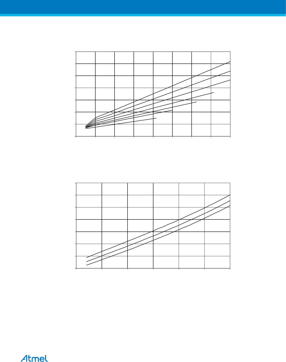
Figure 32-2 Active Supply Current vs. Frequency (1 - 16MHz)
ACTIVE S UP P LY CURRENT vs. FREQUENCY
1 - 16 MHZ
0
2
4
6
8
10
12
14
0 2 4 6 8 10 12 14 16
Fre quency (MHz)
ICC (mA)
5.5 V
5.0 V
4.5 V
4.0 V
3.6 V
3.3 V
2.7 V
Figure 32-3 Active Supply Current vs. VCC (Internal RC Oscillator, 8MHz)
ACTIVE S UP P LY CURRENT vs. VCC
INTERNAL RC OSCILLATOR, 8 MHz
85 °C
25 °C
-40 °C
3
4
5
6
7
8
9
10
2.5 3 3.5 4 4.5 5 5.5
VCC (V)
ICC (mA)
Atmel ATmega8A [DATASHEET]
Atmel-8159F-8-bit AVR Microcontroller_Datasheet_Complete-09/2015
315
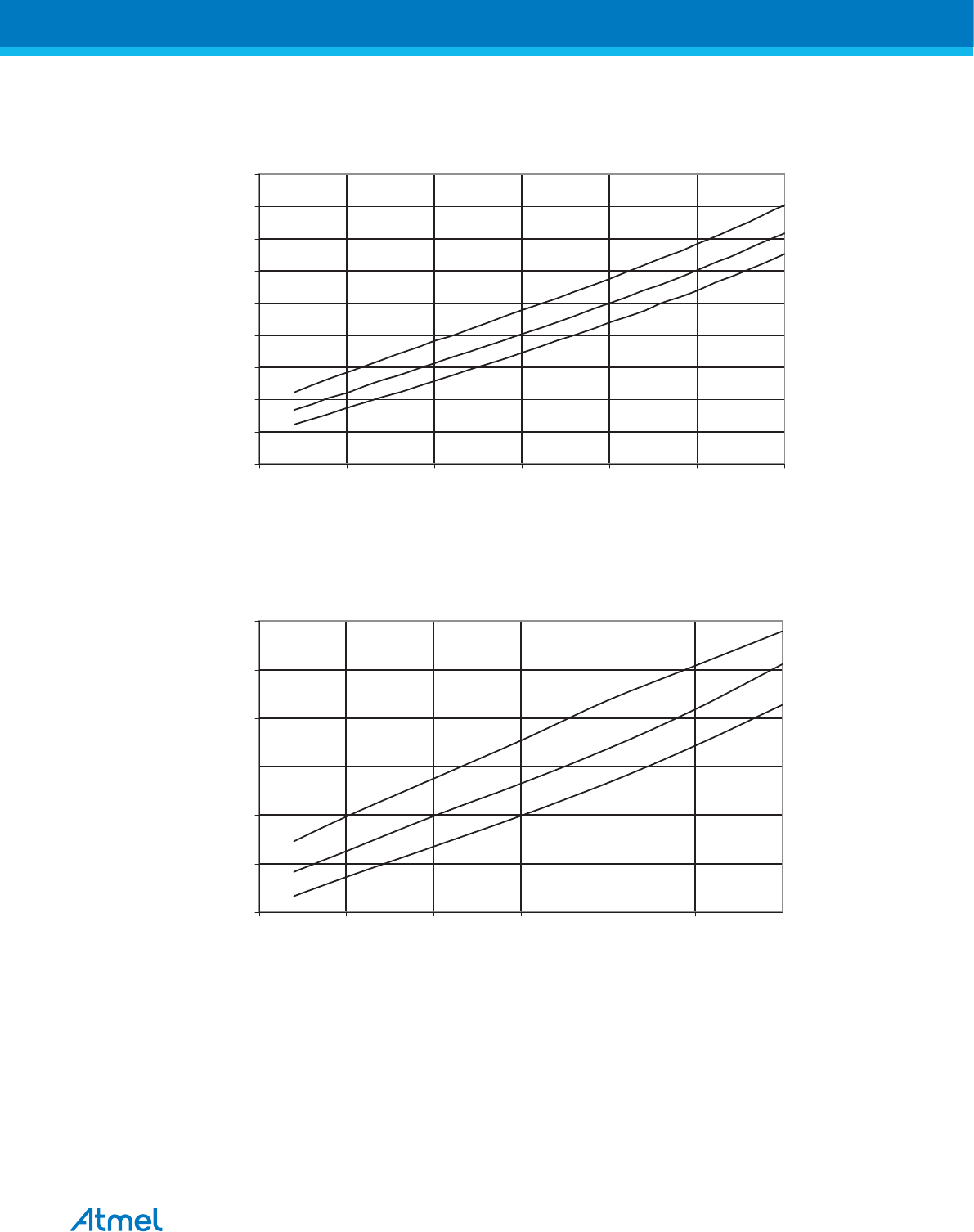
Figure 32-4 Active Supply Current vs. VCC (Internal RC Oscillator, 4MHz)
ACTIVE S UP P LY CURRENT vs. V
CC
INTERNAL RC OSCILLATOR, 4 MHz
85 °C
25 °C
-40 °C
1.5
2
2.5
3
3.5
4
4.5
5
5.5
6
2.5 3 3.5 4 4.5 5 5.5
VCC (V)
ICC (mA)
Figure 32-5 Active Supply Current vs. VCC (Internal RC Oscillator, 2MHz)
ACTIVE S UP P LY CURRENT vs. V
CC
INTERNAL RC OSCILLATOR, 2 MHz
85 °C
25 °C
-40 °C
1.2
1.6
2
2.4
2.8
3.2
3.6
2.5 3 3.5 4 4.5 5 5.5
VCC (V)
ICC (mA)
Atmel ATmega8A [DATASHEET]
Atmel-8159F-8-bit AVR Microcontroller_Datasheet_Complete-09/2015
316
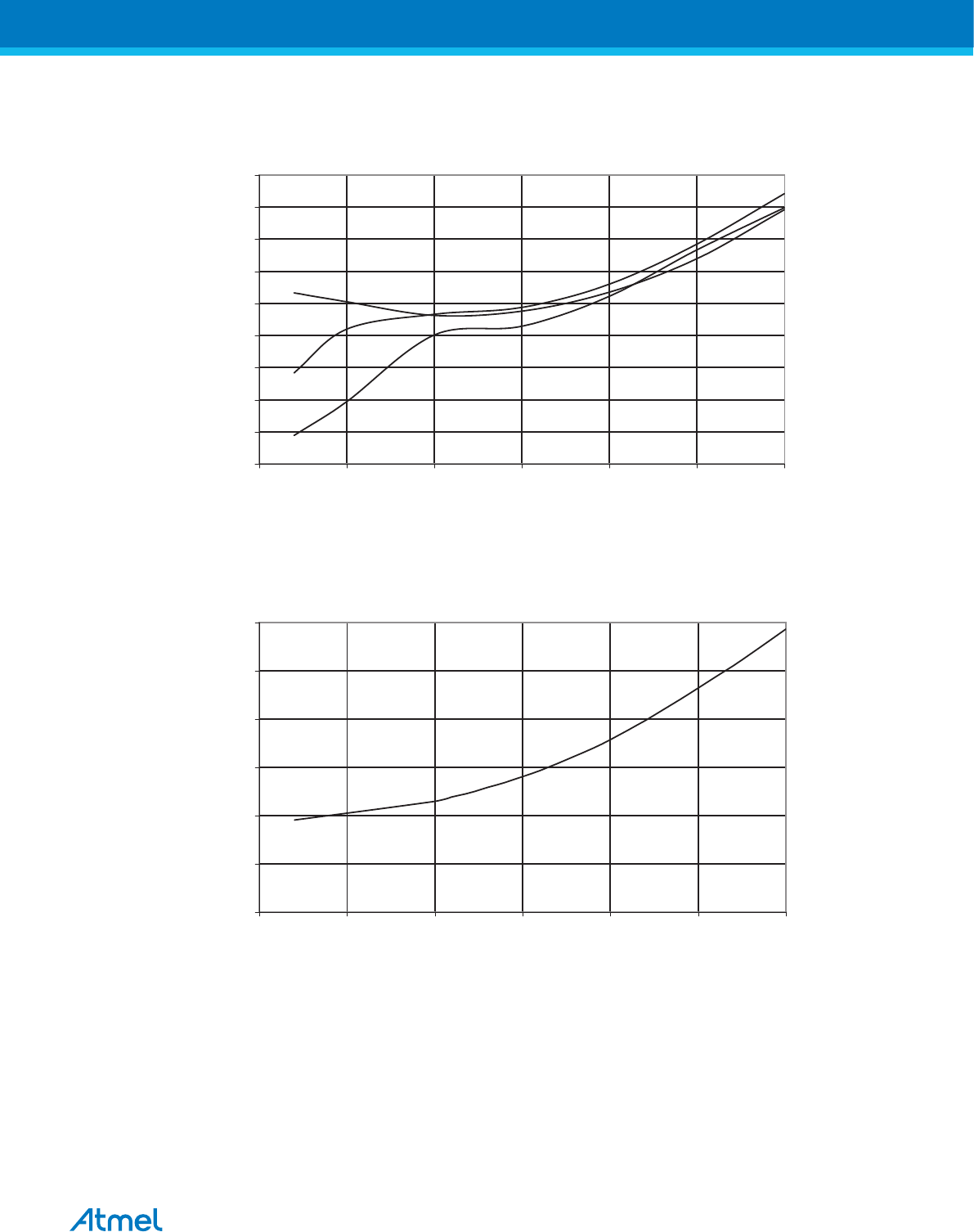
Figure 32-6 Active Supply Current vs. VCC (Internal RC Oscillator, 1MHz)
ACTIVE S UP P LY CURRENT vs. VCC
INTERNAL RC OSCILLATOR, 1 MHz
85 °C
25 °C
-40 °C
1
1.1
1.2
1.3
1.4
1.5
1.6
1.7
1.8
1.9
2.5 3 3.5 4 4.5 5 5.5
VCC (V)
ICC (mA)
Figure 32-7 Active Supply Current vs. VCC (32kHz External Oscillator)
ACTIVE S UP P LY CURRENT vs. V
CC
EXTERNAL OS CILLATOR, 32 kHz
25 °C
40
45
50
55
60
65
70
2.5 3 3.5 4 4.5 5 5.5
VCC (V)
ICC (µA)
Atmel ATmega8A [DATASHEET]
Atmel-8159F-8-bit AVR Microcontroller_Datasheet_Complete-09/2015
317
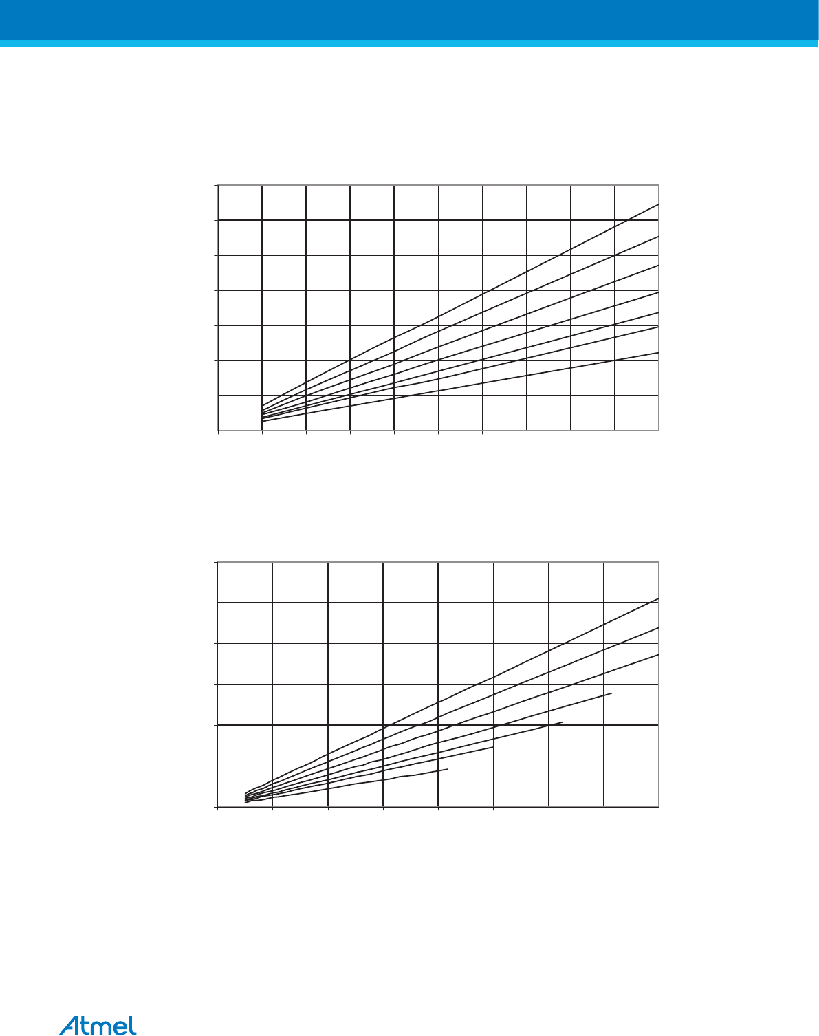
32.2. Idle Supply Current
Figure 32-8 Idle Supply Current vs. Frequency (0.1 - 1.0MHz)
IDLE S UP P LY CURRENT vs. LOW FREQUENCY
0.1 - 1.0 MHz
5.5 V
5.0 V
4.5 V
4.0 V
3.6 V
3.3 V
2.7 V
0
0.05
0.1
0.15
0.2
0.25
0.3
0.35
0 0.1 0.2 0.3 0.4 0.5 0.6 0.7 0.8 0.9 1
Fre que ncy (MHz)
ICC (mA)
Figure 32-9 Idle Supply Current vs. Frequency (1 - 16MHz)
5.5 V
5.0 V
4.5 V
4.0 V
3.6 V
3.3 V
2.7 V
IDLE S UP P LY CURRENT vs. FREQUENCY
1 - 16 MHz
0
1
2
3
4
5
6
0 2 4 6 8 10 12 14 16
Fre quency (MHz)
ICC (mA)
Atmel ATmega8A [DATASHEET]
Atmel-8159F-8-bit AVR Microcontroller_Datasheet_Complete-09/2015
318
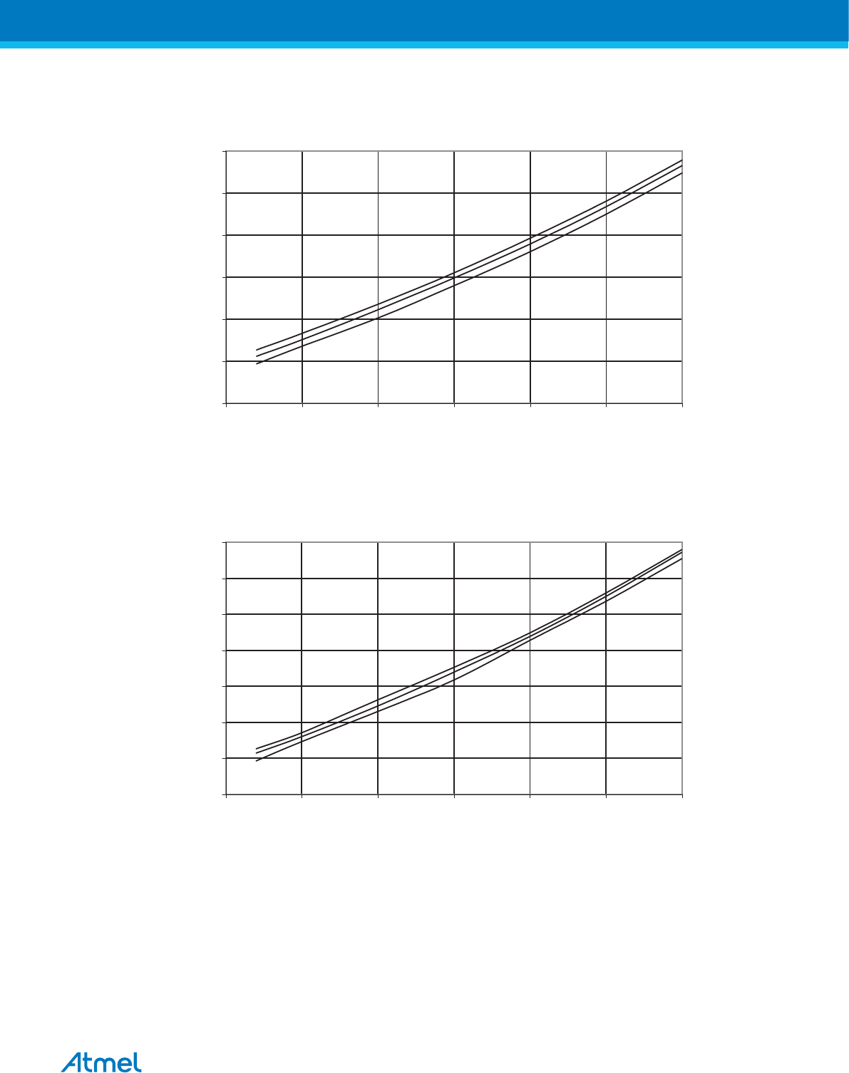
Figure 32-10 Idle Supply Current vs. VCC (Internal RC Oscillator, 8MHz)
IDLE S UP P LY CURRENT vs. V
CC
INTERNAL RC OSCILLATOR, 8 MHz
85 °C
25 °C
-40 °C
1
1.5
2
2.5
3
3.5
4
2.5 3 3.5 4 4.5 5 5.5
VCC (V)
ICC (mA)
Figure 32-11 Idle Supply Current vs. VCC (Internal RC Oscillator, 4MHz)
IDLE S UP P LY CURRENT vs. V
CC
INTERNAL RC OSCILLATOR, 4 MHz
85 °C
25 °C
-40 °C
0.6
0.8
1
1.2
1.4
1.6
1.8
2
2.5 3 3.5 4 4.5 5 5.5
VCC (V)
ICC (mA)
Atmel ATmega8A [DATASHEET]
Atmel-8159F-8-bit AVR Microcontroller_Datasheet_Complete-09/2015
319
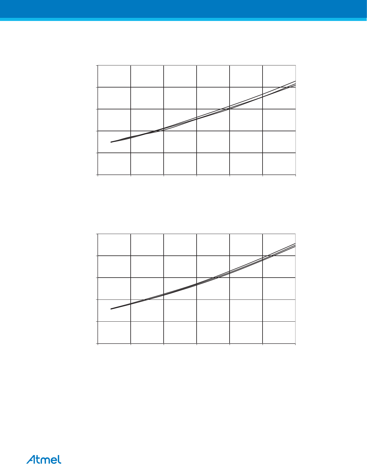
Figure 32-12 Idle Supply Current vs. VCC (Internal RC Oscillator, 2MHz)
IDLE S UP P LY CURRENT vs. V
CC
INTERNAL RC OSCILLATOR, 2 MHz
85 °C
25 °C
-40 °C
0
0.2
0.4
0.6
0.8
1
2.5 3 3.5 4 4.5 5 5.5
VCC (V)
ICC (mA)
Figure 32-13 Idle Supply Current vs. VCC (Internal RC Oscillator, 1MHz)
IDLE S UP P LY CURRENT vs. V
CC
INTERNAL RC OSCILLATOR, 1 MHz
85 °C
25 °C
-40 °C
0
0.1
0.2
0.3
0.4
0.5
2.5 3 3.5 4 4.5 5 5.5
VCC (V)
ICC (mA)
Atmel ATmega8A [DATASHEET]
Atmel-8159F-8-bit AVR Microcontroller_Datasheet_Complete-09/2015
320
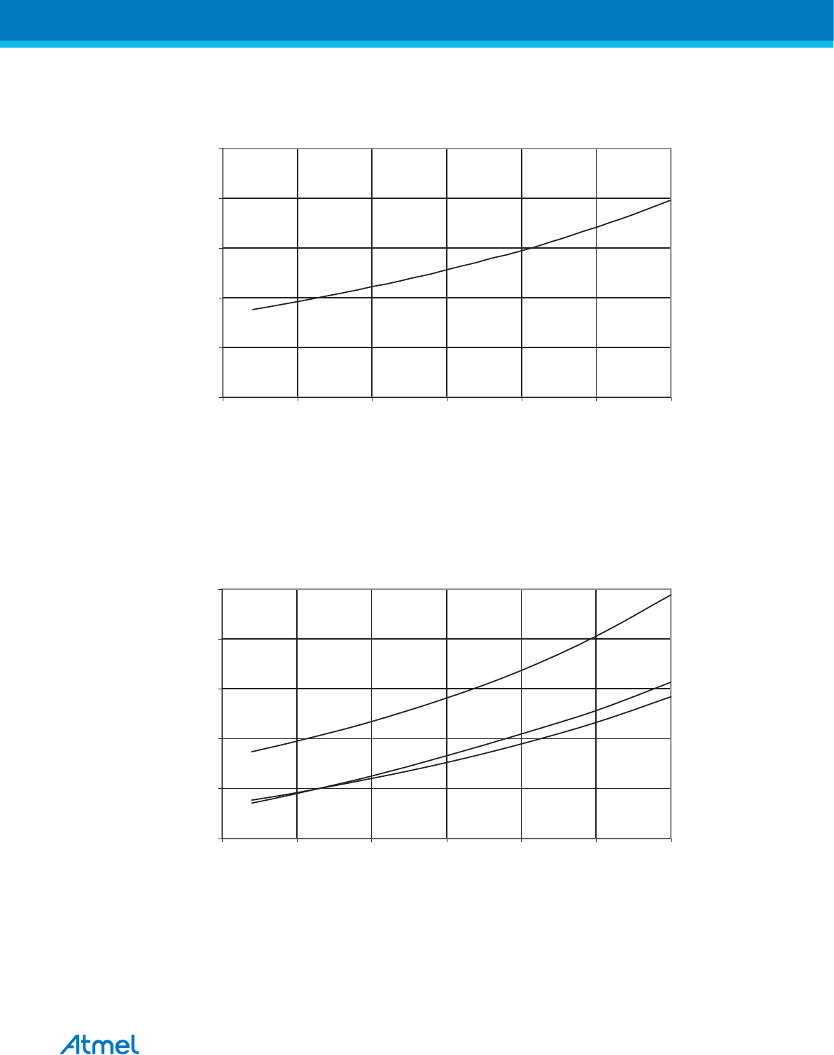
Figure 32-14 Idle Supply Current vs. VCC (32kHz External Oscillator)
IDLE S UP P LY CURRENT vs. VCC
32kHz EXTERNAL OS CILLATOR
25 °C
0
5
10
15
20
25
2.5 3 3.5 4 4.5 5 5.5
VCC (V)
ICC (uA)
32.3. Power-down Supply Current
Figure 32-15 Power-down Supply Current vs. VCC (Watchdog Timer Disabled)
POWER-DOWN S UP P LY CURRENT vs. VCC
WATCHDOG TIMER DISABLED
85 °C
25 °C
-40 °C
0
0.5
1
1.5
2
2.5
2.5 3 3.5 4 4.5 5 5.5
VCC (V)
ICC (uA)
Atmel ATmega8A [DATASHEET]
Atmel-8159F-8-bit AVR Microcontroller_Datasheet_Complete-09/2015
321
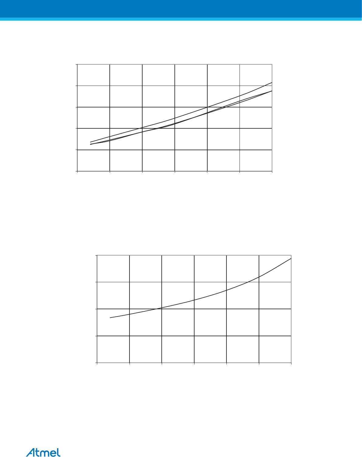
Power-down Supply Current vs. VCC (Watchdog Timer Enabled)
POWER-DOWN S UP P LY CURRENT vs. VCC
WATCHDOG TIMER ENABLED
85 °C
25 °C
-40 °C
0
5
10
15
20
25
2.5 3 3.5 4 4.5 5 5.5
VCC (V)
ICC (uA)
32.4. Power-save Supply Current
Figure 32-16 Power-save Supply Current vs. VCC (Watchdog Timer Disabled)
POWER-S AVE SUP P LY CURRENT vs. V
CC
WATCHDOG TIMER DISABLED
25 °C
2
4
6
8
10
2.5 3 3.5 4 4.5 5 5.5
VCC (V)
ICC (uA)
Atmel ATmega8A [DATASHEET]
Atmel-8159F-8-bit AVR Microcontroller_Datasheet_Complete-09/2015
322
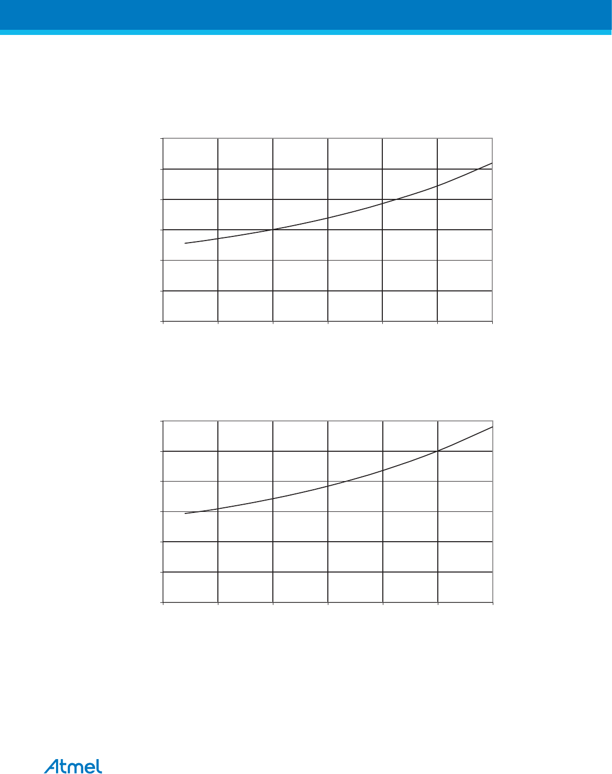
32.5. Standby Supply Current
Figure 32-17 Standby Supply Current vs. VCC (455kHz Resonator, Watchdog Timer Disabled)
STANDBY S UP P LY CURRENT vs . V
CC
450 kHZ RES ONATOR, WATCHDOG TIMER DISABLED
25 °C
0
10
20
30
40
50
60
2.5 3 3.5 4 4.5 5 5.5
VCC (V)
ICC (uA)
Figure 32-18 Standby Supply Current vs. VCC (1MHz Resonator, Watchdog Timer Disabled)
STANDBY S UP P LY CURRENT vs . VCC
1 MHz RESONATOR, WATCHDOG TIMER DISABLED
25 °C
0
10
20
30
40
50
60
2.5 3 3.5 4 4.5 5 5.5
VCC (V)
ICC (uA)
Atmel ATmega8A [DATASHEET]
Atmel-8159F-8-bit AVR Microcontroller_Datasheet_Complete-09/2015
323
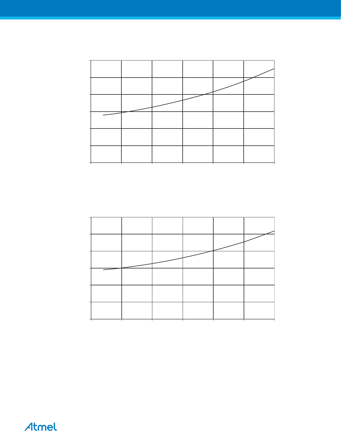
Figure 32-19 Standby Supply Current vs. VCC (1MHz Xtal, Watchdog Timer Disabled)
STANDBY S UP P LY CURRENT vs . V
CC
1 MHz XTAL, WATCHDOG TIMER DIS ABLED
25 °C
0
10
20
30
40
50
60
2.5 3 3.5 4 4.5 5 5.5
VCC (V)
ICC (uA)
Figure 32-20 Standby Supply Current vs. VCC (4MHz Resonator, Watchdog Timer Disabled)
STANDBY S UP P LY CURRENT vs . V
CC
4 MHz RESONATOR, WATCHDOG TIMER DISABLED
25 °C
0
15
30
45
60
75
90
2.5 3 3.5 4 4.5 5 5.5
VCC (V)
ICC (uA)
Atmel ATmega8A [DATASHEET]
Atmel-8159F-8-bit AVR Microcontroller_Datasheet_Complete-09/2015
324
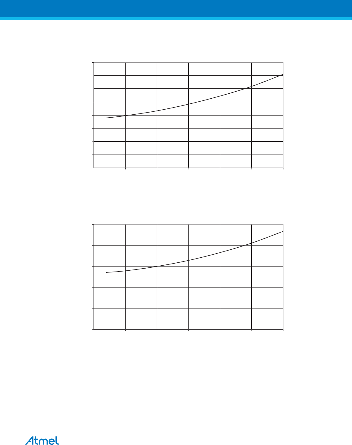
Figure 32-21 Standby Supply Current vs. VCC (4MHz Xtal, Watchdog Timer Disabled)
STANDBY S UP P LY CURRENT vs . V
CC
4 MHz XTAL, WATCHDOG TIMER DIS ABLED
25 °C
0
10
20
30
40
50
60
70
80
2.5 3 3.5 4 4.5 5 5.5
VCC (V)
ICC (uA)
Figure 32-22 Standby Supply Current vs. VCC (6MHz Resonator, Watchdog Timer Disabled)
STANDBY S UP P LY CURRENT vs . VCC
6 MHz RESONATOR, WATCHDOG TIMER DISABLED
25 °C
0
20
40
60
80
100
2.5 3 3.5 4 4.5 5 5.5
VCC (V)
ICC (uA)
Atmel ATmega8A [DATASHEET]
Atmel-8159F-8-bit AVR Microcontroller_Datasheet_Complete-09/2015
325
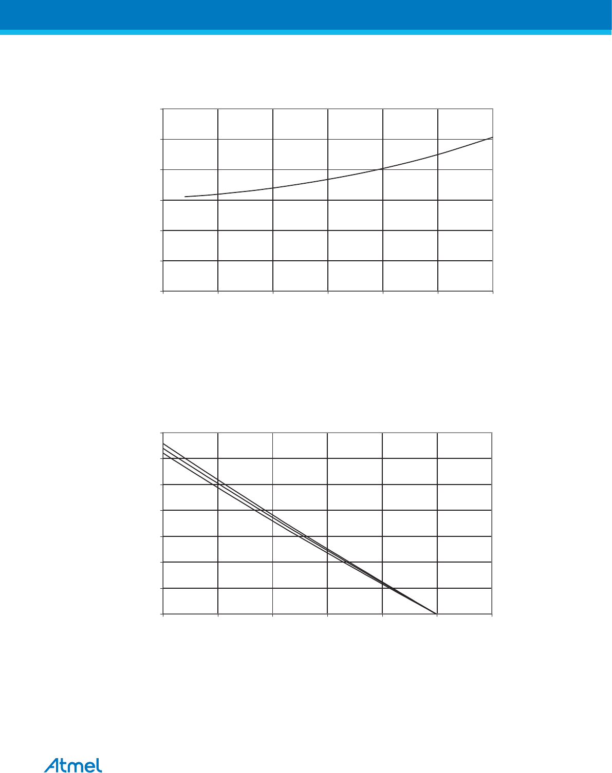
Figure 32-23 Standby Supply Current vs. VCC (6MHz Xtal, Watchdog Timer Disabled)
STANDBY S UP P LY CURRENT vs . V
CC
6 MHz XTAL, WATCHDOG TIMER DIS ABLED
25 °C
0
20
40
60
80
100
120
2.5 3 3.5 4 4.5 5 5.5
VCC (V)
ICC (uA)
32.6. Pin Pull-up
Figure 32-24 I/O Pin Pull-up Resistor Current vs. Input Voltage (VCC = 5V)
I/O PIN PULL-UP RESISTOR CURRENT vs . INPUT VOLTAGE
Vcc = 5V
0
20
40
60
80
100
120
140
0123456
VOP (V)
IOP (uA)
85 °C
25 °C
-40 °C
Atmel ATmega8A [DATASHEET]
Atmel-8159F-8-bit AVR Microcontroller_Datasheet_Complete-09/2015
326
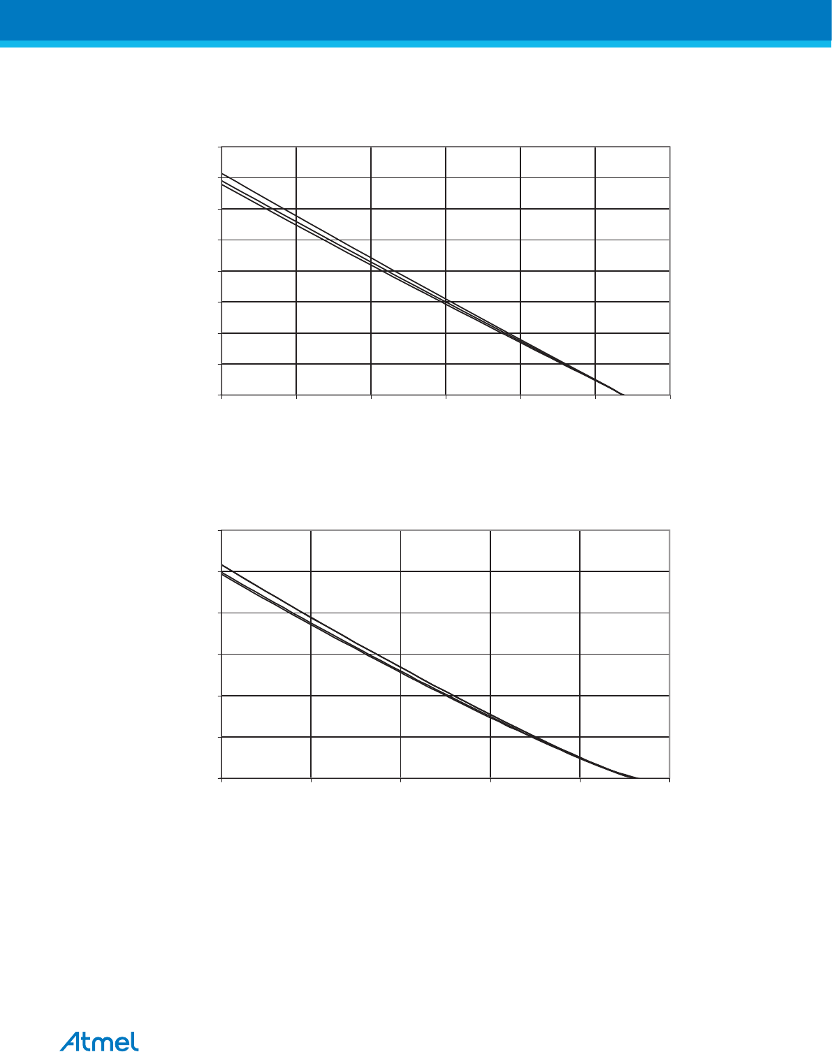
Figure 32-25 I/O Pin Pull-up Resistor Current vs. Input Voltage (VCC = 2.7V)
85 °C
25 °C
-40 °C
I/O PIN PULL-UP RESISTOR CURRENT vs . INPUT VOLTAGE
Vcc = 2.7V
0
10
20
30
40
50
60
70
80
0 0.5 1 1.5 2 2.5 3
VOP (V)
IOP (uA)
Figure 32-26 Reset Pull-up Resistor Current vs. Reset Pin Voltage (VCC = 5V)
85 °C
25 °C
-40 °C
RESET P ULL-UP RESISTOR CURRENT vs . RESET P IN VOLTAGE
Vcc = 5V
0
20
40
60
80
100
120
012345
VRES ET (V)
IRES ET (uA)
Atmel ATmega8A [DATASHEET]
Atmel-8159F-8-bit AVR Microcontroller_Datasheet_Complete-09/2015
327
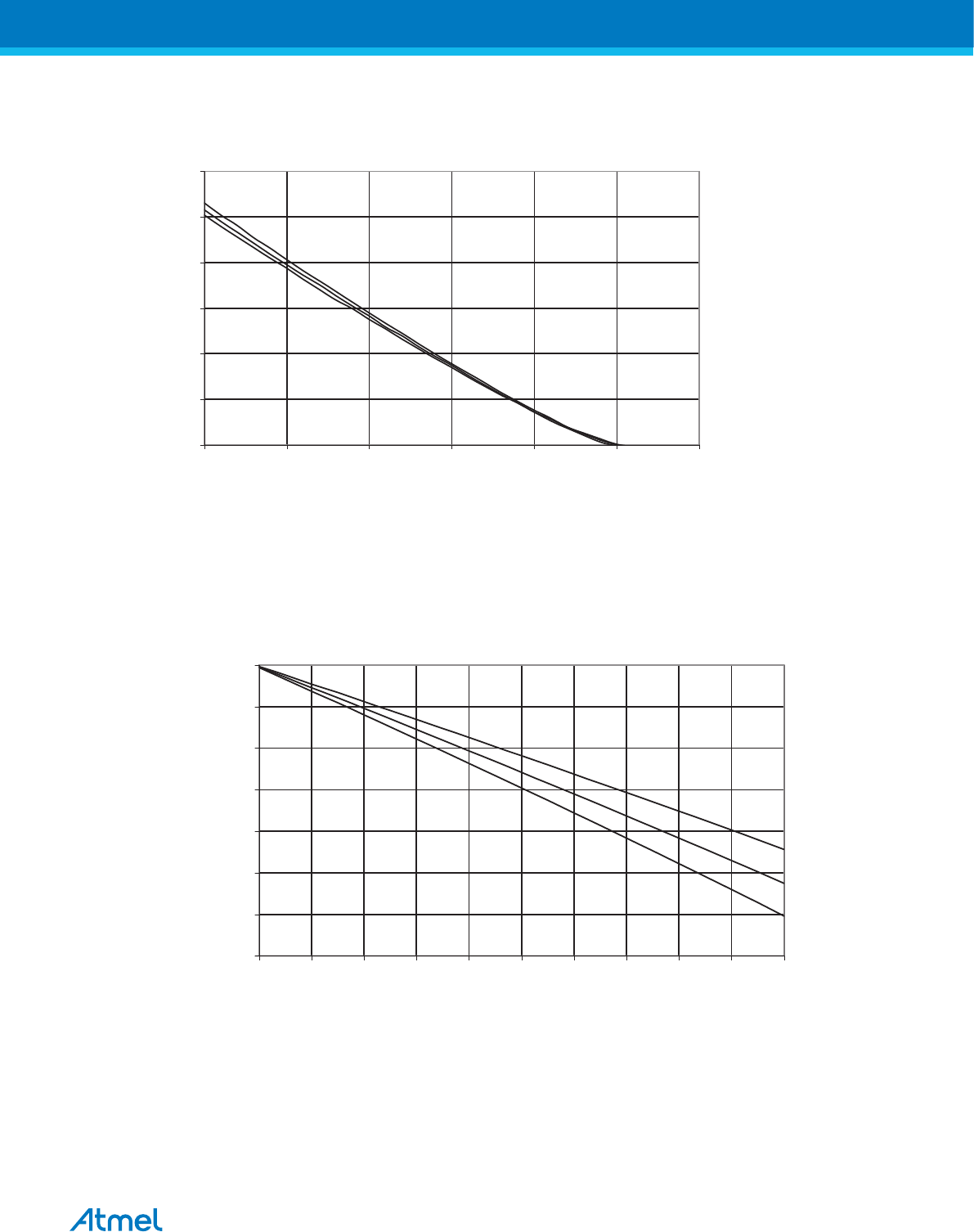
Figure 32-27 Reset Pull-up Resistor Current vs. Reset Pin Voltage (VCC = 2.7V)
85 °C
25 °C
-40 °C
RESET P ULL-UP RESISTOR CURRENT vs. RESET P IN VOLTAGE
Vcc = 2.7V
0
10
20
30
40
50
60
0 0.5 1 1.5 2 2.5 3
VRES ET (V)
IRES ET (uA)
32.7. Pin Driver Strength
Figure 32-28 I/O Pin Output Voltage vs. Source Current (VCC = 5.0V)
I/O PIN OUTP UT VOLTAGE vs . SOURCE CURRENT
VCC = 5V
85 °C
25 °C
-40 °C
4.3
4.4
4.5
4.6
4.7
4.8
4.9
5
0 2 4 6 8 10 12 14 16 18 20
IOH (mA)
VOH (V)
Atmel ATmega8A [DATASHEET]
Atmel-8159F-8-bit AVR Microcontroller_Datasheet_Complete-09/2015
328
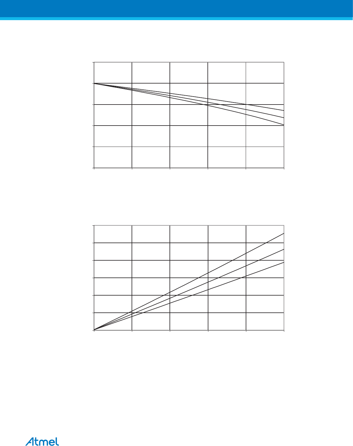
Figure 32-29 I/O Pin Output Voltage vs. Source Current (VCC = 3.0V)
I/O PIN OUTP UT VOLTAGE vs . SOURCE CURRENT
VCC = 3V
85 °C
25 °C
-40 °C
1
1.5
2
2.5
3
3.5
0 4 8 12 16 20
IOH (mA)
VOH (V)
Figure 32-30 I/O Pin Output Voltage vs. Sink Current (VCC = 5.0V)
I/O PIN OUTP UT VOLTAGE vs . SINK CURRENT
VCC = 5V
85 °C
25 °C
-40 °C
0
0.1
0.2
0.3
0.4
0.5
0.6
0 4 8 12 16 20
IOL (mA)
VOL (V)
Atmel ATmega8A [DATASHEET]
Atmel-8159F-8-bit AVR Microcontroller_Datasheet_Complete-09/2015
329
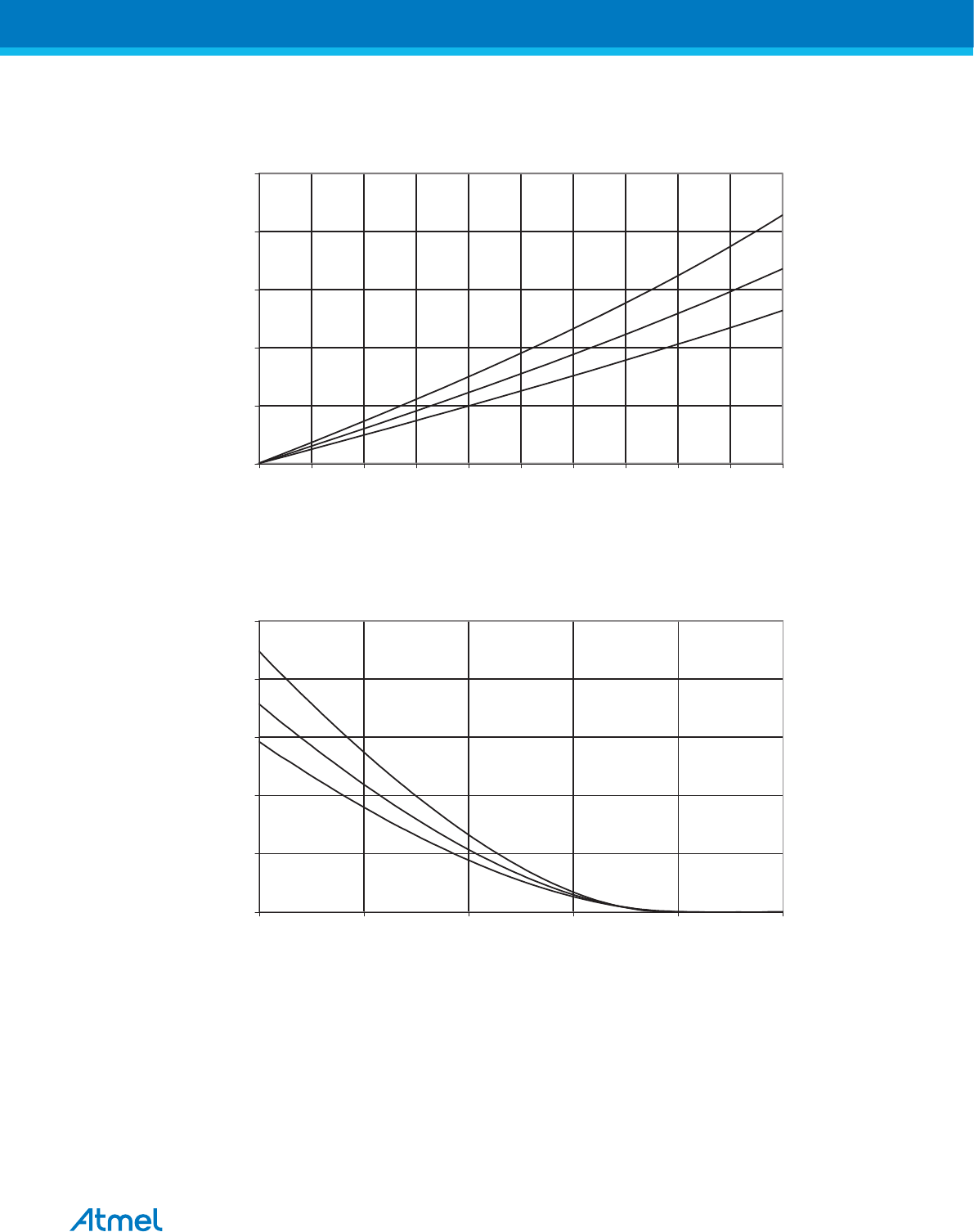
Figure 32-31 I/O Pin Output Voltage vs. Sink Current (VCC = 3.0V)
I/O PIN OUTP UT VOLTAGE vs . SINK CURRENT
VCC = 3V
85 °C
25 °C
-40 °C
0
0.2
0.4
0.6
0.8
1
0 2 4 6 8 10 12 14 16 18 20
IOL (mA)
VOL (V)
Figure 32-32 Reset Pin as I/O - Pin Source Current vs. Output Voltage (VCC = 5.0V)
RESET P IN AS I/O - SOURCE CURRENT vs. OUTP UT VOLTAGE
VCC = 5V
0
1
2
3
4
5
2 2.5 3 3.5 4 4.5
VOH (V)
Current (mA)
85 °C
25 °C
-40 °C
Atmel ATmega8A [DATASHEET]
Atmel-8159F-8-bit AVR Microcontroller_Datasheet_Complete-09/2015
330
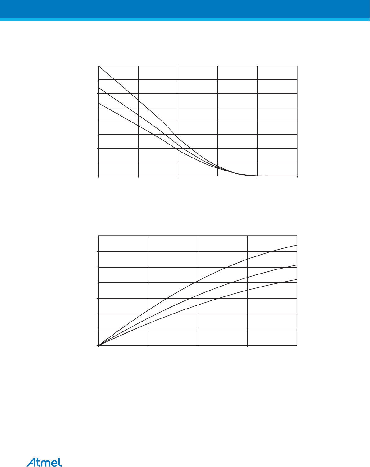
Figure 32-33 Reset Pin as I/O - Pin Source Current vs. Output Voltage (VCC = 2.7V)
RESET P IN AS I/O - SOURCE CURRENT vs. OUTP UT VOLTAGE
VCC = 2.7V
0
0.5
1
1.5
2
2.5
3
3.5
4
0 0.5 1 1.5 2 2.5
VOH (V)
Current (mA)
85 °C
25 °C
-40 °C
Figure 32-34 Reset Pin as I/O - Pin Sink Current vs. Output Voltage (VCC = 5.0V)
RESET P IN AS I/O - SINK CURRENT vs . OUTP UT VOLTAGE
VCC = 5V
85 °C
25 °C
-40 °C
0
2
4
6
8
10
12
14
0 0.5 1 1.5 2
VOL (V)
Current (mA)
Atmel ATmega8A [DATASHEET]
Atmel-8159F-8-bit AVR Microcontroller_Datasheet_Complete-09/2015
331
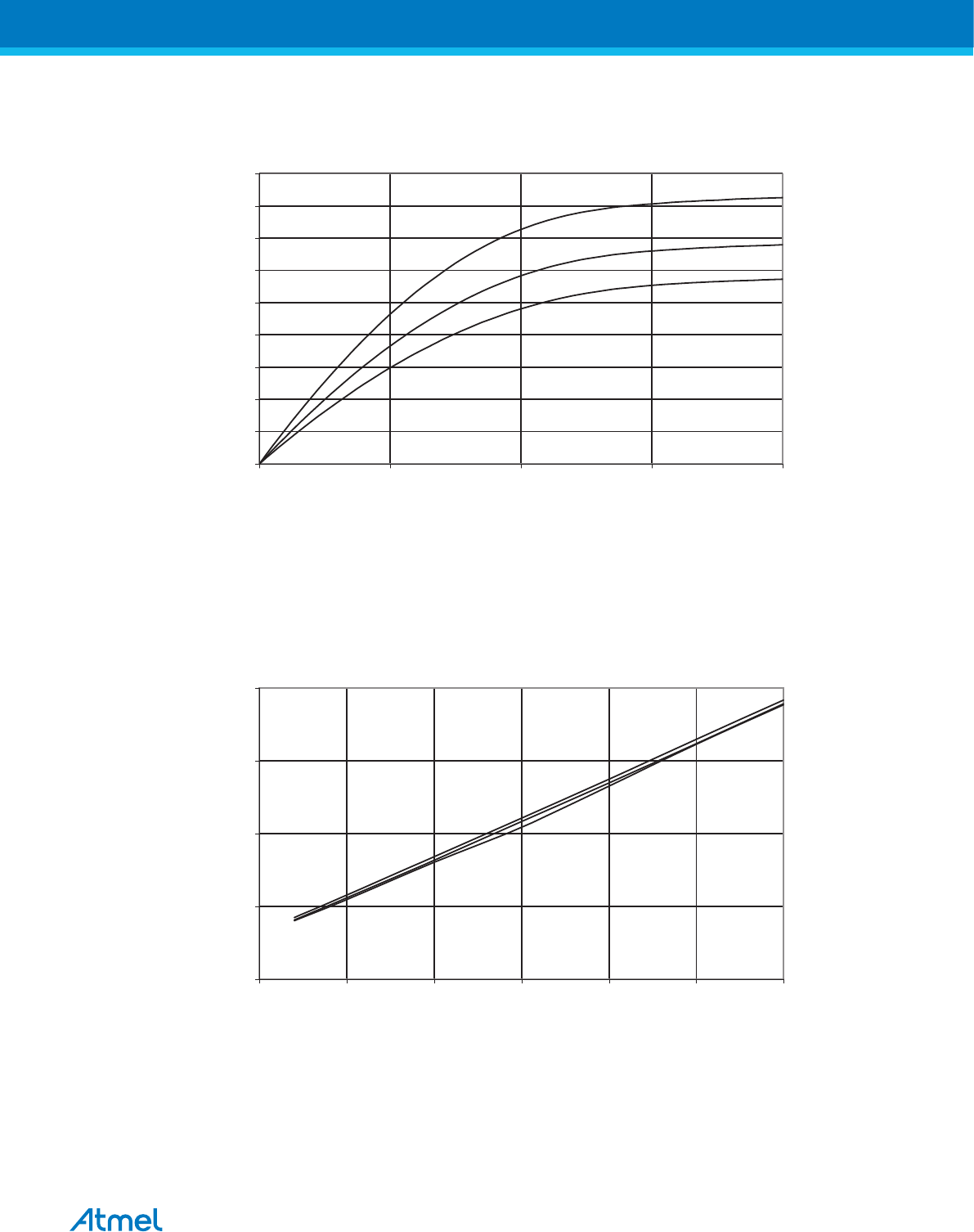
Figure 32-35 Reset Pin as I/O - Pin Sink Current vs. Output Voltage (VCC = 2.7V)
RESET P IN AS I/O - SINK CURRENT vs . OUTP UT VOLTAGE
VCC = 2.7V
85 °C
25 °C
-40 °C
0
0.5
1
1.5
2
2.5
3
3.5
4
4.5
0 0.5 1 1.5 2
VOL (V)
Current (mA)
32.8. Pin Thresholds and Hysteresis
Figure 32-36 I/O Pin Input Threshold Voltage vs. VCC (VIH, I/O Pin Read as “1”)
I/O PIN INPUT THRESHOLD VOLTAGE vs . VCC
VIH, IO P IN READ AS '1'
85 °C
25 °C
-40 °C
1
1.5
2
2.5
3
2.5 3 3.5 4 4.5 5 5.5
VCC (V)
Thres hold (V)
Atmel ATmega8A [DATASHEET]
Atmel-8159F-8-bit AVR Microcontroller_Datasheet_Complete-09/2015
332
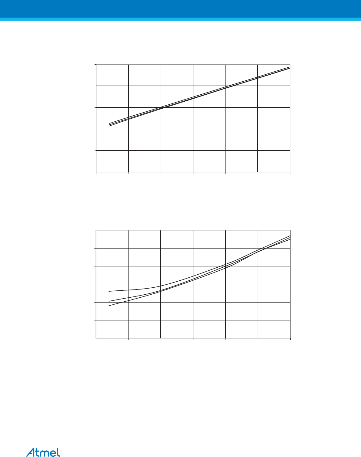
Figure 32-37 I/O Pin Input Threshold Voltage vs. VCC (VIL, I/O Pin Read as “0”)
I/O PIN INPUT THRESHOLD VOLTAGE vs . V
CC
VIL, IO P IN READ AS '0'
85 °C
25 °C
-40 °C
0
0.5
1
1.5
2
2.5
2.5 3 3.5 4 4.5 5 5.5
VCC (V)
Thres hold (V)
Figure 32-38 I/O Pin Input Hysteresis vs. VCC
I/O PIN INPUT HYSTERESIS vs. V
CC
85 °C
25 °C
-40 °C
0.2
0.25
0.3
0.35
0.4
0.45
0.5
2.5 3 3.5 4 4.5 5 5.5
VCC (V)
Input Hys tere s is (mV)
Atmel ATmega8A [DATASHEET]
Atmel-8159F-8-bit AVR Microcontroller_Datasheet_Complete-09/2015
333
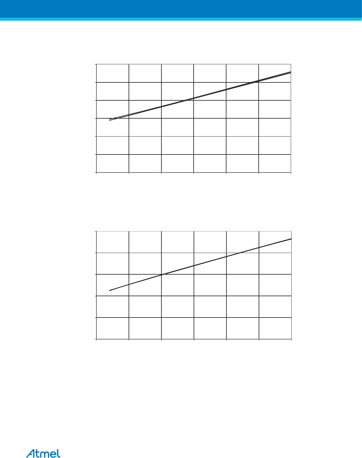
Figure 32-39 Reset Pin as I/O - Input Threshold Voltage vs. VCC (VIH, Reset Pin Read as “1”)
RESET P IN AS I/O - INPUT THRESHOLD VOLTAGE vs. V
CC
VIH, RES ET PIN READ AS '1'
85 °C
25 °C
-40 °C
0
0.5
1
1.5
2
2.5
3
2.5 3 3.5 4 4.5 5 5.5
VCC (V)
Thres hold (V)
Figure 32-40 Reset Pin as I/O - Input Threshold Voltage vs. VCC (VIL, Reset Pin Read as “0”)
RESET P IN AS I/O - INPUT THRESHOLD VOLTAGE vs. VCC
VIL, RES ET PIN READ AS '0'
85 °C
25 °C
-40 °C
0
0.5
1
1.5
2
2.5
2.5 3 3.5 4 4.5 5 5.5
VCC (V)
Thres hold (V)
Atmel ATmega8A [DATASHEET]
Atmel-8159F-8-bit AVR Microcontroller_Datasheet_Complete-09/2015
334
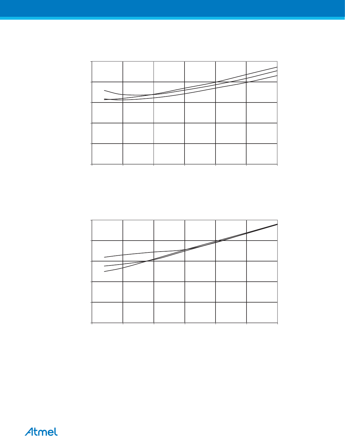
Figure 32-41 Reset Pin as I/O - Pin Hysteresis vs. VCC
RESET P IN AS IO, PIN HYSTERES IS vs. V
CC
85 °C
25 °C
-40 °C
0
0.1
0.2
0.3
0.4
0.5
2.5 3 3.5 4 4.5 5 5.5
VCC (V)
Input Hys tere s is (mV)
Figure 32-42 Reset Input Threshold Voltage vs. VCC (VIH, Reset Pin Read as “1”)
RESET INP UT THRESHOLD VOLTAGE vs . V
CC
VIH, RES ET PIN READ AS '1'
85 °C
25 °C
-40 °C
0
0.5
1
1.5
2
2.5
2.5 3 3.5 4 4.5 5 5.5
VCC (V)
Thres hold (V)
Atmel ATmega8A [DATASHEET]
Atmel-8159F-8-bit AVR Microcontroller_Datasheet_Complete-09/2015
335
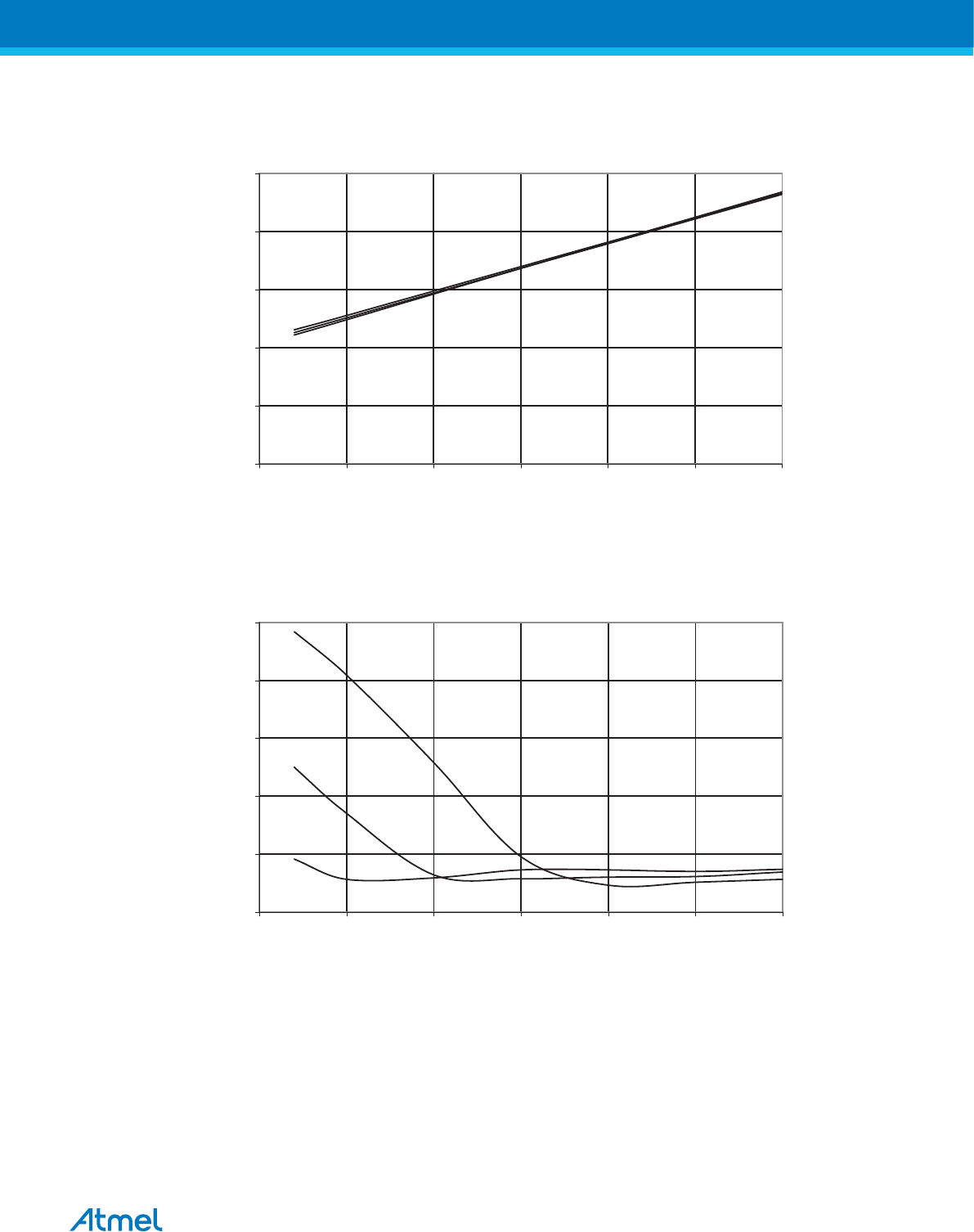
Figure 32-43 Reset Input Threshold Voltage vs. VCC (VIL, Reset Pin Read as “0”)
RESET INP UT THRESHOLD VOLTAGE vs . VCC
VIL, RES ET PIN READ AS '0'
85 °C
25 °C
-40 °C
0
0.5
1
1.5
2
2.5
2.5 3 3.5 4 4.5 5 5.5
VCC (V)
Thres hold (V)
Figure 32-44 Reset Input Pin Hysteresis vs. VCC
RESET INP UT PIN HYSTERES IS vs. VCC
85 °C
25 °C
-40 °C
0
0.1
0.2
0.3
0.4
0.5
2.5 3 3.5 4 4.5 5 5.5
VCC (V)
Input Hys tere s is (mV)
Atmel ATmega8A [DATASHEET]
Atmel-8159F-8-bit AVR Microcontroller_Datasheet_Complete-09/2015
336
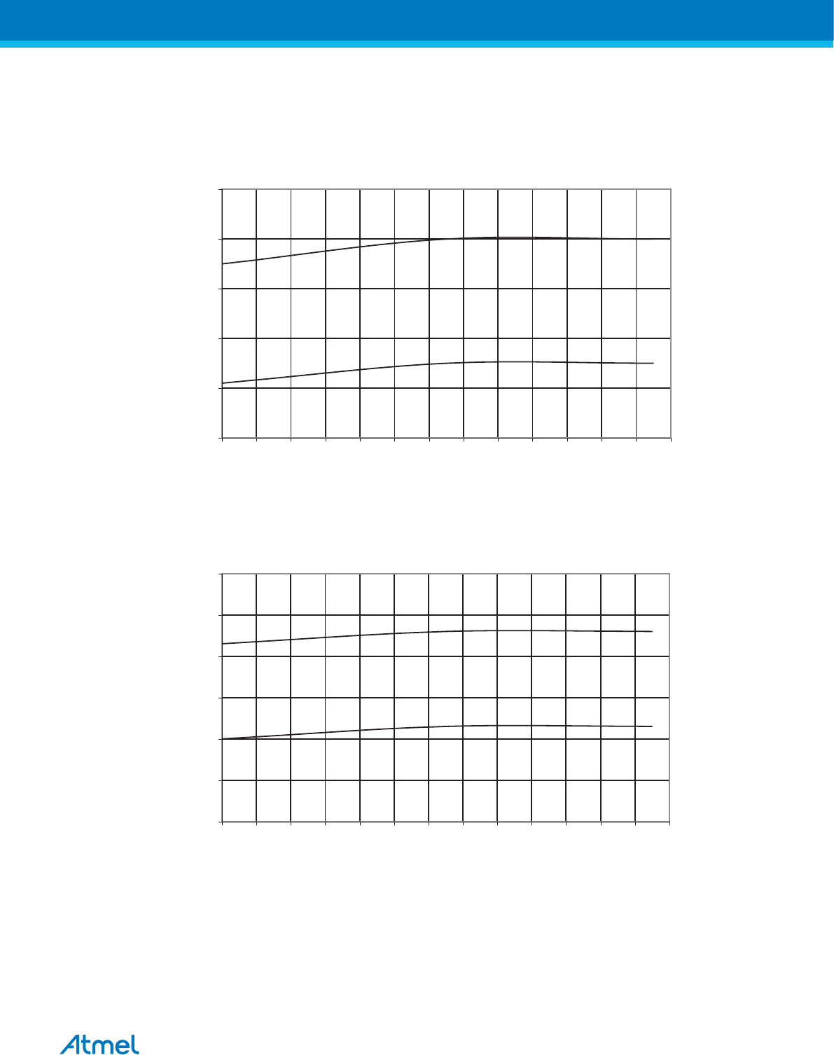
32.9. Bod Thresholds and Analog Comparator Offset
Figure 32-45 BOD Thresholds vs. Temperature (BOD Level is 4.0V)
BOD THRESHOLDS vs. TEMP ERATURE
BOD LEVEL IS 4.0V
3.7
3.75
3.8
3.85
3.9
3.95
-40 -30 -20 -10 0 10 20 30 40 50 60 70 80 90
Thres hold (V)
Rising Vcc
Fa lling Vcc
Tempera ture (
°C
)
Figure 32-46 BOD Thresholds vs. Temperature (BOD Level is 2.7v)
BOD THRESHOLDS vs. TEMP ERATURE
BOD LEVEL IS 2.7V
2.5
2.55
2.6
2.65
2.7
2.75
2.8
-40 -30 -20 -10 0 10 20 30 40 50 60 70 80 90
Tempera ture (
°C
)
Thres hold (V)
Rising Vcc
Fa lling Vcc
Atmel ATmega8A [DATASHEET]
Atmel-8159F-8-bit AVR Microcontroller_Datasheet_Complete-09/2015
337
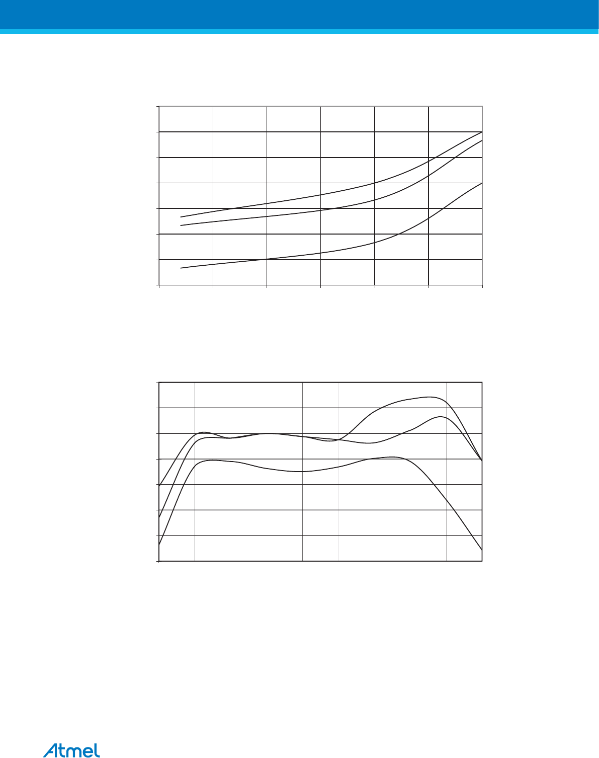
Figure 32-47 Bandgap Voltage vs. VCC
BANDGAP VOLTAGE vs . V
CC
85 °C
25 °C
-40 °C
1.18
1.185
1.19
1.195
1.2
1.205
1.21
1.215
2.5 3 3.5 4 4.5 5 5.5
Vcc (V)
Bandgap Voltage (V)
Figure 32-48 Analog Comparator Offset Voltage vs. Common Mode Voltage (VCC = 5V)
Compa ra tor Offse t Voltage (V)
0.5 1 1.5 2 2.5 3 3.5 4 4.5 5
Common Mode Voltage (V)
ANALOG COMPARATOR OFFS ET VOLTAGE vs. COMMON MODE VOLTAGE
VCC = 5V
85 °C
25 °C
-40 °C
-0.004
-0.003
-0.002
-0.001
0
0.001
0.002
0.003
Atmel ATmega8A [DATASHEET]
Atmel-8159F-8-bit AVR Microcontroller_Datasheet_Complete-09/2015
338
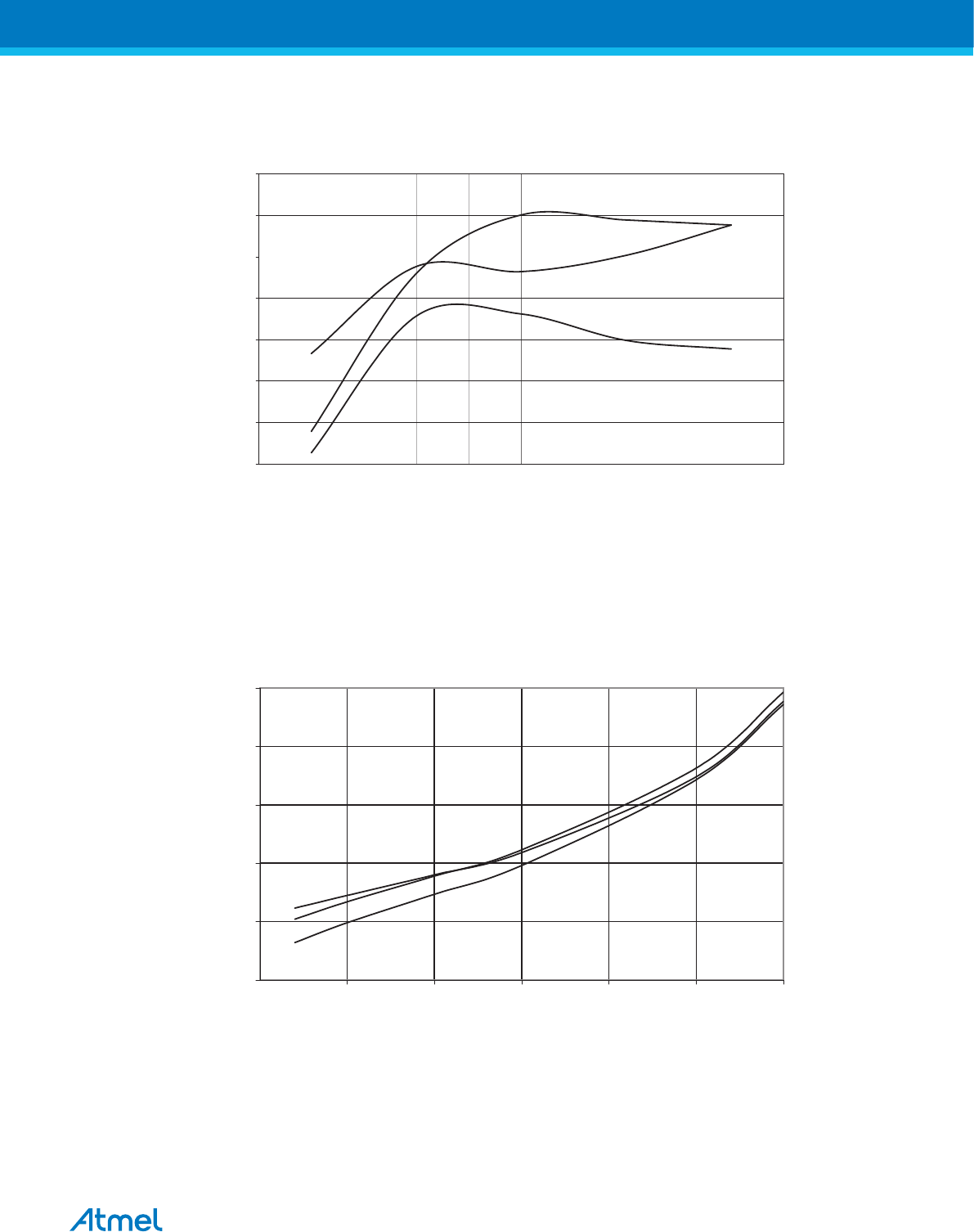
Figure 32-49 Analog Comparator Offset Voltage vs. Common Mode Voltage (VCC = 2.8V)
-0.004
-0.003
-0.002
-0.001
0
0.001
0.002
0.003
0.25 0.50 0.75 1.00 1.25 1.5 1.75 2.00 2.25 2.75
Common Mode Voltage (V)
2.50
Compa ra tor Offse t Voltage (V)
ANALOG COMPARATOR OFFS ET VOLTAGE vs. COMMON MODE VOLTAGE
V = 2.8V
CC
85 °C
25 °C
-40 °C
32.10. Internal Oscillator Speed
Figure 32-50 Watchdog Oscillator Frequency vs. VCC
WATCHDOG OSCILLATOR FREQUENCY vs . V
CC
85 °C
25 °C
-40 °C
925
950
975
1000
1025
1050
2.5 3 3.5 4 4.5 5 5.5
VCC (V)
FRC (kHz)
Atmel ATmega8A [DATASHEET]
Atmel-8159F-8-bit AVR Microcontroller_Datasheet_Complete-09/2015
339
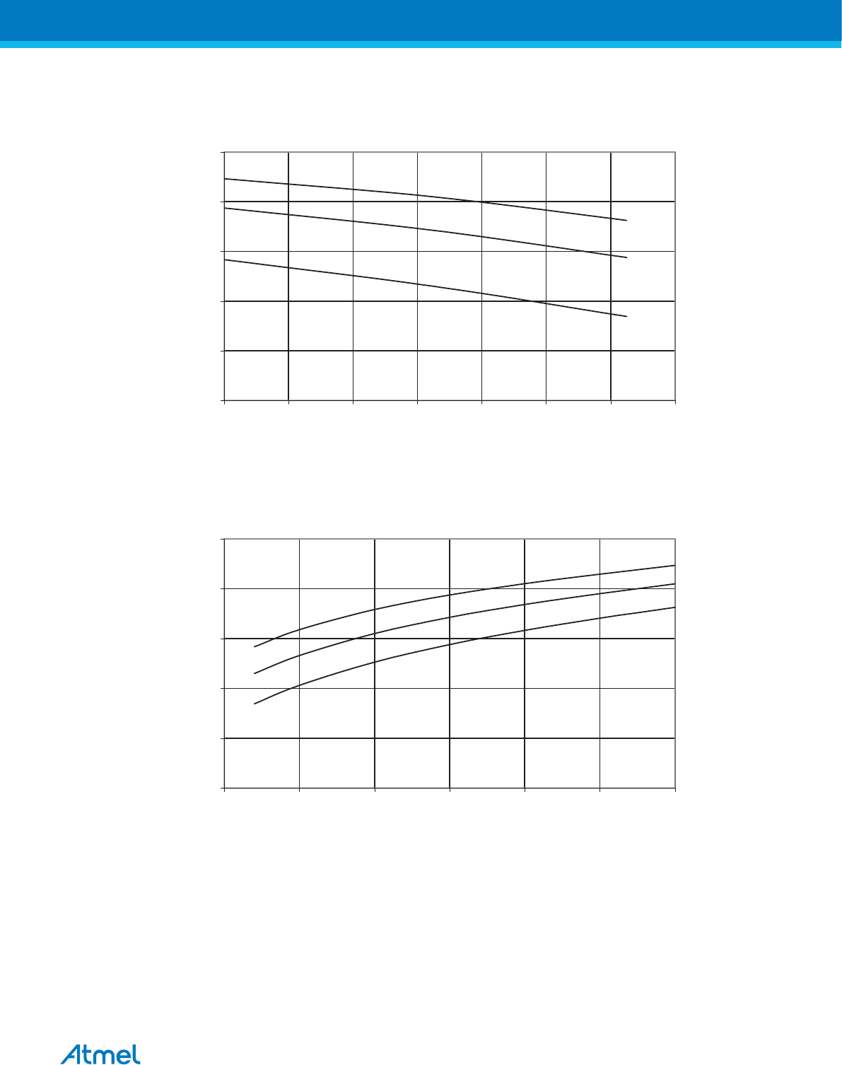
Figure 32-51 Calibrated 8MHz RC Oscillator Frequency vs. Temperature
CALIBRATED 8 MHz RC OSCILLATOR FREQUENCY vs . TEMPERATURE
5.5 V
4.0 V
2.7 V
6
6,5
7
7,5
8
8,5
-40 -20 0 20 40 60 80 100
Tempera ture (
°C)
FRC (MHz)
Figure 32-52 Calibrated 8MHz RC Oscillator Frequency vs. VCC
CALIBRATED 8 MHz RC OSCILLATOR FREQUENCY vs . V
CC
85 °C
25 °C
-40 °C
6
6.5
7
7.5
8
8.5
2.5 3 3.5 4 4.5 5 5.5
VCC (V)
FRC (MHz)
Atmel ATmega8A [DATASHEET]
Atmel-8159F-8-bit AVR Microcontroller_Datasheet_Complete-09/2015
340
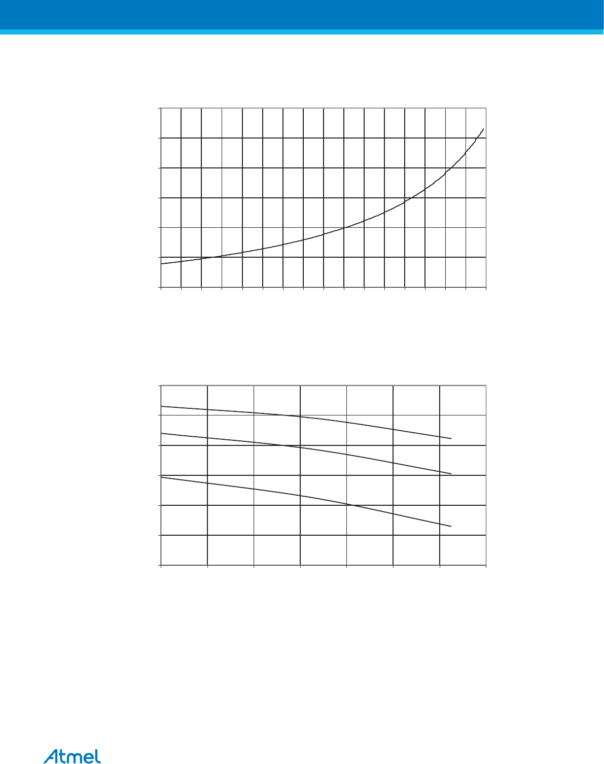
Figure 32-53 Calibrated 8MHz RC Oscillator Frequency vs. Osccal Value
CALIBRATED 8 MHz RC OSCILLATOR FREQUENCY vs . OS CCAL VALUE
25 °C
2
4
6
8
10
12
14
0 16 32 48 64 80 96 112 128 144 160 176 192 208 224 240 256
OS CCAL VALUE
FRC (MHz)
Figure 32-54 Calibrated 4MHz RC Oscillator Frequency vs. Temperature
CALIBRATED 4 MHz RC OSCILLATOR FREQUENCY vs . TEMPERATURE
5.5 V
4.0 V
2.7 V
3.5
3.6
3.7
3.8
3.9
4
4.1
-40 -20 0 20 40 60 80 100
FRC (MHz)
Tempera ture (
°C)
Atmel ATmega8A [DATASHEET]
Atmel-8159F-8-bit AVR Microcontroller_Datasheet_Complete-09/2015
341
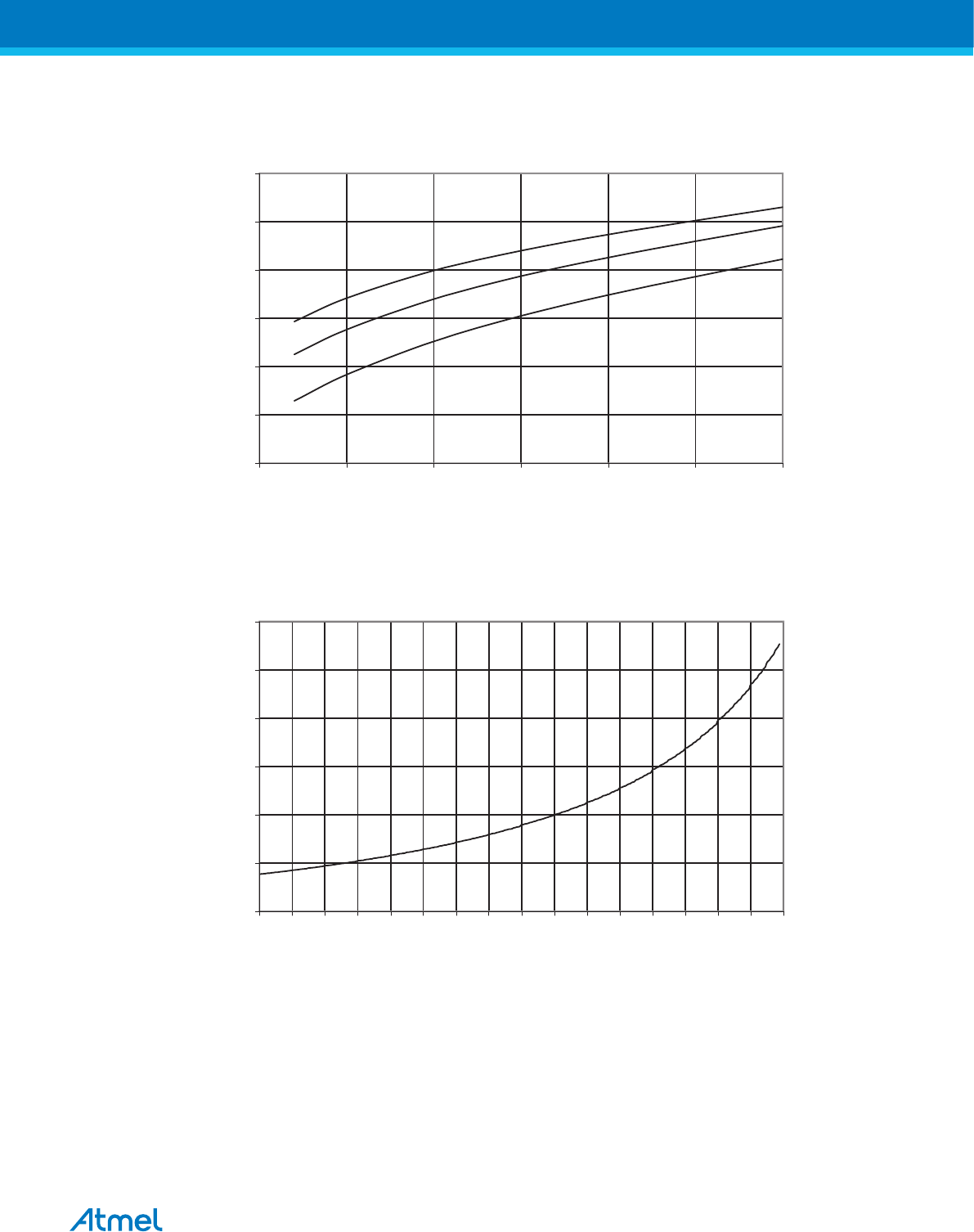
Figure 32-55 Calibrated 4MHz RC Oscillator Frequency vs. VCC
CALIBRATED 4 MHz RC OSCILLATOR FREQUENCY vs . V
CC
85 °C
25 °C
-40 °C
3.5
3.6
3.7
3.8
3.9
4
4.1
2.5 3 3.5 4 4.5 5 5.5
VCC (V)
FRC (MHz)
Figure 32-56 Calibrated 4MHz RC Oscillator Frequency vs. Osccal Value
CALIBRATED 4 MHz RC OSCILLATOR FREQUENCY vs . OS CCAL VALUE
25 °C
1
2
3
4
5
6
7
0 16 32 48 64 80 96 112 128 144 160 176 192 208 224 240 256
OS CCAL VALUE
FRC (MHz)
Atmel ATmega8A [DATASHEET]
Atmel-8159F-8-bit AVR Microcontroller_Datasheet_Complete-09/2015
342
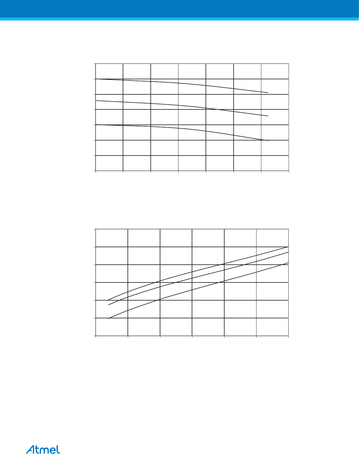
Figure 32-57 Calibrated 2MHz RC Oscillator Frequency vs. Temperature
CALIBRATED 2 MHz RC OSCILLATOR FREQUENCY vs . TEMPERATURE
5.5 V
4.0 V
2.7 V
1.75
1.8
1.85
1.9
1.95
2
2.05
2.1
-40 -20 0 20 40 60 80 100
FRC (MHz)
Tempera ture (
°C)
Figure 32-58 Calibrated 2MHz RC Oscillator Frequency vs. VCC
CALIBRATED 2 MHz RC OSCILLATOR FREQUENCY vs . V
CC
85 °C
25 °C
-40 °C
1.8
1.85
1.9
1.95
2
2.05
2.1
2.5 3 3.5 4 4.5 5 5.5
VCC (V)
FRC (MHz)
Atmel ATmega8A [DATASHEET]
Atmel-8159F-8-bit AVR Microcontroller_Datasheet_Complete-09/2015
343
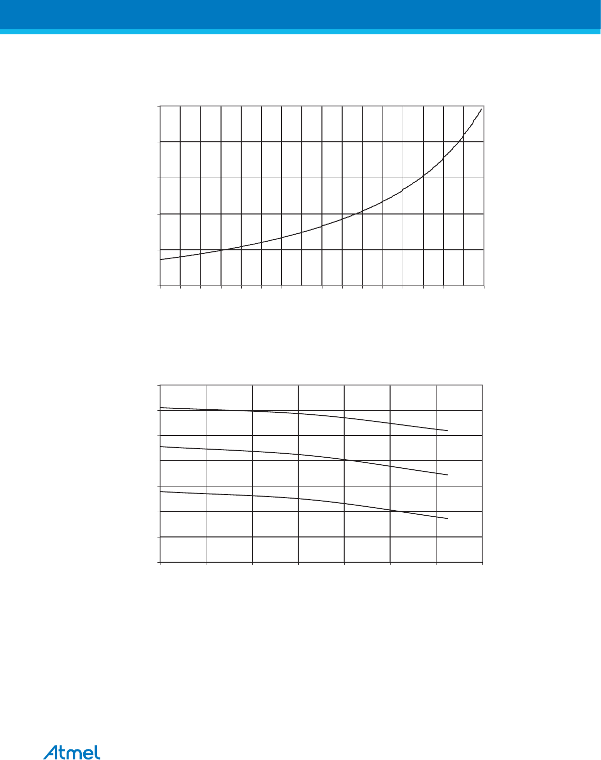
Figure 32-59 Calibrated 2MHz RC Oscillator Frequency vs. Osccal Value
CALIBRATED 2 MHz RC OSCILLATOR FREQUENCY vs . OS CCAL VALUE
25 °C
0.5
1
1.5
2
2.5
3
0 16 32 48 64 80 96 112 128 144 160 176 192 208 224 240 256
OS CCAL VALUE
FRC (MHz)
Figure 32-60 Calibrated 1MHz RC Oscillator Frequency vs. Temperature
CALIBRATED 1 MHz RC OSCILLATOR FREQUENCY vs . TEMPERATURE
5.5 V
4.0 V
2.7 V
0.9
0.92
0.94
0.96
0.98
1
1.02
1.04
-40 -20 0 20 40 60 80 100
FRC (MHz)
Tempera ture (
°C)
Atmel ATmega8A [DATASHEET]
Atmel-8159F-8-bit AVR Microcontroller_Datasheet_Complete-09/2015
344
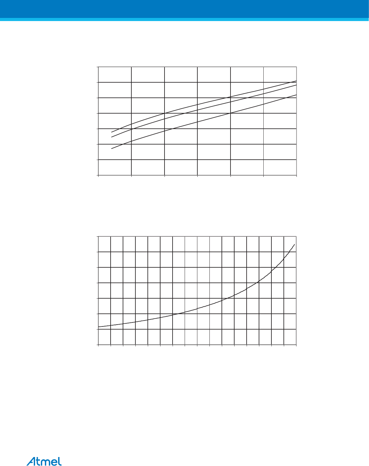
Figure 32-61 Calibrated 1MHz RC Oscillator Frequency vs. VCC
CALIBRATED 1 MHz RC OSCILLATOR FREQUENCY vs . V
CC
85 °C
25 °C
-40 °C
0,9
0.92
0.94
0.96
0.98
1
1.02
1.04
2.5 3 3.5 4 4.5 5 5.5
VCC (V)
FRC (MHz)
Figure 32-62 Calibrated 1MHz RC Oscillator Frequency vs. Osccal Value
CALIBRATED 1 MHz RC OSCILLATOR FREQUENCY vs . OS CCAL VALUE
25 °C
0.2
0.4
0.6
0.8
1
1.2
1.4
1.6
0 16 32 48 64 80 96 112 128 144 160 176 192 208 224 240 256
OS CCAL VALUE
FRC (MHz)
Atmel ATmega8A [DATASHEET]
Atmel-8159F-8-bit AVR Microcontroller_Datasheet_Complete-09/2015
345
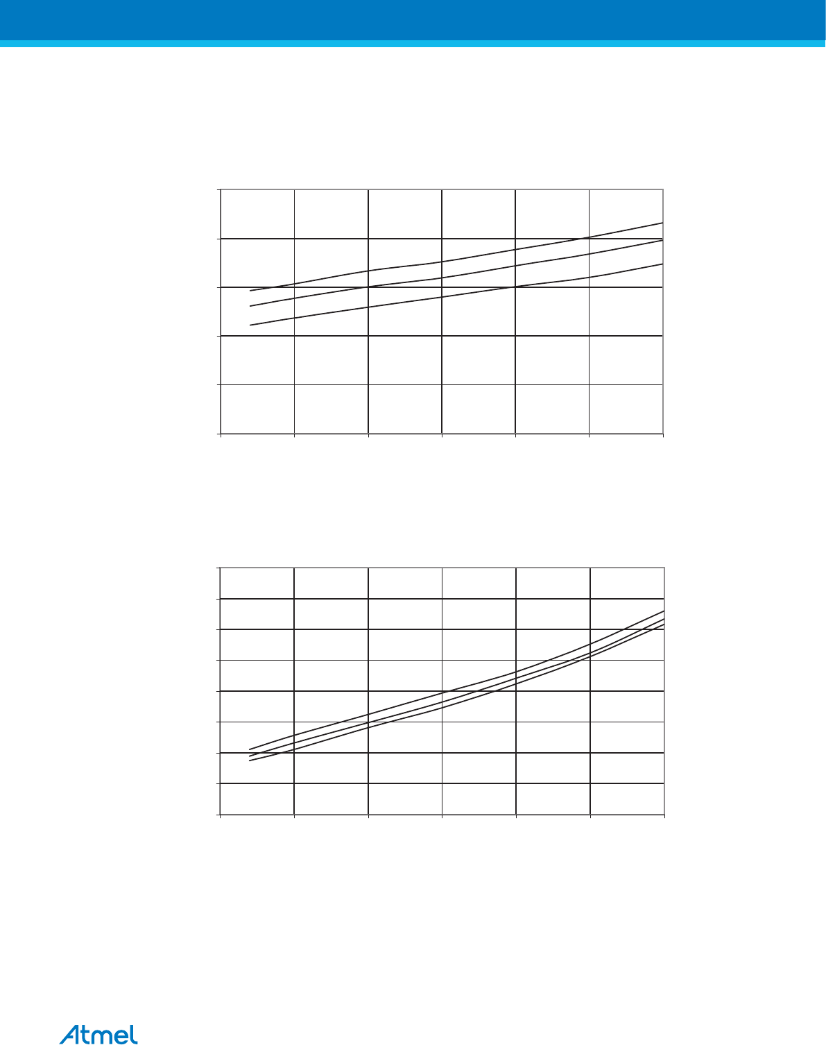
32.11. Current Consumption of Peripheral Units
Figure 32-63 Brown-out Detector Current vs. VCC
BROWN-OUT DETECTOR CURRENT vs . V
CC
85 °C
25 °C
-40 °C
0
4
8
12
16
20
2.5 3 3.5 4 4.5 5 5.5
VCC (V)
ICC (uA)
Figure 32-64 ADC Current vs. VCC (AREF = AVCC)
ADC CURRENT vs . VCC
AREF = AVCC
85 °C
25 °C
-40 °C
100
125
150
175
200
225
250
275
300
2.5 3 3.5 4 4.5 5 5.5
VCC (V)
ICC (uA)
Atmel ATmega8A [DATASHEET]
Atmel-8159F-8-bit AVR Microcontroller_Datasheet_Complete-09/2015
346
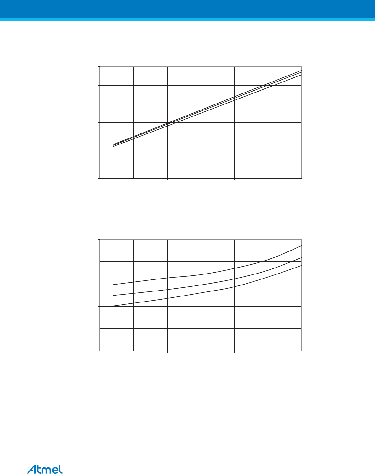
Figure 32-65 AREF External Reference Current vs. VCC
AREF EXTERNAL REFERENCE CURRENT vs . VCC
85 °C
25 °C
-40 °C
40
60
80
100
120
140
160
2.5 3 3.5 4 4.5 5 5.5
VCC (V)
ICC (uA)
Figure 32-66 32kHz TOSC Current vs. VCC (Watchdog Timer Disabled)
32 kHz TOSC CURRENT vs . VCC
WATCHDOG TIMER DISABLED
85 °C
25 °C
-40 °C
0
2
4
6
8
10
2.5 3 3.5 4 4.5 5 5.5
VCC (V)
ICC (uA)
Atmel ATmega8A [DATASHEET]
Atmel-8159F-8-bit AVR Microcontroller_Datasheet_Complete-09/2015
347
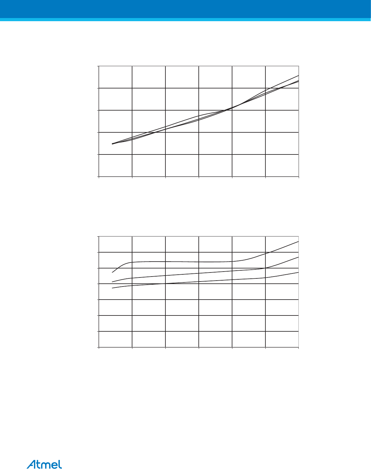
Figure 32-67 Watchdog Timer Current vs. VCC
WATCHDOG TIMER CURRENT vs . V
CC
85 °C
25 °C
-40 °C
0
4
8
12
16
20
2.5 3 3.5 4 4.5 5 5.5
VCC (V)
ICC (uA)
Figure 32-68 Analog Comparator Current vs. VCC
ANALOG COMPARATOR CURRENT vs . VCC
85 °C
25 °C
-40 °C
0
10
20
30
40
50
60
70
2.5 3 3.5 4 4.5 5 5.5
VCC (V)
ICC (uA)
Atmel ATmega8A [DATASHEET]
Atmel-8159F-8-bit AVR Microcontroller_Datasheet_Complete-09/2015
348
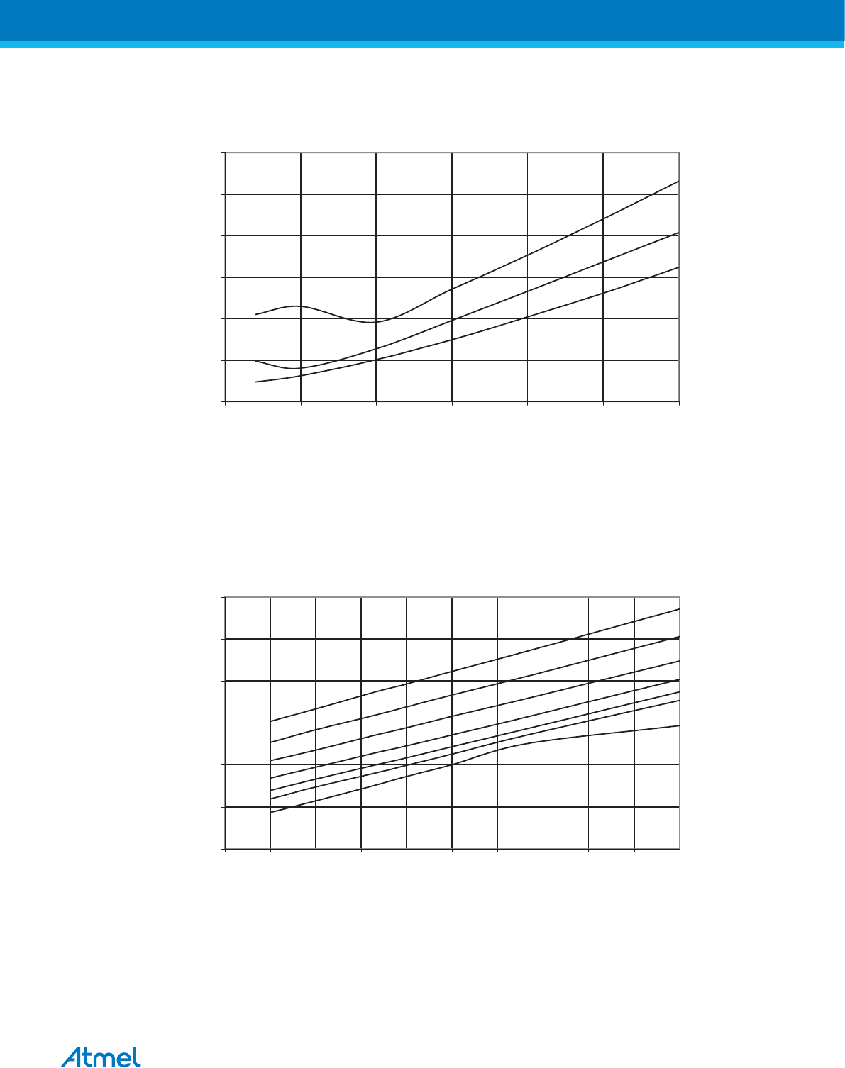
Figure 32-69 Programming Current vs. VCC
PROGRAMMING CURRENT vs. V
CC
85 °C
25 °C
-40 °C
0
1
2
3
4
5
6
2.5 3 3.5 4 4.5 5 5.5
VCC (V)
ICC (mA)
32.12. Current Consumption in Reset and Reset Pulsewidth
Figure 32-70 Reset Supply Current vs. VCC (0.1 - 1.0MHz, Excluding Current Through The Reset Pull-up)
RESET S UPPLY CURRENT vs . VCC
0.1 - 1.0 MHz EXCLUDING CURRENT THROUGH THE RESET PULLUP
5.5 V
5.0 V
4.5 V
4.0 V
3.6 V
3.3 V
2.7 V
0
0.5
1
1.5
2
2.5
3
0 0.1 0.2 0.3 0.4 0.5 0.6 0.7 0.8 0.9 1
Fre quency (MHz)
ICC (mA)
Atmel ATmega8A [DATASHEET]
Atmel-8159F-8-bit AVR Microcontroller_Datasheet_Complete-09/2015
349
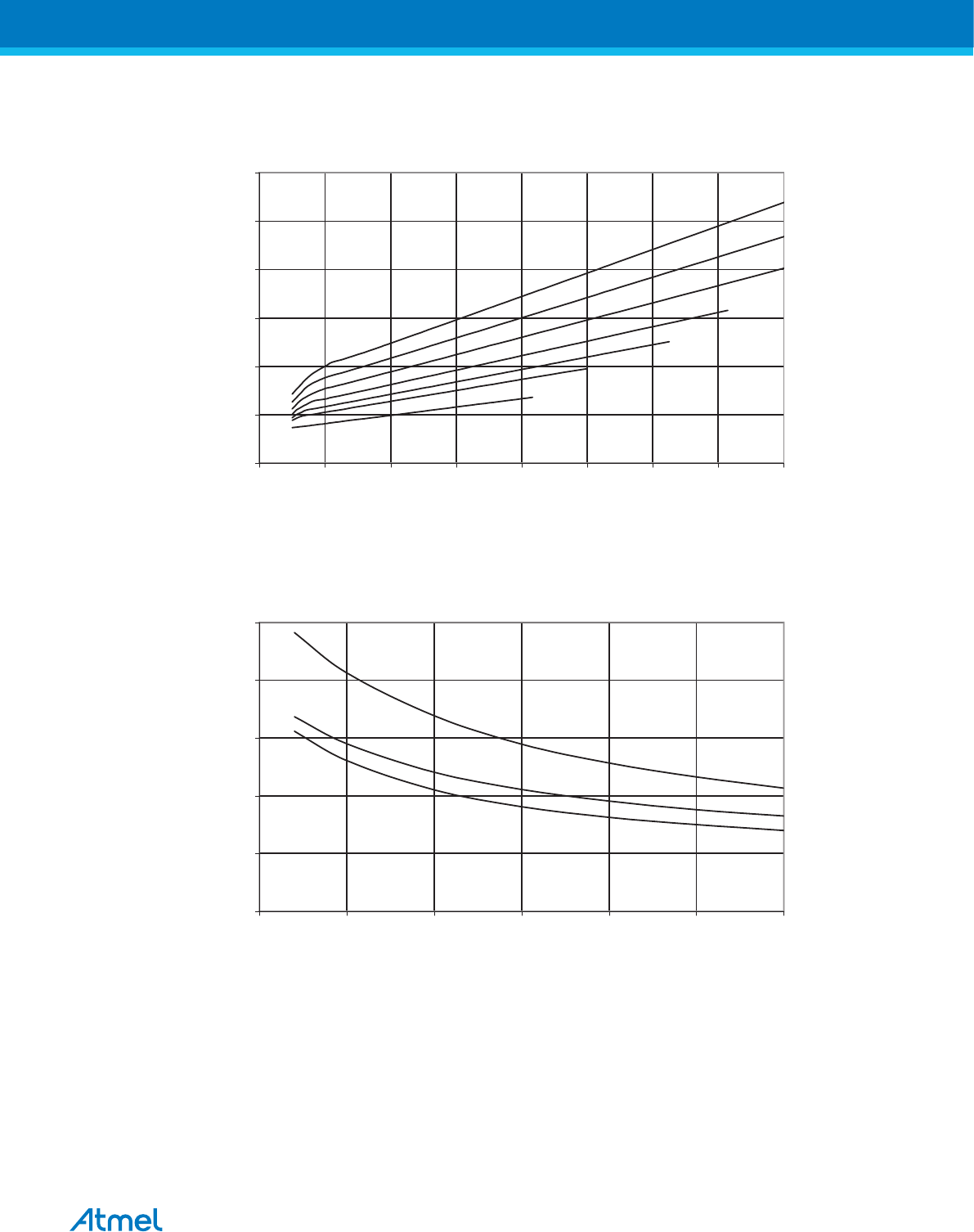
Figure 32-71 Reset Supply Current vs. VCC (1 - 16MHz, Excluding Current Through The Reset Pull-up)
5.5 V
5.0 V
4.5 V
4.0 V
3.6 V
3.3 V
2.7 V
RESET S UPPLY CURRENT vs . VCC
1 - 16 MHz EXCLUDING CURRENT THROUGH THE RES ET P ULLUP
0
2
4
6
8
10
12
0 2 4 6 8 10 12 14 16
Fre quency (MHz)
ICC (mA)
Figure 32-72 Reset Pulse Width vs. VCC
MINIMUM RESET PULSE WIDTH vs. V
CC
85 °C
25 °C
-40 °C
0
150
300
450
600
750
2,5 3 3,5 4 4,5 5 5,5
VCC (V)
Pulsewidth (ns)
Atmel ATmega8A [DATASHEET]
Atmel-8159F-8-bit AVR Microcontroller_Datasheet_Complete-09/2015
350

33. Typical Characteristics – TA = -40°C to 105°C
The following charts show typical behavior. These figures are not tested during manufacturing. All current
consumption measurements are performed with all I/O pins configured as inputs and with internal pull-ups
enabled. A sine wave generator with rail-to-rail output is used as clock source.
All Active- and Idle current consumption measurements are done with all bits in the PRR registers set and
thus, the corresponding I/O modules are turned off. Also the Analog Comparator is disabled during these
measurements. The power consumption in Power-down mode is independent of clock selection.
The current consumption is a function of several factors such as: operating voltage, operating frequency,
loading of I/O pins, switching rate of I/O pins, code executed and ambient temperature. The dominating
factors are operating voltage and frequency.
The current drawn from capacitive loaded pins may be estimated (for one pin) as CL*VCC*f where CL =
load capacitance, VCC = operating voltage and f = average switching frequency of I/O pin.
The parts are characterized at frequencies higher than test limits. Parts are not guaranteed to function
properly at frequencies higher than the ordering code indicates.
The difference between current consumption in Power-down mode with Watchdog Timer enabled and
Power-down mode with Watchdog Timer disabled represents the differential current drawn by the
Watchdog Timer.
33.1. ATmega8A Typical Characteristics
33.1.1. Active Supply Current
Figure 33-1 Active Supply Current vs. VCC (Internal RC Oscillator, 8 MHz)
ACTIVE S UP P LY CURRENT vs. VCC
INTERNAL RC OS CILLATOR, 8 MHz
105 °C
85 °C
25 °C
-40 °C
2.5
3.5
4.5
5.5
6.5
7.5
8.5
9.5
2.5 2.8 3.1 3.4 3.7 4 4.3 4.6 4.9 5.2 5.5
VCC (V)
ICC (mA)
Atmel ATmega8A [DATASHEET]
Atmel-8159F-8-bit AVR Microcontroller_Datasheet_Complete-09/2015
351
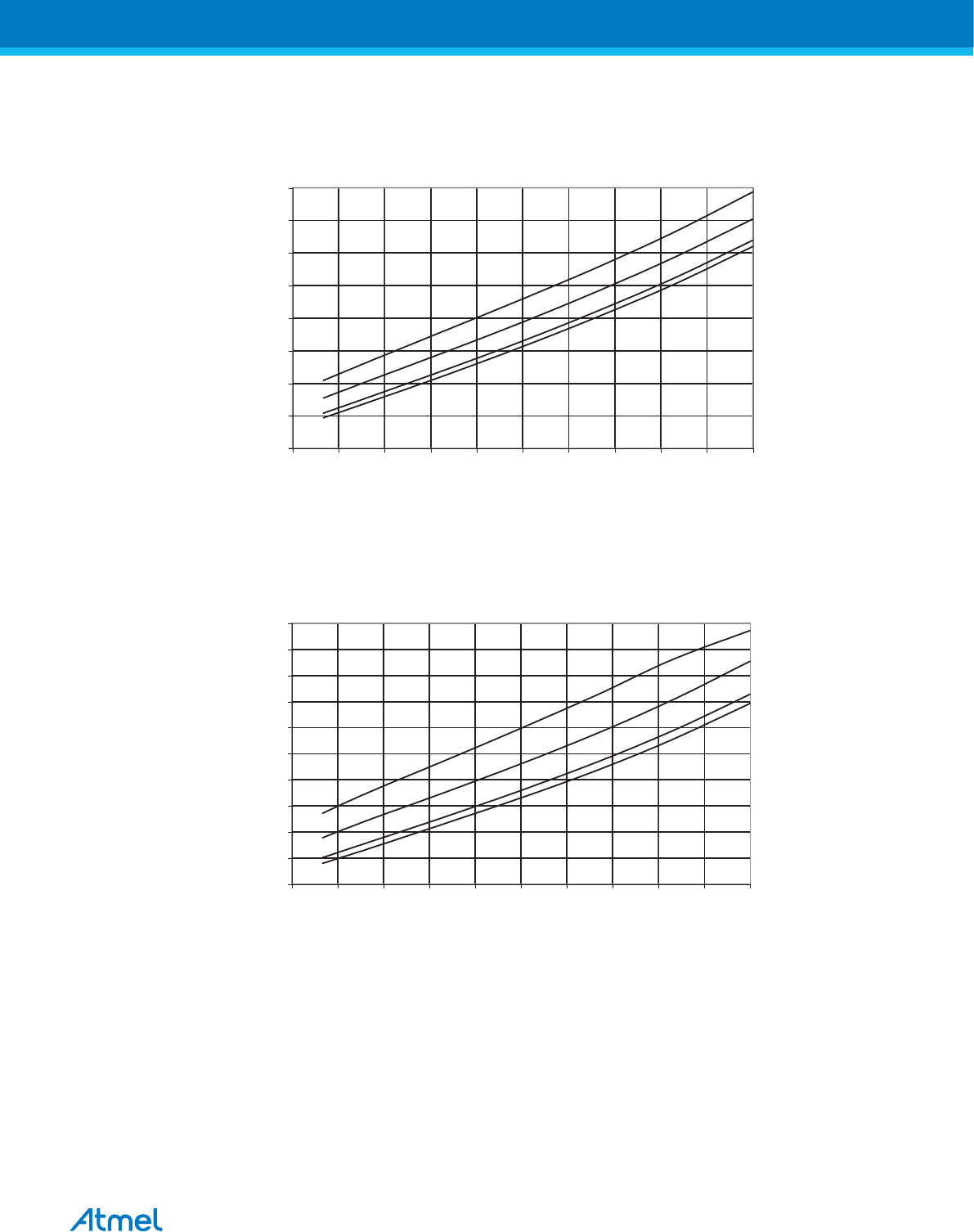
Figure 33-2 Active Supply Current vs. VCC (Internal RC Oscillator, 4 MHz)
ACTIVE S UP P LY CURRENT vs. VCC
INTERNAL RC OS CILLATOR, 4 MHz
105 °C
85 °C
25 °C
-40 °C
1.5
2
2.5
3
3.5
4
4.5
5
5.5
2.5 2.8 3.1 3.4 3.7 4 4.3 4.6 4.9 5.2 5.5
VCC (V)
ICC (mA)
Figure 33-3 Active Supply Current vs. VCC (Internal RC Oscillator, 2 MHz)
ACTIVE S UP P LY CURRENT vs. VCC
INTERNAL RC OS CILLATOR, 2 MHz
105 °C
85 °C
25 °C
-40 °C
1
1.25
1.5
1.75
2
2.25
2.5
2.75
3
3.25
3.5
2.5 2.8 3.1 3.4 3.7 4 4.3 4.6 4.9 5.2 5.5
VCC (V)
ICC (mA)
Atmel ATmega8A [DATASHEET]
Atmel-8159F-8-bit AVR Microcontroller_Datasheet_Complete-09/2015
352
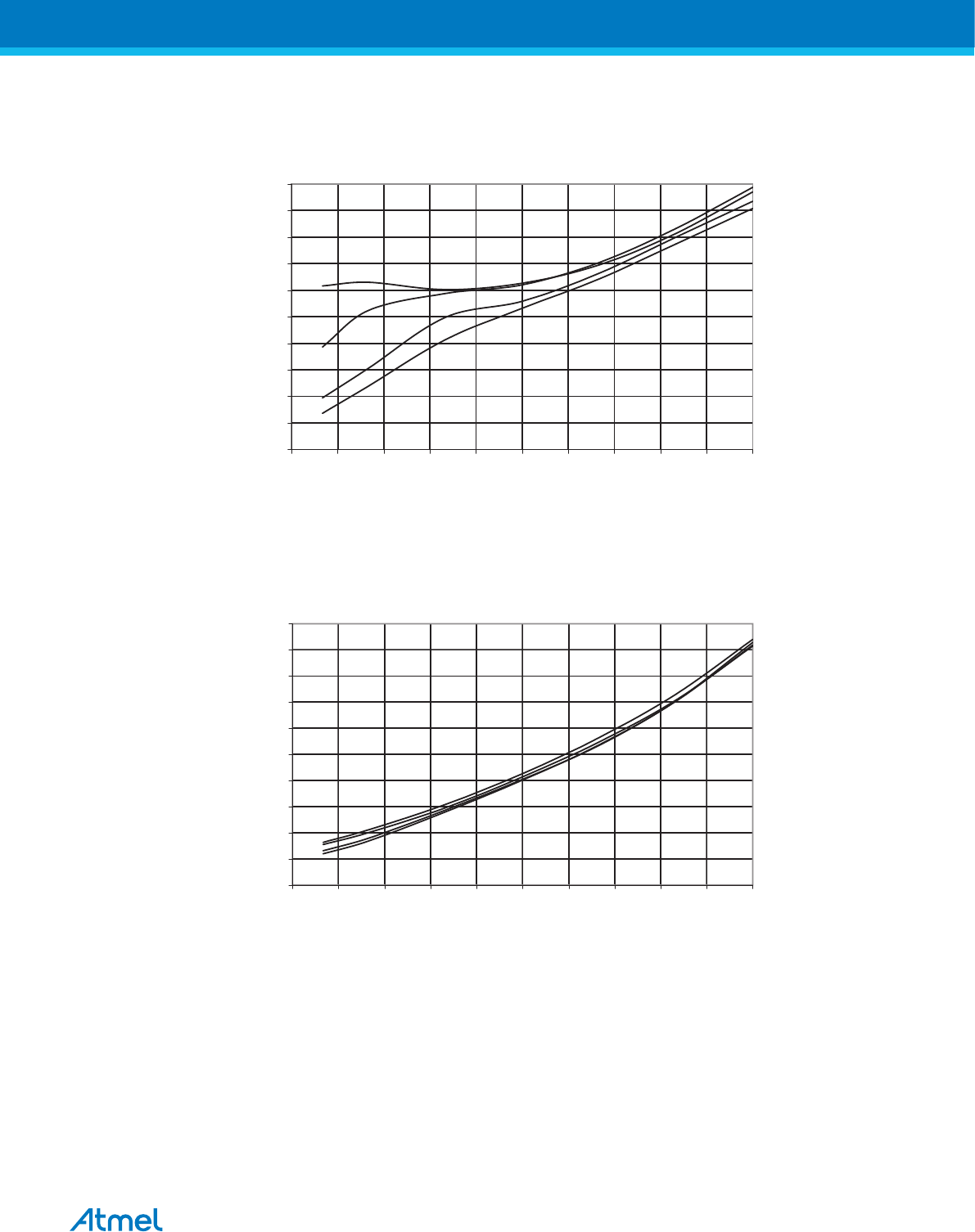
Figure 33-4 Active Supply Current vs. VCC (Internal RC Oscillator, 1 MHz)
ACTIVE S UP P LY CURRENT vs. VCC
INTERNAL RC OS CILLATOR, 1 MHz
105 °C
85 °C
25 °C
-40 °C
0.8
0.9
1
1.1
1.2
1.3
1.4
1.5
1.6
1.7
1.8
2.5 2.8 3.1 3.4 3.7 4 4.3 4.6 4.9 5.2 5.5
VCC (V)
ICC (mA)
Figure 33-5 Active Supply Current vs. VCC (32 kHz External Oscillator)
ICC ACTIVE S UP P LY CURRENT vs . VCC
32 kHz Crystal Os cilla tor WDT DIS ABLED
105 °C
85 °C
25 °C
-40 °C
35
38
41
44
47
50
53
56
59
62
65
2.5 2.8 3.1 3.4 3.7 4 4.3 4.6 4.9 5.2 5.5
VCC (V)
I
CC
(uA)
Atmel ATmega8A [DATASHEET]
Atmel-8159F-8-bit AVR Microcontroller_Datasheet_Complete-09/2015
353
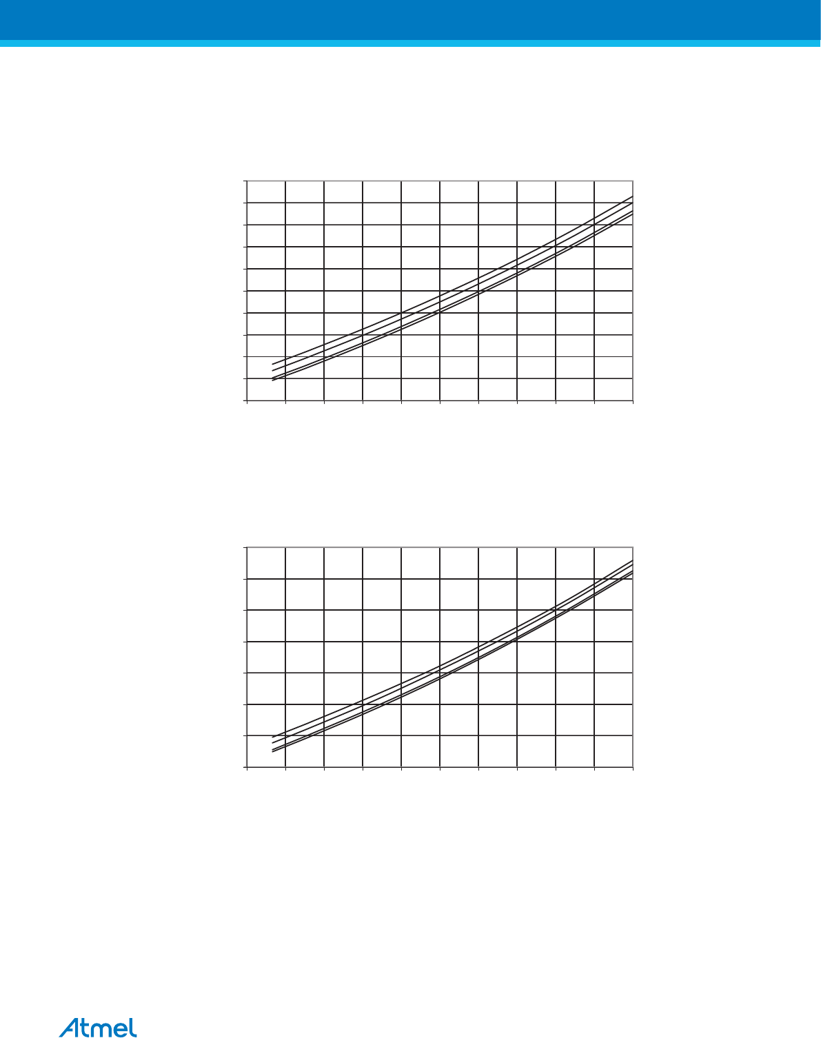
33.1.2. Idle Supply Current
Figure 33-6 Idle Supply Current vs. VCC (Internal RC Oscillator, 8MHz)
IDLE S UP P LY CURRENT vs. VCC
INTERNAL RC OS CILLATOR, 8 MHz
105 °C
85 °C
25 °C
-40 °C
1.2
1.5
1.8
2.1
2.4
2.7
3
3.3
3.6
3.9
4.2
2.5 2.8 3.1 3.4 3.7 4 4.3 4.6 4.9 5.2 5.5
VCC (V)
ICC (mA)
Figure 33-7 Idle Supply Current vs. VCC (Internal RC Oscillator, 4MHz)
IDLE S UP P LY CURRENT vs. VCC
INTERNAL RC OS CILLATOR, 4 MHz
105 °C
85 °C
25 °C
-40 °C
0.7
0.9
1.1
1.3
1.5
1.7
1.9
2.1
2.5 2.8 3.1 3.4 3.7 4 4.3 4.6 4.9 5.2 5.5
VCC (V)
ICC (mA)
Atmel ATmega8A [DATASHEET]
Atmel-8159F-8-bit AVR Microcontroller_Datasheet_Complete-09/2015
354
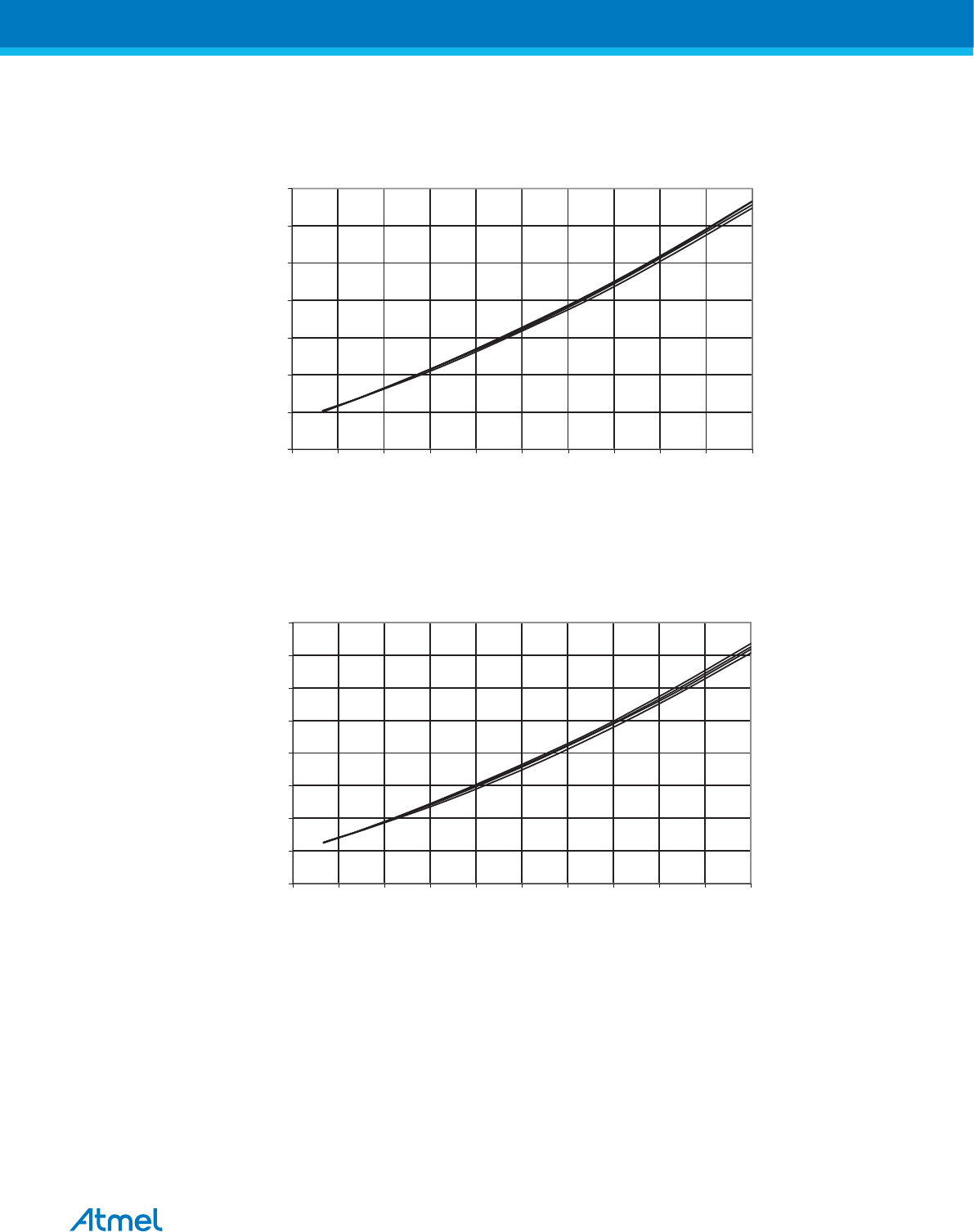
Figure 33-8 Idle Supply Current vs. VCC (Internal RC Oscillator, 2MHz)
IDLE S UP P LY CURRENT vs. VCC
INTERNAL RC OS CILLATOR, 2 MHz
105 °C
85 °C
25 °C
-40 °C
0.2
0.3
0.4
0.5
0.6
0.7
0.8
0.9
2.5 2.8 3.1 3.4 3.7 4 4.3 4.6 4.9 5.2 5.5
VCC (V)
ICC (mA)
Figure 33-9 Idle Supply Current vs. VCC (Internal RC Oscillator, 1MHz)
IDLE S UP P LY CURRENT vs. VCC
INTERNAL RC OS CILLATOR, 1 MHz
105 °C
85 °C
25 °C
-40 °C
0.1
0.15
0.2
0.25
0.3
0.35
0.4
0.45
0.5
2.5 2.8 3.1 3.4 3.7 4 4.3 4.6 4.9 5.2 5.5
VCC (V)
ICC (mA)
Atmel ATmega8A [DATASHEET]
Atmel-8159F-8-bit AVR Microcontroller_Datasheet_Complete-09/2015
355
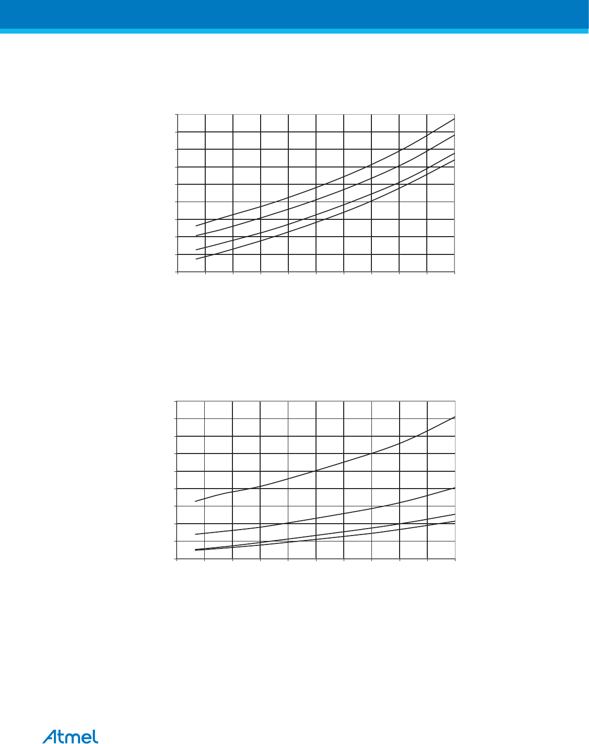
Figure 33-10 Idle Supply Current vs. VCC (32kHz External RC Oscillator)
POWER-S AVE SUP P LY CURRENT vs. VCC
WATCHDOG TIMER DISABLED
105 °C
85 °C
25 °C
-40 °C
6.5
8.5
10.5
12.5
14.5
16.5
18.5
20.5
22.5
24.5
2.5 2.8 3.1 3.4 3.7 4 4.3 4.6 4.9 5.2 5.5
VCC (V)
ICC (uA)
33.1.3. Power-down Supply Current
Figure 33-11 Power-down Supply Current vs. VCC (Watchdog Timer Disabled)
POWER-DOWN S UP P LY CURRENT vs . VCC
WATCHDOG TIMER DISABLED
105 °C
85 °C
25 °C
-40 °C
0
0.5
1
1.5
2
2.5
3
3.5
4
4.5
2.5 2.8 3.1 3.4 3.7 4 4.3 4.6 4.9 5.2 5.5
VCC (V)
ICC (uA)
Atmel ATmega8A [DATASHEET]
Atmel-8159F-8-bit AVR Microcontroller_Datasheet_Complete-09/2015
356
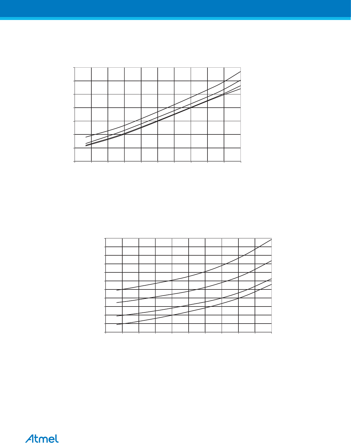
Power-down Supply Current vs. VCC (Watchdog Timer Enabled)
POWER-DOWN S UP P LY CURRENT vs. VCC
WATCHDOG TIMER ENABLED
105 °C
85 °C
25 °C
-40 °C
3
6
9
12
15
18
21
24
2.5 2.8 3.1 3.4 3.7 4 4.3 4.6 4.9 5.2 5.5
VCC (V)
ICC (uA)
33.1.4. Power-save Supply Current
Figure 33-12 Power-save Supply Current vs. VCC (Watchdog Timer Disabled)
POWER-S AVE SUP P LY CURRENT vs . VCC
WATCHDOG TIMER DISABLED
105 °C
85 °C
25 °C
-40 °C
4
5
6
7
8
9
10
11
12
13
14
15
2.5 2.8 3.1 3.4 3.7 4 4.3 4.6 4.9 5.2 5.5
VCC (V)
ICC (uA)
Atmel ATmega8A [DATASHEET]
Atmel-8159F-8-bit AVR Microcontroller_Datasheet_Complete-09/2015
357
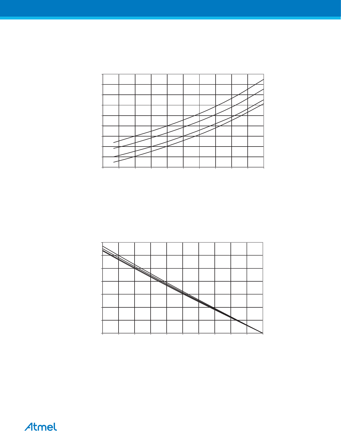
33.1.5. Standby Supply Current
Figure 33-13 Standby Supply Current vs. VCC (32kHz External RC Oscillator)
STANDBY CURRENT vs . VCC
32 kHz Crystal Oscillator WDT DIS ABLED
105 °C
85 °C
25 °C
-40 °C
7
9
11
13
15
17
19
21
23
25
2.5 2.8 3.1 3.4 3.7 4 4.3 4.6 4.9 5.2 5.5
VCC (V)
I
CC
(uA)
33.1.6. Pin Pull-up
Figure 33-14 I/O Pin Pull-up Resistor Current vs. Input Voltage (VCC = 5V)
I/O PIN PULL-UP RESISTOR CURRENT vs . INPUT VOLTAGE
0
20
40
60
80
100
120
140
0 0.5 1 1.5 2 2.5 3 3.5 4 4.5 5
VOP (V)
IOP (uA)
105 °C
85 °C
25 °C
-40 °C
Atmel ATmega8A [DATASHEET]
Atmel-8159F-8-bit AVR Microcontroller_Datasheet_Complete-09/2015
358
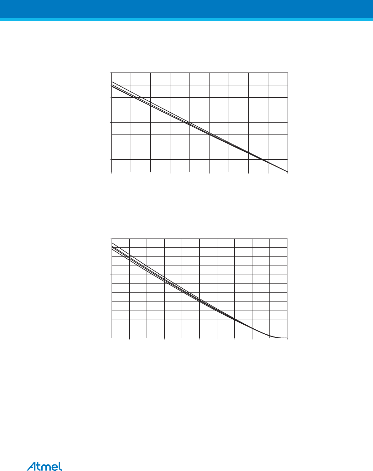
Figure 33-15 I/O Pin Pull-up Resistor Current vs. Input Voltage (VCC = 2.7V)
I/O PIN PULL-UP RESISTOR CURRENT vs . INPUT VOLTAGE
105 °C
85 °C
25 °C
-40 °C
0
10
20
30
40
50
60
70
80
0 0.3 0.6 0.9 1.2 1.5 1.8 2.1 2.4 2.7
VOP (V)
IOP (uA)
Figure 33-16 Reset Pull-up Resistor Current vs. Reset Pin Voltage (VCC = 5V)
RESET P ULL-UP RESISTOR CURRENT vs . RESET P IN VOLTAGE
0
10
20
30
40
50
60
70
80
90
100
110
0 0.5 1 1.5 2 2.5 3 3.5 4 4.5 5
VRES ET (V)
IRES ET (uA)
105 °C
85 °C
25 °C
-40 °C
Atmel ATmega8A [DATASHEET]
Atmel-8159F-8-bit AVR Microcontroller_Datasheet_Complete-09/2015
359
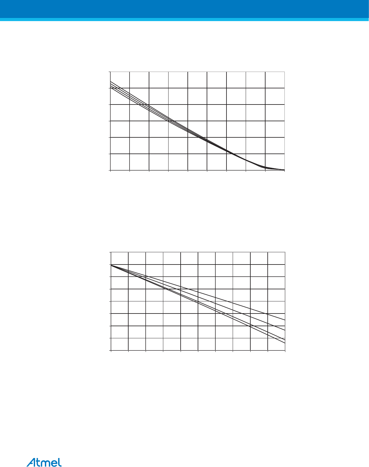
Figure 33-17 Reset Pull-up Resistor Current vs. Reset Pin Voltage (VCC = 2.7V)
RESET P ULL-UP RES ISTOR CURRENT vs . RESET P IN VOLTAGE
105 °C
85 °C
25 °C
-40 °C
0
10
20
30
40
50
60
0 0.3 0.6 0.9 1.2 1.5 1.8 2.1 2.4 2.7
VRES ET (V)
IRES ET (uA)
33.1.7. Pin Driver Strength
Figure 33-18 I/O Pin Output Voltage vs. Source Current (VCC = 5V)
105 °C
85 °C
25 °C
-40 °C
I/O PIN OUTP UT VOLTAGE vs . SOURCE CURRENT
NORMAL P OWER P INS
4.3
4.4
4.5
4.6
4.7
4.8
4.9
5
5.1
0 2 4 6 8 10 12 14 16 18 20
IOH (mA)
VOH (V)
Atmel ATmega8A [DATASHEET]
Atmel-8159F-8-bit AVR Microcontroller_Datasheet_Complete-09/2015
360
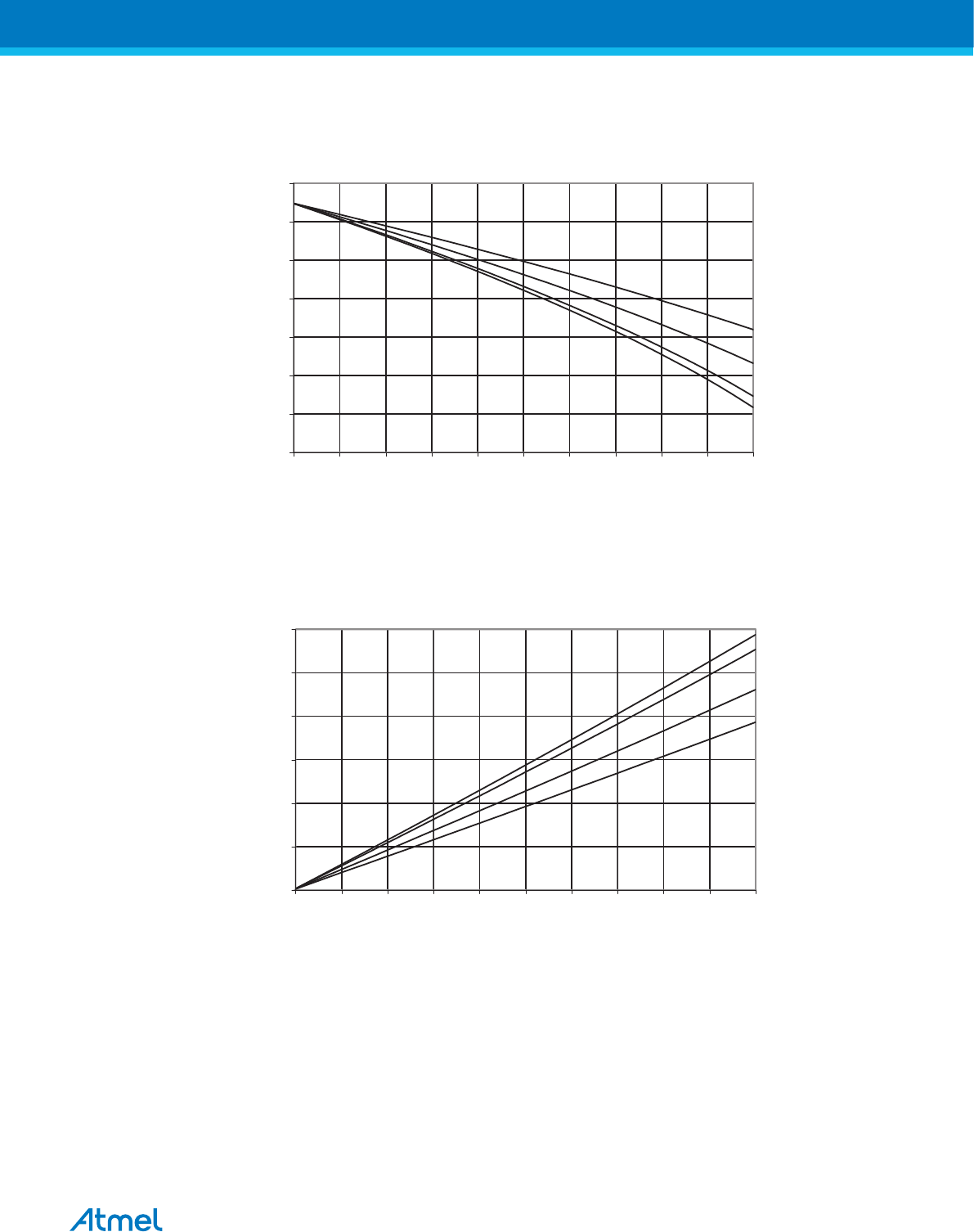
Figure 33-19 I/O Pin Output Voltage vs. Source Current (VCC = 3V)
I/O PIN OUTP UT VOLTAGE vs . SOURCE CURRENT
NORMAL P OWER P INS
1.7
1.9
2.1
2.3
2.5
2.7
2.9
3.1
0 2 4 6 8 10 12 14 16 18 20
IOH (mA)
VOH (V)
105 °C
85 °C
25 °C
-40 °C
Figure 33-20 I/O Pin Output Voltage vs. Sink Current (VCC = 5V)
105 °C
85 °C
25 °C
-40 °C
I/O PIN OUTP UT VOLTAGE vs . SINK CURRENT
NORMAL P OWER P INS
0
0.1
0.2
0.3
0.4
0.5
0.6
0 2 4 6 8 10 12 14 16 18 20
IOL (mA)
VOL (V)
Atmel ATmega8A [DATASHEET]
Atmel-8159F-8-bit AVR Microcontroller_Datasheet_Complete-09/2015
361
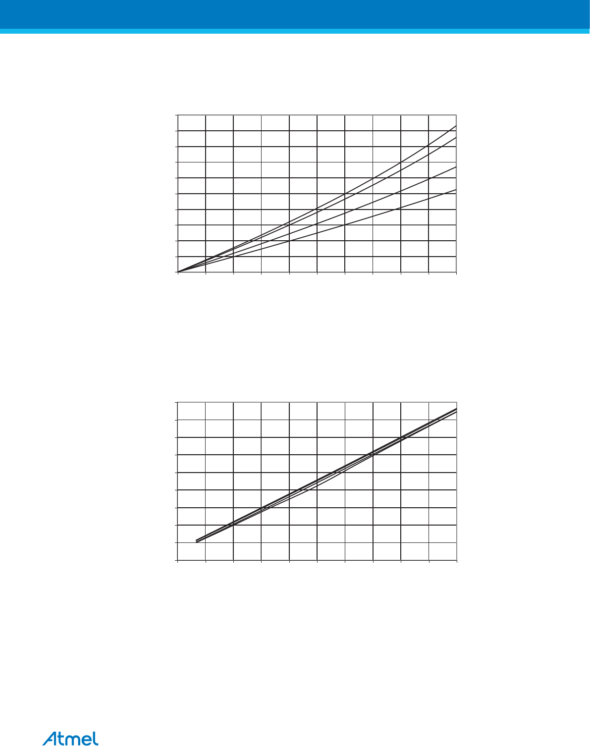
Figure 33-21 I/O Pin Output Voltage vs. Sink Current (VCC = 3V)
105 °C
85 °C
25 °C
-40 °C
I/O PIN OUTP UT VOLTAGE vs . SINK CURRENT
NORMAL P OWER P INS
0
0.1
0.2
0.3
0.4
0.5
0.6
0.7
0.8
0.9
1
0 2 4 6 8 10 12 14 16 18 20
IOL(mA)
VOL (V)
33.1.8. Pin Threshold and Hysteresis
Figure 33-22 I/O Pin Input Threshold vs. VCC (VIH , I/O Pin Read as ‘1’)
I/O PIN INPUT THRESHOLD VOLTAGE vs. VCC
VIH, IO P IN READ AS '1'
105 °C
85 °C
25 °C
-40 °C
1.2
1.4
1.6
1.8
2
2.2
2.4
2.6
2.8
3
2.5 2.8 3.1 3.4 3.7 4 4.3 4.6 4.9 5.2 5.5
VCC (V)
Thre s hold (V)
Atmel ATmega8A [DATASHEET]
Atmel-8159F-8-bit AVR Microcontroller_Datasheet_Complete-09/2015
362
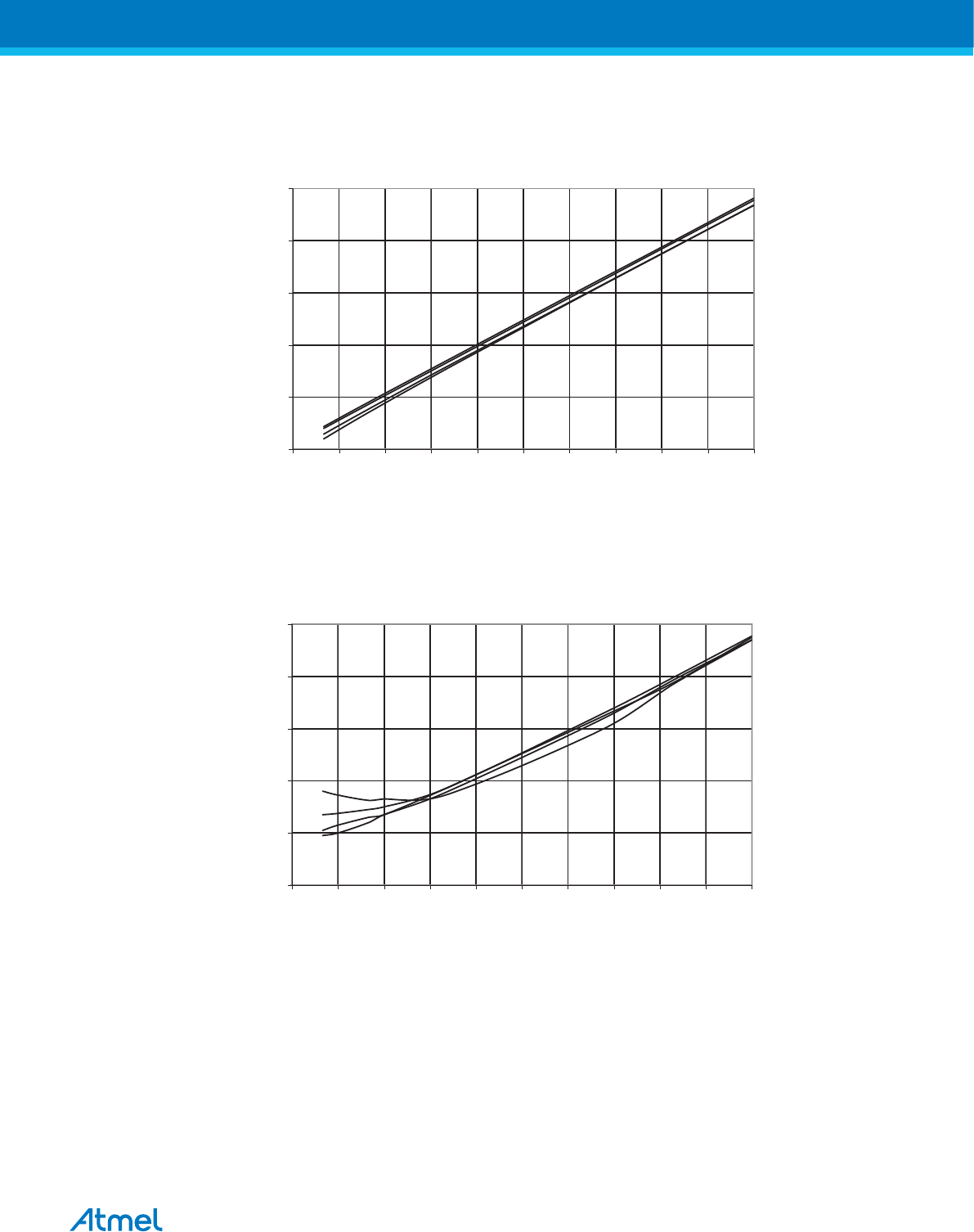
Figure 33-23 I/O Pin Input Threshold vs. VCC (VIL, I/O Pin Read as ‘0’)
I/O PIN INPUT THRESHOLD VOLTAGE vs. VCC
VIL, IO P IN READ AS '0'
105 °C
85 °C
25 °C
-40 °C
1
1.3
1.6
1.9
2.2
2.5
2.5 2.8 3.1 3.4 3.7 4 4.3 4.6 4.9 5.2 5.5
VCC (V)
Thre s hold (V)
Figure 33-24 I/O Pin Input Hysteresis vs. VCC
I/O PIN INPUT HYSTERESIS vs. VCC
105 °C
85 °C
25 °C
-40 °C
0.25
0.3
0.35
0.4
0.45
0.5
2.5 2.8 3.1 3.4 3.7 4 4.3 4.6 4.9 5.2 5.5
VCC (V)
Input Hyste re sis (mV)
Atmel ATmega8A [DATASHEET]
Atmel-8159F-8-bit AVR Microcontroller_Datasheet_Complete-09/2015
363
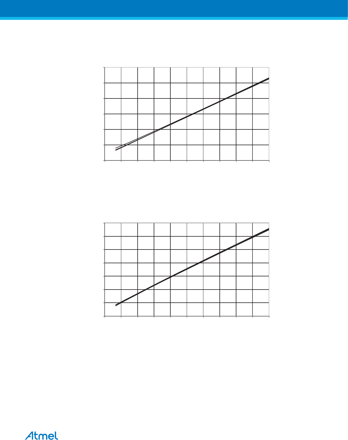
Figure 33-25 Reset Pin as I/O - Input Threshold vs. VCC (VIH , I/O Pin Read as ‘1’)
I/O PIN INPUT THRESHOLD VOLTAGE vs. VCC
VIH, IO P IN READ AS '1'
105 °C
85 °C
25 °C
-40 °C
1.3
1.6
1.9
2.2
2.5
2.8
3.1
2.5 2.8 3.1 3.4 3.7 4 4.3 4.6 4.9 5.2 5.5
VCC (V)
Thre s hold (V)
Figure 33-26 Reset Pin as I/O - Input Threshold vs. VCC (VIL, I/O Pin Read as ‘0’)
I/O PIN INPUT THRESHOLD VOLTAGE vs. VCC
VIL, IO P IN READ AS '0'
105 °C
85 °C
25 °C
-40 °C
0.9
1.1
1.3
1.5
1.7
1.9
2.1
2.3
2.5 2.8 3.1 3.4 3.7 4 4.3 4.6 4.9 5.2 5.5
VCC (V)
Thre s hold (V)
Atmel ATmega8A [DATASHEET]
Atmel-8159F-8-bit AVR Microcontroller_Datasheet_Complete-09/2015
364
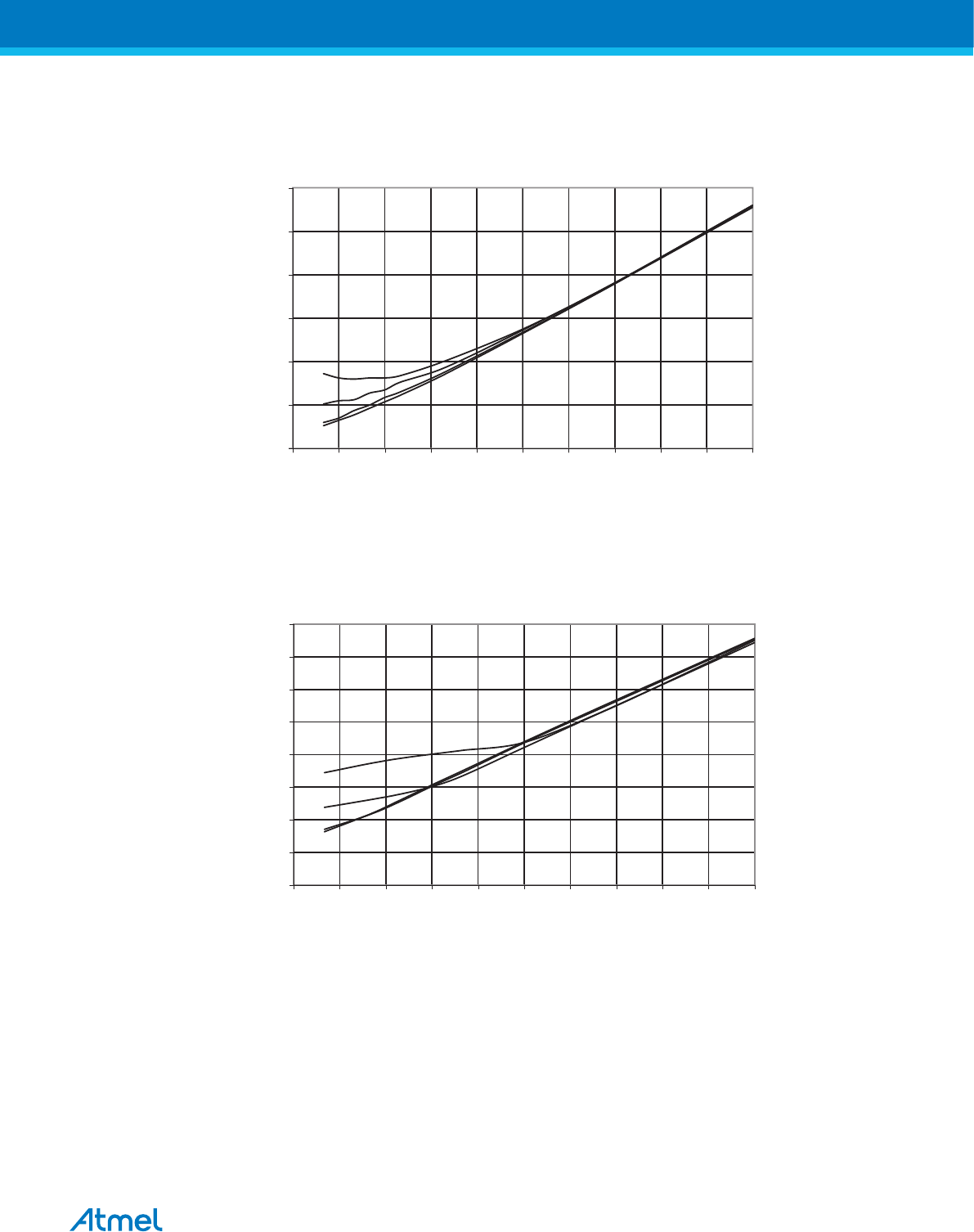
Figure 33-27 Reset Pin as I/O - Pin Hysteresis vs. VCC
RESET P IN AS IO, INPUT HYS TERESIS vs. VCC
VIL, IO P IN READ AS "0"
105 °C
85 °C
25 °C
-40 °C
0.4
0.45
0.5
0.55
0.6
0.65
0.7
2.5 2.8 3.1 3.4 3.7 4 4.3 4.6 4.9 5.2 5.5
VCC (V)
Input Hyste re sis (mV)
Figure 33-28 Reset Input Threshold vs. VCC (VIH , Reset Pin Read as ‘1’)
RESET INP UT THRESHOLD VOLTAGE vs . VCC
VIH, IO P IN READ AS '1'
105 °C
85 °C
25 °C
-40 °C
0.9
1.1
1.3
1.5
1.7
1.9
2.1
2.3
2.5
2.5 2.8 3.1 3.4 3.7 4 4.3 4.6 4.9 5.2 5.5
VCC (V)
Thre s hold (V)
Atmel ATmega8A [DATASHEET]
Atmel-8159F-8-bit AVR Microcontroller_Datasheet_Complete-09/2015
365
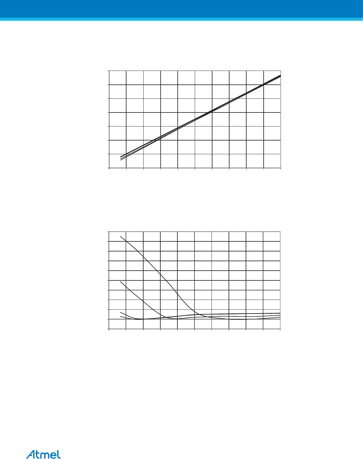
Figure 33-29 Reset Input Threshold vs. VCC (VIL, Reset Pin Read as ‘0’)
RESET INP UT THRESHOLD VOLTAGE vs . VCC
VIL, IO P IN READ AS '0'
105 °C
85 °C
25 °C
-40 °C
1
1.2
1.4
1.6
1.8
2
2.2
2.4
2.5 2.8 3.1 3.4 3.7 4 4.3 4.6 4.9 5.2 5.5
VCC (V)
Thres hold (V)
Figure 33-30 Reset Pin Input Hysteresis vs. VCC
RESET P IN INPUT HYS TERESIS vs. VCC
105 °C
85 °C
25 °C
-40 °C
0
0.05
0.1
0.15
0.2
0.25
0.3
0.35
0.4
0.45
0.5
2.5 2.8 3.1 3.4 3.7 4 4.3 4.6 4.9 5.2 5.5
VCC (V)
Input Hyste re sis (mV)
Atmel ATmega8A [DATASHEET]
Atmel-8159F-8-bit AVR Microcontroller_Datasheet_Complete-09/2015
366
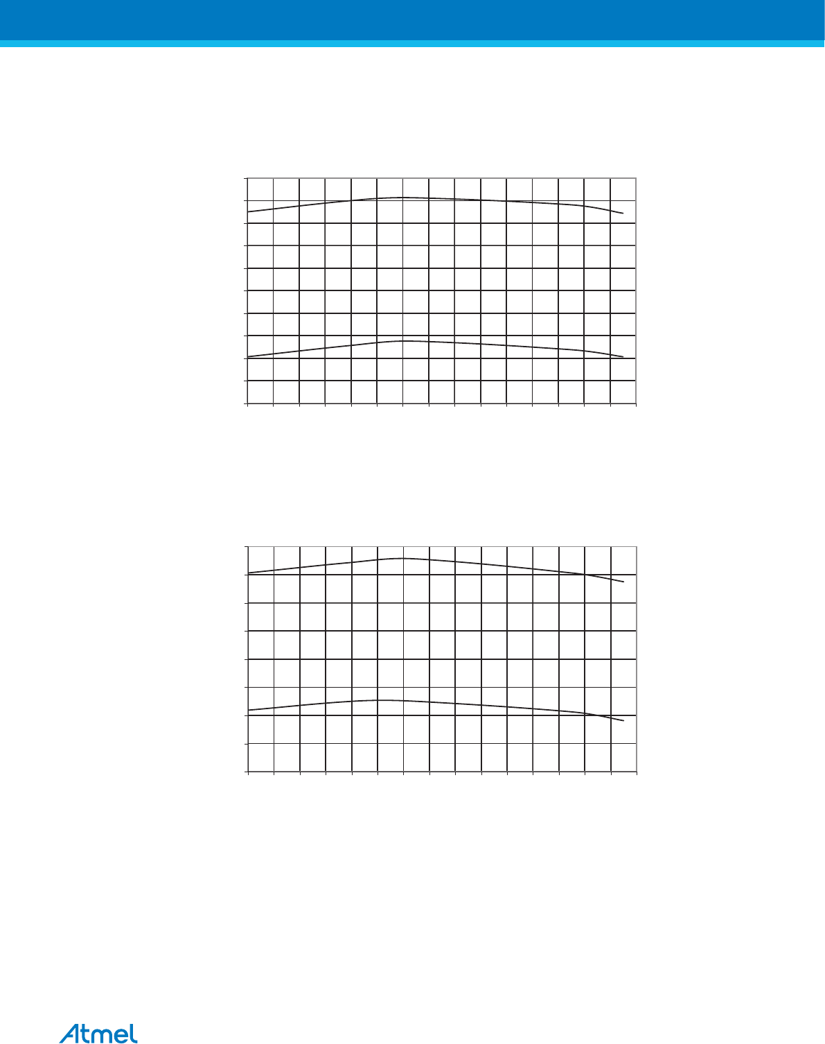
33.1.9. BOD Threshold
Figure 33-31 BOD Threshold vs. Temperature (VCC = 4.3V)
BOD THRESHOLDS vs. TEMP ERATURE
Rising Vcc
Fa lling Vcc
3.8
3.82
3.84
3.86
3.88
3.9
3.92
3.94
3.96
3.98
4
-40 -30 -20 -10 0 10 20 30 40 50 60 70 80 90 100 110
Tempe rature (°C)
Thre s hold (V)
Figure 33-32 BOD Threshold vs. Temperature (VCC = 2.7V)
BOD THRESHOLDS vs. TEMP ERATURE
Rising Vcc
Fa lling Vcc
2.47
2.49
2.51
2.53
2.55
2.57
2.59
2.61
2.63
-40 -30 -20 -10 0 10 20 30 40 50 60 70 80 90 100 110
Tempe rature (°C)
Thre s hold (V)
Atmel ATmega8A [DATASHEET]
Atmel-8159F-8-bit AVR Microcontroller_Datasheet_Complete-09/2015
367
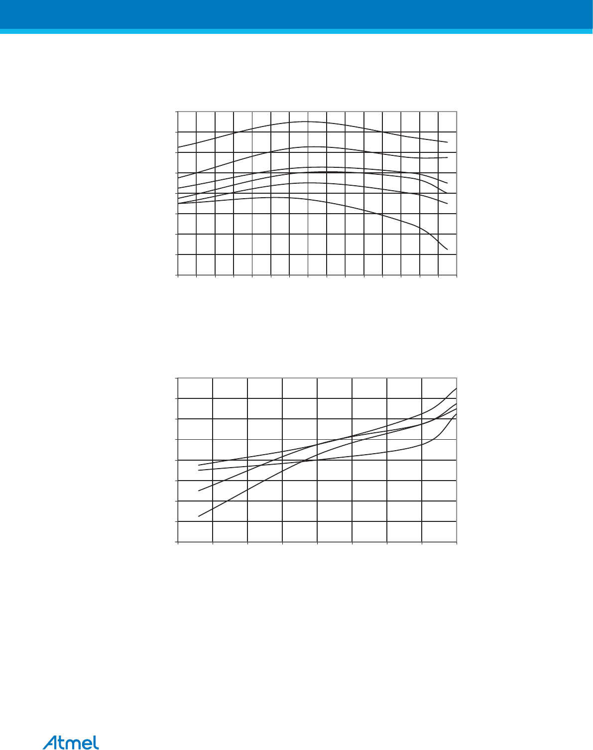
Figure 33-33 Bandgap Voltage vs. Temperature
BANDGAP VOLTAGE vs . TEMPERATURE
5.5V
5.0V
4.0V
3.3V
2.7V
1.8V
1.175
1.18
1.185
1.19
1.195
1.2
1.205
1.21
1.215
-40 -30 -20 -10 0 10 20 30 40 50 60 70 80 90 100 110
Tempe rature (°C)
Bandgap Voltage (V)
Figure 33-34 Bandgap Voltage vs. VCC
CALIB BANDGAP VOLTAGE vs . VCC
105 °C
85 °C
25 °C
-40 °C
1.175
1.18
1.185
1.19
1.195
1.2
1.205
1.21
1.215
1.5 2 2.5 3 3.5 4 4.5 5 5.5
VCC (V)
Bandga p Voltage (V)
Atmel ATmega8A [DATASHEET]
Atmel-8159F-8-bit AVR Microcontroller_Datasheet_Complete-09/2015
368
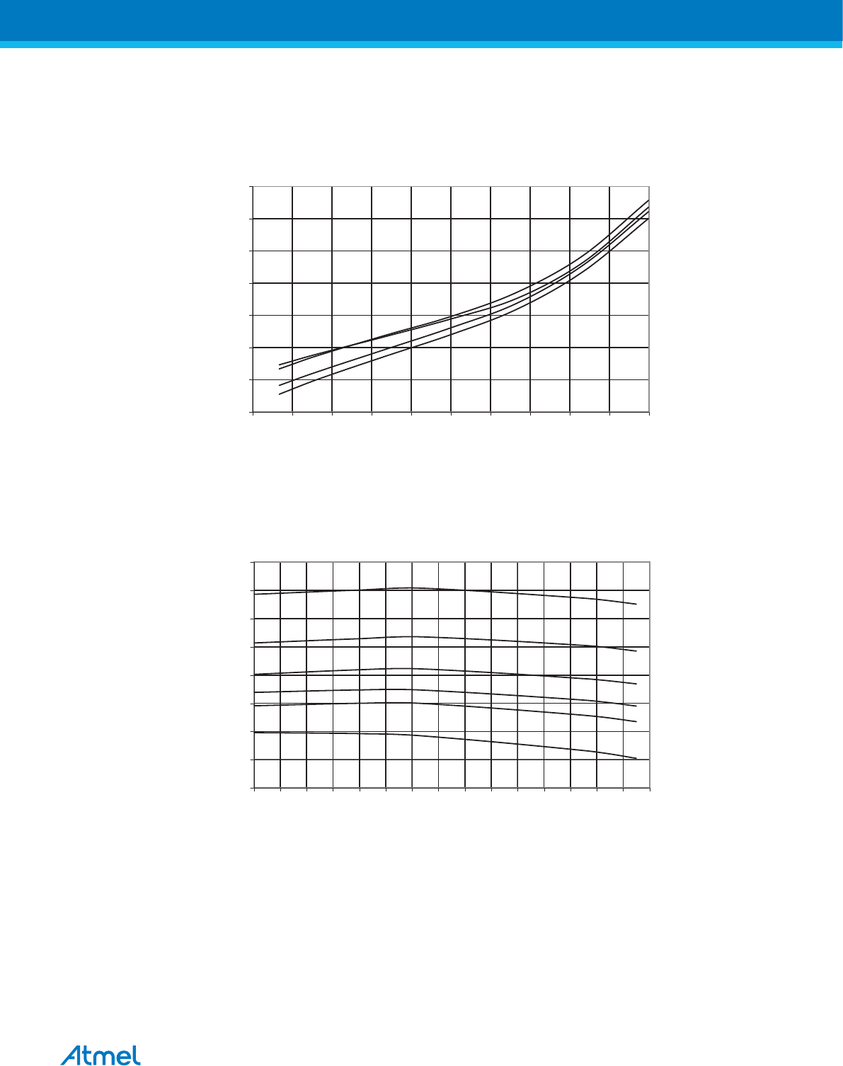
33.1.10. Internal Oscillator Speed
Figure 33-35 Watchdog Oscillator Frequency vs. VCC
WATCHDOG OSCILLATOR FREQUENCY vs . OP ERATING VOLTAGE
105 °C
85 °C
25 °C
-40 °C
980
1000
1020
1040
1060
1080
1100
1120
2.5 2.8 3.1 3.4 3.7 4 4.3 4.6 4.9 5.2 5.5
VCC (V)
FRC (kHz)
Figure 33-36 Watchdog Oscillator Frequency vs. Temperature
WATCHDOG OSCILLATOR FREQUENCY vs . TEMPERATURE
5.5 V
5.0 V
4.5 V
4.0 V
3.6 V
2.7 V
970
990
1010
1030
1050
1070
1090
1110
1130
-40 -30 -20 -10 0 10 20 30 40 50 60 70 80 90 100 110
Tempe rature (°C)
FRC (kHz)
Atmel ATmega8A [DATASHEET]
Atmel-8159F-8-bit AVR Microcontroller_Datasheet_Complete-09/2015
369
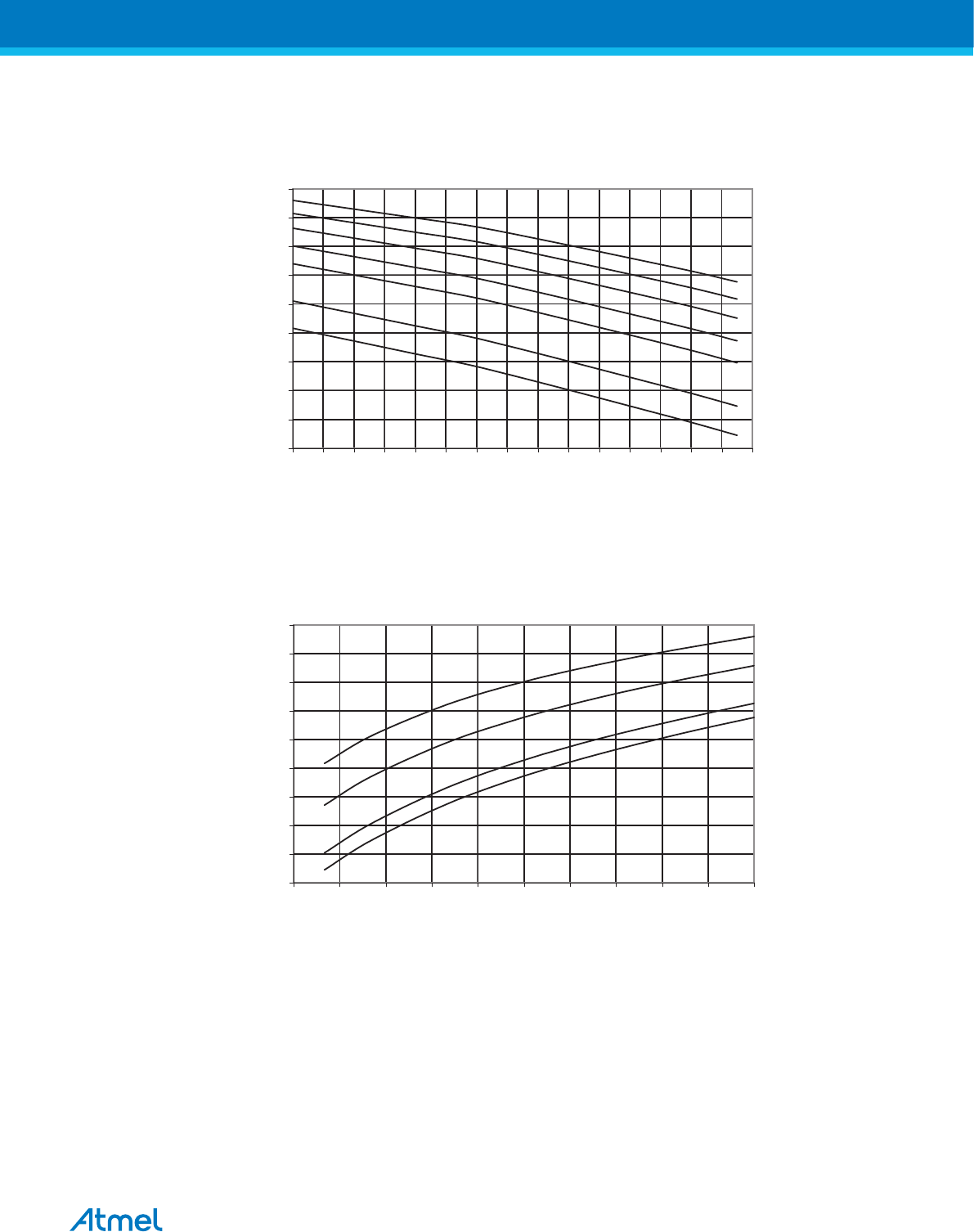
Figure 33-37 Calibrated 8MHz RC Oscillator vs. Temperature
CALIBRATED 8MHz RC OSCILLATOR FREQUENCY vs . TEMPERATURE
5.5 V
5.0 V
4.5 V
4.0 V
3.6 V
3.0 V
2.7 V
6.6
6.8
7
7.2
7.4
7.6
7.8
8
8.2
8.4
-40 -30 -20 -10 0 10 20 30 40 50 60 70 80 90 100 110
Tempe rature (°C)
FRC (MHz)
Figure 33-38 Calibrated 8MHz RC Oscillator vs. VCC
CALIBRATED 8MHz RC OSCILLATOR FREQUENCY vs . OP ERATING
VOLTAGE
105 °C
85 °C
25 °C
-40 °C
6.6
6.8
7
7.2
7.4
7.6
7.8
8
8.2
8.4
2.5 2.8 3.1 3.4 3.7 4 4.3 4.6 4.9 5.2 5.5
VCC (V)
FRC (MHz)
Atmel ATmega8A [DATASHEET]
Atmel-8159F-8-bit AVR Microcontroller_Datasheet_Complete-09/2015
370
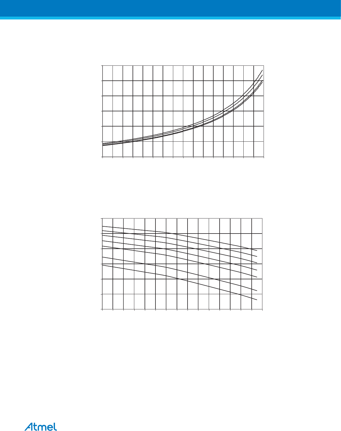
Figure 33-39 Calibrated 8MHz RC Oscillator vs. OSCCAL Value
CALIBRATED 8MHz RC OSCILLATOR FREQUENCY vs . OS CCAL VALUE
105 °C
85 °C
25 °C
-40 °C
2
4
6
8
10
12
14
0 16 32 48 64 80 96 112 128 144 160 176 192 208 224 240 256
OS CCAL (X1)
FRC (MHz)
Figure 33-40 Calibrated 4MHz RC Oscillator vs. Temperature
CALIBRATED 4MHz RC OSCILLATOR FREQUENCY vs . TEMPERATURE
5.5 V
5.0 V
4.5 V
4.0 V
3.6 V
3.0 V
2.7 V
3.55
3.65
3.75
3.85
3.95
4.05
4.15
-40 -30 -20 -10 0 10 20 30 40 50 60 70 80 90 100 110
Tempe rature (°C)
FRC (MHz)
Atmel ATmega8A [DATASHEET]
Atmel-8159F-8-bit AVR Microcontroller_Datasheet_Complete-09/2015
371
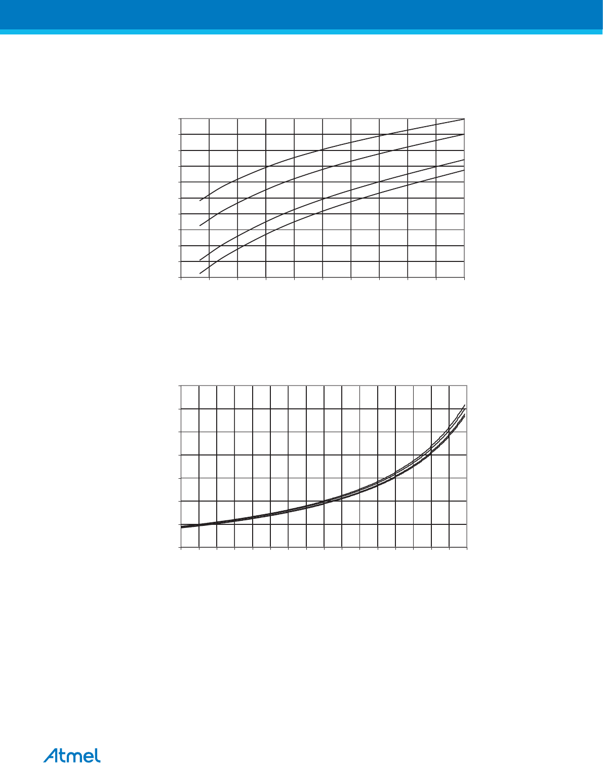
Figure 33-41 Calibrated 4MHz RC Oscillator vs. VCC
CALIBRATED 4MHz RC OSCILLATOR FREQUENCY vs . OP ERATING
VOLTAGE
105 °C
85 °C
25 °C
-40 °C
3.6
3.65
3.7
3.75
3.8
3.85
3.9
3.95
4
4.05
4.1
2.5 2.8 3.1 3.4 3.7 4 4.3 4.6 4.9 5.2 5.5
VCC (V)
FRC (MHz)
Figure 33-42 Calibrated 4MHz RC Oscillator vs. OSCCAL Value
CALIBRATED 4MHz RC OSCILLATOR FREQUENCY vs . OS CCAL VALUE
105 °C
85 °C
25 °C
-40 °C
1
2
3
4
5
6
7
8
0 16 32 48 64 80 96 112 128 144 160 176 192 208 224 240 256
OS CCAL (X1)
FRC (MHz)
Atmel ATmega8A [DATASHEET]
Atmel-8159F-8-bit AVR Microcontroller_Datasheet_Complete-09/2015
372
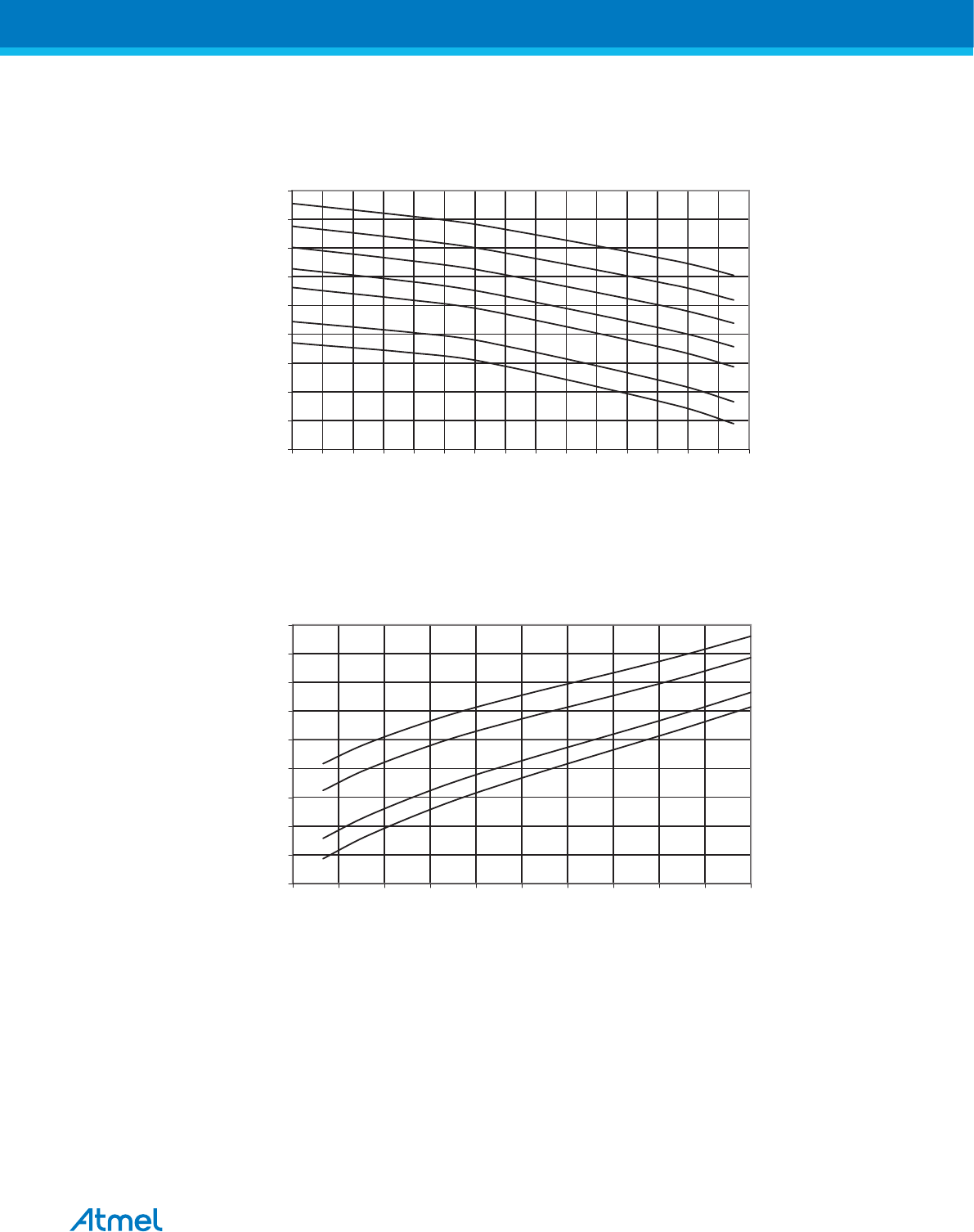
Figure 33-43 Calibrated 2MHz RC Oscillator vs. Temperature
CALIBRATED 2MHz RC OSCILLATOR FREQUENCY vs . TEMPERATURE
5.5 V
5.0 V
4.5 V
4.0 V
3.6 V
3.0 V
2.7 V
1.78
1.81
1.84
1.87
1.9
1.93
1.96
1.99
2.02
2.05
-40 -30 -20 -10 0 10 20 30 40 50 60 70 80 90 100 110
Tempe ra ture (°C)
FRC (MHz)
Figure 33-44 Calibrated 2MHz RC Oscillator vs. VCC
CALIBRATED 2MHz RC OSCILLATOR FREQUENCY vs . OPERATING
VOLTAGE
105 °C
85 °C
25 °C
-40 °C
1.8
1.83
1.86
1.89
1.92
1.95
1.98
2.01
2.04
2.07
2.5 2.8 3.1 3.4 3.7 4 4.3 4.6 4.9 5.2 5.5
VCC (V)
FRC (MHz)
Atmel ATmega8A [DATASHEET]
Atmel-8159F-8-bit AVR Microcontroller_Datasheet_Complete-09/2015
373
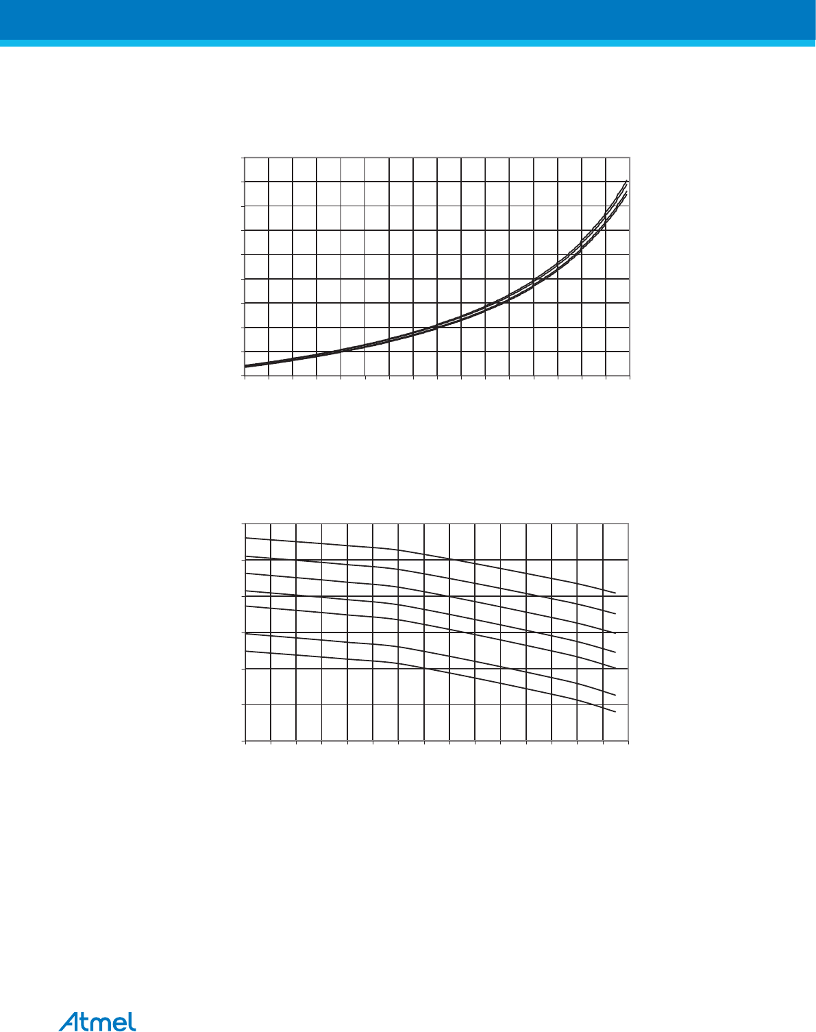
Figure 33-45 Calibrated 2MHz RC Oscillator vs. OSCCAL Value
CALIBRATED 2MHz RC OSCILLATOR FREQUENCY vs . OS CCAL
VALUE
105 °C
85 °C
25 °C
-40 °C
0.8
1.1
1.4
1.7
2
2.3
2.6
2.9
3.2
3.5
0 16 32 48 64 80 96 112 128 144 160 176 192 208 224 240 256
OS CCAL (X1)
FRC (MHz)
Figure 33-46 Calibrated 1MHz RC Oscillator vs. Temperature
CALIBRATED 1MHz RC OSCILLATOR FREQUENCY vs . TEMPERATURE
5.5 V
5.0 V
4.5 V
4.0 V
3.6 V
3.0 V
2.7 V
0.91
0.93
0.95
0.97
0.99
1.01
1.03
-40 -30 -20 -10 0 10 20 30 40 50 60 70 80 90 100 110
Tempe rature (°C)
FRC (MHz)
Atmel ATmega8A [DATASHEET]
Atmel-8159F-8-bit AVR Microcontroller_Datasheet_Complete-09/2015
374
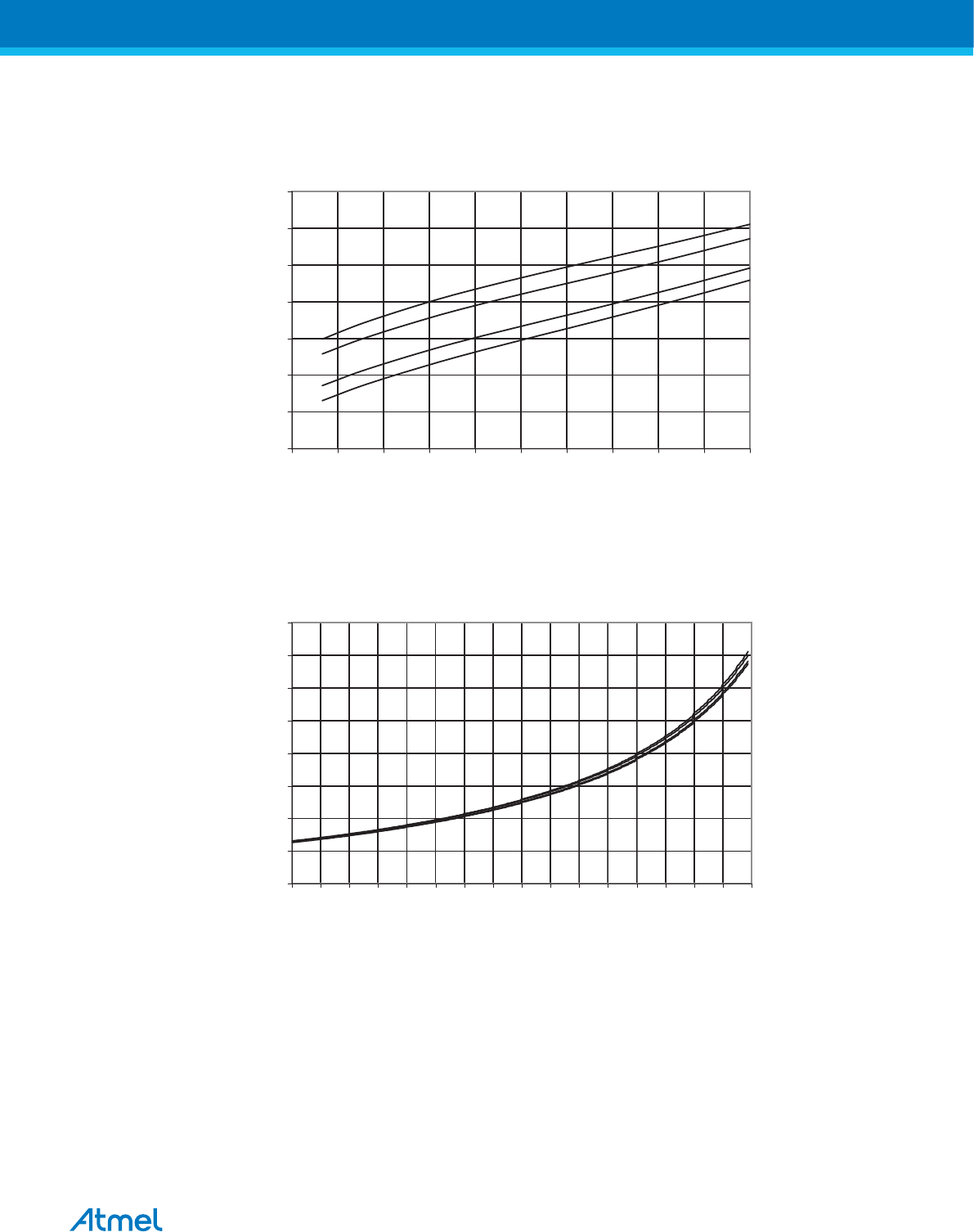
Figure 33-47 Calibrated 1MHz RC Oscillator vs. VCC
CALIBRATED 1 MHz RC OSCILLATOR FREQUENCY vs. OP ERATING
VOLTAGE
105 °C
85 °C
25 °C
-40 °C
0.9
0.92
0.94
0.96
0.98
1
1.02
1.04
2.5 2.8 3.1 3.4 3.7 4 4.3 4.6 4.9 5.2 5.5
VCC (V)
FRC (MHz)
Figure 33-48 Calibrated 1MHz RC Oscillator vs. OSCCAL Value
CALIBRATED 1MHz RC OSCILLATOR FREQUENCY vs . OS CCAL VALUE
105 °C
85 °C
25 °C
-40 °C
0.2
0.4
0.6
0.8
1
1.2
1.4
1.6
1.8
0 16 32 48 64 80 96 112 128 144 160 176 192 208 224 240 256
OS CCAL (X1)
FRC (MHz)
Atmel ATmega8A [DATASHEET]
Atmel-8159F-8-bit AVR Microcontroller_Datasheet_Complete-09/2015
375
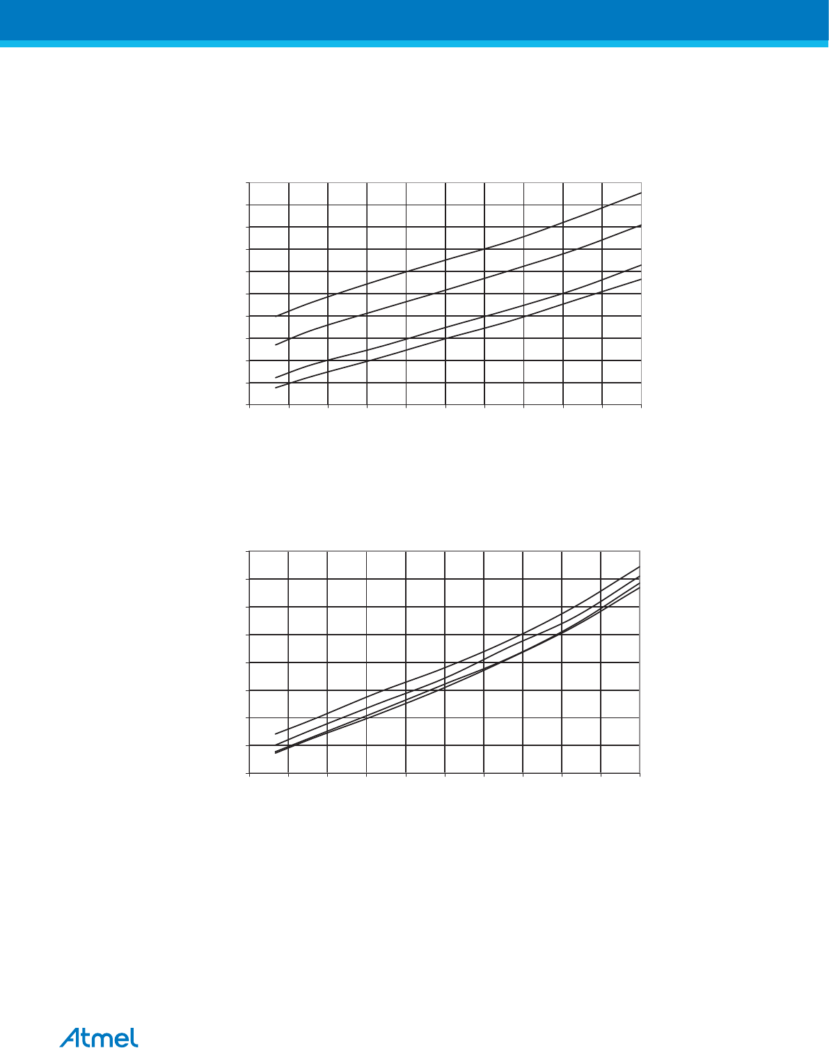
33.1.11. Current Consumption of Peripheral Units
Figure 33-49 Brown-out Detector Current vs. VCC
BROWNOUT DETECTOR CURRENT vs . VCC
105 °C
85 °C
25 °C
-40 °C
8
9
10
11
12
13
14
15
16
17
18
2.5 2.8 3.1 3.4 3.7 4 4.3 4.6 4.9 5.2 5.5
VCC (V)
ICC (uA)
Figure 33-50 ADC Current vs. VCC (AREF = AVCC)
ACTIVE S UP P LY CURRENT WITH ADC AT 50KHz vs. VCC
105 °C
85 °C
25 °C
-40 °C
140
160
180
200
220
240
260
280
300
2.5 2.8 3.1 3.4 3.7 4 4.3 4.6 4.9 5.2 5.5
VCC (V)
ICC (uA)
Atmel ATmega8A [DATASHEET]
Atmel-8159F-8-bit AVR Microcontroller_Datasheet_Complete-09/2015
376
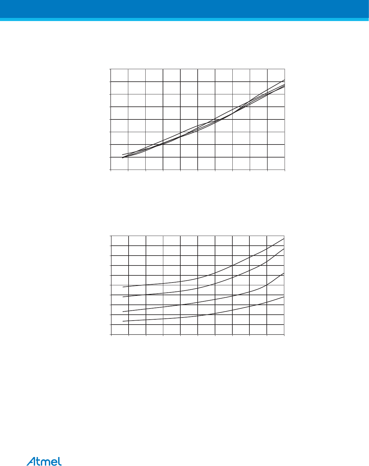
Figure 33-51 Watchdog Timer Current vs. VCC
WATCHDOG TIMER CURRENT vs . VCC
4
6
8
10
12
14
16
18
20
2.5 2.8 3.1 3.4 3.7 4 4.3 4.6 4.9 5.2 5.5
VCC (V)
ICC (uA)
105 °C
85 °C
25 °C
-40 °C
Figure 33-52 Analog Comparator Current vs. VCC
ANALOG COMPARATOR CURRENT vs . VCC
32
36
40
44
48
52
56
60
64
68
72
2.5 2.8 3.1 3.4 3.7 4 4.3 4.6 4.9 5.2 5.5
VCC (V)
ICC (mA)
105 °C
85 °C
25 °C
-40 °C
Atmel ATmega8A [DATASHEET]
Atmel-8159F-8-bit AVR Microcontroller_Datasheet_Complete-09/2015
377
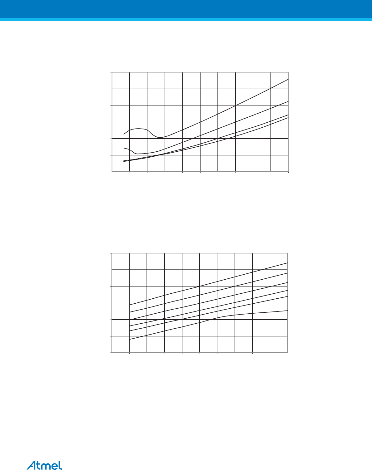
Figure 33-53 Programming Current vs. VCC
EEPROM WRITE CURRENT vs . Vcc
Ext Clk
105 °C
85 °C
25 °C
-40 °C
0
1
2
3
4
5
6
2.5 2.8 3.1 3.4 3.7 4 4.3 4.6 4.9 5.2 5.5
VCC (V)
ICC (mA)
33.1.12. Current Consumption in Reset and Reset Pulsewidth
Figure 33-54 Reset Supply Current vs. VCC (0.1 - 1.0MHz, Excluding Current Through the Reset Pull-up)
RESET S UPPLY CURRENT vs . VCC
EXCLUDING CURRENT THROUGH THE RES ET P ULLUP
5.5 V
5.0 V
4.5 V
4.0 V
3.6 V
2.7 V
0
0.5
1
1.5
2
2.5
3
0 0.1 0.2 0.3 0.4 0.5 0.6 0.7 0.8 0.9 1
Fre quency (MHz)
ICC (mA)
Atmel ATmega8A [DATASHEET]
Atmel-8159F-8-bit AVR Microcontroller_Datasheet_Complete-09/2015
378
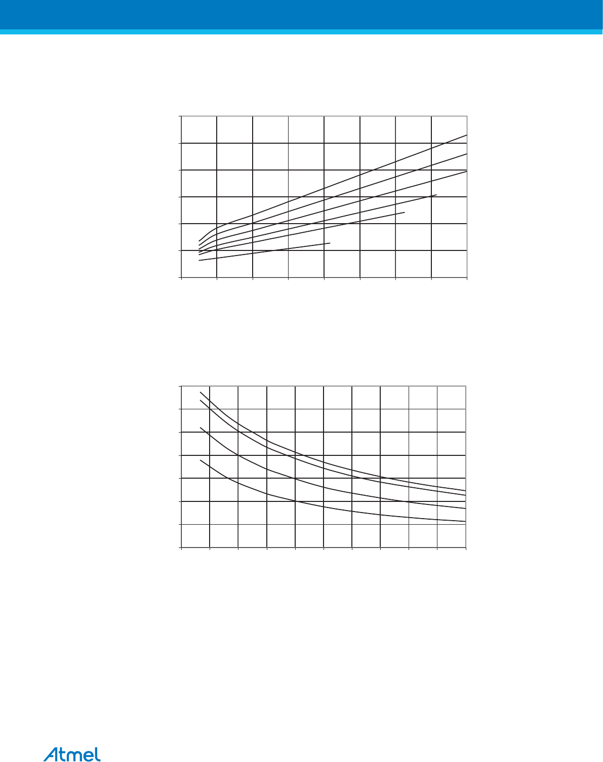
Figure 33-55 Reset Supply Current vs. VCC (1 - 16MHz, Excluding Current Through the Reset Pull-up)
5.5 V
5.0 V
4.5 V
4.0 V
3.6 V
2.7 V
RESET S UP PLY CURRENT vs . VCC
EXCLUDING CURRENT THROUGH THE RES ET P ULLUP
0
2
4
6
8
10
12
0 2 4 6 8 10 12 14 16
Fre quency (MHz)
ICC (mA)
Figure 33-56 Minimum Reset Pulsewidth vs. VCC
MINIMUM RESET P ULSE WIDTH vs. VCC
105 °C
85 °C
25 °C
-40 °C
100
200
300
400
500
600
700
800
2.5 2.8 3.1 3.4 3.7 4 4.3 4.6 4.9 5.2 5.5
VCC (V)
Puls e width (ns )
Atmel ATmega8A [DATASHEET]
Atmel-8159F-8-bit AVR Microcontroller_Datasheet_Complete-09/2015
379
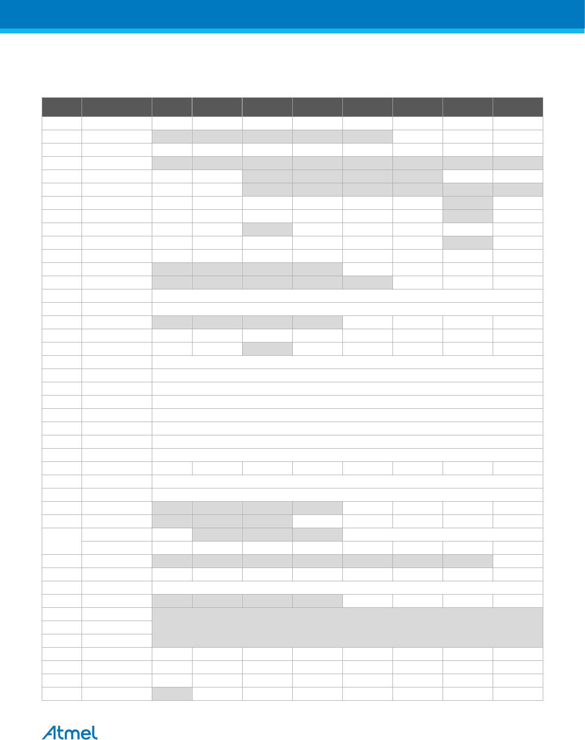
34. Register Summary
Address Name Bit 7 Bit 6 Bit 5 Bit 4 Bit 3 Bit 2 Bit 1 Bit 0
0x3F (0x5F) SREG I T H S V N Z C
0x3E (0x5E) SPH – – – – – SP10 SP9 SP8
0x3D (0x5D) SPL SP7 SP6 SP5 SP4 SP3 SP2 SP1 SP0
0x3C (0x5C) Reserved – – – – – – – –
0x3B (0x5B) GICR INT1 INT0 – – – – IVSEL IVCE
0x3A (0x5A) GIFR INTF1 INTF0 – – – – – –
0x39 (0x59) TIMSK OCIE2 TOIE2 TICIE1 OCIE1A OCIE1B TOIE1 – TOIE0
0x38 (0x58) TIFR OCF2 TOV2 ICF1 OCF1A OCF1B TOV1 – TOV0
0x37 (0x57) SPMCR SPMIE RWWSB – RWWSRE BLBSET PGWRT PGERS SPMEN
0x36 (0x56) TWCR TWINT TWEA TWSTA TWSTO TWWC TWEN – TWIE
0x35 (0x55) MCUCR SE SM2 SM1 SM0 ISC11 ISC10 ISC01 ISC00
0x34 (0x54) MCUCSR – – – – WDRF BORF EXTRF PORF
0x33 (0x53) TCCR0 – – – – – CS02 CS01 CS00
0x32 (0x52) TCNT0 Timer/Counter0 (8 Bits)
0x31 (0x51) OSCCAL Oscillator Calibration Register
0x30 (0x50) SFIOR – – – – ACME PUD PSR2 PSR10
0x2F (0x4F) TCCR1A COM1A1 COM1A0 COM1B1 COM1B0 FOC1A FOC1B WGM11 WGM10
0x2E (0x4E) TCCR1B ICNC1 ICES1 – WGM13 WGM12 CS12 CS11 CS10
0x2D (0x4D) TCNT1H Timer/Counter1 – Counter Register High byte
0x2C (0x4C) TCNT1L Timer/Counter1 – Counter Register Low byte
0x2B (0x4B) OCR1AH Timer/Counter1 – Output Compare Register A High byte
0x2A (0x4A) OCR1AL Timer/Counter1 – Output Compare Register A Low byte
0x29 (0x49) OCR1BH Timer/Counter1 – Output Compare Register B High byte
0x28 (0x48) OCR1BL Timer/Counter1 – Output Compare Register B Low byte
0x27 (0x47) ICR1H Timer/Counter1 – Input Capture Register High byte
0x26 (0x46) ICR1L Timer/Counter1 – Input Capture Register Low byte
0x25 (0x45) TCCR2 FOC2 WGM20 COM21 COM20 WGM21 CS22 CS21 CS20
0x24 (0x44) TCNT2 Timer/Counter2 (8 Bits)
0x23 (0x43) OCR2 Timer/Counter2 Output Compare Register
0x22 (0x42) ASSR – – – – AS2 TCN2UB OCR2UB TCR2UB
0x21 (0x41) WDTCR – – – WDCE WDE WDP2 WDP1 WDP0
0x20(1)
(0x40)(1)
UBRRH URSEL – – – UBRR[11:8]
UCSRC URSEL UMSEL UPM1 UPM0 USBS UCSZ1 UCSZ0 UCPOL
0x1F (0x3F) EEARH – – – – – – – EEAR8
0x1E (0x3E) EEARL EEAR7 EEAR6 EEAR5 EEAR4 EEAR3 EEAR2 EEAR1 EEAR0
0x1D (0x3D) EEDR EEPROM Data Register
0x1C (0x3C) EECR – – – – EERIE EEMWE EEWE EERE
0x1B (0x3B) Reserved
0x1A (0x3A) Reserved
0x19 (0x39) Reserved
0x18 (0x38) PORTB PORTB7 PORTB6 PORTB5 PORTB4 PORTB3 PORTB2 PORTB1 PORTB0
0x17 (0x37) DDRB DDB7 DDB6 DDB5 DDB4 DDB3 DDB2 DDB1 DDB0
0x16 (0x36) PINB PINB7 PINB6 PINB5 PINB4 PINB3 PINB2 PINB1 PINB0
0x15 (0x35) PORTC – PORTC6 PORTC5 PORTC4 PORTC3 PORTC2 PORTC1 PORTC0
Atmel ATmega8A [DATASHEET]
Atmel-8159F-8-bit AVR Microcontroller_Datasheet_Complete-09/2015
380
Address Name Bit 7 Bit 6 Bit 5 Bit 4 Bit 3 Bit 2 Bit 1 Bit 0
0x14 (0x34) DDRC – DDC6 DDC5 DDC4 DDC3 DDC2 DDC1 DDC0
0x13 (0x33) PINC – PINC6 PINC5 PINC4 PINC3 PINC2 PINC1 PINC0
0x12 (0x32) PORTD PORTD7 PORTD6 PORTD5 PORTD4 PORTD3 PORTD2 PORTD1 PORTD0
0x11 (0x31) DDRD DDD7 DDD6 DDD5 DDD4 DDD3 DDD2 DDD1 DDD0
0x10 (0x30) PIND PIND7 PIND6 PIND5 PIND4 PIND3 PIND2 PIND1 PIND0
0x0F (0x2F) SPDR SPI Data Register
0x0E (0x2E) SPSR SPIF WCOL – – – – – SPI2X
0x0D (0x2D) SPCR SPIE SPE DORD MSTR CPOL CPHA SPR1 SPR0
0x0C (0x2C) UDR USART I/O Data Register
0x0B (0x2B) UCSRA RXC TXC UDRE FE DOR PE U2X MPCM
0x0A (0x2A) UCSRB RXCIE TXCIE UDRIE RXEN TXEN UCSZ2 RXB8 TXB8
0x09 (0x29) UBRRL USART Baud Rate Register Low byte
0x08 (0x28) ACSR ACD ACBG ACO ACI ACIE ACIC ACIS1 ACIS0
0x07 (0x27) ADMUX REFS1 REFS0 ADLAR – MUX3 MUX2 MUX1 MUX0
0x06 (0x26) ADCSRA ADEN ADSC ADFR ADIF ADIE ADPS2 ADPS1 ADPS0
0x05 (0x25) ADCH ADC Data Register High byte
0x04 (0x24) ADCL ADC Data Register Low byte
0x03 (0x23) TWDR Two-wire Serial Interface Data Register
0x02 (0x22) TWAR TWA6 TWA5 TWA4 TWA3 TWA2 TWA1 TWA0 TWGCE
0x01 (0x21) TWSR TWS7 TWS6 TWS5 TWS4 TWS3 – TWPS1 TWPS0
0x00 (0x20) TWBR Two-wire Serial Interface Bit Rate Register
Note:
1. Refer to the USART description for details on how to access UBRRH and UCSRC.
2. For compatibility with future devices, reserved bits should be written to zero if accessed. Reserved
I/O memory addresses should never be written.
3. Some of the Status Flags are cleared by writing a logical one to them. Note that the CBI and SBI
instructions will operate on all bits in the I/O Register, writing a one back into any flag read as set,
thus clearing the flag. The CBI and SBI instructions work with registers 0x00 to 0x1F only.
Atmel ATmega8A [DATASHEET]
Atmel-8159F-8-bit AVR Microcontroller_Datasheet_Complete-09/2015
381

35. Instruction Set Summary
ARITHMETIC AND LOGIC INSTRUCTIONS
Mnemonics Operands Description Operation Flags #Clocks
ADD Rd, Rr Add two Registers Rd ← Rd + Rr Z,C,N,V,H 1
ADC Rd, Rr Add with Carry two Registers Rd ← Rd + Rr + C Z,C,N,V,H 1
ADIW Rdl,K Add Immediate to Word Rdh:Rdl ← Rdh:Rdl + K Z,C,N,V,S 2
SUB Rd, Rr Subtract two Registers Rd ← Rd - Rr Z,C,N,V,H 1
SUBI Rd, K Subtract Constant from Register Rd ← Rd - K Z,C,N,V,H 1
SBC Rd, Rr Subtract with Carry two Registers Rd ← Rd - Rr - C Z,C,N,V,H 1
SBCI Rd, K Subtract with Carry Constant from Reg. Rd ← Rd - K - C Z,C,N,V,H 1
SBIW Rdl,K Subtract Immediate from Word Rdh:Rdl ← Rdh:Rdl - K Z,C,N,V,S 2
AND Rd, Rr Logical AND Registers Rd ← Rd · Rr Z,N,V 1
ANDI Rd, K Logical AND Register and Constant Rd ← Rd · K Z,N,V 1
OR Rd, Rr Logical OR Registers Rd ← Rd v Rr Z,N,V 1
ORI Rd, K Logical OR Register and Constant Rd ← Rd v K Z,N,V 1
EOR Rd, Rr Exclusive OR Registers Rd ← Rd ⊕ Rr Z,N,V 1
COM Rd One’s Complement Rd ← 0xFF - Rd Z,C,N,V 1
NEG Rd Two’s Complement Rd ← 0x00 - Rd Z,C,N,V,H 1
SBR Rd,K Set Bit(s) in Register Rd ← Rd v K Z,N,V 1
CBR Rd,K Clear Bit(s) in Register Rd ← Rd · (0xFF - K) Z,N,V 1
INC Rd Increment Rd ← Rd + 1 Z,N,V 1
DEC Rd Decrement Rd ← Rd - 1 Z,N,V 1
TST Rd Test for Zero or Minus Rd ← Rd · Rd Z,N,V 1
CLR Rd Clear Register Rd ← Rd ⊕ Rd Z,N,V 1
SER Rd Set Register Rd ← 0xFF None 1
MUL Rd, Rr Multiply Unsigned R1:R0 ← Rd x Rr Z,C 2
MULS Rd, Rr Multiply Signed R1:R0 ← Rd x Rr Z,C 2
MULSU Rd, Rr Multiply Signed with Unsigned R1:R0 ← Rd x Rr Z,C 2
FMUL Rd, Rr Fractional Multiply Unsigned R1:R0 ← (Rd x Rr) << 1 Z,C 2
FMULS Rd, Rr Fractional Multiply Signed R1:R0 ← (Rd x Rr) << 1 Z,C 2
FMULSU Rd, Rr Fractional Multiply Signed with Unsigned R1:R0 ← (Rd x Rr) << 1 Z,C 2
BRANCH INSTRUCTIONS
Mnemonics Operands Description Operation Flags #Clocks
RJMP k Relative Jump PC ← PC + k + 1 None 2
IJMP Indirect Jump to (Z) PC ← Z None 2
JMP(1) k Direct Jump PC ← k None 3
RCALL k Relative Subroutine Call PC ← PC + k + 1 None 3
Atmel ATmega8A [DATASHEET]
Atmel-8159F-8-bit AVR Microcontroller_Datasheet_Complete-09/2015
382

BRANCH INSTRUCTIONS
Mnemonics Operands Description Operation Flags #Clocks
ICALL Indirect Call to (Z) PC ← Z None 3
CALL(1) k Direct Subroutine Call PC ← k None 4
RET Subroutine Return PC ← STACK None 4
RETI Interrupt Return PC ← STACK I 4
CPSE Rd,Rr Compare, Skip if Equal if (Rd = Rr) PC ← PC + 2 or 3 None 1 / 2 / 3
CP Rd,Rr Compare Rd - Rr Z, N,V,C,H 1
CPC Rd,Rr Compare with Carry Rd - Rr - C Z, N,V,C,H 1
CPI Rd,K Compare Register with Immediate Rd - K Z, N,V,C,H 1
SBRC Rr, b Skip if Bit in Register Cleared if (Rr(b)=0) PC ← PC + 2 or 3 None 1 / 2 / 3
SBRS Rr, b Skip if Bit in Register is Set if (Rr(b)=1) PC ← PC + 2 or 3 None 1 / 2 / 3
SBIC P, b Skip if Bit in I/O Register Cleared if (P(b)=0) PC ← PC + 2 or 3 None 1 / 2 / 3
SBIS P, b Skip if Bit in I/O Register is Set if (P(b)=1) PC ← PC + 2 or 3 None 1 / 2 / 3
BRBS s, k Branch if Status Flag Set if (SREG(s) = 1) then PC←PC+k + 1 None 1 / 2
BRBC s, k Branch if Status Flag Cleared if (SREG(s) = 0) then PC←PC+k + 1 None 1 / 2
BREQ k Branch if Equal if (Z = 1) then PC ← PC + k + 1 None 1 / 2
BRNE k Branch if Not Equal if (Z = 0) then PC ← PC + k + 1 None 1 / 2
BRCS k Branch if Carry Set if (C = 1) then PC ← PC + k + 1 None 1 / 2
BRCC k Branch if Carry Cleared if (C = 0) then PC ← PC + k + 1 None 1 / 2
BRSH k Branch if Same or Higher if (C = 0) then PC ← PC + k + 1 None 1 / 2
BRLO k Branch if Lower if (C = 1) then PC ← PC + k + 1 None 1 / 2
BRMI k Branch if Minus if (N = 1) then PC ← PC + k + 1 None 1 / 2
BRPL k Branch if Plus if (N = 0) then PC ← PC + k + 1 None 1 / 2
BRGE k Branch if Greater or Equal, Signed if (N Å V= 0) then PC ← PC + k + 1 None 1 / 2
BRLT k Branch if Less Than Zero, Signed if (N Å V= 1) then PC ← PC + k + 1 None 1 / 2
BRHS k Branch if Half Carry Flag Set if (H = 1) then PC ← PC + k + 1 None 1 / 2
BRHC k Branch if Half Carry Flag Cleared if (H = 0) then PC ← PC + k + 1 None 1 / 2
BRTS k Branch if T Flag Set if (T = 1) then PC ← PC + k + 1 None 1 / 2
BRTC k Branch if T Flag Cleared if (T = 0) then PC ← PC + k + 1 None 1 / 2
BRVS k Branch if Overflow Flag is Set if (V = 1) then PC ← PC + k + 1 None 1 / 2
BRVC k Branch if Overflow Flag is Cleared if (V = 0) then PC ← PC + k + 1 None 1 / 2
BRIE k Branch if Interrupt Enabled if ( I = 1) then PC ← PC + k + 1 None 1 / 2
BRID k Branch if Interrupt Disabled if ( I = 0) then PC ← PC + k + 1 None 1 / 2
BIT AND BIT-TEST INSTRUCTIONS
Mnemonics Operands Description Operation Flags #Clocks
SBI P,b Set Bit in I/O Register I/O(P,b) ← 1 None 2
CBI P,b Clear Bit in I/O Register I/O(P,b) ← 0 None 2
Atmel ATmega8A [DATASHEET]
Atmel-8159F-8-bit AVR Microcontroller_Datasheet_Complete-09/2015
383

BIT AND BIT-TEST INSTRUCTIONS
Mnemonics Operands Description Operation Flags #Clocks
LSL Rd Logical Shift Left Rd(n+1) ← Rd(n), Rd(0) ← 0 Z,C,N,V 1
LSR Rd Logical Shift Right Rd(n) ← Rd(n+1), Rd(7) ← 0 Z,C,N,V 1
ROL Rd Rotate Left Through Carry Rd(0)←C,Rd(n+1)← Rd(n),C¬Rd(7) Z,C,N,V 1
ROR Rd Rotate Right Through Carry Rd(7)←C,Rd(n)← Rd(n+1),C←Rd(0) Z,C,N,V 1
ASR Rd Arithmetic Shift Right Rd(n) ← Rd(n+1), n=0:6 Z,C,N,V 1
SWAP Rd Swap Nibbles Rd(3:0)←Rd(7:4),Rd(7:4)¬Rd(3:0) None 1
BSET s Flag Set SREG(s) ← 1 SREG(s) 1
BCLR s Flag Clear SREG(s) ← 0 SREG(s) 1
BST Rr, b Bit Store from Register to T T ← Rr(b) T 1
BLD Rd, b Bit load from T to Register Rd(b) ← T None 1
SEC Set Carry C ← 1 C 1
CLC Clear Carry C ← 0 C 1
SEN Set Negative Flag N ← 1 N 1
CLN Clear Negative Flag N ← 0 N 1
SEZ Set Zero Flag Z ← 1 Z 1
CLZ Clear Zero Flag Z ← 0 Z 1
SEI Global Interrupt Enable I ← 1 I 1
CLI Global Interrupt Disable I ← 0 I 1
SES Set Signed Test Flag S ← 1 S 1
CLS Clear Signed Test Flag S ← 0 S 1
SEV Set Twos Complement Overflow. V ← 1 V 1
CLV Clear Twos Complement Overflow V ← 0 V 1
SET Set T in SREG T ← 1 T 1
CLT Clear T in SREG T ← 0 T 1
SEH Set Half Carry Flag in SREG H ← 1 H 1
CLH Clear Half Carry Flag in SREG H ← 0 H 1
DATA TRANSFER INSTRUCTIONS
Mnemonics Operands Description Operation Flags #Clocks
MOV Rd, Rr Move Between Registers Rd ← Rr None 1
MOVW Rd, Rr Copy Register Word Rd+1:Rd ← Rr+1:Rr None 1
LDI Rd, K Load Immediate Rd ← K None 1
LD Rd, X Load Indirect Rd ← (X) None 2
LD Rd, X+ Load Indirect and Post-Inc. Rd ← (X), X ← X + 1 None 2
LD Rd, - X Load Indirect and Pre-Dec. X ← X - 1, Rd ← (X) None 2
LD Rd, Y Load Indirect Rd ← (Y) None 2
Atmel ATmega8A [DATASHEET]
Atmel-8159F-8-bit AVR Microcontroller_Datasheet_Complete-09/2015
384

DATA TRANSFER INSTRUCTIONS
Mnemonics Operands Description Operation Flags #Clocks
LD Rd, Y+ Load Indirect and Post-Inc. Rd ← (Y), Y ← Y + 1 None 2
LD Rd, - Y Load Indirect and Pre-Dec. Y ← Y - 1, Rd ← (Y) None 2
LDD Rd,Y+q Load Indirect with Displacement Rd ← (Y + q) None 2
LD Rd, Z Load Indirect Rd ← (Z) None 2
LD Rd, Z+ Load Indirect and Post-Inc. Rd ← (Z), Z ← Z+1 None 2
LD Rd, -Z Load Indirect and Pre-Dec. Z ← Z - 1, Rd ← (Z) None 2
LDD Rd, Z+q Load Indirect with Displacement Rd ← (Z + q) None 2
LDS Rd, k Load Direct from SRAM Rd ← (k) None 2
ST X, Rr Store Indirect (X) ← Rr None 2
ST X+, Rr Store Indirect and Post-Inc. (X) ← Rr, X ← X + 1 None 2
ST #NAME? Store Indirect and Pre-Dec. X ← X - 1, (X) ← Rr None 2
ST Y, Rr Store Indirect (Y) ¬ Rr None 2
ST Y+, Rr Store Indirect and Post-Inc. (Y) ← Rr, Y ← Y + 1 None 2
ST #NAME? Store Indirect and Pre-Dec. Y ← Y - 1, (Y) ← Rr None 2
STD Y+q,Rr Store Indirect with Displacement (Y + q) ← Rr None 2
ST Z, Rr Store Indirect (Z) ← Rr None 2
ST Z+, Rr Store Indirect and Post-Inc. (Z) ← Rr, Z ← Z + 1 None 2
ST #NAME? Store Indirect and Pre-Dec. Z ← Z - 1, (Z) ← Rr None 2
STD Z+q,Rr Store Indirect with Displacement (Z + q) ← Rr None 2
STS k, Rr Store Direct to SRAM (k) ← Rr None 2
LPM Load Program Memory R0 ← (Z) None 3
LPM Rd, Z Load Program Memory Rd ← (Z) None 3
LPM Rd, Z+ Load Program Memory and Post-Inc Rd ← (Z), Z ← Z+1 None 3
SPM Store Program Memory (Z) ← R1:R0 None -
IN Rd, P In Port Rd ← P None 1
OUT P, Rr Out Port P ← Rr None 1
PUSH Rr Push Register on Stack STACK ← Rr None 2
POP Rd Pop Register from Stack Rd ← STACK None 2
Atmel ATmega8A [DATASHEET]
Atmel-8159F-8-bit AVR Microcontroller_Datasheet_Complete-09/2015
385

MCU CONTROL INSTRUCTIONS
Mnemonics Operands Description Operation Flags #Clocks
NOP No Operation None 1
SLEEP Sleep (see specific descr. for Sleep function) None 1
WDR Watchdog Reset (see specific descr. for WDR/timer) None 1
BREAK Break For On-chip Debug Only None N/A
Note: 1. Instruction not available in all devices.
Atmel ATmega8A [DATASHEET]
Atmel-8159F-8-bit AVR Microcontroller_Datasheet_Complete-09/2015
386
36. Packaging Information
36.1. 32A
TITLE DRAWING NO. REV.
32A, 32-lead, 7 x 7mm body size, 1.0mm body thickness,
0.8mm lead pitch, thin profile plastic quad flat package (TQFP) C
32A
2010-10-20
PIN 1 IDENTIFIER
0°~7°
PIN 1
L
C
A1 A2 A
D1
D
eE1 E
B
Notes:
1. This package conforms to JEDEC reference MS-026, Variation ABA.
2. Dimensions D1 and E1 do not include mold protrusion. Allowable
protrusion is 0.25mm per side. Dimensions D1 and E1 are maximum
plastic body size dimensions including mold mismatch.
3. Lead coplanarity is 0.10mm maximum.
A – – 1.20
A1 0.05 – 0.15
A2 0.95 1.00 1.05
D 8.75 9.00 9.25
D1 6.90 7.00 7.10 Note 2
E 8.75 9.00 9.25
E1 6.90 7.00 7.10 Note 2
B 0.30 – 0.45
C 0.09 – 0.20
L 0.45 – 0.75
e 0.80 TYP
COMMON DIMENSIONS
(Unit of measure = mm)
SYMBOL MIN NOM MAX NOTE
Atmel ATmega8A [DATASHEET]
Atmel-8159F-8-bit AVR Microcontroller_Datasheet_Complete-09/2015
387
36.2. 28P3
2325 Orchard Parkway
San Jose, CA 95131
TITLE DRAWING NO. REV.
28P3 , 28-lead (0.300"/7.62mm Wide) Plastic Dual
Inline Package (PDIP) B
28P3
09/28/01
PIN
1
E1
A1
B
REF
E
B1
C
L
SEATING PLANE
A
0º ~ 15º
D
e
eB
B2
(4 PLACES)
COMMON DIMENSIONS
(Unit of Measure = mm)
SYMBOL MIN NOM MAX NOTE
A – – 4.5724
A1 0.508 – –
D 34.544 – 34.798 Note 1
E 7.620 – 8.255
E1 7.112 – 7.493 Note 1
B 0.381 – 0.533
B1 1.143 – 1.397
B2 0.762 – 1.143
L 3.175 – 3.429
C 0.203 – 0.356
eB – – 10.160
e 2.540 TYP
Note: 1. Dimensions D and E1 do not include mold Flash or Protrusion.
Mold Flash or Protrusion shall not exceed 0.25mm (0.010").
Atmel ATmega8A [DATASHEET]
Atmel-8159F-8-bit AVR Microcontroller_Datasheet_Complete-09/2015
388
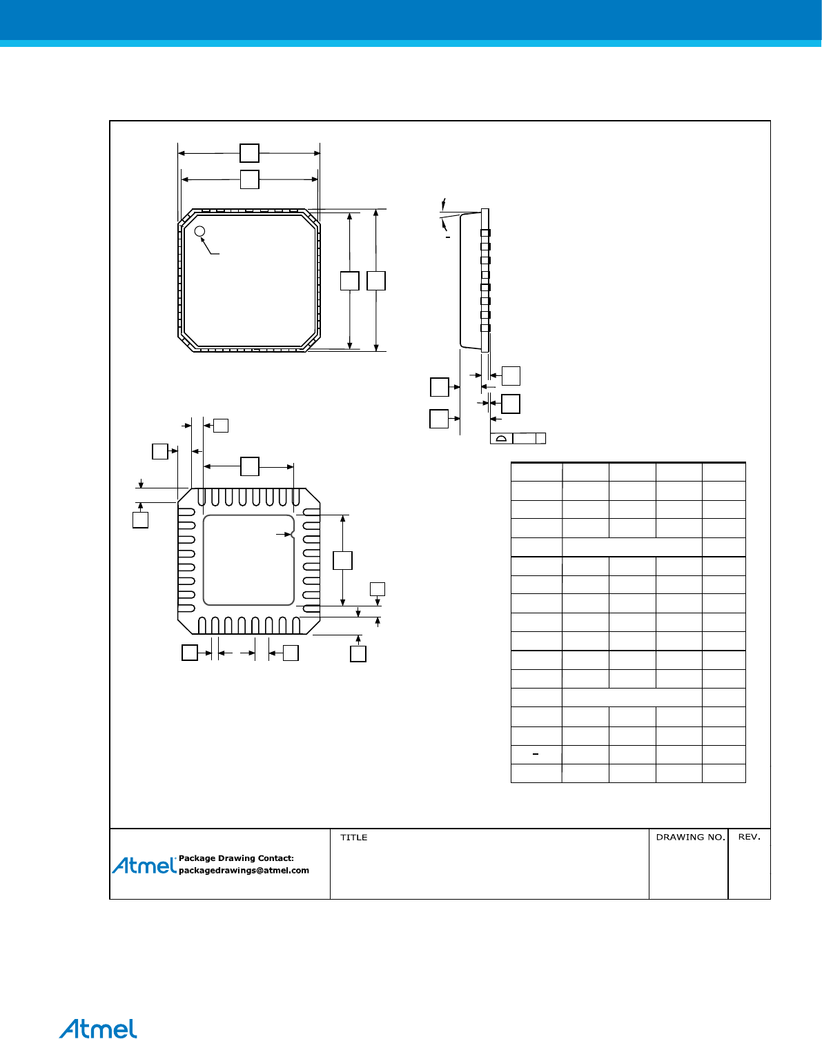
36.3. 32M1-A
COMMON DIMENSIONS
(Unit of Measure = mm)
SYMBOL MIN NOM MAX NOTE
D1
D
E1 E
e
b
A3
A2
A1
A
D2
E2
0.08 C
L
1
2
3
P
P
0
1
2
3
A 0.80 0.90 1.00
A1 – 0.02 0.05
A2 – 0.65 1.00
A3 0.20 REF
b 0.18 0.23 0.30
D
D1
D2 2.95 3.10 3.25
4.90 5.00 5.10
4.70 4.75 4.80
4.70 4.75 4.80
4.90 5.00 5.10
E
E1
E2 2.95 3.10 3.25
e 0.50 BSC
L 0.30 0.40 0.50
P – – 0.60
– – 12o
Note : JEDEC Standard MO-220, Fig . 2 (Anvil Singulation), VHHD-2 .
TOP VIEW
SIDE VIEW
BOTTOM VIEW
0
Pin 1 ID
Pin #1 Notch
(0.20 R)
K 0.20 – –
K
K
32M1-A , 32-pad, 5 x 5 x 1.0mm Bod y, Lead Pitch 0.50mm ,
3.10mm Exposed P ad, Micro Lead Frame P a ckage (MLF) 32M1-A
03/14/2014
F
Atmel ATmega8A [DATASHEET]
Atmel-8159F-8-bit AVR Microcontroller_Datasheet_Complete-09/2015
389

37. Errata
The revision letter in this section refers to the revision of the ATmega8A device.
37.1. ATmega8A, rev. L
•First Analog Comparator conversion may be delayed
•Interrupts may be lost when writing the timer registers in the asynchronous timer
•Signature may be Erased in Serial Programming Mode
•CKOPT Does not Enable Internal Capacitors on XTALn/TOSCn Pins when 32kHz Oscillator is
Used to Clock the Asynchronous Timer/Counter2
•Reading EEPROM by using ST or STS to set EERE bit triggers unexpected interrupt request
1. First Analog Comparator conversion may be delayed
If the device is powered by a slow rising VCC, the first Analog Comparator conversion will take
longer than expected on some devices.
Problem Fix / Workaround:
When the device has been powered or reset, disable then enable theAnalog Comparator before the
first conversion.
2. Interrupts may be lost when writing the timer registers in the asynchronous timer
The interrupt will be lost if a timer register that is synchronous timer clock is written when the
asynchronous Timer/Counter register (TCNTx) is 0x00.
Problem Fix / Workaround:
Always check that the asynchronous Timer/Counter register neither have the value 0xFF nor 0x00
before writing to the asynchronous Timer Control Register (TCCRx), asynchronous Timer Counter
Register (TCNTx), or asynchronous Output Compare Register (OCRx).
3. Signature may be Erased in Serial Programming Mode
If the signature bytes are read before a chiperase command is completed, the signature may be
erased causing the device ID and calibration bytes to disappear. This is critical, especially, if the
part is running on internal RC oscillator.
Problem Fix / Workaround:
Ensure that the chiperase command has exceeded before applying the next command.
4. CKOPT Does not Enable Internal Capacitors on XTALn/TOSCn Pins when 32kHz Oscillator is
Used to Clock the Asynchronous Timer/Counter2
When the internal RC Oscillator is used as the main clock source, it is possible to run the Timer/
Counter2 asynchronously by connecting a 32kHz Oscillator between XTAL1/TOSC1 and XTAL2/
TOSC2. But when the internal RC Oscillator is selected as the main clock source, the CKOPT Fuse
does not control the internal capacitors on XTAL1/TOSC1 and XTAL2/TOSC2. As long as there are
no capacitors connected to XTAL1/TOSC1 and XTAL2/TOSC2, safe operation of the Oscillator is
not guaranteed.
Problem Fix / Workaround:
Use external capacitors in the range of 20 - 36 pF on XTAL1/TOSC1 and XTAL2/TOSC2. This will
be fixed in ATmega8A Rev. G where the CKOPT Fuse will control internal capacitors also when
internal RC Oscillator is selected as main clock source. For ATmega8A Rev. G, CKOPT = 0
(programmed) will enable the internal capacitors on XTAL1 and XTAL2. Customers who want
Atmel ATmega8A [DATASHEET]
Atmel-8159F-8-bit AVR Microcontroller_Datasheet_Complete-09/2015
390

compatibility between Rev. G and older revisions, must ensure that CKOPT is unprogrammed
(CKOPT = 1).
5. Reading EEPROM by using ST or STS to set EERE bit triggers unexpected interrupt request.
Reading EEPROM by using the ST or STS command to set the EERE bit in the EECR register
triggers an unexpected EEPROM interrupt request.
Problem Fix / Workaround:
Always use OUT or SBI to set EERE in EECR.
Atmel ATmega8A [DATASHEET]
Atmel-8159F-8-bit AVR Microcontroller_Datasheet_Complete-09/2015
391

38. Datasheet Revision History
Please note that the referring page numbers in this section are referred to this document. The referring
revision in this section refers to the document revision.
38.1. Rev.8159F – 07/2015
1. New workflow used for the publication.
38.2. Rev.8159E – 02/2013
1. Applied the Atmel new page layout for datasheets including new logo and last page.
2. Removed the reference to the debuggers and In-Circuit Emulators.
3. Added Capacitive touch sensing.
4. Added Electrical Characteristics – TA = -40°C to 105°C.
5. Added Typical Characteristics – TA = -40°C to 105°C.
38.3. Rev.8159D – 02/11
1. Updated the datasheet according to the Atmel new Brand Style Guide.
2. Updated Performing Page Erase by SPM by adding an extra note.
3. Updated Ordering Information to include Tape & Reel.
38.4. DRH_Rev.8159C – 07/09
1. Updated Errata.
38.5. Rev.8159B – 05/09
1. Updated System and Reset Characteristics with new BODLEVEL values
2. Updated ADC Characteristics with new VINT values.
3. Updated Typical Characteristics – TA = -40°C to 85°C view.
4. Updated Errata. ATmega8A, rev L.
5. Created a new Table Of Contents.
38.6. Rev.8159A – 08/08
1. Initial revision (Based on the ATmega8/L datasheet 2486T-AVR-05/08)
2. Changes done compared to ATmega8/L datasheet 2486T-AVR-05/08:
–All Electrical Characteristics are moved to Electrical Characteristics – TA = -40°C to 85°C.
–Updated DC Characteristics with new VOL Max (0.9V and 0.6V) and typical value for ICC.
–Added Speed Grades.
–Added a new sub section System and Reset Characteristics.
–Updated System and Reset Characteristics with new VBOT BODLEVEL = 0 (3.6V, 4.0V and
4.2V).
Atmel ATmega8A [DATASHEET]
Atmel-8159F-8-bit AVR Microcontroller_Datasheet_Complete-09/2015
392


Atmel Corporation 1600 Technology Drive, San Jose, CA 95110 USA T: (+1)(408) 441.0311 F: (+1)(408) 436.4200 | www.atmel.com
© 2015 Atmel Corporation. / Rev.: Atmel-8159F-8-bit AVR Microcontroller_Datasheet_Complete-09/2015
Atmel®, Atmel logo and combinations thereof, Enabling Unlimited Possibilities®, AVR®, and others are registered trademarks or trademarks of Atmel Corporation in
U.S. and other countries. Other terms and product names may be trademarks of others.
DISCLAIMER: The information in this document is provided in connection with Atmel products. No license, express or implied, by estoppel or otherwise, to any
intellectual property right is granted by this document or in connection with the sale of Atmel products. EXCEPT AS SET FORTH IN THE ATMEL TERMS AND
CONDITIONS OF SALES LOCATED ON THE ATMEL WEBSITE, ATMEL ASSUMES NO LIABILITY WHATSOEVER AND DISCLAIMS ANY EXPRESS, IMPLIED
OR STATUTORY WARRANTY RELATING TO ITS PRODUCTS INCLUDING, BUT NOT LIMITED TO, THE IMPLIED WARRANTY OF MERCHANTABILITY,
FITNESS FOR A PARTICULAR PURPOSE, OR NON-INFRINGEMENT. IN NO EVENT SHALL ATMEL BE LIABLE FOR ANY DIRECT, INDIRECT,
CONSEQUENTIAL, PUNITIVE, SPECIAL OR INCIDENTAL DAMAGES (INCLUDING, WITHOUT LIMITATION, DAMAGES FOR LOSS AND PROFITS, BUSINESS
INTERRUPTION, OR LOSS OF INFORMATION) ARISING OUT OF THE USE OR INABILITY TO USE THIS DOCUMENT, EVEN IF ATMEL HAS BEEN ADVISED
OF THE POSSIBILITY OF SUCH DAMAGES. Atmel makes no representations or warranties with respect to the accuracy or completeness of the contents of this
document and reserves the right to make changes to specifications and products descriptions at any time without notice. Atmel does not make any commitment to
update the information contained herein. Unless specifically provided otherwise, Atmel products are not suitable for, and shall not be used in, automotive
applications. Atmel products are not intended, authorized, or warranted for use as components in applications intended to support or sustain life.
SAFETY-CRITICAL, MILITARY, AND AUTOMOTIVE APPLICATIONS DISCLAIMER: Atmel products are not designed for and will not be used in connection with any
applications where the failure of such products would reasonably be expected to result in significant personal injury or death (“Safety-Critical Applications”) without
an Atmel officer's specific written consent. Safety-Critical Applications include, without limitation, life support devices and systems, equipment or systems for the
operation of nuclear facilities and weapons systems. Atmel products are not designed nor intended for use in military or aerospace applications or environments
unless specifically designated by Atmel as military-grade. Atmel products are not designed nor intended for use in automotive applications unless specifically
designated by Atmel as automotive-grade.
