ZedBoard_HW_Users_Guide Zed Board User's Guide
User Manual: Pdf
Open the PDF directly: View PDF ![]() .
.
Page Count: 38
- 1 Introduction
- 2 Functional Description
- 3 Zynq-7000 AP SoC Banks
- 4 Jumper Settings
- 5 Mechanical
- 6 Revision History
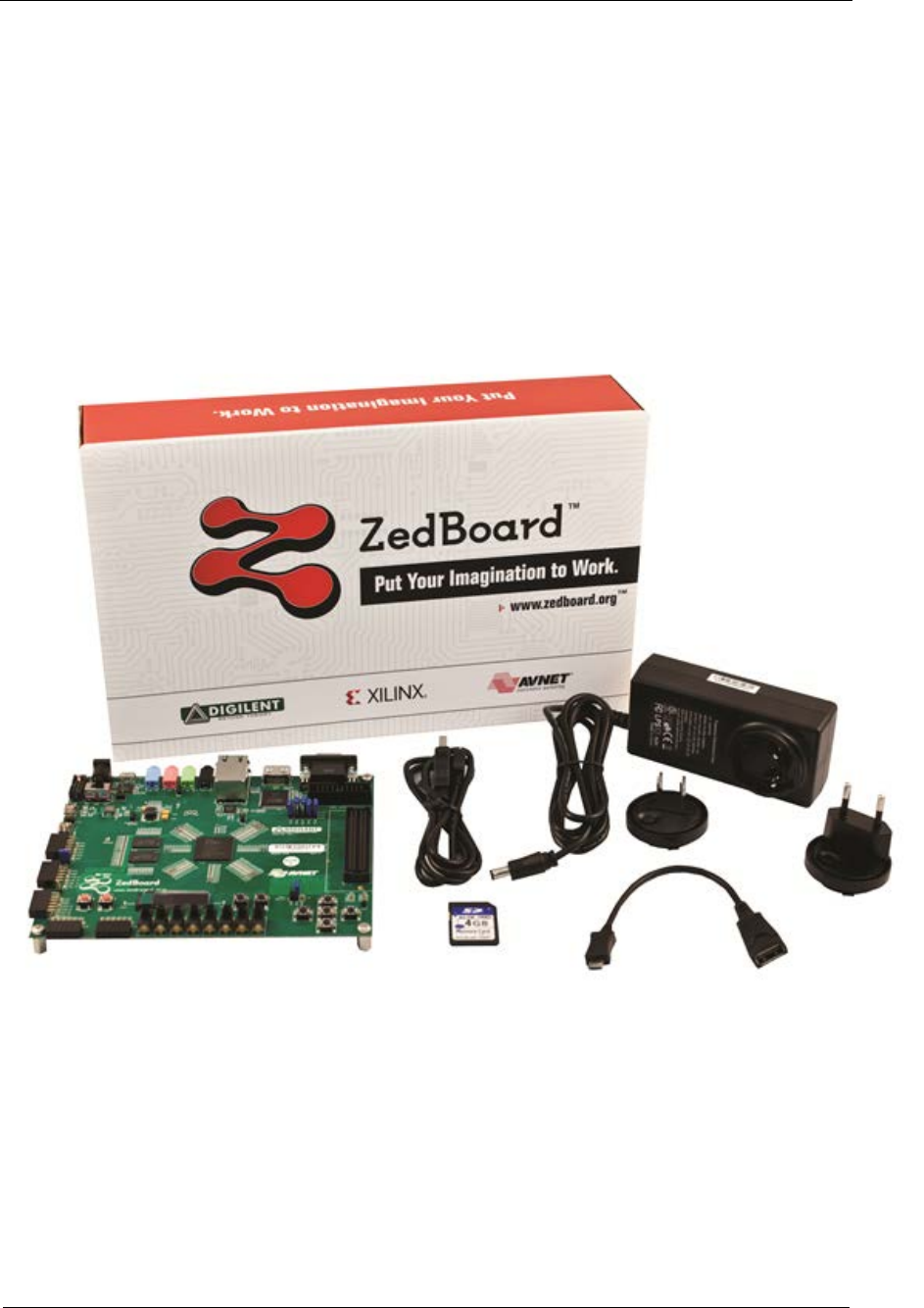
ZedBoard
(Zynq™ Evaluation and Development)
Hardware User’s Guide
Version 2.2
27 January 2014

Table of Contents
1 INTRODUCTION .................................................................................................................................. 2
1.1 ZYNQ BANK PIN ASSIGNMENTS ...................................................................................................... 4
2 FUNCTIONAL DESCRIPTION ............................................................................................................ 5
2.1 ALL PROGRAMMABLE SOC ............................................................................................................. 5
2.2 MEMORY ......................................................................................................................................... 5
2.2.1 DDR3 ...................................................................................................................................... 5
2.2.2 SPI Flash ................................................................................................................................ 7
2.2.3 SD Card Interface ..................................................................................................................10
2.3 USB ...............................................................................................................................................11
2.3.1 USB OTG ...............................................................................................................................11
2.3.2 USB-to-UART Bridge ............................................................................................................11
2.3.3 USB-JTAG .............................................................................................................................12
2.3.4 USB circuit protection ...........................................................................................................13
2.4 DISPLAY AND AUDIO ......................................................................................................................13
2.4.1 HDMI Output .........................................................................................................................13
2.4.2 VGA Connector......................................................................................................................16
2.4.3 I2S Audio Codec ....................................................................................................................17
2.4.4 OLED .....................................................................................................................................18
2.5 CLOCK SOURCES .............................................................................................................................18
2.6 RESET SOURCES .............................................................................................................................18
2.6.1 Power
‐
on Reset (PS_POR_B) ................................................................................................18
2.6.2 Program Push Button Switch .................................................................................................19
2.6.3 Processor Subsystem Reset ....................................................................................................19
2.7 USER I/O ........................................................................................................................................19
2.7.1 User Push Buttons .................................................................................................................19
2.7.2 User DIP Switches .................................................................................................................19
2.7.3 User LEDs .............................................................................................................................20
2.8 10/100/1000 ETHERNET PHY ........................................................................................................20
2.9 EXPANSION HEADERS ....................................................................................................................21
2.9.1 LPC FMC Connector .............................................................................................................21
2.9.2 Digilent Pmod™ Compatible Headers (2x6).........................................................................22
2.9.3 Agile Mixed Signaling (AMS) Connector, J2 .........................................................................23
2.10 CONFIGURATION MODES ................................................................................................................26
2.10.1 JTAG ......................................................................................................................................27
2.11 POWER ...........................................................................................................................................28
2.11.1 Primary Power Input .............................................................................................................28
2.11.2 On/Off Switch ........................................................................................................................28
2.11.3 Regulators ..............................................................................................................................28
2.11.4 Sequencing .............................................................................................................................29
2.11.5 Power Good LED ..................................................................................................................30
2.11.6 Power Estimation ..................................................................................................................30
2.11.7 Testing ...................................................................................................................................31
2.11.8 Probes ....................................................................................................................................31
3 ZYNQ-7000 AP SOC BANKS .............................................................................................................32
3.1 ZYNQ-7000 AP SOC BANK VOLTAGES ..........................................................................................33
4 JUMPER SETTINGS ............................................................................................................................34
5 MECHANICAL ....................................................................................................................................36
6 REVISION HISTORY ..........................................................................................................................37
27-Jan-2014
1

1 Introduction
The ZedBoard is an evaluation and development board based on the Xilinx ZynqTM-7000 All
Programmable SoC (AP SoC). Combining a dual Corex-A9 Processing System (PS) with 85,000
Series-7 Programmable Logic (PL) cells, the Zynq-7000 AP SoC can be targeted for broad use in
many applications. The ZedBoard’s robust mix of on-board peripherals and expansion
capabilities make it an ideal platform for both novice and experienced designers. The features
provided by the ZedBoard consist of:
• Xilinx® XC7Z020-1CLG484C Zynq-7000 AP SoC
o Primary configuration = QSPI Flash
o Auxiliary configuration options
Cascaded JTAG
SD Card
• Memory
o 512 MB DDR3 (128M x 32)
o 256 Mb QSPI Flash
• Interfaces
o USB-JTAG Programming using Digilent SMT1-equivalent circuit
Accesses PL JTAG
PS JTAG pins connected through PS Pmod
o 10/100/1G Ethernet
o USB OTG 2.0
o SD Card
o USB 2.0 FS USB-UART bridge
o Five Digilent Pmod™ compatible headers (2x6) (1 PS, 4 PL)
o One LPC FMC
o One AMS Header
o Two Reset Buttons (1 PS, 1 PL)
o Seven Push Buttons (2 PS, 5 PL)
o Eight dip/slide switches (PL)
o Nine User LEDs (1 PS, 8 PL)
o DONE LED (PL)
• On-board Oscillators
o 33.333 MHz (PS)
o 100 MHz (PL)
• Display/Audio
o HDMI Output
o VGA (12-bit Color)
o 128x32 OLED Display
o Audio Line-in, Line-out, headphone, microphone
• Power
o On/Off Switch
o 12V @ 5A AC/DC regulator
• Software
o ISE® WebPACK Design Software
o License voucher for ChipScope™ Pro locked to XC7Z020
27-Jan-2014
2
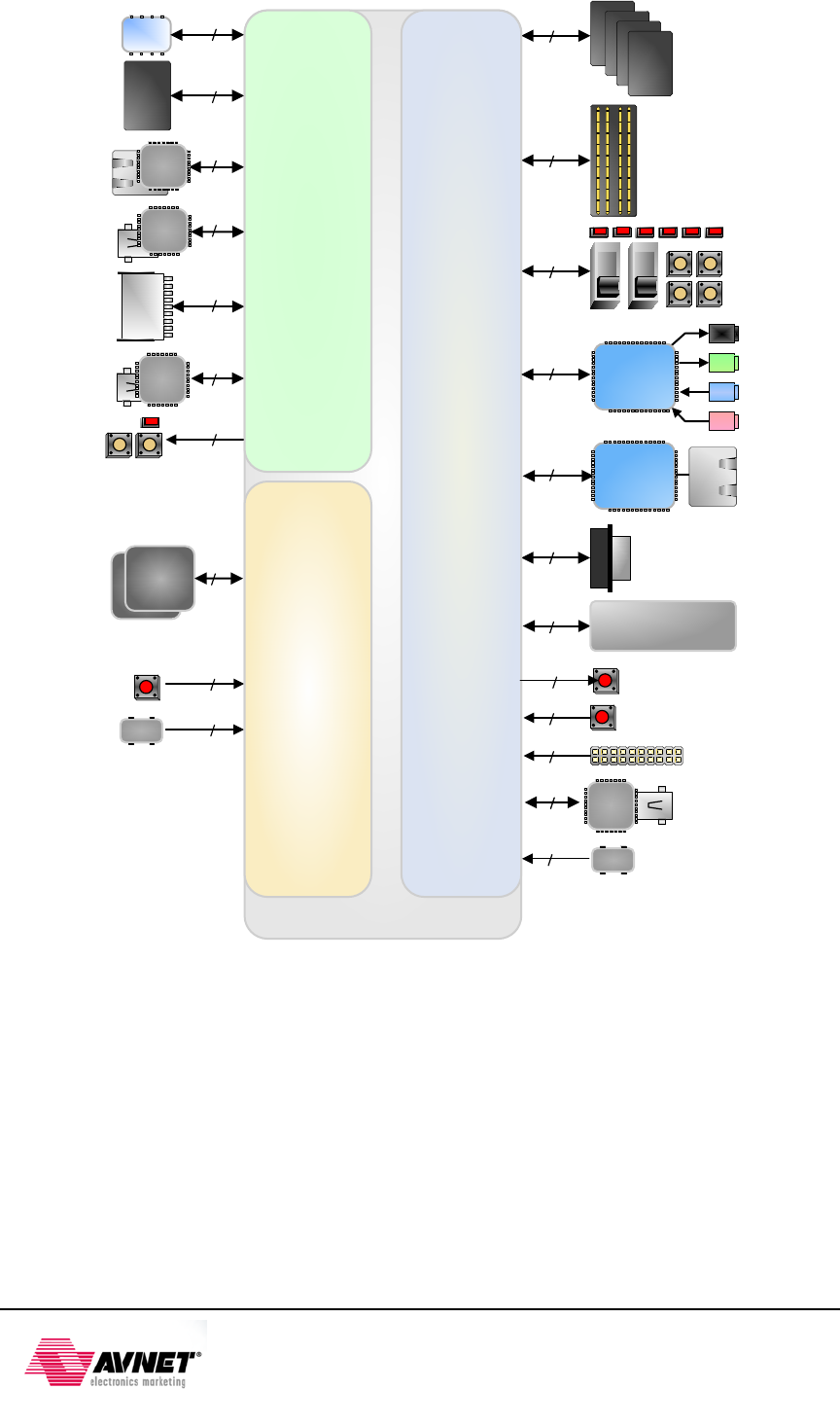
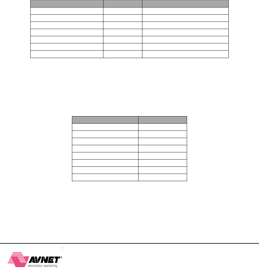
ZYNQ XC7Z020-CLG484
DDR3
MIC In
Line In
Line Out
HdPhn Out
32
Pmods
QSPI
7
Pmod
Flash
8
14
Gbit
Enet
12
USB
OTG
8
SD
2
1 LED,
2 buttons
USB
Cont
USB
UART
3
71
4
USB
Cont
Clk
FMC-LPC
GPIO (8 LEDs,
8 slide switches,
5 pushbuttons)
Type A
HDMI Out
82
21
8
27
10
5
VGA (12-
bit color)
128x32 OLED
PHY
1
1
33Mhz
Reset
Primary JTAG
512Mbyte
DDR3 (x32)
Multiplexed I/O (MIO)Processing System (PS)
Programmable Logic (PL)
1PROG
Display
DDR
PS_RST
JTAG
PS_CLK
<User
Select>
ENET/
MDIO
USBOTG
SD
USBUART
PS_GPIO
QSPI
I2S/ACD
GPIO
FMC
PMOD
HDMI
VGA
OLED
PROG
PHY
HDMI
transmitter
I2S Audio
Codec
XADC
8
GPIO/VP/VN
1DONE LEDDONE
Clk
100Mhz
1
GCLK
Figure 1 – ZedBoard Block Diagram
27-Jan-2014
3
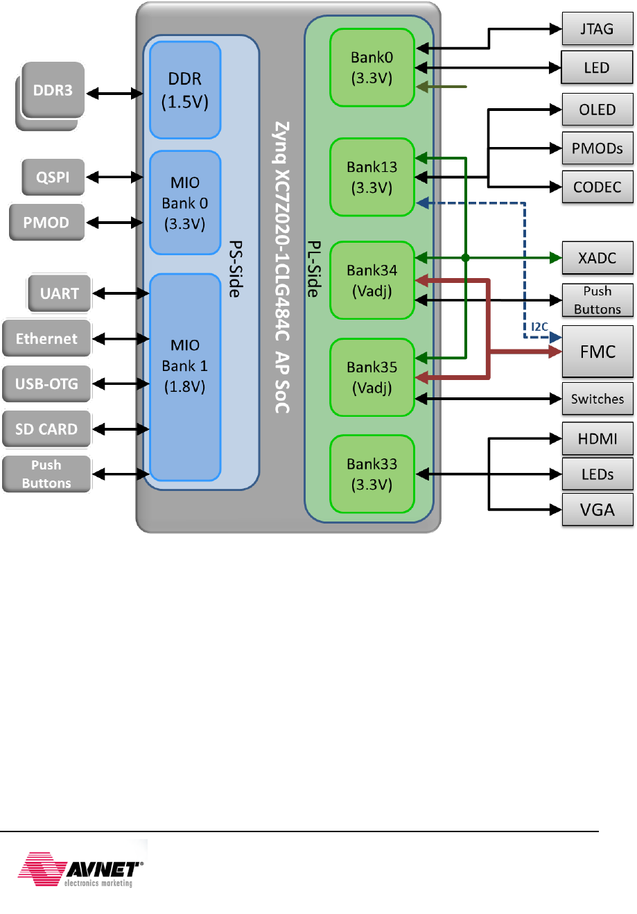
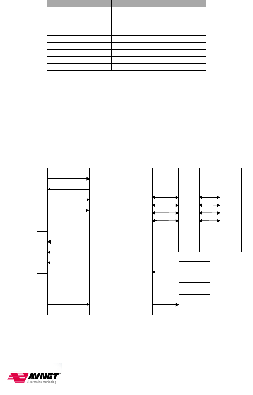
1.1 Zynq Bank Pin Assignments
The following figure shows the Zynq bank pin assignments on the ZedBoard followed by a table
that shows the detailed I/O connections.
Figure 2 - Zynq Z7020 CLG484 Bank Assignments
27-Jan-2014
4

2 Functional Description
2.1 All Programmable SoC
The ZedBoard features a Xilinx Zynq XC7Z020-1CLG484 All Programmable SoC (AP SoC).
Initial ZedBoards were marked ‘Rev C’ and shipped with Engineering Sample "CES" grade
silicon. Later ‘Rev D’ shipments switched to production "C" grade silicon once those became
available. The Zynq-7000 AP SoC part markings indicate the silicon grade.
2.2 Memory
Zynq contains a hardened PS memory interface unit. The memory interface unit includes a
dynamic memory controller and static memory interface modules.
2.2.1 DDR3
The ZedBoard includes two Micron DDR3 128 Megabit x 16 memory components creating a 32-
bit interface, totaling 512 MB.
Earlier ZedBoards used Micron MT41J128M16HA-15E:D, but
As of August 2012, this device has been marked by Micron for end-of-life. There are several
options that Micron offers for a replacement. ZedBoard will likely migrate to the
MT41K128M16JT-125 device, although this is pending validation. The DDR3 is connected to the
hard memory controller in the Processor Subsystem (PS) as outlined in the Zynq datasheet.
The multi-protocol DDR memory controller is configured for 32-bit wide accesses to a 512 MB
address space. The PS incorporates both the DDR controller and the associated PHY, including
its own set of dedicated I/Os. DDR3 memory interface speeds up to 533MHz (1066Mbs) are
supported.
The DDR3 uses 1.5V SSTL-compatible inputs. DDR3 Termination is utilized on the ZedBoard.
The Zynq-7000 AP SoC and DDR3 have been placed close together keeping traces short and
matched.
DDR3 on the PS was routed with 50 ohm targeted trace impedance for single-ended signals, and
DCI resistors (VRP/VRN) as well as differential clocks set to 80 ohms. Each DDR3 chip needs its
own 240-ohm pull-down on ZQ. The Xilinx Zynq-7000 All Programmable SoC PCB Design and
Pin Planning Guide (UG933) recommends using 40 ohm trace impedance for DDR3 single-ended
signals, so designers looking to duplicate the ZedBoard design may want consider this in their
own board design. See the appropriate ZedBoard Errata document for more details.
DDR-VDDQ is set to 1.5V to support the DDR3 devices selected. DDR-VTT is the termination
voltage which is ½ DDR-VDDQ. DDR-VREF is a separate buffered output that is equal to ½
nominal DDR-VDDQ. The DDR-VREF is isolated to provide a cleaner reference for the DDR
level transitions.
27-Jan-2014
5
The PCB design guidelines outlined in Zynq datasheet must be followed for trace matching, etc.
Table 1 - DDR3 Connections
Signal Name
Description
Zynq pin
DDR3 pin
DDR_CK_P
Differential clock
output
N4 J7
DDR_CK_N
Differential clock
output
N5 K7
DDR_CKE
Clock enable
V3
K9
DDR_CS_B
Chip select
P6
L2
DDR_RAS_B
RAS row address
select
R5 J3
DDR_CAS_B
RAS column address
select
P3 K3
DDR_WE_B
Write enable
R4
L3
DDR_BA[2:0]
Bank address
PS_DDR_BA[2:0]
BA[2:0]
DDR_A[14:0]
Address
PS_DDR_A[14:0]
A[14:0]
DDR_ODT
Output dynamic
termination
P5 K1
DDR_RESET_B
Reset
F3
T2
DDR_DQ[31:0]
I/O Data
PS_DDR_[31:0]
DDR3_DQ pins
DDR_DM[3:0]
Data mask
PS_DDR_DM[3:0]
LDM/UDM x2
DDR_DQS_P[3:0]
I/O Differential data
strobe
PS_DDR_DQS_P[3:0] UDQS/LDQS
DDR_DQS_N[3:0]
I/O Differential data
strobe
PS_DDR_DQS_N[3:0] UDQS#/LDQS#
DDR_VRP
I/O Used to calibrate
input termination
N7 N/A
DDR_VRN
I/O Used to calibrate
input termination
M7 N/A
DDR_VREF[1:0]
I/O Reference
voltage
H7, P7 H1
For best DDR3 performance, DRAM training is enabled for write leveling, read gate, and read
data eye options in the PS Configuration Tool in Xilinx Platform Studio (XPS) or the IP Editor in
Vivado. Two entries allow for DQS to Clock Delay and Board Delay information to be specified for
each of the four byte lanes. The tools will calculate these board training details based upon
specific trace lengths for certain DDR3 signals.
The PCB lengths are contained in the ZedBoard PCB trace length reports. The DQS to CLK
Delay and Board Delay values are calculated specific to the ZedBoard memory interface PCB
design. The Xilinx tools allow for up to 4 memory devices to be configured for DDR3 4x8 flyby
topology. Note that ZedBoard is configured for DDR3 2x16 flyby routing topology. The first two
clock trace midpoint values (CLK0 and CLK1) are used to represent the Micron device electrically
furthest from the 7Z020 (IC25) and the second two clock trace midpoint values (CLK2 and CLK3)
are used to represent the Micron device electrically closest to the 7Z020 (IC26). The worksheet
calculation results are shown in the following table.
27-Jan-2014
6
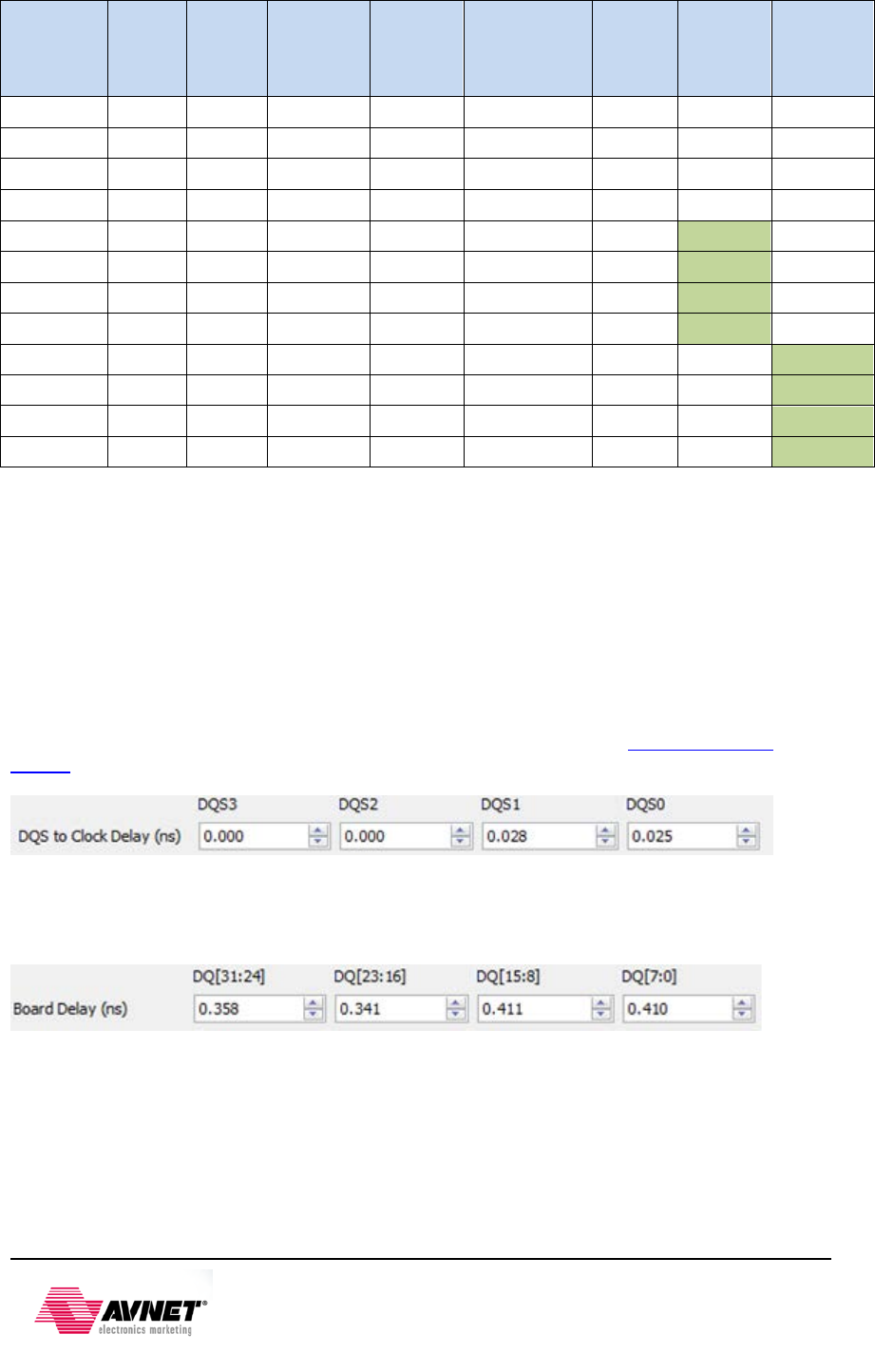
Table 2 - DDR3 Worksheet Calculations
Pin Group
Length
(mm)
Length
(mils)
Package
Length
(mils)
Total
Length
(mils)
Propagation
Delay
(ps/inch)
Total
Delay
(ns)
DQS to
CLK
Delay
(ns)
Board
Delay
(ns)
CLK0 55.77 2195.9 470 2665.9 160 0.427
CLK1 55.77 2195.9 470 2665.9 160 0.427
CLK2 41.43 1631.1 470 2101.1 160 0.336
CLK3 41.43 1631.1 470 2101.1 160 0.336
DQS0 51.00 2008.0 504 2512.0 160 0.402
0.025
DQS1 50.77 1998.8 495 2493.8 160 0.399 0.028
DQS2 41.59 1637.6 520 2157.6 160 0.345 -0.009
DQS3 41.90 1649.4 835 2484.4 160 0.398 -0.061
DQ[7:0] 50.63 1993.3 465 2458.3 160 0.393
0.410
DQ[15:8] 50.71 1996.4 480 2476.4 160 0.396
0.411
DQ[23:16] 40.89 1609.9 550 2159.9 160 0.346
0.341
DQ[31:24] 40.58 1597.8 780 2377.8 160 0.380
0.358
The DQS to CLK Delay fields in the PS7 DDR Configuration window should be populated using
the corresponding values from the previous table.
The configuration fields of the tool may not allow you to input a negative delay value, this is a
known problem with the 14.1 tools and scheduled for correction in the 14.2 tools release. In the
case of DQS2 and DQS3 fields for DQS to CLK Delay, simply enter a value of zero rather than
the negative delay values. This is an acceptable workaround since the calculated values are
relatively close to zero and the values provided in these fields are used as initial values for the
read/write training for DDR3. Keep in mind for LPDDR2 there is no write leveling, and for DDR2
there is no training whatsoever. In these memory use cases, the accuracy of the trace length info
is more important. This is covered in further detail in section 10.6.8 of the Xilinx Zynq TRM,
UG585.
Figure 3 - DQS to Clock Delay Settings
The Board Delay fields in the PS7 DDR Configuration window should be populated using the
corresponding values from the table above.
Figure 4 - DDR3 Board Delay Settings
2.2.2 SPI Flash
The ZedBoard features a 4-bit SPI (quad-SPI) serial NOR flash. The Spansion S25FL256S is
used on this board. The Multi-I/O SPI Flash memory is used to provide non-volatile code, and
data storage. It can be used to initialize the PS subsystem as well as configure the PL
subsystem (bitstream). Spansion provides Spansion Flash File System (FFS) for use after
booting the Zynq-7000 AP SoC.
27-Jan-2014
7
The relevant device attributes are:
• 256Mbit
• x1, x2, and x4 support
• Speeds up to 104 MHz, supporting Zynq configuration rates @ 100 MHz
o In Quad-SPI mode, this translates to 400Mbs
• Powered from 3.3V
The SPI Flash connects to the Zynq-7000 AP SoC supporting up to Quad-I/O SPI interface. This
requires connection to specific pins in MIO Bank 0/500, specifically MIO[1:6,8] as outlined in the
Zynq datasheet. Quad-SPI feedback mode is used, thus qspi_sclk_fb_out/MIO[8] is connected to
a 20K pull-up resistor to 3.3V. This allows a QSPI clock frequency greater than FQSPICLK2.
Note: Zynq only supports 24-bit addressing, however the full capacity of the 256Mb Flash can be
accessed via internal bank switching. As of now the S25FL256S is not supported in iMPACT.
Note: 14.x is required for in-direct QSPI Flash Programming.
Table 3 – QSPI Flash Pin Assignment and Definitions
Signal Name Description
Zynq Pin
MIO
QSPI Pin
DQ0
Data0
A2 (Bank MIO0/500)
1:6
5
DQ1
Data1
F6 (MIO Bank 0/500)
2
DQ2
Data2
E4 (MIO Bank 0/500)
3
DQ3
Data3
A3 (MIO Bank 0/500)
7
SCK
Serial Data Clock
A4 (MIO Bank 0/500)
6
CS
Chip Select
A1 (MIO Bank 0/500)
1
FB Clock
QSPI Feedback
E5 (MIO Bank 0/500)
8
N/C
Note: The QSPI data and clock pins are shared with the Boot Mode jumpers.
27-Jan-2014
8
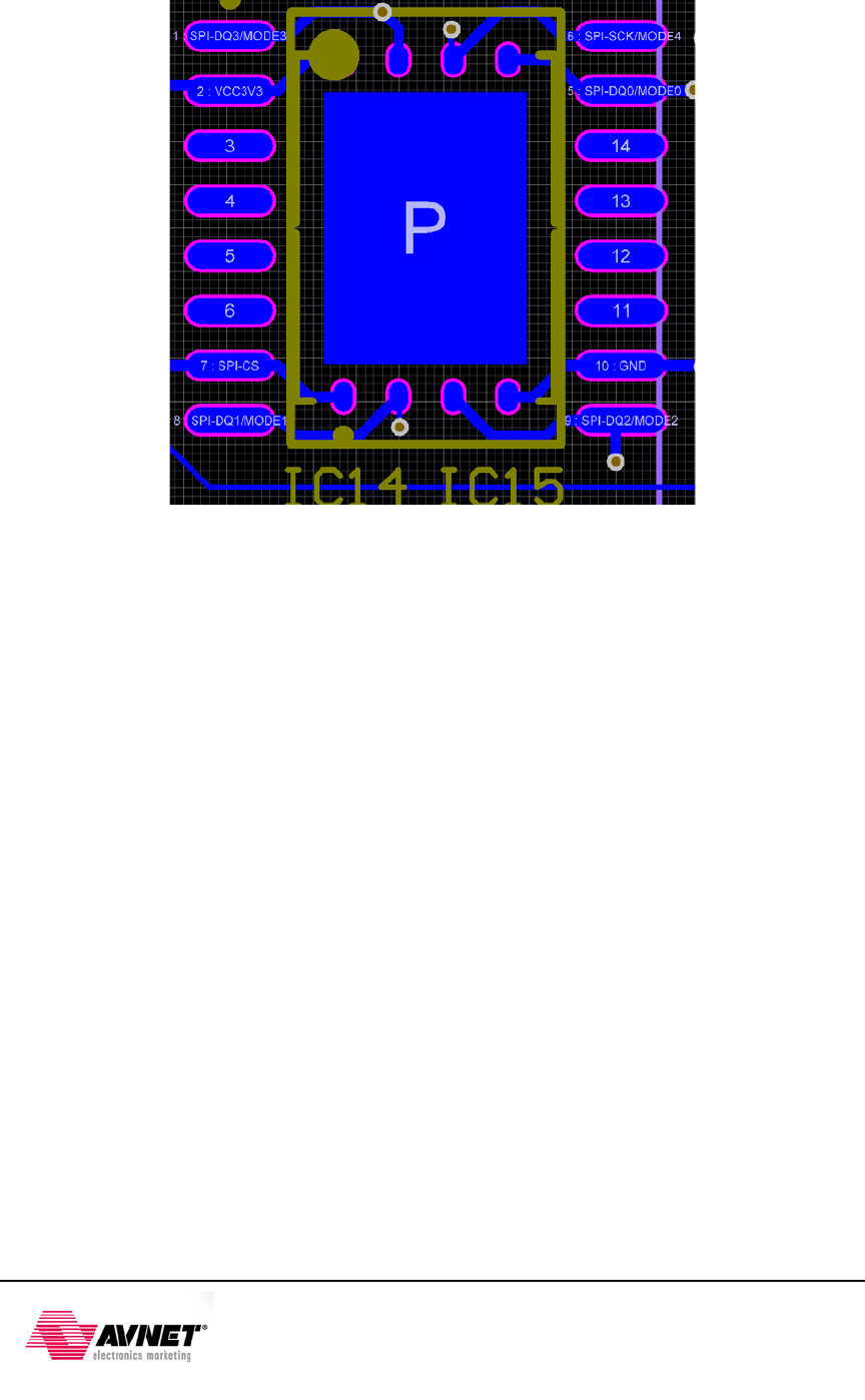
Two packages can be used on the ZedBoard; SO-16 and WSON. For the WSON package,
there is a heat sink slug under the package that is not connected to any signal on the PCB.
Figure 5 - Overlying Packages for SPI Flash
27-Jan-2014
9
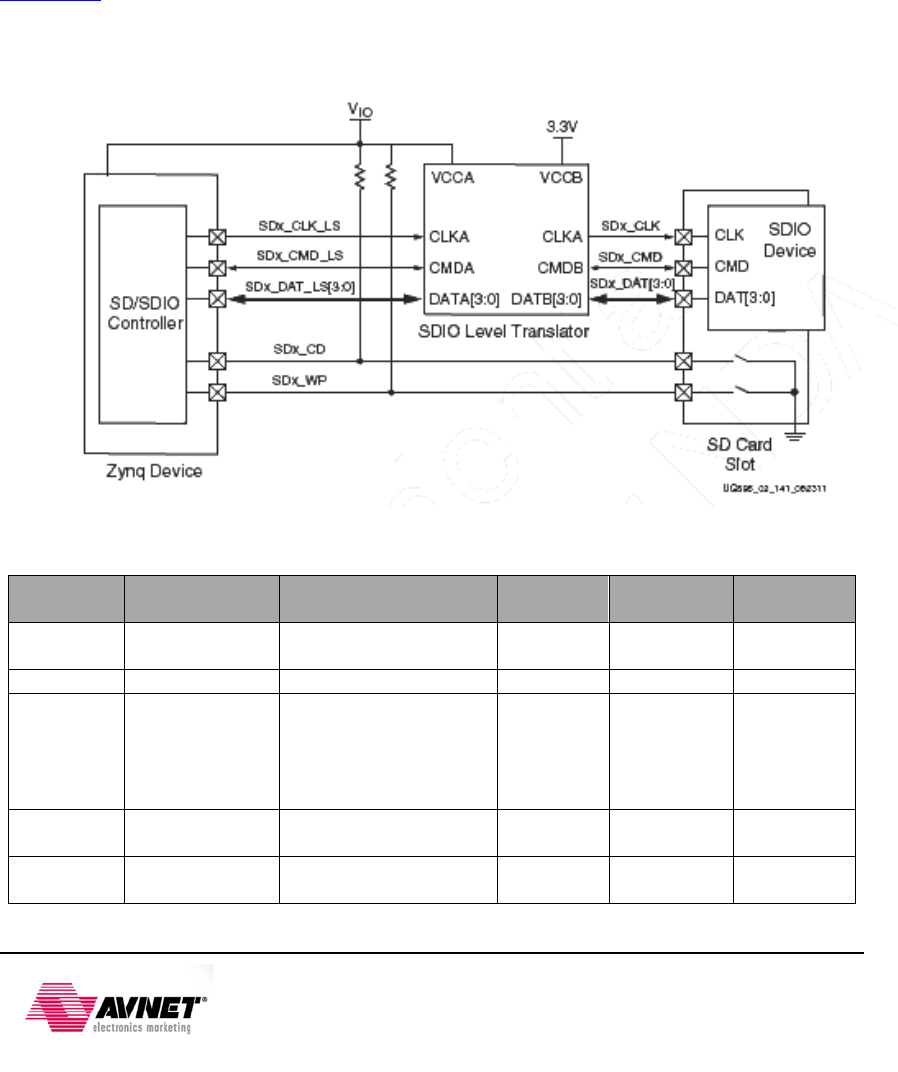
2.2.3 SD Card Interface
The Zynq PS SD/SDIO peripheral controls communication with the ZedBoard SD Card (A 4GB
Class 4 card is included in the ZedBoard kit.) The SD card can be used for non-volatile external
memory storage as well as booting the Zynq-7000 AP SoC. PS peripheral sd0 is connected
through Bank 1/501 MIO[40-47], including, Card Detect and Write Protect.
The SD Card is a 3.3V interface but is connected through MIO Bank 1/501 (1.8V). Therefore, a
TI TXS02612 level shifter performs this translation. The TXS02612 is a 2-port SDIO port
expander with level translation. ZedBoard only makes use of one of these parts. TI offered an
alternative TXS0206 device, but the 0.4mm pitch of that device’s packaging was too fine for our
manufacturer.
Based on the Zynq TRM, host mode is the only mode supported.
The ZedBoard SD Card is connected through a 9-pin standard SD card connector, J12, TE
2041021-1. A Class 4 card or better is recommended.
Note: To use the SD Card, JP6 must be shorted.
Figure 6 - SD Card Interface
Table 4 – SD Card Pin Assignment and Definitions
Signal
Name
Description Zynq Pin
MIO
Level Shift
Pin
SD Card
Pin
CLK Clock
E14 (MIO Bank
1/501)
40 Pass-Thru 5
CMD
Command
C8 ((MIO Bank 1/501)
41
Pass-Thru
2
Data[3:0] Data
MIO Bank 1/501
D0: D8
D1: B11
D2: E13
D3: B9
42:45 Pass-Thru
Data Pins
7
8
9
1
CD Card Detect
B10 (MIO Bank
1/501)
47 Pass-Thru CD
WP Write Protect
D12 ((MIO Bank
1/501)
46 Pass-Thru WP
27-Jan-2014
10
2.3 USB
2.3.1 USB OTG
Warning: After the design of the ZedBoard was complete, a timing incompatibility
between the TUSB1210 PHY and Zynq was discovered. The TUSB1210 is not
recommended for new designs with Xilinx Zynq. Please refer to the ZedBoard Errata for
more details.
ZedBoard implements one of the two available PS USB OTG interfaces. An external PHY with
an 8-bit ULPI interface is required. A TI TUSB1210 Standalone USB Transceiver Chip is used as
the PHY. The PHY features a complete HS-USB Physical Front-End supporting speeds of up to
480Mbs. This part is available in a 32-pin QFN package. VCCio for this device is 1.8V and
cannot be connected through level shifters. The PHY is connected to MIO Bank 1/501, which is
powered at 1.8V. Additionally the USB chip must clock the ULPI interface which requires an
oscillator. A Fox XPRESSO oscillator (767-26-31) is used on ZedBoard.
The external USB interface connects through a TE 1981584-1.
The usb0 peripheral is used on the PS, connected through MIO[28-39] in MIO Bank 1/501.
This USB port will not power the board. However, ZedBoard provides 5V when in Host or OTG
modes. REFCLK pin of TUSB1210 is tied to ground as the Zynq-7000 AP SoC will drive the
CLOCK input of this part.
Table 5 - USB OTG Pin Assignment and Definitions
Signal Name Description Zynq Pin
MIO
TUSB1210
Pin
USB
Conn Pin
OTG_Data[8:0]
USB Data lines
MIO Bank 1/501
28:39
Data[7:0]
N/C
OTG_CLOCK
USB Clock
MIO Bank 1/501
26
N/C
OTG_DIR
ULPI DIR output signal
MIO Bank 1/501
31
N/C
OTG_STP
ULPI STP input signal
MIO Bank 1/501
29
N/C
OTG_NXT
ULPI NXT output signal
MIO Bank 1/501
2
N/C
OTG_CS
USB Chip Select
11
N/C
DP
DP pin of USB Connector
N/C
18
2
DM
DM pin of USB Connector
N/C
19
3
ID
Identification pin of the
USB connector
N/C 23 4
OTG_RESET_B
Reset
MIO Bank 1/501
27
N/C
OTG_VBUS_OC
VBus Output Control
Bank 34
L16
TPS2051
See the Jumper Settings section for configuring the USB interface for Host, Device and OTG
mode. The jumpers control the Vbus supply as well.
2.3.2 USB-to-UART Bridge
The ZedBoard implements a USB-to-UART bridge connected to a PS UART peripheral. A
Cypress CY7C64225 USB-to-UART Bridge device allows connection to a host computer. The
USB/UART device connects to the USB Micro B connector, J14, (TE 1981584-1) on the board.
Only basic TXD/RXD connection is implemented. If flow control is required this can be added
through Extended MIO on a PL-Pmod™.
Cypress provides royalty-free Virtual COM Port (VCP) drivers which permit the CY7C64225 USB-
to-UART bridge to appear as a COM port to host computer communications application software
(for example, HyperTerm or Tera Term). Please refer to the CY7C64225 Setup Guide posted on
zedboard.org for detailed instructions for installing the driver.
27-Jan-2014
11
The UART 1 Zynq PS peripheral is accessed through MIO[48:49] in MIO Bank 1/501 (1.8V).
Since the CY7C64225 device requires either 3.3V or 5V signaling, a TI TXS0102 level shifter is
used to level shift between 3.3V and 1.8V.
This USB port will not power the board. Therefore, Vbus needs to be connected to 3.3V though a
1KΩ series resistor. The Wake pin, pin 22, connects to GND. A 24Ω series resistor was placed
on each of the data lines, D+ and D-.
Table 6 – CY7C6 Connections
UART
Function in
Zynq
Zynq Pin MIO Schematic Net
Name CY7C6 Pin UART Function
in CY7C64225
TX, data out
D11 (MIO Bank
1/501)
48:49 USB_1_RXD 23 RXD, data in
RX, data in
C14 (MIO Bank
1/501)
USB_1_TXD 4 TXD, data out
Figure 7 – USB-UART Bridge Interface
2.3.3 USB-JTAG
The ZedBoard provides JTAG functionality based on the Digilent USB High Speed JTAG Module,
SMT1 device. This USB-JTAG circuitry is fully supported and integrated into Xilinx ISE tools,
including iMPACT, ChipScope, and SDK Debugger. Designers who want to re-use this circuit on
their board can do so by acquiring these modules from Avnet.
http://www.em.avnet.com/en-us/design/drc/Pages/Digilent-JTAG-SMT1-Surface-Mount-
Programming-Module.aspx
The JTAG is available through a Micro B USB connector, J17, TE 1981568-1. TCK has a series
termination resistor, 20-30Ω, to prevent signal integrity issues.
For the JTAG Chain setup, please refer to the Configuration section.
27-Jan-2014
12
2.3.4 USB circuit protection
All USB data lines, D+/-, are protected with a TE SESD0402Q2UG-0020-090.
Figure 8 – ESD Protection
2.4 Display and Audio
2.4.1 HDMI Output
An Analog Devices ADV7511 HDMI Transmitter provides a digital video interface to the
ZedBoard. This 225MHz transmitter is HDMI 1.4- and DVI 1.0-compatible supporting 1080p60
with 16-bit, YCbCr, 4:2:2 mode color.
The ADV7511 supports both S/PDIF and 8-channel I2S audio. The S/PDIF can carry compressed
audio including Dolby® Digital, DTS®, and THX®. There is an independent DPDIF input and
output. The I2S interface is not connected on ZedBoard. Analog Devices offers Linux drivers
and reference designs illustrating how to interface to this device.
The HMDI Transmitter has 25 connections to Bank 35 (3.3V) of the Zynq-7000 AP SoC:
USB
Con
n
Level
Shifter
D+
D-
27-Jan-2014
13
Table 7 - HDMI Interface Connections
Signal Name
Description
Zynq pin
ADV7511 pin
HDP
Hot Plug Detect signal input
N/C
30
HD-INT
Interrupt signal output
W16
45
HD-SCL
I2C Interface. Supports CMOS
logic levels from 1.8V to 3.3V
AA18
55
HD-SDA
Y16
56
HD-CLK
Video Clock Input. Supports
typical CMOS logic levels from
1.8V up to 3.3V
W18
79
HD-VSYNC
Vertical Sync Input (Not required
if using embedded syncs)
W17
2
HD-HSYNC
Horizontal Sync Input (Not
required if using embedded
syncs)
V17
98
HD-DE
Data Enable signal input for
Digital Video (Not required if
using embedded syncs)
U16
97
HD_D[15:0]
Video Data Input
Bank 35
D0: Y13
D1: AA12
D2: AA14
D3: Y14
D4: AB15
D5: AB16
D6: AA16
D7: AB17
D8: AA17
D9: Y15
D10: W13
D11: W15
D12: V15
D13: U17
D14: V14
D15: V13
88
87
86
85
84
83
82
81
80
78
74
73
72
71
70
69
HD-SPDIF
Sony/Philips Digital Interface
Audio Input
U15
10
HD-SPDIFO
Sony/Philips Digital Interface
Audio Output
Y18
46
27-Jan-2014
14
2.4.2 VGA Connector
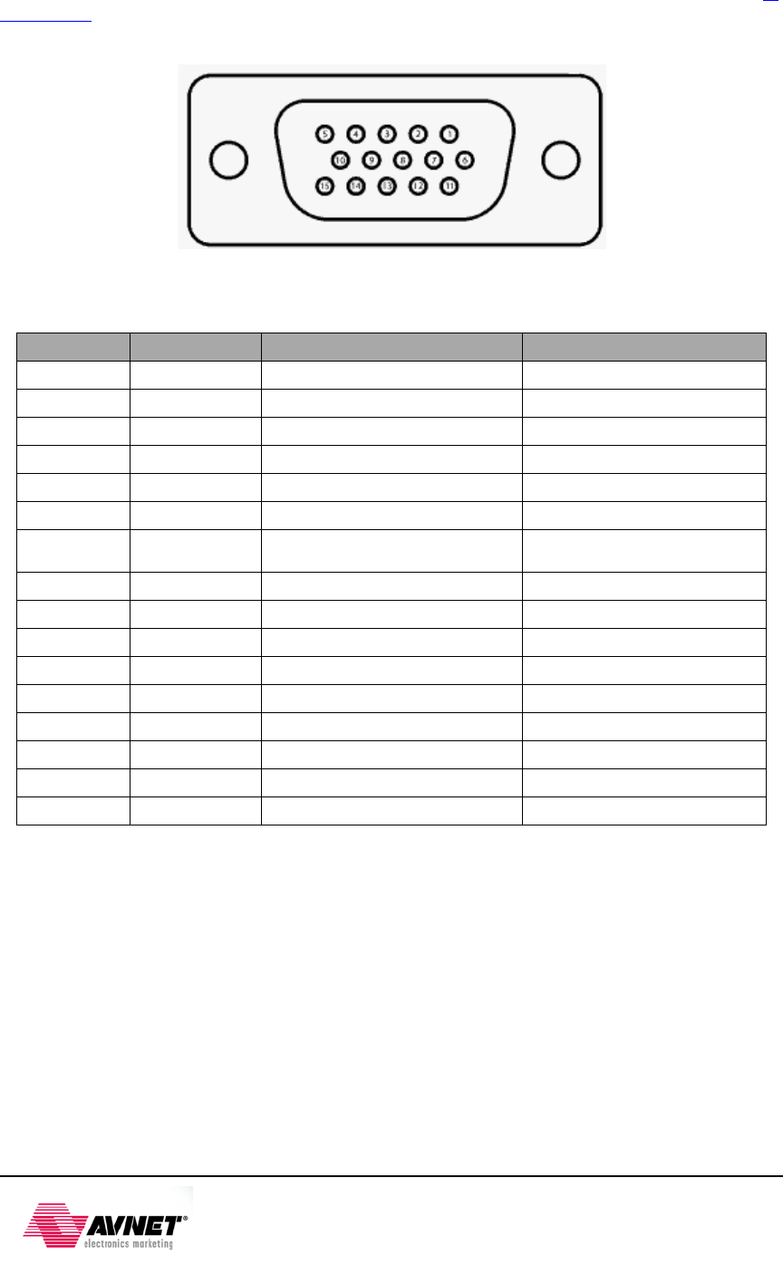
The ZedBoard also allows 12-bit color video output through a through-hole VGA connector, TE 4-
1734682-2. Each color is created from resistor-ladder from four PL pins.
Figure 10 - DB15
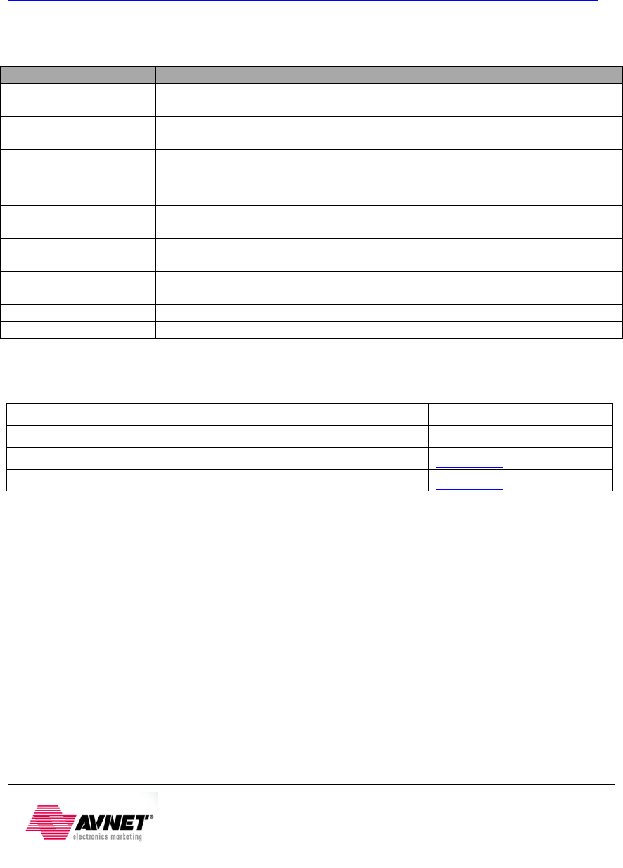
Table 8 - VGA Connections
VGA Pin
Signal
Description
Zynq Pin
1
RED
Red video
V20, U20, V19, V18
2
GREEN
Green video
AB22, AA22, AB21, AA21
3
BLUE
Blue video
Y21, Y20, AB20, AB19
4
ID2/RES
formerly Monitor ID bit 2
NC
5
GND
Ground (HSync)
NC
6
RED_RTN
Red return
NC
7
GREEN_RTN
Green return
NC
8
BLUE_RTN
Blue return
NC
9
KEY/PWR
formerly key
NC
10
GND
Ground (VSync)
NC
11
ID0/RES
formerly Monitor ID bit 0
NC
12
ID1/SDA
formerly Monitor ID bit 1
NC
13
HSync
Horizontal sync
AA19
14
VSync
Vertical sync
Y19
15
ID3/SCL
formerly Monitor ID bit 3
NC
27-Jan-2014
16
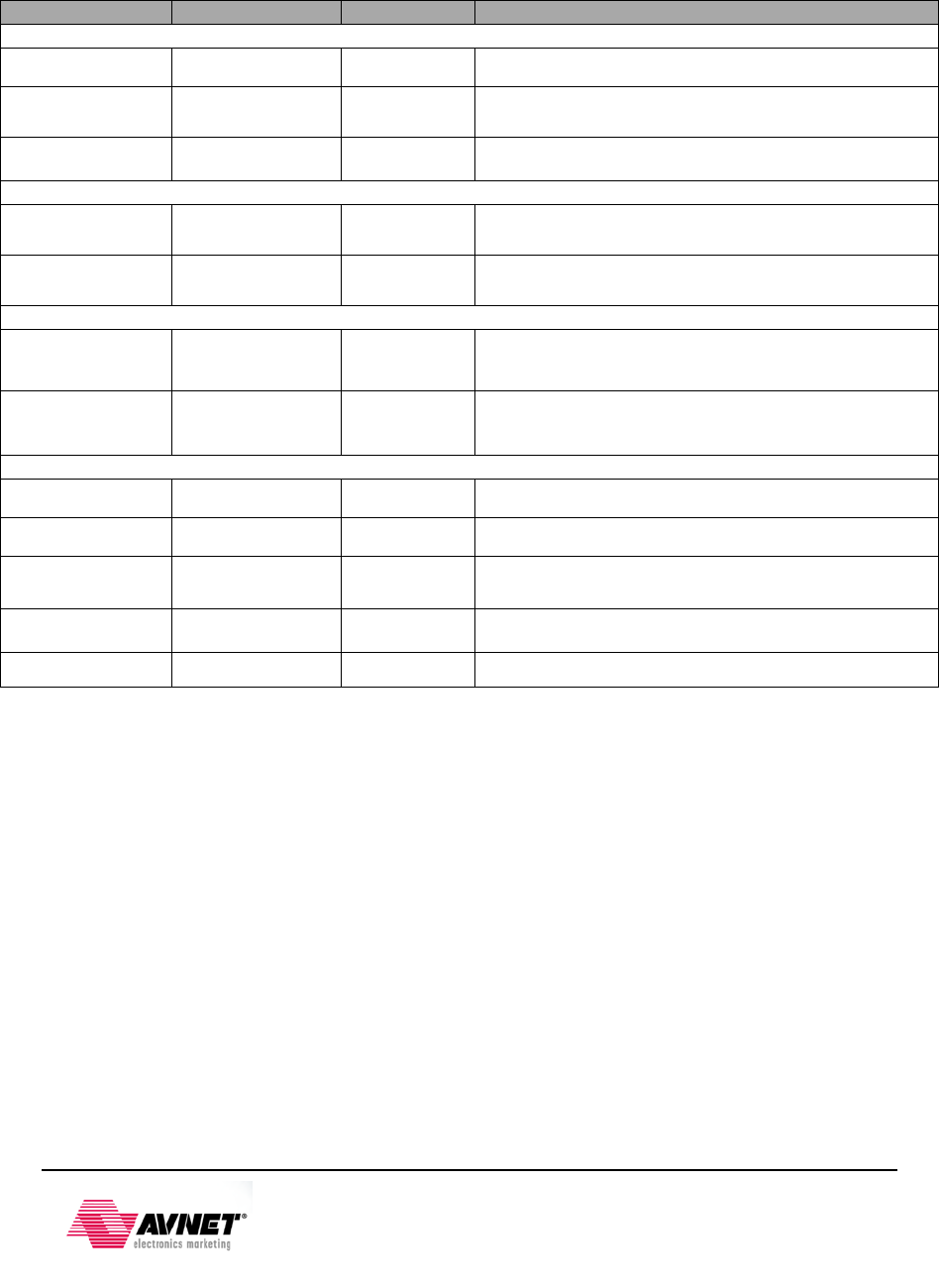
2.4.3 I2S Audio Codec
An Analog Devices ADAU1761 Audio Codec provides integrated digital audio processing to the
Zynq-7000 AP SoC. It allows for stereo 48KHz record and playback. Sample rates from 8KHz to
96KHz are supported. Additionally, the ADAU1761 provides digital volume control. The Codec
can be configured using Analog Devices SigmaStudio™ for optimizing audio for specific
acoustics, numerous filters, algorithms and enhancements. Analog Devices provides Linux
drivers for this device.
http://www.analog.com/en/content/cu_over_sigmastudio_graphical_dev_tool_overview/fca.html
The Codec interface to the Zynq-7000 AP SoC consists of the following connections:
Table 9 - CODEC Connections
Signal Name
Description
Zynq pin
ADAU1761 pin
AC-ADR0
I2C Address Bit 0/SPI Latch
Signal
AB1 3
AC-ADR1
I2C Address Bit 1/SPI Data
Input
Y5 30
AC-MCLK
Master Clock Input
AB2 2
AC-GPIO2
Digital Audio Bit Clock
Input/Output
AA6 28
AC-GPIO3
Digital Audio Left-Right Clock
Input/Output
Y6 29
AC-GPIO0
Digital Audio Serial-Data DAC
Input
Y8 27
AC-GPIO1
Digital Audio Serial Data ADC
Output
AA7 26
AC-SDA
I2C Serial Data interface
AB5
31
AC-SCK
I2C Serial Data interface
AB4
32
The Codec connects to the following connectors:
Table 10 - External Codec Connections
3.5mm Audio (Mic In) Pink
TE
1734152-5
3.5mm Audio (Line In) Light Blue
TE
1734152-6
3.5mm Audio (Line Out) Lime
TE
1734152-4
3.5mm Audio (Headphone) Black
TE
1734152-7
27-Jan-2014
17
2.4.4 OLED
An Inteltronic/Wisechip UG-2832HSWEG04 OLED Display is used on the ZedBoard. This
provides a 128x32 pixel, passive-matrix, monochrome display. The display size is 30mm x
11.5mm x 1.45mm.
Table 11 - OLED Connections
Pin Number
Symbol
Zynq Pin
Function
Power Supply
7 VDD U12 Power Supply for Logic
6 VSS N/C Ground of OEL System
15 VCC N/C Power Supply for OEL Panel
Driver
13 IREF N/C Current Reference for Brightness Adjustment
14 VCOMH N/C Voltage Output High Level for COM Signal
DC/DC Converter
5 VBAT U11 Power Supply for DC/DC Converter Circuit
3 / 4
1 / 2 C1P / C1N
C2P / C2N N/C Positive Terminal of the Flying Inverting Capacitor
Negative Terminal of the Flying Boost Capacitor
Interface
9 RES# U9 Power Reset for Controller and Driver
8 CS# N/C Chip Select – Pulled Down on Board
10 D/C# U10 Data/Command Control
11 SCLK AB12 Serial Clock Input Signal
12 SDIN AA12 Serial Data Input Signal
2.5 Clock sources
The Zynq-7000 AP SoC’s PS subsystem uses a dedicated 33.3333 MHz clock source, IC18, Fox
767-33.333333-12, with series termination. The PS infrastructure can generate up to four PLL-
based clocks for the PL system. An on-board 100 MHz oscillator, IC17, Fox 767-100-136,
supplies the PL subsystem clock input on bank 13, pin Y9.
2.6 Reset Sources
2.6.1 Power
‐
on Reset (PS_POR_B)
The Zynq PS supports external power-on reset signals. The power-on reset is the master reset of
the entire chip. This signal resets every register in the device capable of being reset. ZedBoard
drives this signal from a comparator that holds the system in reset until all power supplies are
valid. Several other IC’s on ZedBoard are reset by this signal as well.
27-Jan-2014
18
2.6.2 Program Push Button Switch
A PROG push switch, BTN6, toggles Zynq PROG_B. This initiates reconfiguring the PL-
subsection by the processor.
2.6.3 Processor Subsystem Reset
Power-on reset, labeled PS_RST/BTN7, erases all debug configurations. The external system
reset allows the user to reset all of the functional logic within the device without disturbing the
debug environment. For example, the previous break points set by the user remain valid after
system reset. Due to security concerns, system reset erases all memory content within the PS,
including the OCM. The PL is also reset in system reset. System reset does not re-sample the
boot mode strapping pins.
2.7 User I/O
2.7.1 User Push Buttons
The ZedBoard provides 7 user GPIO push buttons to the Zynq-7000 AP SoC; five on the PL-side
and two on the PS-side.
Pull-downs provide a known default state, pushing each button connects to Vcco.
Table 12 - Push Button Connections
Signal Name
Subsection
Zynq pin
BTNU
PL
T18
BTNR
PL
R18
BTND
PL
R16
BTNC
PL
P16
BTNL
PL
N15
PB1
PS
D13 (MIO 50)
PB2
PS
C10 (MIO 51)
2.7.2 User DIP Switches
The ZedBoard has eight user dip switches, SW0-SW7, providing user input. SPDT switches
connect the I/O through a 10kΩ resistor to the VADJ voltage supply or GND.
Table 13 - DIP Switch Connections
Signal Name
Zynq pin
SW0
F22
SW1
G22
SW2
H22
SW3
F21
SW4
H19
SW5
H18
SW6
H17
SW7
M15
27-Jan-2014
19
2.7.3 User LEDs
The ZedBoard has eight user LEDs, LD0 – LD7. A logic high from the Zynq-7000 AP SoC I/O
causes the LED to turn on. LED’s are sourced from 3.3V banks through 390Ω resistors.
Table 14 - LED Connections
Signal Name
Subsection
Zynq pin
LD0
PL
T22
LD1
PL
T21
LD2
PL
U22
LD3
PL
U21
LD4
PL
V22
LD5
PL
W22
LD6
PL
U19
LD7
PL
U14
LD9
PS
D5 (MIO7)
2.8 10/100/1000 Ethernet PHY
The ZedBoard implements a 10/100/1000 Ethernet port for network connection using a Marvell
88E1518 PHY. This part operates at 1.8V. The PHY connects to MIO Bank 1/501 (1.8V) and
interfaces to the Zynq-7000 AP SoC via RGMII. The RJ-45 connector is a TE Connectivity
1840750-7 featuring integrated magnetics. The RJ-45 has two status indicator LEDs that indicate
traffic and valid link state.
A high-level block diagram of one 10/100/1000 Ethernet interface is shown in the following figure.
data_tx[3:0]
clk_tx
control_tx
data_rx[3:0]
clk_rx
control_rx
Crystal
125Mhz
Marvell 88E1518 PHY
XC7Z020
phy_reset
TransmitReceive
10/100/1000
Magnetics
RJ45
Connector
LEDs
TD_P
TD_N
RD_P
RD_N
gtxclk
Figure 11 - 10/100/1000 Ethernet Interface
Zynq requires a voltage reference for RGMII interfaces. Thus PS_MIO_VREF, F8, is tied to 0.9V,
half the bank voltage of MIO Bank 1/501.
27-Jan-2014
20

Table 15 – Ethernet PHY Pin Assignment and Definitions
Signal Name
Description
Zynq pin
MIO
88E1510 pin
RX_CLK
Receive Clock
A14
16:27
40
RX_CTRL
Receive Control
D7
37
RXD[3:0]
Receive Data
RXD0: E11
RXD1: B7
RXD2: F12
RXD3: A13
38
39
41
42
TX_CLK
Transmit Clock
D6
47
TX_CTRL
Transmit Control
F11
2
TXD[3:0]
Transmit Data
TXD0: E9
TXD1: A7
TXD2: E10
TXD3: A8
44
45
48
1
MDIO
Management Data
C12
52:53
5
MDC
Management Clock
D10
4
The datasheet for the Marvell 88E1518 is not available publicly. An NDA is required for this
information. Please contact your local Avnet or Marvell representative for assistance.
2.9 Expansion Headers
2.9.1 LPC FMC Connector
A single low-pin count (LPC) FMC slot is provided on the ZedBoard to support a large ecosystem
of plug-in modules. The LPC FMC exposes 68 single-ended I/O, which can be configured as 34
differential pairs. The FMC interface spans over two PL I/O banks, banks 34 and 35. To meet
the FMC spec, these banks are powered from an adjustable voltage set by jumper, J18.
Selectable voltages include 1.8V, default, and 2.5V. It is also possible to set Vadj to 3.3V. Since
3.3V could potentially be the most damaging voltage setting for Vadj, this is not available with the
default board hardware. To set Vadj to 3.3V, solder a short across the 3V3 pads at J18 or solder
in an additional 1x2 header. The FMC pin out can be copied from the Master UCF, see
ZedBoard.org.
WARNING: Before attaching a FMC Card, ensure the correct voltage is selected on jumper, J18.
Failure to do so may result in damage to the FMC card and/or the ZedBoard.
Note, the following LPC FMC connections guidelines were followed:
CLK_#_M2C
– 50 ohm single-ended impedance
– Less than 10mil skew in P/N pair
– Connected to GC (Global Clock) preferential or MRCC (Multi-Region) if not
available
– No length matching to any other feature
LA bus
– 50 ohm single-ended impedance
– Less than 10mil skew in P/N pair
– Less than 100mil length skew across all bits in a bus
• No restriction between LA, HA or HB
– LA Bus 0:16 to be located in one bank
– LA Bus 17:33 to be located in one bank
– CC Pairs 0, 17 to be placed on MRCC pins
– CC Pairs 1, 18 to be placed on SRCC pins
• HB_06_CC optional placed on clock pin if available
To conserve Zynq pins, GA[1:0] were removed and connected to GND.
27-Jan-2014
21
2.9.2 Digilent Pmod™ Compatible Headers (2x6)
The ZedBoard has five Digilent Pmod™ compatible headers (2x6). These are right-angle, 0.1”
female headers that include eight user I/O plus 3.3V and ground signals as show in the figure
below.
Four Pmod connectors interface to the PL-side of the Zynq-7000 AP SoC. These will connect to
Bank 13 (3.3V). One Pmod, JE1, connects to the PS-side on MIO pins [0,9-15] in MIO Bank
0/500 (3.3V). Uses for this Pmod include PJTAG access (MIO[10-13]) as well as nine other
hardened MIO peripherals (SPI, GPIO, CAN, I2C, UART, SD, QSPI, Trace, Watchdog).
The four PL Pmod connectors are placed in adjacent pairs on the board edge such that the
clearance between Pin 6 of header #1 and Pin 1 of header #2 is 10mm.
Two of the Pmods, JC1 and JD1, are aligned in a dual configuration and have their I/O routed
differentially to support LVDS running at 525Mbs.
All Pmod data lines, 8 per connector, are protected with two 4-channel TE SESD1004Q4UG-
0020-090.
FPGA I/O
3.3V
1
2
3
4
5
6
FPGA I/O
FPGA I/O
FPGA I/O
7
8
9
10
11
12
FPGA I/O
3.3V
FPGA I/O
FPGA I/O
FPGA I/O
Figure 12 - Pmod Connections
A couple links to Pmod examples are provided:
• http://www.em.avnet.com/en-us/design/drc/Pages/Digilent-PmodWiFi-802-11bgn-
WiFi-Interface.aspx
• http://www.em.avnet.com/en-us/design/drc/Pages/Digilent-Pmod-RS232-Serial-
Converter-and-Interface.aspx
27-Jan-2014
22
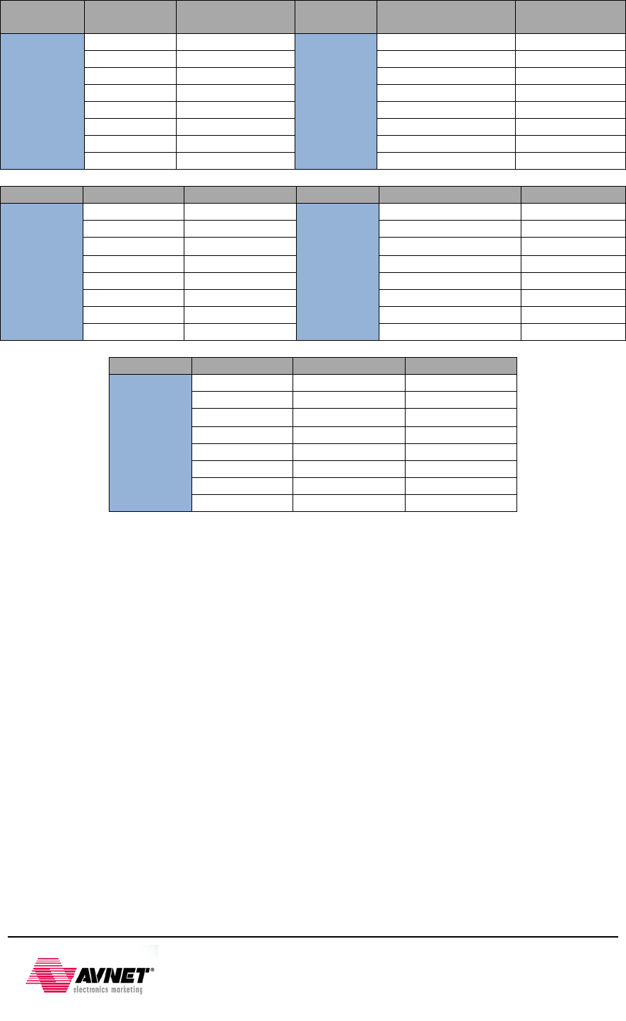
Table 16 - Pmod Connections
Pmod
Signal
Name
Zynq pin
Pmod
Signal Name Zynq pin
JA1
JA1
Y11
JB1
JB1
W12
JA2
AA11
JB2
W11
JA3
Y10
JB3
V10
JA4
AA9
JB4
W8
JA7
AB11
JB7
V12
JA8
AB10
JB8
W10
JA9
AB9
JB9
V9
JA10
AA8
JB10
V8
Pmod
Signal Name
Zynq pin
Pmod
Signal Name
Zynq pin
JC1
Differential
JC1_N
AB6
JD1
Differential
JD1_N
W7
JC1_P
AB7
JD1_P
V7
JC2_N
AA4
JD2_N
V4
JC2_P
Y4
JD2_P
V5
JC3_N
T6
JD3_N
W5
JC3_P
R6
JD3_P
W6
JC4_N
U4
JD4_N
U5
JC4_P
T4
JD4_P
U6
Pmod
Signal Name
Zynq pin
MIO
JE1
MIO Pmod
JE1
A6
MIO13
JE2
G7
MIO10
JE3
B4
MIO11
JE4
C5
MIO12
JE7
G6
MIO0
JE8
C4
MIO9
JE9
B6
MIO14
JE10
E6
MIO15
2.9.3 Agile Mixed Signaling (AMS) Connector, J2
The XADC header provides analog connectivity for analog reference designs, including AMS
daughter cards like Xilinx’s AMS Evaluation Card.
The analog header is placed close to the LPC FMC header as shown. Both analog and digital IO
can be easily supported for a plug in card. This allows the analog header to be easily connected
to the FMC card using a short ribbon cable as shown. The analog header can also be used
“stand alone” to support the connection of external analog signals.
The pin out has been chosen to provide tightly coupled differential analog pairs on the ribbon
cable and to also provide AGND isolation between channels. The plug in cards which will
facilitate a number of reference designs have not yet been designed so this pin out must provide
a reasonable degree of freedom while also keeping resource requirements as minimal as
possible.
27-Jan-2014
23
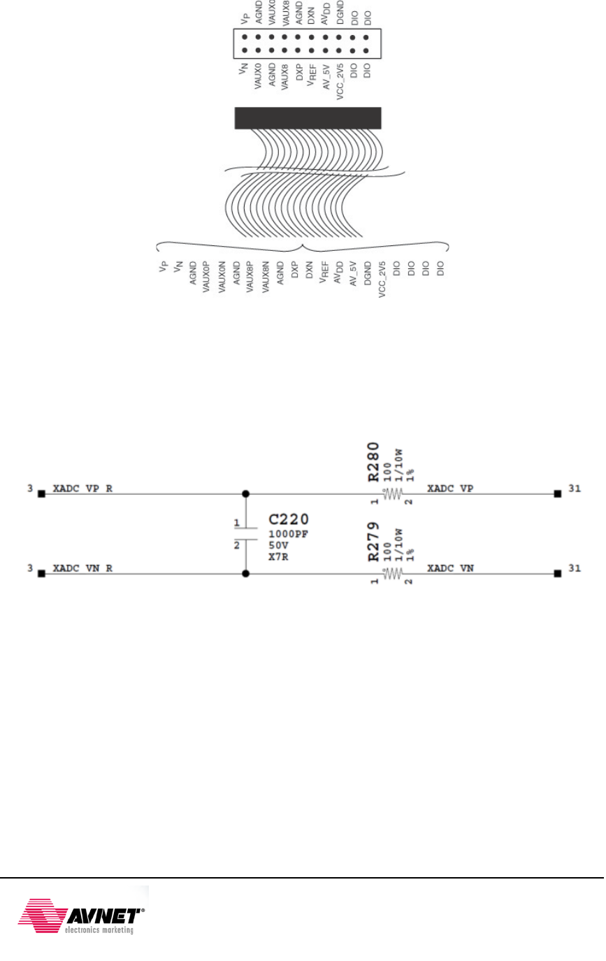
The ZedBoard AMS header is comparable with similar connectors on the Xilinx KC705 and
ZC702 boards. Any AMS plug-in cards built for those boards should be compatible with
ZedBoard as well.
Figure 13 - Analog Header Pin out
The following anti-aliasing filters were used for the XADC inputs:
- VP/VN
- VAUX0P/VAUX0N
- VAUX8P/VAUX8N
Figure 14 - Anti-Aliasing Filters for XADC Inputs
27-Jan-2014
24
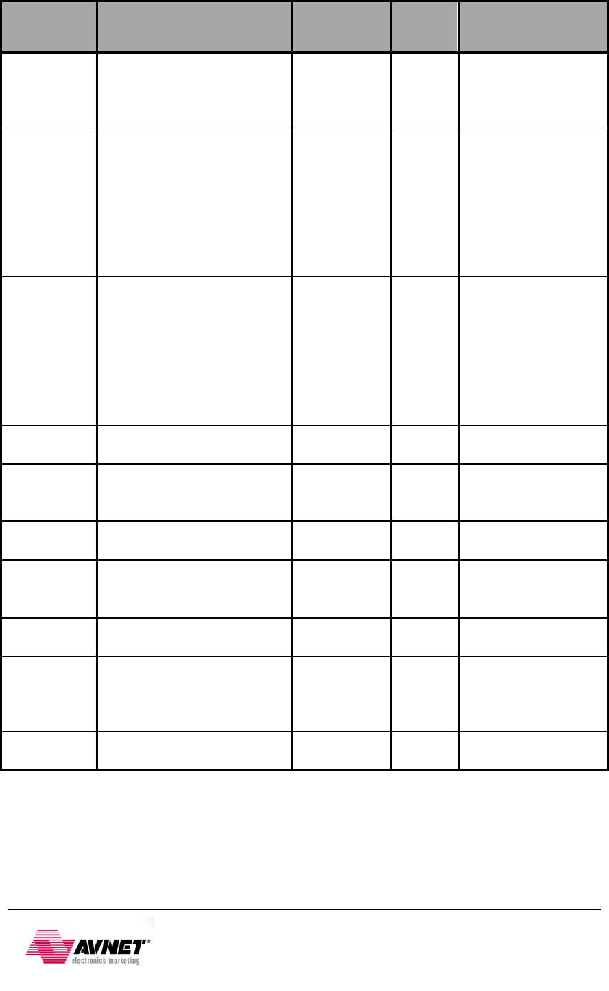
Table 17 - Analog Header Pin Out
Name Description Requirement XADC
Header Zynq Pin
VP/VN
Two pins required. Dedicated
pins on the 7 series package.
This is the dedicated analog
input channel for the ADC(s).
1V peak-to-
peak input
maximum
1
2
XADC-VN-R : M12
XADC-VP-R : L11
VAUX0P/VAUX0N
Two pins required. Auxiliary
analog input channel 0. Two
dedicated channels needed for
simultaneous sampling
applications. Should also
support use as IO inputs by
disconnection of anti-alias cap
see
1V peak-to-
peak input
maximum
6
3
XADC-AD0N-R : E16
XADC-AD0P-R : F16
VAUX8P/VAUX8N
Two pins required. Auxiliary
analog input channel 8. Two
dedicated channels needed for
simultaneous sampling
applications. Should also
support use as IO inputs by
disconnection of anti-alias cap
see
1V peak-to-
peak input
maximum
7
8
XADC-AD8N-R : D17
XADC-AD8P-R : D16
DXP/DXN
Two pins required. Access to
thermal Diode
12
9
XADC-DXN : N12
XADC-DXP : N11
AGND
Three pins required. Analog
ground reference GNDADC.
Analog channel isolation
4
5
10
VCCADC
One pin. This is the analog 1.8V
supply for XADC.
1.8V ±5%
@150mA max 14
VREF One pin. This is the 1.25V
reference from the board.
1.25V ±0.2%
50ppm/ºC
@5mA max
11
AV_5V Filtered 5V supply from board.
5V ±5%
@150mA max 13
GPIO General Purpose I/O
Voltage set by
Vadj
G0: 18
G1: 17
G2: 20
G3: 19
H15
R15
K15
J15
Vadj Adjustable Voltage, set by J18
1.8V, 2.5V,
3.3V
27-Jan-2014
25
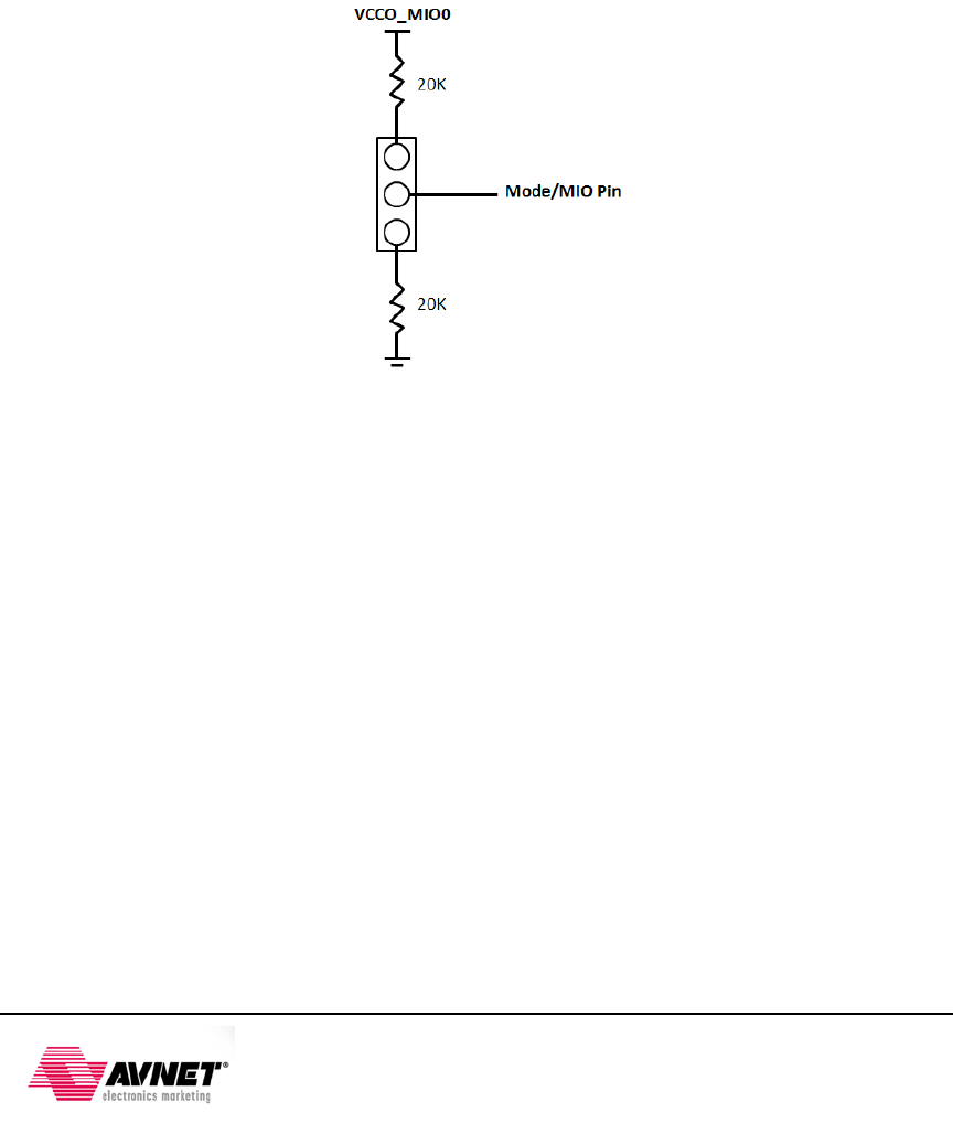
2.10 Configuration Modes
Zynq-7000 AP SoC devices use a multi-stage boot process that supports both non-secure and
secure boot (note that secure boot is not supported for CES silicon.) The PS is the master of the
boot and configuration process. The following table shows the Zynq configuration modes. Upon
reset, the device mode pins are read to determine the primary boot device to be used: NOR,
NAND, Quad-SPI, SD Card or JTAG.
By default, the ZedBoard uses the SD Card configuration mode. The boot mode pins are
MIO[8:2] and are used as follows:
• MIO[2]/Boot_Mode[3] sets the JTAG mode
• MIO[5:3]/Boot_Mode[2:0] select the boot mode
• MIO[6]/Boot_Mode[4] enables the internal PLL
• MIO[8:7]/Vmode[1:0] are used to configure the I/O bank voltages, however these are
fixed on ZedBoard and not configurable
The ZedBoard provides jumpers for MIO[6:2]. These are 1x3 jumpers connected as shown
below. All mode pins can be pulled high or low through a 20 KΩ resistor.
Figure 15 - Configuration Mode Jumpers
These jumpers allow users to change the mode options, including using cascaded JTAG
configuration as well as using the internal PLL.
As noted above, the VMODE pins are strapped permanently to set Bank 500 and 501 voltages to
3.3V and 1.8V. These are not jumper selectable.
27-Jan-2014
26
The PS boot mode selections are shown in the table below, default setting highlighted in yellow:
Table 18 – ZedBoard Configuration Modes
Xilinx TRM
MIO[6]
MIO[5]
MIO[4]
MIO[3]
MIO[2]
Boot_Mode[4]
Boot_Mode[0]
Boot_Mode[2]
Boot_Mode[1]
Boot_Mode[3]
JTAG Mode
Cascaded
JTAG
0
Independent
JTAG
1
Boot Devices
JTAG
0
0
0
Quad-SPI
1
0
0
SD Card
1
1
0
PLL Mode
PLL Used
0
PLL
Bypassed
1
Bank Voltages
MIO Bank 500
3.3V
MIO Bank 501
1.8V
Expected configuration time using a 50MB/s QSPI flash is 250ms.
PUDC_B is pulled high on ZedBoard but can be pulled low via JP5. This active-low input enables
internal pull-ups during configuration on all SelectIO pins
A push button labeled “PROG” is connected to the Zynq PROG pin, T11, and pulled up. Pushing
the button connects PROG to ground. Pushing this button will clear the PL configuration
memory, effectively resetting the entire PL subsection. The PS is responsible for reconfiguring
the PL. Zynq will not automatically reconfigure the PL as in standard FPGAs. The user software
application must reprogram the PL. An interrupt will indicate a change in the devcfg.INT_STS
register and the configuration pin status can be read from the devcfg.STATUS register. When
configuration is complete, a blue LED, LD12, labeled DONE, will light.
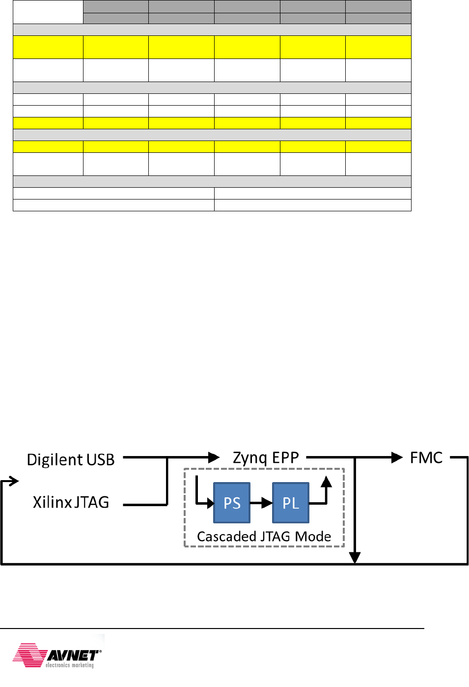
2.10.1 JTAG
As an alternative to using the onboard USB-JTAG interface, the ZedBoard provides traditional
Platform Cable JTAG connector, J15, for use with Xilinx Platform Cables and Digilent JTAG HS1
Programming Cables. The JTAG Chain is constructed as follows:
Figure 16 - ZedBoard JTAG Chain
27-Jan-2014
27
ZedBoard automatically adds the FMC into the JTAG chain when an FMC card is plugged into
the board via the FMC-PRSNT signal.
2.11 Power
2.11.1 Primary Power Input
The board’s primary input is through a 12V barrel jack. A compatible AC/DC converter will have a
2.5mm inner diameter, 5.5mm outer diameter, center positive connection.
The total power budget is based on 4A from an AC/DC wall wart supply. This rail is protected
with a TE 0603SFF600F/24-2.
A 10mΩ, 1W current sense resistor exists in series with the 12V input power supply. Header J21
straddles this resistor to measure the voltage across this resistor for calculating ZedBoard power.
Power is the measured voltage squared divided by the 10mΩ resistance.
2.11.2 On/Off Switch
ZedBoard includes an On/Off switch, SW8, to gate 12V. . When SW8 is in the OFF position, 12V
is disconnected from the board.
2.11.3 Regulators
The following Maxim power solution provides the power rails of the ZedBoard.
Figure 17 - Maxim Power Solution
27-Jan-2014
28
The table below shows the minimum required voltage rails, currents, and tolerances.
Table 19 - TPS65708 Connections
Voltage (V) Current (A) Tolerance
1.0 (Vccint) 1.3 5.00%
1.5 (Vccoddr) 1.5 5.00%
1.8 (Vccaux) 0.8 5.00%
1.8, 2.5, 3.3
(jumper adjustable, 2.5V
default) (Vadj)
2 5.00%
3.3 (Vcco/FMC/Pmod) 3 5.00%
1.8 (analog) (Vccadc) 0.15 5.00%
1.25 reference (Vrefp) 0.005 0.2%, 50ppm/ºC
0.75 (DDR3 Vtt) 1.5 5.00%
5.0 (Filtered for XADC) 0.15 5.00%
2.11.4 Sequencing
Sequencing for the power supplies follows the recommendations for the Zynq device. PS and PL
INT and AUX supplies are tied together on the ZedBoard platform to create a low cost design.
The following diagram illustrates the supply sequencing:
5V
1V Vccint
1.8V XADC
1.8V Vccaux
3.3V Vcco
Vadj (1.8/2.5/3.3)
1.5V Vccoddr
0.75V Vtt
1.25V Vref
Figure 18 - Power Sequencing
In addition to the sequencing, a power on reset circuit is used to hold the board in reset until all
power supplies have reached their regulation point.
27-Jan-2014
29
2.11.5 Power Good LED
A green status LED, LD13, indicates when power is good on the board. Power Good is wired
with the Resets and PROG to prevent operation of the board when power is not good.
2.11.6 Power Estimation
The Power estimation chart is shown below.
Table 20 – Current Usage Estimations, in mA
Feature
Part Number
MFG
Bank
1.0V
1.5V
1.8V
Vadj
3.3V
Zynq-7000 AP SoC PS Z7020-CLG484 Xilinx
600 250 150
150
Zynq-7000 AP SoC PL Z7020-CLG484 Xilinx
1200
300
50
DDR3
MT41K128M16HA-
15E:D
Micron VCCO_DDR
425
DDR3 Termination
360
QSPI Flash S25FL256S Vcc Spansion
100
QSPI Flash
S25FL256S Vio
Spansion
VCCO_MIO0
2
10/100/1000 PHY
88E1518 internal
Marvell
72
63
50
10/100/1000 PHY 88E1518 Vddo Marvell VCCO_MIO1
27
USB 2.0 OTG PHY TUSB1210 TI VCCO_MIO1
30
30
HDMI Transmitter
ADV7511
ADI
181
0
Audio Codec
ADAU1761
ADI
58
OLED UG-2832HSWEG04 Univision
28
Clock F4100 Fox
40
USB JTAG
SMT1
Digilent
110
UART to USB
CY7C64225
Cypress
VCCO_MIO1
26
SD Card
VCCO_MIO1
100
PS User LED (green)
VCCO_MIO0
5
PL User LEDs (green)
x8
40
PS User PB x2
VCCO_MIO0
0
PL User PBs x5
0
PL User Slide Switches
x8
0
Status LEDs (amber)
x4?
20
DONE LED (blue)
5
PS Pmod
TE 5-534206-6
TE
VCCO_MIO0
3000
PL Pmod #1 TE 5-534206-6 TE
PL Pmod #2 TE 5-534206-6 TE
PL Pmod #3
TE 5-534206-6
TE
PL Pmod #4
TE 5-534206-6
TE
FMC-LPC
2000
Total
1872 1035 751 2000 3814
1.0 1.5 1.8 2.5 3.3
27-Jan-2014
30

2.11.7 Testing
The power circuitry has been tested to verify compliance with the Zynq power requirements, such
as:
• Tolerance
o 1.0V Vccint 0.95 to 1.05V
o Vccaux +/- 5%
o Vcco +/-5%
• Ramp time
o 0.20 to 50ms
o In-rush current must be controlled so the power circuitry is not overloaded at
start-up
• Monotonicity
o No negative dips in Vccint or Vccaux power-up ramps
• Sequencing
o Verify sequencing responds as expected based on design
• Refer to Zynq Datasheet for the latest requirements
2.11.8 Probes
Two ground test point are available on the board, J3 and J4. This allows easy access to attach
ground leads of two scope probes to the board without having to locate GND pins on a header.
27-Jan-2014
31
3 Zynq-7000 AP SoC Banks
The following figure and table show Zynq CLG484 I/O bank assignments on the Zynq board.
Figure 19 - Zynq I/O Banks
27-Jan-2014
32
3.1 Zynq-7000 AP SoC Bank Voltages
Table 21 - Zynq Bank Voltage Assignments
PS-Side
Bank Voltage (default)
MIO Bank 0/500 3.3V
MIO Bank 1/501 1.8V
DDR 1.5V
PL-Side
Bank0 3.3V
Bank 13 3.3V
Bank 33 3.3V
Bank 34 Vadj (2.5V)
Bank 35 Vadj (2.5V)
Note: Banks 34 and 35 are powered from an adjustable voltage rail. Jumper, J18, selects this
voltage. Selectable voltages include 1.8V, 2.5V and 3.3V. The 3.3V jumper was intentionally
unpopulated on ZedBoard as these banks primarily connect to the FMC interface and many FMC
cards are only 1.8V and 2.5V compatible. Connecting 3.3V to these cards can damage them, so
leaving this jumper unpopulated reduces the risk of damaging FMC cards.
27-Jan-2014
33
4 Jumper Settings
Table 22 - Jumper Settings
Ref Designator Description Default Setting Function
JP1 Microphone Input Bias Open – No Electret
Microphone
Short to enable Bias
Voltage for Electret
Microphone. Right
Channel only.
JP2 Vbus 5V Enable Open – 5V
Disconnected
Short to enable 5V
output to USB OTG
Connector, J13, for
either Host or OTG
modes.
JP3 USB Vbus Capacitor
Setting Open – Device
Mode
Short for Host mode
(>120uF).
Open for Device or OTG
modes (4.7uF).
JP4 CFGBVS Select Not Populated
Pre-configuration I/O
standard type for the
dedicated configuration
bank 0. Vcco_0 is 3.3V,
Connected to 3.3V
through a 10K resistor.
This jumper connects to
GND and should NOT
be used.
JP5 PUDC Select Not Populated
Active Low input enables
internal pull-ups during
configuration on
all SelectIO pins.
Connected to Vadj
through 10K resistor.
JP6 PS_MIO0 Pull-Down Short
Install for SD Card boot
on CES silicon.
JP7
Boot_Mode[3]/MIO[2]
GND – Cascaded
JTAG
JTAG Mode. GND
cascades PS and PL
JTAG chains. VCC
makes JTAG chains
independent.
JP8
JP9
JP10
Boot_Mode[0]/MIO[3]
Boot_Mode[1]/MIO[4]
Boot_Mode[2]/MIO[5]
110 – SD Card
Boot Device Select
See Zynq Configuration
Modes
JP11 Boot_Mode[4]/MIO[6] GND – PLL Used
PLL Select. GND uses
PS PLLs. VCC
bypasses internal PS
PLLs
JP12 XADC Ferrite Bead
Disable Open
Short bypasses XADC-
GND ferrite bead
connection to board
GND.
JP13 JTAG PS-RST Open
Short connects JTAG
PROG-RST to PS
Reset.
J18 Vadj Select 1.8V
Selects Vadj (1.8V, 2.5V,
or 3.3V)
27-Jan-2014
34
Figure 20 - ZedBoard Jumper Map
27-Jan-2014
35
5 Mechanical
The ZedBoard measures 6.3”x6.3”.
Figure 21 - ZedBoard Mechanical
27-Jan-2014
36

6 Revision History
Rev date Rev # Reason for change
8/1/12
1.0
Initial ZedBoard User’s Guide
8/2/12
1.1
Mapped Configuration Mode Table to match ZedBoard layout
8/14/12 1.2
Added MIO Pins and Peripheral Tables; Updated Reset Section;
Updated Block Diagram
8/15/12
1.3
Updated Part Package numbering; Matched Xilinx Trademarks
8/30/12
1.4
Updated Board Images to Rev. C.1; Updated DDR3 section
9/4/12 1.5
Corrected package information in ZedBoard Block Diagram (fig. 1);
Added note regarding connecting multiple Pmods
9/5/12
1.6
Fixed error in Pmod Pinout Table
1/17/13
1.7
Added TI USB OTG PHY design advisory notice
1/18/13 1.8
Added LD9 to docs; Updated Default Jumper Table; Updated
Configuration Modes Table
1/29/13
1.9
Replaced RJ-45 184808-7 (obsolete) with 1840750-7
10/2/13 2.0
Removed ‘ES’ designation from Zynq part number. Corrected DDR3
IC25/IC26 placement description with IC26 being closest to the
Zynq. Removed references to the Xilinx Answer Record for DDR
training calculations as these are now included in the Xilinx tools.
11/1/13
2.1
Corrected reference to JE1’s MIO usage. Added MIO to Table 16.
1/27/14
2.2
Updated DDR3 trace impedance used vs. UG933 recommendation.
27-Jan-2014
37
