Gb Cpu Manual
User Manual: Pdf
Open the PDF directly: View PDF ![]() .
.
Page Count: 139 [warning: Documents this large are best viewed by clicking the View PDF Link!]
- Table of Contents
- 1. Foreword
- 2. Hardware specifications
- 2.1. Forward:
- 2.2. Terms
- 2.3. Game Boy Specs
- 2.4. Processor
- 2.5. Memory Map
- 2.6. Cartridge Types
- 2.7. Special modi
- 2.8. Video
- 2.9. Sound
- 2.10. Timer
- 2.11. Serial I/O
- 2.12. Interrupts
- 2.13. Special Registers
- 2.13.1. I/O Registers
- 1. FF00 (P1)
- 2. FF01 (SB)
- 3. FF02 (SC)
- 4. FF04 (DIV)
- 5. FF05 (TIMA)
- 6. FF06 (TMA)
- 7. FF07 (TAC)
- 8. FF0F (IF)
- 9. FF10 (NR 10)
- 10. FF11 (NR 11)
- 11. FF12 (NR12)
- 12. FF13 (NR 13)
- 13. FF14 (NR 14)
- 14. FF16 (NR 21)
- 15. FF17 (NR 22)
- 16. FF18 (NR 23)
- 17. FF19 (NR 24)
- 18. FF1A (NR 30)
- 19. FF1B (NR 31)
- 20. FF1C (NR 32)
- 21. FF1D (NR 33)
- 22. FF1E (NR 34)
- 23. FF20 (NR 41)
- 24. FF21 (NR 42)
- 25. FF22 (NR 43)
- 26. FF23 (NR 44)
- 27. FF24 (NR 50)
- 28. FF25 (NR 51)
- 29. FF26 (NR 52)
- 30. FF30 - FF3F (Wave Pattern RAM)
- 31. FF40 (LCDC)
- 32. FF41 (STAT)
- 33. FF42 (SCY)
- 34. FF43 (SCX)
- 35. FF44 (LY)
- 36. FF45 (LYC)
- 37. FF46 (DMA)
- 38. FF47 (BGP)
- 39. FF48 (OBP0)
- 40. FF49 (OBP1)
- 41. FF4A (WY)
- 42. FF4B (WX)
- 43. FFFF (IE)
- 2.13.1. I/O Registers
- 3. Game Boy command overview
- 4. Super Game Boy commands
- 4.1. Foreword
- 4.2. Palettes
- 4.3. SGB Border
- 4.4. Main Action Window
- 4.5. Commands
- 1. Set SGB color Palettes
- 2. "Block" Area Designation Mode ($04)
- 3. "Line" Area Designation Mode ($05)
- 4. "Divide" Area Designation Mode ($06)
- 5. "1CHR" Area Designation Mode ($07)
- 6. Sound On/Off ($08)
- 7. Transfer Sound PRG/DATA ($09)
- 8. Set System Color Palette Data ($0b)
- 9. Enable/Disable Attraction Mode ($0c)
- 10. Speed Function ($0d)
- 11. SGB Function ($0e)
- 12. Super NES WRAM Transfer 1 ($0f)
- 13. Super NES WRAM Transfer 2 ($10)
- 14. Controller 2 Request (#11) ($00) - Request 1 play
- 15. Controller 2 Request (#11) ($01) - Request 2 play
- 16. Set Program Counter ($12)
- 17. CharSet Transfer ($13)
- 18. Picture Transfer ($14) - Download border to SNES.
- 19. Set Attribute from ATF ($15)
- 20. Set Data from ATF ($16) (data)
- 21. GameBoy Window Mask ($17) (data)
- 22. Super NES OBJ Mode ($18)
- 23. SNES Color Palette Info
- 24. SGB Palette Selection
- 5. Appendix A
- Command Index
Sources by: Pan of Anthrox, GABY, Marat Fayzullin,
Pascal Felber, Paul Robson, Martin Korth, kOOPa, Bowser
Contents:
Assembly Language Commands, Timings and Opcodes, and
everything you always wanted to know about GB but were
afraid to ask.
THIS DOCUMENT IS PRINTED ON DIN A5 SIZE PAPER
(148mm x 210mm)!
Note: Game BoyTM, Game Boy PocketTM, Super Game BoyTM and Game
Boy ColorTM are registered trademarks of Nintendo CO., LTD.
© 1989 to 1999 by Nintendo CO., LTD.
Version: 1.01 by DP
Game BoyTM
CPU Manual

1. Foreword Game BoyTM CPU Manual
Table of Contents
1. Foreword...........................................4
2. Hardware speci f i cat i ons ............................5
2. 1. Forward: .......................................5
2. 2. Ter ms..........................................5
2. 3. Game Boy Specs.................................6
2. 4. Proces s or ......................................6
2. 5. Memor y Map.....................................8
2. 5. 1. Gener al memor y map.........................8
2. 5. 2. Echo of 8kB I nt er nal RAM...................9
2. 5. 3. User I / O...................................9
2. 5. 4. Res er ved Memor y Locat i ons .................10
2. 6. Cart ri dge Types ...............................13
2. 7. Speci al modi ..................................17
2. 7. 1. Power Up Sequence.........................17
2. 7. 2. St op Mode.................................19
2. 7. 3. Low- Power Mode............................19
2. 8. Vi deo.........................................22
2. 8. 1. Ti l es .....................................22
2. 8. 2. Spr i t es ...................................25
2. 8. 3. Spr i t e RAM Bug............................27
2. 9. Sound.........................................28
2. 10. Ti mer ........................................30
2. 11. Ser i al I / O...................................31
2. 12. I nt er rupt s ...................................32
2. 12. 1. I nt er r upt Pr ocedur e......................32
2. 12. 2. I nt er r upt Descr i pt i ons ...................34
2. 13. Speci al Regi s t er s............................35
2. 13. 1. I / O Regi s t er s............................35
Page 2 V 1.01

Game BoyTM CPU Manual 1. Foreword
3. Game Boy command overvi ew.........................61
3. 1. Foreword......................................61
3. 2. CPU Regi st ers .................................61
3. 2. 1. Gener al l y.................................61
3. 2. 2. Fl ag Regi st er .............................62
3. 2. 3. Pr ogr am Count er ...........................63
3. 2. 4. St ack Poi nt er .............................63
3. 3. Commands......................................65
3. 3. 1. 8- Bi t Loads...............................65
3. 3. 2. 16- Bi t Loads..............................76
3. 3. 3. 8- Bi t ALU.................................80
3. 3. 4. 16- Bi t Ar i t hmet i c.........................90
3. 3. 5. Mi scel l aneous .............................94
3. 3. 6. Rot at es & Shi f t s..........................99
3. 3. 7. Bi t Opcodes ..............................108
3. 3. 8. Jumps....................................111
3. 3. 9. Cal l s ....................................114
3. 3. 10. Res t ar t s................................116
3. 3. 11. Ret ur ns .................................117
4. Super Game Boy commands..........................119
4. 1. Foreword.....................................119
4. 2. Pal et t es.....................................119
4. 3. SGB Border...................................120
4. 4. Mai n Act i on Wi ndow...........................121
4. 5. Commands.....................................122
5. Appendi x A.......................................134
5. 1. Emul at or Not es ...............................134
5. 2. Typi cal t i mi ng di agram.......................137
by DP Page 3

1. Foreword Game BoyTM CPU Manual
1. Foreword
This Document was designed to help you programming the
Ga me B o y TM
Classic, Ga me B o y TM
Pocket, Super Game BoyTM
and Ga me B o y TM
Color (basics - you will need additional
document s f or GBC s peci f i c pr ogr ammi ng). It was ment to
be a compl et e handbook t o st ar t r i ght of f codi ng f or
the hardware. The documents consists of three major
par t s .
The first is the 'GBSpec.txt' (also known as the Pan
Do c u me n t ) b y Pan of An t h r ox , Ma r a t F a y z u l l i n , Pa s c a l
Fe l b e r , Pa u l Ro bs on , Ma r t i n K o r t h , kOOPa. This will be
found in paragraph 1.
The s e c on d i s a mi xt u r e of s e ve r a l do c ume nt s f r o m
'Game Boy Assembly Language Primer (GALP) V1.0'by GA BY
(GAmeBoY). It contains opcodes, time duration and the
affect ed fl ags per ASM command and t he. Thi s can be
found in paragraph 2.
The third is a summary of specifications and commands
for Nintendo Super Game Boy speciffic programming by
kOOPa and Bo ws e r . See paragraph 3.
Information on how to get your emulator proved
pr ogr ams r un on a r eal Game Boy can be f ound i n t he
Ap p e n d i x ( t h a n k s t o k OOP a ) . Also, a timing diagram of a
typical read and write operation on the classic GB bus
can be found here ( t hanks t o Phi l i ppe Poul i quen) .
On the last page a quick reference of ASM commands is
included.
Ha v e f u n !
DP
Page 4 V 1.01
Game BoyTM CPU Manual 2. Hardware specifications
2. Hardware specifications
2.1. Forward:
The f o l l o wi n g wa s t y p e d up f o r i n f o r ma t i o n a l p u r pos e s
regarding the inner workings on the hand-held game
ma c h i n e k n o w n a s G a me B o y , ma n u f a c t u r e d a n d d e s i g n e d b y
Ni n t e n d o Co . , L T D. T h i s i n f o i s p r e s e n t e d t o i n f o r m a
user on how t hei r Game Boy wor ks and what makes i t
"t i ck". GameBoy i s copyri ght ed by Ni nt endo Co. , LTD.
An y r e f e r e n c e t o c o p y r i g h t e d ma t e r i a l i s n o t p r e s e n t e d
for monetary gain, but for educational purposes and
hi gher l ear ni ng.
2.2. Terms
GB = Original GameBoy (GameBoy Classic)
GBP = GameBoy Pocket/GameBoy Light
GBC = GameBoy Color
SGB = Super GameBoy
by DP Page 5

2.3. Game Boy Specs Game BoyTM CPU Manual
2.3. Game Boy Specs
•CPU: 8 - b i t ( Si mi l a r t o t h e Z8 0 p r o c e s s o r . )
•Ma i n R A M: 8 K B y t e
•Vi d e o RAM: 8 K By t e
•Scr e e n Si ze 2. 6"
•Re s o l u t i o n : 1 6 0 x 1 4 4 ( 2 0 x 1 8 t i l e s )
•Ma x # o f s p r i t e s : 4 0
•Ma x # s p r i t e s / l i n e : 1 0
•Ma x s p r i t e s i z e : 8 x 1 6
•Mi n s p r i t e s i z e : 8 x 8
•Cl o c k S p e e d : 4 . 1 9 4 3 0 4 MHz
(4.295454 SGB, 4.194/8.388MHz GBC)
•Ho r i z S y n c : 9 1 9 8 KHz ( 9 4 2 0 KHz f o r S GB)
•Ve r t S y n c : 5 9 . 7 3 Hz ( 6 1 . 1 7 Hz f o r S GB)
•Sound: 4 channe l s wi t h s t er eo s ound
•Powe r : DC6V 0. 7W ( DC3V 0. 7W f or GB Poc ke t )
Nintendo documents describe the CPU & instructions
speed in machine cycl es whi le t hi s document describes
them in clock cycles. Here is the translation:
1 machine cycle = 4 clock cycles
GB CPU Speed NOP Instruction
Ma c h i n e C y c l e s 1.05MHz 1 cycle
Cl o c k Cy c l e s 4.19MHz 4 cycles
2.4. Processor
The GameBoy uses a computer chip similar to an Intel
8080. It contains all of the instructions of an 8080
except there are no exchange instructions. In many
ways the processor is more similar to the Zilog Z80
processor. Compared to the Z80, some instructions
Page 6 V 1.01

Game BoyTM CPU Manual 2.4. Processor
have been added and some have been taken away.
The following are added instructions:
ADD SP,nn ;nn = signed byte
LDI (HL),A ;Write A to (HL) and increment HL
LDD (HL),A ;Write A to (HL) and decrement HL
LDI A,(HL) ;Write (HL) to A and increment HL
LDD A,(HL) ;Write (HL) to A and decrement HL
LD A,($FF00+nn)
LD A,($FF00+C)
LD ($FF00+nn),A
LD ($FF00+C),A
LD (nnnn),SP
LD HL,SP+nn ;nn = signed byte
STOP ;Stop processor & screen until
button press
SWAP r ;Swap high & low nibbles of r
The following instructions have been removed:
Any command that uses the IX or IY registers.
All IN/OUT instructions.
All exchange instructions.
All commands prefixed by ED (except remapped RETI).
All conditional jumps/calls/rets on parity/overflow
and sign flag.
The following instructions have different opcodes:
LD A,[nnnn]
LD [nnnn],A
RETI
by DP Page 7

2.5. Memory Map Game BoyTM CPU Manual
2.5. Memory Map
2.5.1. General memory map
Interrupt Enable Register
--------------------------- FFFF
Internal RAM
--------------------------- FF80
Empty but unusable for I/O
--------------------------- FF4C
I/O ports
--------------------------- FF00
Empty but unusable for I/O
--------------------------- FEA0
Sprite Attrib Memory (OAM)
--------------------------- FE00
Echo of 8kB Internal RAM
--------------------------- E000
8kB Internal RAM
--------------------------- C000
8kB switchable RAM bank
--------------------------- A000
8kB Video RAM
--------------------------- 8000 --
16kB switchable ROM bank |
--------------------------- 4000 | = 32kB Cartrigbe
16kB ROM bank #0 |
--------------------------- 0000 --
* NOTE: b = bit, B = byte
Page 8 V 1.01

Game BoyTM CPU Manual 2.5.2. Echo of 8kB Internal RAM
2.5.2. Echo of 8kB Internal RAM
The addresses E000-FE00 appear to access the internal
RAM t h e s a me a s C0 0 0 - DE0 0 . ( i . e . I f y o u wr i t e a b y t e t o
address E000 i t wi l l appear at C000 and E000.
Si mi l ar l y, wr i t i ng a byt e t o C000 wi l l appea r at C000
and E000. )
2.5.3. User I/O
There are no empty spaces in the memory map for
implementing input ports except the switchable RAM bank
area (not an opt i on on t he Super Smar t Car d si nce i t ' s
RAM b a n k i s a l wa y s e n a b l e d ) . An o u t p u t o n l y p o r t ma y b e
implemented anywhere between A000-FDFF. If implemented
in a RAM area care should be taken to use an area of
RAM n o t u s e d f o r a n y t h i n g e l s e . ( F E0 0 a n d a b o v e c a n ' t
be us ed because t he CPU doesn' t gener at e an ext er nal
/WR for these locations.)
If you have a cart with an MBC1, a ROM 4Mbit or
smal l er, and a RAM 8Kbyt e or smal l er (or no RAM) t hen
you can use pi ns 6 & 7 of t he MBC1 f or 2 di gi t al out put
pi ns f or what ever pur pos e you wi s h. To us e t hem you
mu s t f i r s t p u t t h e MB C 1 i n t o 4 Mb i t R O M/ 3 2 K b y t e R A M mo d e
by wr i t i ng 01 t o 6000. The t wo l eas t si gni f i cant bi t s
you wr i t e t o 4000 wi l l t hen be out put t o t hese pi ns .
by DP Page 9

2.5.4. Reserved Memory Locations Game BoyTM CPU Manual
2.5.4. Reserved Memory Locations
0000 Restart $00 Address
(RST $00 calls this address.)
0008 Restart $08 Address
(RST $08 calls this address.)
0010 Restart $10 Address
(RST $10 calls this address.)
0018 Restart $18 Address
(RST $18 calls this address.)
0020 Restart $20 Address
(RST $20 calls this address.)
0028 Restart $28 Address
(RST $28 calls this address.)
0030 Restart $30 Address
(RST $30 calls this address.)
0038 Restart $38 Address
(RST $38 calls this address.)
0040 Vertical Blank Interrupt Start Address
0048 LCDC Status Interrupt Start Address
0050 Timer Overflow Interrupt Start Address
0058 Serial Transfer Completion Interrupt
Start Address
0060 High-to-Low of P10-P13 Interrupt
Start Address
An i n t e r n a l i n f o r ma t i o n a r e a i s l o c a t e d a t 0 1 0 0 - 0 1 4 F i n
each cart ri dge. I t cont ai ns t he f ol l owi ng val ues:
0100- 0103 This is the begin code execution point in a
cart. Usually there is a NOP and a JP
instruction here but not always.
Page 10 V 1.01

Game BoyTM CPU Manual 2.5.4. Reserved Memory
Locations
0104- 0133 Scrolling Nintendo graphic:
CE ED 66 66 CC 0D 00 0B 03 73 00 83 00 0C 00 0D
00 08 11 1F 88 89 00 0E DC CC 6E E6 DD DD D9 99
BB BB 67 63 6E 0E EC CC DD DC 99 9F BB B9 33 3E
( PROGRAM WON'T RUN IF CHANGED!!!)
0134- 0142 Title of the game in UPPER CASE ASCII. If it
is less than 16 characters then the
remaining bytes are filled with 00's.
0143 $80 = Color GB, $00 or other = not Color GB
0144 Ascii hex digit, high nibble of licensee
code (new).
0145 Ascii hex digit, low nibble of licensee
code (new). (These are normally $00 if
[$014B] <> $33.)
0146 GB/SGB Indicator (00 = GameBoy, 03 = Super
GameBoy functions)
(Super GameBoy functions won't work
if <> $03.)
0147 Cartridge type:
0-ROM ONLY 12-ROM+MBC3+RAM
1-ROM+MBC1 13-ROM+MBC3+RAM+BATT
2-ROM+MBC1+RAM 19-ROM+MBC5
3-ROM+MBC1+RAM+BATT 1A-ROM+MBC5+RAM
5-ROM+MBC2 1B-ROM+MBC5+RAM+BATT
6-ROM+MBC2+BATTERY 1C-ROM+MBC5+RUMBLE
8-ROM+RAM 1D-ROM+MBC5+RUMBLE+SRAM
9-ROM+RAM+BATTERY 1E-ROM+MBC5+RUMBLE+SRAM+BATT
B-ROM+MMM01 1F-Pocket Camera
C-ROM+MMM01+SRAM FD-Bandai TAMA5
D-ROM+MMM01+SRAM+BATT FE - Hudson HuC-3
by DP Page 11

2.5.4. Reserved Memory Locations Game BoyTM CPU Manual
F-ROM+MBC3+TIMER+BATT FF - Hudson HuC-1
10-ROM+MBC3+TIMER+RAM+BATT
11-ROM+MBC3
0148 ROM size:
0 - 256Kbit = 32KByte = 2 banks
1 - 512Kbit = 64KByte = 4 banks
2 - 1Mbit = 128KByte = 8 banks
3 - 2Mbit = 256KByte = 16 banks
4 - 4Mbit = 512KByte = 32 banks
5 - 8Mbit = 1MByte = 64 banks
6 - 16Mbit = 2MByte = 128 banks
$52 - 9Mbit = 1.1MByte = 72 banks
$53 - 10Mbit = 1.2MByte = 80 banks
$54 - 12Mbit = 1.5MByte = 96 banks
0149 RAM size:
0 - None
1 - 16kBit = 2kB = 1 bank
2 - 64kBit = 8kB = 1 bank
3 - 256kBit = 32kB = 4 banks
4 - 1MBit =128kB =16 banks
014A Destination code:
0 - Japanese
1 - Non-Japanese
014B Licensee code (old):
33 - Check 0144/0145 for Licensee code.
79 - Accolade
A4 - Konami
(Super GameBoy function won't work
if <> $33.)
014C Mask ROM Version number (Usually $00)
Page 12 V 1.01

Game BoyTM CPU Manual 2.5.4. Reserved Memory
Locations
014D Complement check
(PROGRAM WON'T RUN ON GB IF NOT CORRECT!!!)
(It will run on Super GB, however,
if incorrect.)
014E- 014F Checksum (higher byte first) produced by
adding all bytes of a cartridge except for
two checksum bytes and taking two lower
bytes of the result. (GameBoy ignores this
value.)
2.6. Cartridge Types
The f o l l o wi n g de f i n e t he b y t e a t c a r t l o c a t i o n 0147 :
•ROM ONLY
This is a 32kB (256kb) ROM and occupies 0000-7FFF.
•MB C 1 (Memory Bank Controller 1)
MBC1 has two different maximum memory modes:
16Mbit ROM/8KByte RAM or 4Mbit ROM/32KByte RAM.
The MBC1 defaults to 16Mbit ROM/8KByte RAM mode
on power up. Writing a value (XXXXXXXS - X = Don't
care, S = Memory model select) into 6000-7FFF area
will select the memory model to use. S = 0 selects
16/8 mode. S = 1 selects 4/32 mode.
Writing a value (XXXBBBBB - X = Don't cares, B =
bank select bits) into 2000-3FFF area will select
an appropriate ROM bank at 4000-7FFF. Values of 0
and 1 do the same thing and point to ROM bank 1.
by DP Page 13

2.6. Cartridge Types Game BoyTM CPU Manual
Rom bank 0 is not accessible from 4000-7FFF and can
only be read from 0000-3FFF.
If memory model is set to 4/32:
Writing a value (XXXXXXBB - X = Don't care, B =
bank select bits) into 4000-5FFF area will select
an appropriate RAM bank at A000-C000. Before you
can read or write to a RAM bank you have to enable
it by writing a XXXX1010 into 0000-1FFF area*. To
disable RAM bank operations write any value but
XXXX1010 into 0000-1FFF area. Disabling a RAM bank
probably protects that bank from false writes
during power down of the GameBoy. (NOTE: Nintendo
suggests values $0A to enable and $00 to disable
RAM bank!!)
If memory model is set to 16/8 mode:
Writing a value (XXXXXXBB - X = Don't care, B =
bank select bits) into 4000-5FFF area will set the
two most significant ROM address lines.
* NOTE: The Super Smart Card doesn't require this
operation because it's RAM bank is ALWAYS enabled.
Include this operation anyway to allow your code
to work with both.
•MB C 2 (Memory Bank Controller 2):
This memory controller works much like the MBC1
controller with the following exceptions:
MBC2 will work with ROM sizes up to 2Mbit.
Writing a value (XXXXBBBB - X = Don't cares, B =
bank select bits) into 2000-3FFF area will select
an appropriate ROM bank at 4000-7FFF.
RAM switching is not provided. Unlike the MBC1
which uses external RAM, MBC2 has 512 x 4 bits of
Page 14 V 1.01

Game BoyTM CPU Manual 2.6. Cartridge Types
RAM which is in the controller itself. It still
requires an external battery to save data during
power-off though.
The least significant bit of the upper address
byte must be zero to enable/disable cart RAM. For
example the following addresses can be used to
enable/disable cart RAM:
0000-00FF, 0200-02FF, 0400-04FF, ..., 1E00-1EFF.
enable/disable is 0000-00FF. The suggested address
range to use for MBC2 ram
The least significant bit of the upper address
byte must be one to select a ROM bank. For example
the following addresses can be used to select a ROM
bank: 2100-21FF, 2300-23FF, 2500-25FF, ..., 3F00-
3FFF. The suggested address range to use for MBC2
rom bank selection is 2100-21FF.
•MB C 3 (Memory Bank Controller 3):
This controller is similar to MBC1 except it
accesses all 16mbits of ROM without requiring any
writes to the 4000-5FFF area.
Writing a value (XBBBBBBB - X = Don't care, B =
bank select bits) into 2000-3FFF area will select
an appropriate ROM bank at 4000-7FFF.
Also, this MBC has a built-in battery-backed Real
Time Clock (RTC) not found in any other MBC. Some
MBC3 carts do not support it (WarioLand II non
color version) but some do (Harvest Moon/Japanese
version.)
•MB C 5 (Memory Bank Controller 5):
This controller is the first MBC that is guaranteed
to run in GameBoy Color double-speed mode but it
appears the other MBC's run fine in GBC double
speed mode as well.
by DP Page 15

2.6. Cartridge Types Game BoyTM CPU Manual
It is similar to the MBC3 (but no RTC) but can
access up to 64mbits of ROM and up to 1mbit of RAM.
The lower 8 bits of the 9-bit rom bank select is
written to the 2000-2FFF area while the upper bit
is written to the least significant bit of the
3000-3FFF area.
Writing a value (XXXXBBBB - X = Don't care, B =
bank select bits) into 4000-5FFF area will select
an appropriate RAM bank at A000-BFFF if the cart
contains RAM. Ram sizes are 64kbit,256kbit, &
1mbit.
Also, this is the first MBC that allows rom bank 0
to appear in the 4000-7FFF range by writing $000
to the rom bank select.
•Ru mb l e Ca r t s :
Rumble carts use an MBC5 memory bank controller.
Rumble carts can only have up to 256kbits of RAM.
The highest RAM address line that allows 1mbit of
RAM on MBC5 non-rumble carts is used as the motor
on/off for the rumble cart.
Writing a value (XXXXMBBB - X = Don't care, M =
motor, B = bank select bits) into 4000-5FFF area
will select an appropriate RAM bank at A000-BFFF
if the cart contains RAM. RAM sizes are 64kbit or
256kbits. To turn the rumble motor on set M = 1,
M = 0 turns it off.
•Hu C1 (Memory Bank / Infrared Controller):
This controller made by Hudson Soft appears to be
very similar to an MBC1 with the main difference
being that it supports infrared LED input / output.
The Japanese cart "Fighting Phoenix" (internal cart
name: SUPER B DAMAN) is known to contain this chip.
Page 16 V 1.01

Game BoyTM CPU Manual 2.7. Special modi
2.7. Special modi
2.7.1. Power Up Sequence
When the GameBoy is powered up, a 256 byte program
starting at memory location 0 is executed. This
program is located in a ROM inside the GameBoy. The
first thing the program does is read the cartridge
locations from $104 to $133 and place this graphic of
a Nintendo logo on the screen at the top. This image
is then scrolled until it is in the middle of the
screen. Two musical notes are then played on the
internal speaker. Again, the cartridge locations $104
to $133 are read but this time they are compared with
a table in the internal rom.
If any byte fails to compare, then the GameBoy stops
comparing bytes and simply halts all operations.
GB & GB P o c k e t :
Next, the GameBoy starts adding all of the bytes
in the cartridge from $134 to $14d. A value of 25
decimal is added to this total. If the least
significant byte of the result is a not a zero,
then the GameBoy will stop doing anything.
Super GB:
Even though the GB & GBP check the memory
locations from $134 to $14d, the SGB doesn't.
If the above checks pass then the internal ROM is
disabled and cartridge program execution begins at
location $100 with the following register values:
AF=$01-GB/SGB, $FF-GBP, $11-GBC
F =$B0
by DP Page 17

2.7.1. Power Up Sequence Game BoyTM CPU Manual
BC=$0013
DE=$00D8
HL=$014D
Stack Pointer=$FFFE
[$FF05] = $00 ; TIMA
[$FF06] = $00 ; TMA
[$FF07] = $00 ; TAC
[$FF10] = $80 ; NR10
[$FF11] = $BF ; NR11
[$FF12] = $F3 ; NR12
[$FF14] = $BF ; NR14
[$FF16] = $3F ; NR21
[$FF17] = $00 ; NR22
[$FF19] = $BF ; NR24
[$FF1A] = $7F ; NR30
[$FF1B] = $FF ; NR31
[$FF1C] = $9F ; NR32
[$FF1E] = $BF ; NR33
[$FF20] = $FF ; NR41
[$FF21] = $00 ; NR42
[$FF22] = $00 ; NR43
[$FF23] = $BF ; NR30
[$FF24] = $77 ; NR50
[$FF25] = $F3 ; NR51
[$FF26] = $F1-GB, $F0-SGB ; NR52
[$FF40] = $91 ; LCDC
[$FF42] = $00 ; SCY
[$FF43] = $00 ; SCX
[$FF45] = $00 ; LYC
[$FF47] = $FC ; BGP
[$FF48] = $FF ; OBP0
[$FF49] = $FF ; OBP1
[$FF4A] = $00 ; WY
[$FF4B] = $00 ; WX
[$FFFF] = $00 ; IE
Page 18 V 1.01

Game BoyTM CPU Manual 2.7.1. Power Up Sequence
It is not a good idea to assume the above values
will always exist. A later version GameBoy could
contain different values than these at reset.
Always set these registers on reset rather than
assume they are as above.
Please note that GameBoy internal RAM on power up
contains random data. All of the GameBoy emulators
tend to set all RAM to value $00 on entry.
Cart RAM the first time it is accessed on a real
GameBoy contains random data. It will only contain
known data if the GameBoy code initializes it to
some value.
2.7.2. Stop Mode
The STOP command halts the GameBoy processor
and screen until any button is pressed. The GB
and GBP screen goes white with a single dark
horizontal line. The GBC screen goes black.
2.7.3. Low-Power Mode
It is recommended that the HALT instruction be used
whenever possible to reduce power consumption & extend
the life of the batteries. This command stops the
system clock reducing the power consumption of both
the CPU and ROM.
The CPU will remain suspended until an interrupt
occurs at which point the interrupt is serviced and
then the instruction immediately following the HALT
by DP Page 19

2.7.3. Low-Power Mode Game BoyTM CPU Manual
is executed. If interrupts are disabled (DI) then
halt doesn't suspend operation but it does cause
the program counter to stop counting for one
instruction on the GB,GBP, and SGB as mentioned below.
Depending on how much CPU time is required by a game,
the HALT instruction can extend battery life anywhere
from 5 to 50% or possibly more.
WA R N I N G : The instruction immediately following the
HALT instruction is "skipped" when interrupts are
disabled (DI) on the GB,GBP, and SGB. As a result,
always put a NOP after the HALT instruction. This
instruction skipping doesn't occur when interrupts
are enabled (EI).
This "skipping" does not seem to occur on the
GameBoy Color even in regular GB mode. ($143=$00)
EXAMPLES from Martin Korth who documented this
problem:
(assuming interrupts disabled for all examples)
1) This code causes the 'a' register to be
incremented TWICE.
76 halt
3C inc a
2) The next example is a bit more difficult.
The following code
76 halt
FA 34 12 ld a,(1234)
is effectively executed as
76 halt
Page 20 V 1.01

Game BoyTM CPU Manual 2.7.3. Low-Power Mode
FA FA 34 ld a,(34FA)
12 ld (de),a
3) Finally an interesting side effect
76 halt
76 halt
This combination hangs the cpu.
The first HALT causes the second HALT to be
repeated, which therefore causes the following
command (=itself) to be repeated - again and again.
Placing a NOP between the two halts would cause the
NOP to be repeated once, the second HALT wouldn't
lock the cpu.
Below is suggested code for Game Boy programs:
; **** Main Game Loop ****
Main:
halt ; stop system clock
; return from halt when
; interrupted
nop ; (See WARNING above.)
ld a,(VblnkFlag)
or a ; V-Blank interrupt ?
jr z,Main ; No, some other
; interrupt
xor a
ld (VblnkFlag),a ; Clear V-Blank flag
call Controls ; button inputs
call Game ; game operation
jr Main
by DP Page 21

2.7.3. Low-Power Mode Game BoyTM CPU Manual
; **** V-Blank Interrupt Routine ****
Vblnk:
push af
push bc
push de
push hl
call SpriteDma ; Do sprite updates
ld a,1
ld (VblnkFlag),a
pop hl
pop de
pop bc
pop af
reti
2.8. Video
2.8.1. Tiles
The main GameBoy screen buffer (background) consists
of 256x256 pixels or 32x32 tiles (8x8 pixels each).
Only 160x144 pixels can be displayed on the screen.
Registers SCROLLX and SCROLLY hold the coordinates of
background to be displayed in the left upper corner of
the screen. Background wraps around the screen (i.e.
when part of it goes off the screen, it appears on the
opposite side.)
An area of VRAM known as Background Tile Map contains
the numbers of tiles to be displayed. It is organized
as 32 rows of 32 bytes each. Each byte contains a
Page 22 V 1.01

Game BoyTM CPU Manual 2.8.1. Tiles
number of a tile to be displayed. Tile patterns are
taken from the Tile Data Table located either at
$8000-8FFF or $8800-97FF. In the first case, patterns
are numbered with unsigned numbers from 0 to 255 (i.e.
pattern #0 lies at address $8000). In the second case,
patterns have signed numbers from -128 to 127 (i.e.
pattern #0 lies at address $9000). The Tile Data Table
address for the background can be selected via LCDC
register.
Besides background, there is also a "window"
overlaying the background. The window is not
scrollable i.e. it is always displayed starting from
its left upper corner. The location of a window on the
screen can be adjusted via WNDPOSX and WNDPOSY
registers. Screen coordinates of the top left corner
of a window are WNDPOSX-7,WNDPOSY. The tile numbers
for the window are stored in the Tile Data Table. None
of the windows tiles are ever transparent. Both the
Background and the window share the same Tile Data
Table.
Both background and window can be disabled or enabled
separately via bits in the LCDC register.
If the window is used and a scan line interrupt
disables it (either by writing to LCDC or by setting
WX > 166) and a scan line interrupt a little later on
enables it then the window will resume appearing on
the screen at the exact position of the window where
it left off earlier. This way, even if there are only
16 lines of useful graphics in the window, you could
display the first 8 lines at the top of the screen and
the next 8 lines at the bottom if you wanted to do so.
by DP Page 23

2.8.1. Tiles Game BoyTM CPU Manual
WX may be changed during a scan line interrupt (to
either cause a graphic distortion effect or to disable
the window (WX>166) ) but changes to WY are not
dynamic and won't be noticed until the next screen
redraw.
The tile images are stored in the Tile Pattern
Tables. Each 8x8 image occupies 16 bytes, where each 2
bytes represent a line:
Tile: Image:
.33333.. .33333. . - > 01111100 - > $7C
22...22. 01111100 - > $7C
11...11. 22...22. -> 00000000 -> $00
2222222. <-- digits 11000110 -> $C6
33...33. represent 11...11. -> 11000110 - > $C6
22...22. color 00000000 - > $00
11...11. numbers 2222222. -> 00000000 -> $00
........ 11111110 -> $FE
33...33. -> 11000110 -> $C6
11000110 -> $C6
22...22. - > 00000000 - > $00
11000110 - > $C6
11...11. -> 11000110 - > $C6
00000000 -> $00
........ -> 00000000 -> $00
00000000 -> $00
As it was said before, there are two Tile Pattern
Tables at $8000-8FFF and at $8800-97FF. The first one
can be used for sprites, the background, and the
window display. Its tiles are numbered from 0 to 255.
The second table can be used for the background and
the window display and its tiles are numbered from
-128 to 127.
Page 24 V 1.01

Game BoyTM CPU Manual 2.8.2. Sprites
2.8.2. Sprites
GameBoy video controller can display up to 40 sprites
either in 8x8 or in 8x16 pixels. Because of a
limitation of hardware, only ten sprites can be
displayed per scan line. Sprite patterns have the same
format as tiles, but they are taken from the Sprite
Pattern Table located at $8000-8FFF and have unsigned
numbering. Sprite attributes reside in the Sprite
Attribute Table (OAM - Object Attribute Memory) at
$FE00-FE9F. OAM is divided into 40 4-byte blocks each
of which corresponds to a sprite.
In 8x16 sprite mode, the least significant bit of the
sprite pattern number is ignored and treated as 0.
When sprites with different x coordinate values
overlap, the one with the smaller x coordinate (closer
to the left) will have priority and appear above any
others.
When sprites with the same x coordinate values
overlap, they have priority according to table
ordering. (i.e. $FE00 - highest, $FE04 - next highest,
etc.)
Please note that Sprite X=0, Y=0 hides a sprite. To
display a sprite use the following formulas:
SpriteScreenPositionX (Upper left corner of sprite)
= SpriteX - 8
SpriteScreenPositionY (Upper left corner of sprite)
= SpriteY - 16
by DP Page 25

2.8.2. Sprites Game BoyTM CPU Manual
To display a sprite in the upper left corner of the
screen set sprite X=8, Y=16.
Only 10 sprites can be displayed on any one line.
When this limit is exceeded, the lower priority
sprites (priorities listed above) won't be displayed.
To keep unused sprites from affecting onscreen sprites
set their Y coordinate to Y=0 or Y=>144+16. Just
setting the X coordinate to X=0 or X=>160+8 on a
sprite will hide it but it will still affect other
sprites sharing the same lines.
Blocks have the following
format:
Byte0 Y position on the screen
Byte1 X position on the screen
Byte2 Pattern number 0-255 (Unlike some tile
numbers, sprite pattern numbers are unsigned.
LSB is ignored (treated as 0) in 8x16 mode.)
Byte3 Flags:
Bit7 Priority
If this bit is set to 0, sprite is
displayed on top of background & window.
If this bit is set to 1, then sprite
will be hidden behind colors 1, 2, and 3
of the background & window. (Sprite only
prevails over color 0 of BG & win.)
Bit6 Y flip
Sprite pattern is flipped vertically if
this bit is set to 1.
Bit5 X flip
Sprite pattern is flipped horizontally
if this bit is set to 1.
Page 26 V 1.01

Game BoyTM CPU Manual 2.8.2. Sprites
Bit4 Palette number
Sprite colors are taken from OBJ1PAL if
this bit is set to 1 and from OBJ0PAL
otherwise.
2.8.3. Sprite RAM Bug
There is a flaw in the GameBoy hardware that causes
trash to be written to OAM RAM if the following
commands are used while their 16-bit content is in the
range of $FE00 to $FEFF:
inc xx (xx = bc,de, or hl)
dec xx
ldi a,(hl)
ldd a,(hl)
ldi (hl),a
ldd (hl),a
Only sprites 1 & 2 ($FE00 & $FE04) are not affected
by these instructions.
by DP Page 27

2.9. Sound Game BoyTM CPU Manual
2.9. Sound
There are two sound channels connected to the output
terminals SO1 and SO2. There is also a input terminal
Vin connected to the cartridge. It can be routed to
either of both output terminals. GameBoy circuitry
allows producing sound in four different ways:
Quadrangular wave patterns with sweep and envelope
functions. Quadrangular wave patterns with envelope
functions. Voluntary wave patterns from wave RAM.
White noise with an envelope function.
These four sounds can be controlled independantly and
then mixed separately for each of the output
terminals.
Sound registers may be set at all times while
pr oduci ng s ound.
When setting the initial value of the envelope and
restarting the length counter, set the initial flag to
1 and initialize the data.
Under the following situations the Sound ON flag is
reset and the sound output stops:
1. When the sound output is stopped by the length
counter.
2. When overflow occurs at the addition mode while
sweep is operating at sound 1.
When the Sound OFF flag for sound 3 (bit 7 of NR30)
is set at 0, the cancellation of the OFF mode must be
done by setting the sound OFF flag to 1. By
initializing sound 3, it starts it's function.
Page 28 V 1.01

Game BoyTM CPU Manual 2.9. Sound
When the All Sound OFF flag (bit 7 of NR52) is set to
0, the mode registers for sounds 1,2,3, and 4 are
reset and the sound output stops. (NOTE: The setting
of each sounds mode register must be done after the
All Sound OFF mode is cancelled. During the All Sound
OFF mode, each sound mode register cannot be set.)
NOTE: DURING THE ALL SOUND OFF MODE, GB POWER
CONSUMPTION DROPS BY 16% OR MORE! WHILE YOUR PROGRAMS
AREN'T USING SOUND THEN SET THE ALL SOUND OFF FLAG TO
0. IT DEFAULTS TO 1 ON RESET.
These tend to be the two most important equations in
converting between Hertz and GB frequency registers:
(Sounds will have a 2.4% higher frequency on Super
GB.)
gb = 2048 - (131072 / Hz)
Hz = 131072 / (2048 - gb)
by DP Page 29

2.10. Timer Game BoyTM CPU Manual
2.10. Timer
Sometimes it's useful to have a timer that interrupts
at regular intervals for routines that require
periodic or percise updates. The timer in the GameBoy
has a selectable frequency of 4096, 16384, 65536, or
262144 Hertz. This frequency increments the Timer
Counter (TIMA). When it overflows, it generates an
interrupt. It is then loaded with the contents of
Timer Modulo (TMA). The following are examples:
;This interval timer interrupts 4096 times per second
ld a,-1
ld ($FF06),a ;Set TMA to divide clock by 1
ld a,4
ld ($FF07),a ;Set clock to 4096 Hertz
;This interval timer interrupts 65536 times per second
ld a,-4
ld ($FF06),a ;Set TMA to divide clock by 4
ld a,5
ld ($FF07),a ;Set clock to 262144 Hertz
Page 30 V 1.01

Game BoyTM CPU Manual 2.11. Serial I/O
2.11. Serial I/O
The serial I/O port on the Gameboy is a very simple
setup and is crude compared to standard RS-232 (IBM-
PC) or RS-485 (Macintosh) serial ports. There are no
start or stop bits so the programmer must be more
creative when using this port.
During a transfer, a byte is shifted in at the same
time that a byte is shifted out. The rate of the shift
is deter- mined by whether the clock source is
internal or external. If internal, the bits are
shifted out at a rate of 8192Hz (122 microseconds) per
bit. The most significant bit is shifted in and out
first.
When the internal clock is selected, it drives the
clock pin on the game link port and it stays high when
not used. During a transfer it will go low eight times
to clock in/out each bit.
A programmer initates a serial transfer by setting bit
7 of $FF02. This bit may be read and is automatically
set to 0 at the completion of transfer. After this bit
is set, an interrupt will then occur eight bit clocks
later if the serial interrupt is enabled.
If internal clock is selected and serial interrupt is
enabled, this interrupt occurs 122*8 microseconds
later.
If external clock is selected and serial interrupt is
enabled, an interrupt will occur eight bit clocks
later.
Initiating a serial transfer with external clock will
wait forever if no external clock is present. This
by DP Page 31

2.11. Serial I/O Game BoyTM CPU Manual
allows a certain amount of synchronization with each
serial port.
The state of the last bit shifted out determines the
state of the output line until another transfer takes
place.
If a serial transfer with internal clock is performed
and no external GameBoy is present, a value of $FF
will be received in the transfer.
The following code causes $75 to be shifted out the
serial port and a byte to be shifted into $FF01:
ld a,$75
ld ($FF01),a
ld a,$81
ld ($FF02),a
2.12. Interrupts
2.12.1. Interrupt Procedure
The IME (interrupt master enable) flag is reset by DI
and prohibits all interrupts. It is set by EI and
acknowledges the interrupt setting by the IE register.
1. When an interrupt is generated, the IF flag will be
set.
2. If the IME flag is set & the corresponding IE flag
is set, the following 3 steps are performed.
3. Reset the IME flag and prevent all interrupts.
4. The PC (program counter) is pushed onto the stack.
5. Jump to the starting address of the interrupt.
Page 32 V 1.01

Game BoyTM CPU Manual 2.12.1. Interrupt Procedure
Resetting of the IF register, which was the cause of
the interrupt, is done by hardware.
During the interrupt, pushing of registers to be used
should be performed by the interrupt routine.
Once the interrupt service is in progress, all the
interrupts will be prohibited. However, if the IME
flag and the IE flag are controlled, a number of
interrupt services can be made possible by nesting.
Return from an interrupt routine can be performed by
either RETI or RET instruction.
The RETI instruction enables interrupts after doing a
return operation.
If a RET is used as the final instruction in an
interrupt routine, interrupts will remain disabled
unless a EI was used in the interrupt routine or is
used at a later time. The interrupt will be
acknowledged during opcode fetch period of each
instruction.
by DP Page 33

2.12.2. Interrupt Descriptions Game BoyTM CPU Manual
2.12.2. Interrupt Descriptions
The following interrupts only occur if they have been
enabled in the Interrupt Enable register ($FFFF) and
if the interrupts have actually been enabled using the
EI instruction.
1. V-Blank
The V-Blank interrupt occurs ~59.7 times a second
on a regular GB and ~61.1 times a second on a Super
GB (SGB). This interrupt occurs at the beginning of
the V-Blank period. During this period video
hardware is not using video ram so it may be freely
accessed. This period lasts approximately 1.1 ms.
2. LCDC Status
There are various reasons for this interrupt to
occur as described by the STAT register ($FF40). One
very popular reason is to indicate to the user when
the video hardware is about to redraw a given LCD
line. This can be useful for dynamically controlling
the SCX/SCY registers ($FF43/$FF42) to perform
special video effects.
3. Timer Overflow
This interrupt occurs when the TIMA register ($FF05)
changes from $FF to $00.
4. Serial Transfer Completion
This interrupt occurs when a serial transfer has
completed on the game link port.
Page 34 V 1.01

Game BoyTM CPU Manual 2.12.2. Interrupt Descriptions
5. High-to-Low of P10-P13
This interrupt occurs on a transition of any of the
keypad input lines from high to low. Due to the fact
that keypad "bounce"* is virtually always present,
software should expect this interrupt to occur one
or more times for every button press and one or more
times for every button release.
* - Bounce tends to be a side effect of any button
making or breaking a connection. During these
periods, it is very common for a small amount of
oscillation between high & low states to take
place.
2.13. Special Registers
2.13.1. I/O Registers
1. FF00 (P1)
Name - P1
Contents - Register for reading joy pad info
and determining system type. (R/W)
Bit 7 - Not used
Bit 6 - Not used
Bit 5 - P15 out port
Bit 4 - P14 out port
Bit 3 - P13 in port
Bit 2 - P12 in port
Bit 1 - P11 in port
Bit 0 - P10 in port
by DP Page 35

2.13.1. I/O Registers Game BoyTM CPU Manual
This is the matrix layout for register $FF00:
P14 P15
| |
P10-------O-Right----O-A
| |
P11-------O-Left-----O-B
| |
P12-------O-Up-------O-Select
| |
P13-------O-Down-----O-Start
| |
Example code:
Game: Ms. Pacman
Address: $3b1
LD A,$20 <- bit 5 = $20
LD ($FF00),A <- select P14 by setting it low
LD A,($FF00)
LD A,($FF00) <- wait a few cycles
CPL <- complement A
AND $0F <- get only first 4 bits
SWAP A <- swap it
LD B,A <- store A in B
LD A,$10
LD ($FF00),A <- select P15 by setting it low
LD A,($FF00)
LD A,($FF00)
LD A,($FF00)
LD A,($FF00)
LD A,($FF00)
LD A,($FF00) <- Wait a few MORE cycles
Page 36 V 1.01

Game BoyTM CPU Manual 2.13.1. I/O Registers
CPL <- complement (invert)
AND $0F <- get first 4 bits
OR B <- put A and B together
LD B,A <- store A in D
LD A,($FF8B) <- read old joy data from ram
XOR B <- toggle w/current button bit
AND B <- get current button bit back
LD ($FF8C),A <- save in new Joydata storage
LD A,B <- put original value in A
LD ($FF8B),A <- store it as old joy data
LD A,$30 <- deselect P14 and P15
LD ($FF00),A <- RESET Joypad
RET <- Return from Subroutine
The button values using the above method are
such:
$80 - Start $8 - Down
$40 - Select $4 - Up
$20 - B $2 - Left
$10 - A $1 - Right
Let's say we held down A, Start, and Up. The
value returned in accumulator A would be $94.
2. FF01 (SB)
Name - SB
Contents - Serial transfer data (R/W)
8 Bits of data to be read/written
3. FF02 (SC)
Name - SC
Contents - SIO control (R/W)
by DP Page 37

2.13.1. I/O Registers Game BoyTM CPU Manual
Bit 7 - Transfer Start Flag
0: Non transfer
1: Start transfer
Bit 0 - Shift Clock
0: External Clock (500KHz Max.)
1: Internal Clock (8192Hz)
Transfer is initiated by setting the
Transfer Start Flag. This bit may be read
and is automatically set to 0 at the end
of Transfer.
Transmitting and receiving serial data is
done simultaneously. The received data is
automatically stored in SB.
4. FF04 (DIV)
Name - DIV
Contents - Divider Register (R/W)
This register is incremented 16384
(~16779 on SGB) times a second. Writing
any value sets it to $00.
5. FF05 (TIMA)
Name - TIMA
Contents - Timer counter (R/W)
This timer is incremented by a clock
frequency specified by the TAC register
($FF07). The timer generates an interrupt
when it overflows.
Page 38 V 1.01
Game BoyTM CPU Manual 2.13.1. I/O Registers
6. FF06 (TMA)
Name - TMA
Contents - Timer Modulo (R/W)
When the TIMA overflows, this data will
be loaded.
7. FF07 (TAC)
Name - TAC
Contents - Timer Control (R/W)
Bit 2 - Timer Stop
0: Stop Timer
1: Start Timer
Bits 1+0 - Input Clock Select
00: 4.096 KHz (~4.194 KHz SGB)
01: 262.144 Khz (~268.4 KHz SGB)
10: 65.536 KHz (~67.11 KHz SGB)
11: 16.384 KHz (~16.78 KHz SGB)
8. FF0F (IF)
Name - IF
Contents - Interrupt Flag (R/W)
Bit 4: Transition from High to Low of Pin
number P10-P13
Bit 3: Serial I/O transfer complete
Bit 2: Timer Overflow
Bit 1: LCDC (see STAT)
Bit 0: V-Blank
The priority and jump address for the above 5
by DP Page 39

2.13.1. I/O Registers Game BoyTM CPU Manual
interrupts are:
Interrupt Priority Start Address
V-Blank 1 $0040
LCDC Status 2 $0048 - Modes 0, 1, 2
LYC=LY coincide
(selectable)
Timer Overflow 3 $0050
Serial Transfer 4 $0058 - when transfer
is complete
Hi-Lo of P10-P13 5 $0060
* When more than 1 interrupts occur at the same
time only the interrupt with the highest priority
can be acknowledged. When an interrupt is used a
'0' should be stored in the IF register before the
IE register is set.
9. FF10 (NR 10)
Name - NR 10
Contents - Sound Mode 1 register,
Sweep register (R/W)
Bit 6-4 - Sweep Time
Bit 3 - Sweep Increase/Decrease
0: Addition (frequency increases)
1: Subtraction (frequency decreases)
Bit 2-0 - Number of sweep shift (n: 0-7)
Sweep Time:
000: sweep off - no freq change
001: 7.8 ms (1/128Hz)
010: 15.6 ms (2/128Hz)
011: 23.4 ms (3/128Hz)
Page 40 V 1.01

Game BoyTM CPU Manual 2.13.1. I/O Registers
100: 31.3 ms (4/128Hz)
101: 39.1 ms (5/128Hz)
110: 46.9 ms (6/128Hz)
111: 54.7 ms (7/128Hz)
The change of frequency (NR13,NR14) at
each shift is calculated by the following
formula where X(0) is initial freq & X(t-
1) is last freq:
X(t) = X(t-1) +/- X(t-1)/2^n
10. FF11 (NR 11)
Name - NR 11
Contents - Sound Mode 1 register, Sound length/Wave
pattern duty (R/W)
Only Bits 7-6 can be read.
Bit 7-6 - Wave Pattern Duty
Bit 5-0 - Sound length data (t1: 0-63)
Wave Duty: (default: 10)
00: 12.5% ( _--------_--------_-------- )
01: 25% ( __-------__-------__------- )
10: 50% ( ____-----____-----____----- )
11: 75% ( ______---______---______--- )
Sound Length = (64-t1)*(1/256) seconds
by DP Page 41
2.13.1. I/O Registers Game BoyTM CPU Manual
11. FF12 (NR12)
Name - NR 12
Contents - Sound Mode 1 register, Envelope (R/W)
Bit 7-4 - Initial volume of envelope
Bit 3 - Envelope UP/DOWN
0: Attenuate
1: Amplify
Bit 2-0 - Number of envelope sweep
(n: 0-7) (If zero, stop
envelope operation.)
Initial volume of envelope is from 0 to
$F. Zero being no sound.
Length of 1 step = n*(1/64) seconds
12. FF13 (NR 13)
Name - NR 13
Contents - Sound Mode 1 register, Frequency lo (W)
Lower 8 bits of 11 bit frequency (x).
Next 3 bit are in NR 14 ($FF14)
13. FF14 (NR 14)
Name - NR 14
Contents - Sound Mode 1 register, Frequency hi (R/W)
Only Bit 6 can be read.
Bit 7 - Initial (when set, sound
restarts)
Bit 6 - Counter/consecutive selection
Page 42 V 1.01

Game BoyTM CPU Manual 2.13.1. I/O Registers
Bit 2-0 - Frequency's higher 3 bits (x)
Frequency = 4194304/(32*(2048-x)) Hz
= 131072/(2048-x) Hz
Counter/consecutive Selection
0 = Regardless of the length data in
NR11 sound can be produced
consecutively.
1 = Sound is generated during the time
period set by the length data in
NR11. After this period the sound 1
ON flag (bit 0 of NR52) is reset.
14. FF16 (NR 21)
Name - NR 21
Contents - Sound Mode 2 register, Sound Length; Wave
Pattern Duty (R/W)
Only bits 7-6 can be read.
Bit 7-6 - Wave pattern duty
Bit 5-0 - Sound length data (t1: 0-63)
Wave Duty: (default: 10)
00: 12.5% ( _--------_--------_-------- )
01: 25% ( __-------__-------__------- )
10: 50% ( ____-----____-----____----- )
11: 75% ( ______---______---______--- )
Sound Length = (64-t1)*(1/256) seconds
by DP Page 43

2.13.1. I/O Registers Game BoyTM CPU Manual
15. FF17 (NR 22)
Name - NR 22
Contents - Sound Mode 2 register, envelope (R/W)
Bit 7-4 - Initial volume of envelope
Bit 3 - Envelope UP/DOWN
0: Attenuate
1: Amplify
Bit 2-0 - Number of envelope sweep
(n: 0-7) (If zero, stop
envelope operation.)
Initial volume of envelope is from 0 to
$F. Zero being no sound.
Length of 1 step = n*(1/64) seconds
16. FF18 (NR 23)
Name - NR 23
Contents - Sound Mode 2 register, frequency
lo data (W)
Frequency's lower 8 bits of 11 bit data
(x). Next 3 bits are in NR 14 ($FF19).
17. FF19 (NR 24)
Name - NR 24
Contents - Sound Mode 2 register, frequency
hi data (R/W)
Only bit 6 can be read.
Bit 7 - Initial (when set, sound
Page 44 V 1.01

Game BoyTM CPU Manual 2.13.1. I/O Registers
restarts)
Bit 6 - Counter/consecutive selection
Bit 2-0 - Frequency's higher 3 bits (x)
Frequency = 4194304/(32*(2048-x)) Hz
= 131072/(2048-x) Hz
Counter/consecutive Selection
0 = Regardless of the length data in
NR21 sound can be produced
consecutively.
1 = Sound is generated during the time
period set by the length data in
NR21. After this period the sound 2
ON flag (bit 1 of NR52) is reset.
18. FF1A (NR 30)
Name - NR 30
Contents - Sound Mode 3 register, Sound on/off (R/W)
Only bit 7 can be read
Bit 7 - Sound OFF
0: Sound 3 output stop
1: Sound 3 output OK
19. FF1B (NR 31)
Name - NR 31
Contents - Sound Mode 3 register, sound length (R/W)
Bit 7-0 - Sound length (t1: 0 - 255)
Sound Length = (256-t1)*(1/2) seconds
by DP Page 45

2.13.1. I/O Registers Game BoyTM CPU Manual
20. FF1C (NR 32)
Name - NR 32
Contents - Sound Mode 3 register, Select output
level (R/W)
Only bits 6-5 can be read
Bit 6-5 - Select output level
00: Mute
01: Produce Wave Pattern RAM
Data as it is(4 bit length)
10: Produce Wave Pattern RAM
data shifted once to the
RIGHT (1/2) (4 bit length)
11: Produce Wave Pattern RAM
data shifted twice to the
RIGHT (1/4) (4 bit length)
* - Wave Pattern RAM is located from $FF30-$FF3f.
21. FF1D (NR 33)
Name - NR 33
Contents - Sound Mode 3 register, frequency's
lower data (W)
Lower 8 bits of an 11 bit frequency (x).
22. FF1E (NR 34)
Name - NR 34
Contents - Sound Mode 3 register, frequency's
higher data (R/W)
Only bit 6 can be read.
Page 46 V 1.01
Game BoyTM CPU Manual 2.13.1. I/O Registers
Bit 7 - Initial (when set,sound restarts)
Bit 6 - Counter/consecutive flag
Bit 2-0 - Frequency's higher 3 bits (x).
Frequency = 4194304/(64*(2048-x)) Hz
= 65536/(2048-x) Hz
Counter/consecutive Selection
0 = Regardless of the length data in
NR31 sound can be produced
consecutively.
1 = Sound is generated during the time
period set by the length data in
NR31. After this period the sound 3
ON flag (bit 2 of NR52) is reset.
23. FF20 (NR 41)
Name - NR 41
Contents - Sound Mode 4 register, sound length (R/W)
Bit 5-0 - Sound length data (t1: 0-63)
Sound Length = (64-t1)*(1/256) seconds
24. FF21 (NR 42)
Name - NR 42
Contents - Sound Mode 4 register, envelope (R/W)
Bit 7-4 - Initial volume of envelope
Bit 3 - Envelope UP/DOWN
0: Attenuate
1: Amplify
by DP Page 47

2.13.1. I/O Registers Game BoyTM CPU Manual
Bit 2-0 - Number of envelope sweep
(n: 0-7) (If zero, stop
envelope operation.)
Initial volume of envelope is from 0 to
$F. Zero being no sound.
Length of 1 step = n*(1/64) seconds
25. FF22 (NR 43)
Name - NR 43
Contents - Sound Mode 4 register, polynomial
counter (R/W)
Bit 7-4 - Selection of the shift clock
frequency of the polynomial
counter
Bit 3 - Selection of the polynomial
counter's step
Bit 2-0 - Selection of the dividing ratio
of frequencies:
000: f * 1/2^3 * 2
001: f * 1/2^3 * 1
010: f * 1/2^3 * 1/2
011: f * 1/2^3 * 1/3
100: f * 1/2^3 * 1/4
101: f * 1/2^3 * 1/5
110: f * 1/2^3 * 1/6
111: f * 1/2^3 * 1/7
f = 4.194304 Mhz
Selection of the polynomial counter step:
0: 15 steps
1: 7 steps
Page 48 V 1.01

Game BoyTM CPU Manual 2.13.1. I/O Registers
Selection of the shift clock frequency of
the polynomial counter:
0000: dividing ratio of frequencies * 1/2
0001: dividing ratio of frequencies * 1/2^2
0010: dividing ratio of frequencies * 1/2^3
0011: dividing ratio of frequencies * 1/2^4
: :
: :
: :
0101: dividing ratio of frequencies * 1/2^14
1110: prohibited code
1111: prohibited code
26. FF23 (NR 44)
Name - NR 44
Contents - Sound Mode 4 register,
counter/consecutive; inital (R/W)
Only bit 6 can be read.
Bit 7 - Initial (when set, sound restarts)
Bit 6 - Counter/consecutive selection
Counter/consecutive Selection
0 = Regardless of the length data in NR41
sound can be produced consecutively.
1 = Sound is generated during the time
period set by the length data in NR41.
After this period the sound 4 ON flag
(bit 3 of NR52) is reset.
by DP Page 49

2.13.1. I/O Registers Game BoyTM CPU Manual
27. FF24 (NR 50)
Name - NR 50
Contents - Channel control / ON-OFF / Volume (R/W)
Bit 7 - Vin->SO2 ON/OFF
Bit 6-4 - SO2 output level (volume) (# 0-7)
Bit 3 - Vin->SO1 ON/OFF
Bit 2-0 - SO1 output level (volume) (# 0-7)
Vin->SO1 (Vin->SO2)
By synthesizing the sound from sound 1
through 4, the voice input from Vin
terminal is put out.
0: no output
1: output OK
28. FF25 (NR 51)
Name - NR 51
Contents - Selection of Sound output terminal (R/W)
Bit 7 - Output sound 4 to SO2 terminal
Bit 6 - Output sound 3 to SO2 terminal
Bit 5 - Output sound 2 to SO2 terminal
Bit 4 - Output sound 1 to SO2 terminal
Bit 3 - Output sound 4 to SO1 terminal
Bit 2 - Output sound 3 to SO1 terminal
Bit 1 - Output sound 2 to SO1 terminal
Bit 0 - Output sound 1 to SO1 terminal
Page 50 V 1.01

Game BoyTM CPU Manual 2.13.1. I/O Registers
29. FF26 (NR 52)
Name - NR 52 (Value at reset: $F1-GB, $F0-SGB)
Contents - Sound on/off (R/W)
Bit 7 - All sound on/off
0: stop all sound circuits
1: operate all sound circuits
Bit 3 - Sound 4 ON flag
Bit 2 - Sound 3 ON flag
Bit 1 - Sound 2 ON flag
Bit 0 - Sound 1 ON flag
Bits 0 - 3 of this register are meant to
be status bits to be read. Writing to
these bits does NOT enable/disable
sound.
If your GB programs don't use sound then
write $00 to this register to save 16%
or more on GB power consumption.
30. FF30 - FF3F (Wave Pattern RAM)
Name - Wave Pattern RAM
Contents - Waveform storage for arbitrary sound data
This storage area holds 32 4-bit samples
that are played back upper 4 bits first.
31. FF40 (LCDC)
Name - LCDC (value $91 at reset)
Contents - LCD Control (R/W)
Bit 7 - LCD Control Operation *
by DP Page 51

2.13.1. I/O Registers Game BoyTM CPU Manual
0: Stop completely (no picture on screen)
1: operation
Bit 6 - Window Tile Map Display Select
0: $9800-$9BFF
1: $9C00-$9FFF
Bit 5 - Window Display
0: off
1: on
Bit 4 - BG & Window Tile Data Select
0: $8800-$97FF
1: $8000-$8FFF <- Same area as OBJ
Bit 3 - BG Tile Map Display Select
0: $9800-$9BFF
1: $9C00-$9FFF
Bit 2 - OBJ (Sprite) Size
0: 8*8
1: 8*16 (width*height)
Bit 1 - OBJ (Sprite) Display
0: off
1: on
Bit 0 - BG & Window Display
0: off
1: on
* - Stopping LCD operation (bit 7 from 1 to 0) must
be performed during V-blank to work properly. V-
blank can be confirmed when the value of LY is
greater than or equal to 144.
32. FF41 (STAT)
Name - STAT
Contents - LCDC Status (R/W)
Bits 6-3 - Interrupt Selection By LCDC Status
Page 52 V 1.01

Game BoyTM CPU Manual 2.13.1. I/O Registers
Bit 6 - LYC=LY Coincidence (Selectable)
Bit 5 - Mode 10
Bit 4 - Mode 01
Bit 3 - Mode 00
0: Non Selection
1: Selection
Bit 2 - Coincidence Flag
0: LYC not equal to LCDC LY
1: LYC = LCDC LY
Bit 1-0 - Mode Flag
00: During H-Blank
01: During V-Blank
10: During Searching OAM-RAM
11: During Transfering Data to
LCD Driver
STAT shows the current status of the LCD controller.
Mode 00: When the flag is 00 it is the H-Blank
period and the CPU can access the display
RAM ($8000-$9FFF).
Mode 01: When the flag is 01 it is the V-Blank
period and the CPU can access the display
RAM ($8000-$9FFF).
Mode 10: When the flag is 10 then the OAM is being
used ($FE00-$FE9F). The CPU cannot access
the OAM during this period
Mode 11: When the flag is 11 both the OAM and
di spl ay RAM are being used. The CPU cannot
access either during this period.
The following are typical when the display is
enabled:
by DP Page 53

2.13.1. I/O Registers Game BoyTM CPU Manual
Mo d e 0 :
000___000___000___000___000___000___000________________
Mo d e 1 :
_______________________________________11111111111111__
Mo d e 2 :
___2_____2_____2_____2_____2_____2___________________2_
Mo d e 3 :
____33____33____33____33____33____33__________________3
The Mode Flag goes through the values 0, 2,
and 3 at a cycle of about 109uS. 0 is present
about 48.6uS, 2 about 19uS, and 3 about 41uS.
This is interrupted every 16.6ms by the VBlank
(1). The mode flag stays set at 1 for about 1.08
ms. (Mode 0 is present between 201-207 clks, 2
about 77-83 clks, and 3 about 169-175 clks. A
complete cycle through these states takes 456
clks. VBlank lasts 4560 clks. A complete screen
refresh occurs every 70224 clks.)
33. FF42 (SCY)
Name - SCY
Contents - Scroll Y (R/W)
8 Bit value $00-$FF to scroll BG Y screen
position.
Page 54 V 1.01
Game BoyTM CPU Manual 2.13.1. I/O Registers
34. FF43 (SCX)
Name - SCX
Contents - Scroll X (R/W)
8 Bit value $00-$FF to scroll BG X screen
position.
35. FF44 (LY)
Name - LY
Contents - LCDC Y-Coordinate (R)
The LY indicates the vertical line to which
the present data is transferred to the LCD
Driver. The LY can take on any value
between 0 through 153. The values between
144 and 153 indicate the V-Blank period.
Writing will reset the counter.
36. FF45 (LYC)
Name - LYC
Contents - LY Compare (R/W)
The LYC compares itself with the LY. If the
values are the same it causes the STAT to
set the coincident flag.
37. FF46 (DMA)
Name - DMA
Contents - DMA Transfer and Start Address (W)
The DMA Transfer (40*28 bit) from internal ROM or
RAM ($0000-$F19F) to the OAM (address $FE00-$FE9F)
by DP Page 55

2.13.1. I/O Registers Game BoyTM CPU Manual
can be performed. It takes 160 microseconds for the
transfer.
40*28 bit = #140 or #$8C. As you can see, it only
transfers $8C bytes of data. OAM data is $A0 bytes
long, from $0-$9F.
But if you examine the OAM data you see that 4 bits
are not in use.
40*32 bit = #$A0, but since 4 bits for each OAM is
not used it's 40*28 bit.
It transfers all the OAM data to OAM RAM.
The DMA transfer start address can be designated
every $100 from address $0000-$F100. That means
$0000, $0100, $0200, $0300. . . .
As can be seen by looking at register $FF41 Sprite
RAM ($FE00 - $FE9F) is not always available. A
simple routine that many games use to write data to
Sprite memory is shown below. Since it copies data
to the sprite RAM at the appropriate times it
removes that responsibility from the main program.
All of the memory space, except high RAM
($FF80-$FFFE), is not accessible during DMA. Because
of this, the routine below must be copied & executed
in high ram. It is usually called from a V-blank
Interrupt.
Example program:
org $40
jp VBlank
Page 56 V 1.01

Game BoyTM CPU Manual 2.13.1. I/O Registers
org $ff80
VBlank:
push af <- Save A reg & flags
ld a,BASE_ADRS <- transfer data from BASE_ADRS
ld ($ff46),a <- put A into DMA registers
ld a,28h <- loop length
Wait: <- We need to wait 160 ms.
dec a <- 4 cycles - decrease A by 1
jr nz,Wait <- 12 cycles - branch if Not Zero
to Wait
pop af <- Restore A reg & flags
reti <- Return from interrupt
38. FF47 (BGP)
Name - BGP
Contents - BG & Window Palette Data (R/W)
Bit 7-6 - Data for Dot Data 11
(Normally darkest color)
Bit 5-4 - Data for Dot Data 10
Bit 3-2 - Data for Dot Data 01
Bit 1-0 - Data for Dot Data 00
(Normally lightest color)
This selects the shade of grays to use
for the background (BG) & window pixels.
Since each pixel uses 2 bits, the
corresponding shade will be selected from
here.
by DP Page 57
2.13.1. I/O Registers Game BoyTM CPU Manual
39. FF48 (OBP0)
Name - OBP0
Contents - Object Palette 0 Data (R/W)
This selects the colors for sprite
palette 0. It works exactly as BGP
($FF47) except each each value of 0 is
transparent.
40. FF49 (OBP1)
Name - OBP1
Contents - Object Palette 1 Data (R/W)
This Selects the colors for sprite
palette 1. It works exactly as OBP0
($FF48). See BGP for details.
41. FF4A (WY)
Name - WY
Contents - Window Y Position (R/W)
0 <= WY <= 143
WY must be greater than or equal to 0 and
must be less than or equal to 143 for
window to be visible.
42. FF4B (WX)
Name - WX
Contents - Window X Position (R/W)
0 <= WX <= 166
WX must be greater than or equal to 0 and
Page 58 V 1.01

Game BoyTM CPU Manual 2.13.1. I/O Registers
must be less than or equal to 166 for
window to be visible.
WX is offset from absolute screen
coordinates by 7. Setting the window to
WX=7, WY=0 will put the upper left corner
of the window at absolute screen
coordinates 0,0.
Lets say WY = 70 and WX = 87.
The window would be positioned as so:
0 80 159
______________________________________
0 | |
| | |
| |
| Background Display |
| Here |
| |
| |
70 | - +------------------|
| | 80,70 |
| | |
| | Window Display |
| | Here |
| | |
| | |
143 | ___________________| __________________|
OBJ Characters (Sprites) can still enter the
window. None of the window colors are
transparent so any background tiles under the
window are hidden.
by DP Page 59

2.13.1. I/O Registers Game BoyTM CPU Manual
43. FFFF (IE)
Name - IE
Contents - Interrupt Enable (R/W)
Bit 4: Transition from High to Low of Pin
number P10-P13.
Bit 3: Serial I/O transfer complete
Bit 2: Timer Overflow
Bit 1: LCDC (see STAT)
Bit 0: V-Blank
0: disable
1: enable
Page 60 V 1.01
Game BoyTM CPU Manual 3. Game Boy command overview
3. Game Boy command overview
3.1. Foreword
Since books on the Z80 are getting harder & harder to
find, hopefully the information here might be helpful
to those trying to understand assembly language
specific t o GameBoy.
3.2. CPU Registers
3.2.1. Generally
The Ga me Bo y ha s i n s t r u c t i o n s & r e g i s t e r s s i mi l a r t o t h e
Intel 8080, Intel 8085, & Zilog Z80 microprocessors. It
has ei ght 8- bi t r egi st er s A, B, C, D, E, F, H, L and t wo 16-
bi t r egi s t er s SP & PC:
15. . 8 7. . 0
A F
B C
D E
H L
SP
PC
Some i ns t r uct i ons , howe ve r , al l ow you t o us e t he
registers A,B,C,D,E,H, & L as 16-bit registers by
pai r i ng t hem up i n t he f ol l owi ng manner : AF, BC, DE, &
HL . T h e F r e g i s t e r i s i n d i r e c t l y a c c e s s i b l e b y t h e
by DP Page 61
3.2.1. Generally Game BoyTM CPU Manual
pr ogr ammer and i s used t o s t or e t he r esul t s of var i ous
ma t h o p e r a t i o n s . T h e P C, o r P r o g r a m C o u n t e r , r e g i s t e r
poi nt s t o t he next i ns t r uct i on t o be execut ed i n t he
Ga me Bo y me mo r y . T h e S P , o r S t a c k P o i n t e r , r e g i s t e r
poi nt s t o t he cur r ent s t ack posi t i on.
3.2.2. Flag Register
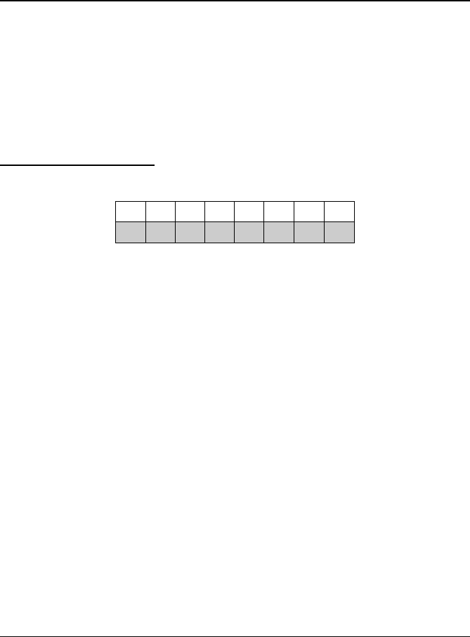
The Fl e g Re g i s t e r c o n s i s t s o f t h e f o l l o wi ng bi t s :
7 6 5 4 3 2 1 0
Z N H C 0 0 0 0
•Ze r o Fl a g ( Z) :
Thi s b i t i s s e t wh e n t he r e s ul t o f a ma t h o p e r a t i o n
is zero or two values match when using the CP
instruction.
•Subt ract Fl ag ( N) :
Thi s b i t i s s e t i f a s ub t r a c t i o n wa s p e r f o r me d i n t he
last math instruction.
•Ha l f C a r r y F l a g ( H) :
Thi s b i t i s s e t i f a c a r r y o c c u r r e d f r o m t he l owe r
ni bbl e i n t he l as t mat h oper at i on.
•Ca r r y F l a g ( C) :
Thi s b i t i s s e t i f a c a r r y o c c u r r e d f r o m t he l a s t
ma t h o p e r a t i o n o r i f r e g i s t e r A i s t h e s ma l l e r v a l u e
wh e n e x e c u t i n g t h e CP i n s t r u c t i o n .
Page 62 V 1.01

Game BoyTM CPU Manual 3.2.3. Program Counter
3.2.3. Program Counter
On power up, the GameBoy Program Counter is
initialized to $100 (100 hex) and the instruction found
at t hi s l ocat i on i n ROM i s execut ed.
The Program Counter from this point on is controlled,
indirectly, by the program instructions themselves that
we r e g e n e r a t e d b y t h e p r o g r a mme r o f t h e ROM c a r t .
3.2.4. Stack Pointer
A b i g k e y t o u n d e r s t a n d i n g p r o g r a mmi n g i n a s s e mb l y
language on the GameBoy is understanding the concept of
a st ack poi nt er . A f ami l i ari t y wi t h assembl y l anguage
for other processors helps greatly as the concepts are
the same.
The GameBoy Stack Pointer is used to keep track of the
top of the "stack". The stack is used for saving
var i abl es , savi ng r et ur n addr esses, passi ng ar gument s
to subroutines, and various other uses that might be
concei ved by t he i ndi vi dual pr ogr ammer.
The i ns t r u c t i o n s CALL, PUSH, a n d RST a l l p u t
information onto the stack. The instructions POP, RET,
and RETI al l t ake i nf or mat i on of f of t he st ack.
(Interrupts put a return address on the stack and
remove it at their completion as well.)
As information is put onto the stack, the stack grows
downwar d i n RAM memor y. As a r esul t , t he St ack Poi nt er
should al ways be i niti al i zed at the hi ghest locati on of
RAM s p a c e t h a t h a s b e e n a l l o c a t e d f o r u s e b y t h e s t a c k .
For i ns t a nce, i f a pr ogr a mmer wi s hes t o l oc a t e t he
St ac k Poi nt er at t he t op of l ow RAM s pac e ( $C000- $DFFF)
he woul d s et t he St ack Poi nt er t o $E000 usi ng t he
by DP Page 63

3.2.4. Stack Pointer Game BoyTM CPU Manual
command LD SP, $E000. ( The St ack Poi nt er aut omat i cal l y
decr ement s bef or e i t put s s omet hi ng ont o t he st ack so
it is perfectly acceptable to assign it a value which
poi nt s t o a memor y addr es s whi ch i s one l ocat i on pas t
the end of available RAM.)
The GameBoy stack pointer is initialized to $FFFE on
power up but a pr ogr ammer shoul d not r el y on t hi s
setti ng and rather shoul d expl icit l y set it s val ue.
Page 64 V 1.01
Game BoyTM CPU Manual 3.3. Commands
3.3. Commands
The Ga me Bo y CPU i s b a s e d o n a subset of the Z80 micro-
pr ocessor . A s ummar y of t hese commands i s gi ven bel ow.
If ' Flags affected' is not given for a command then
none ar e af f ect ed.
3.3.1. 8-Bit Loads
1. LD nn,n
De s c r i p t i o n :
Put value nn into n.
Us e wi t h :
nn = B,C,D,E,H,L,BC,DE,HL,SP
n = 8 bit immediate value
Op c o d e s :
Instruction Parameters Opcode Cycles
LD B,n 06 8
LD C,n 0E 8
LD D,n 16 8
LD E,n 1E 8
LD H,n 26 8
LD L,n 2E 8
by DP Page 65

3.3.1. 8-Bit Loads Game BoyTM CPU Manual
2. LD r1,r2
De s c r i p t i o n :
Put value r2 into r1.
Us e wi t h :
r1,r2 = A,B,C,D,E,H,L,(HL)
Op c o d e s :
Instruction Parameters Opcode Cycles
LD A,A 7F 4
LD A,B 78 4
LD A,C 79 4
LD A,D 7A 4
LD A,E 7B 4
LD A,H 7C 4
LD A,L 7D 4
LD A,(HL) 7E 8
LD B,B 40 4
LD B,C 41 4
LD B,D 42 4
LD B,E 43 4
LD B,H 44 4
LD B,L 45 4
LD B,(HL) 46 8
LD C,B 48 4
LD C,C 49 4
LD C,D 4A 4
LD C,E 4B 4
LD C,H 4C 4
LD C,L 4D 4
LD C,(HL) 4E 8
LD D,B 50 4
LD D,C 51 4
Page 66 V 1.01

Game BoyTM CPU Manual 3.3.1. 8-Bit Loads
LD D,D 52 4
LD D,E 53 4
LD D,H 54 4
LD D,L 55 4
LD D,(HL) 56 8
LD E,B 58 4
LD E,C 59 4
LD E,D 5A 4
LD E,E 5B 4
LD E,H 5C 4
LD E,L 5D 4
LD E,(HL) 5E 8
LD H,B 60 4
LD H,C 61 4
LD H,D 62 4
LD H,E 63 4
LD H,H 64 4
LD H,L 65 4
LD H,(HL) 66 8
LD L,B 68 4
LD L,C 69 4
LD L,D 6A 4
LD L,E 6B 4
LD L,H 6C 4
LD L,L 6D 4
LD L,(HL) 6E 8
LD (HL),B 70 8
LD (HL),C 71 8
LD (HL),D 72 8
LD (HL),E 73 8
LD (HL),H 74 8
LD (HL),L 75 8
LD (HL),n 36 12
by DP Page 67
3.3.1. 8-Bit Loads Game BoyTM CPU Manual
3. LD A,n
De s c r i p t i o n :
Put value n into A.
Us e wi t h :
n = A,B,C,D,E,H,L,(BC),(DE),(HL),(nn),#
nn = two byte immediate value. (LS byte first.)
Op c o d e s :
Instruction Parameters Opcode Cycles
LD A,A 7F 4
LD A,B 78 4
LD A,C 79 4
LD A,D 7A 4
LD A,E 7B 4
LD A,H 7C 4
LD A,L 7D 4
LD A,(BC) 0A 8
LD A,(DE) 1A 8
LD A,(HL) 7E 8
LD A,(nn) FA 16
LD A,# 3E 8
Page 68 V 1.01
Game BoyTM CPU Manual 3.3.1. 8-Bit Loads
4. LD n,A
De s c r i p t i o n :
Put value A into n.
Us e wi t h :
n = A,B,C,D,E,H,L,(BC),(DE),(HL),(nn)
nn = two byte immediate value. (LS byte first.)
Op c o d e s :
Instruction Parameters Opcode Cycles
LD A,A 7F 4
LD B,A 47 4
LD C,A 4F 4
LD D,A 57 4
LD E,A 5F 4
LD H,A 67 4
LD L,A 6F 4
LD (BC),A 02 8
LD (DE),A 12 8
LD (HL),A 77 8
LD (nn),A EA 16
by DP Page 69
3.3.1. 8-Bit Loads Game BoyTM CPU Manual
5. LD A,(C)
De s c r i p t i o n :
Put value at address $FF00 + register C into A.
Same as: LD A,($FF00+C)
Op c o d e s :
Instruction Parameters Opcode Cycles
LD A,(C) F2 8
6. LD (C),A
De s c r i p t i o n :
Put A into address $FF00 + register C.
Op c o d e s :
Instruction Parameters Opcode Cycles
LD ($FF00+C),A E2 8
Page 70 V 1.01
Game BoyTM CPU Manual 3.3.1. 8-Bit Loads
7. LD A,(HLD)
De s c r i p t i o n : Same as: LDD A,(HL)
8. LD A,(HL-)
De s c r i p t i o n : Same as: LDD A,(HL)
9. LDD A,(HL)
De s c r i p t i o n :
Put value at address HL into A. Decrement HL.
Same as: LD A,(HL) - DEC HL
Op c o d e s :
Instruction Parameters Opcode Cycles
LD A,(HLD) 3A 8
LD A,(HL-) 3A 8
LDD A,(HL) 3A 8
by DP Page 71
3.3.1. 8-Bit Loads Game BoyTM CPU Manual
10. LD (HLD),A
De s c r i p t i o n : Same as: LDD (HL),A
11. LD (HL-),A
De s c r i p t i o n : Same as: LDD (HL),A
12. LDD (HL),A
De s c r i p t i o n :
Put A into memory address HL. Decrement HL.
Same as: LD (HL),A - DEC HL
Op c o d e s :
Instruction Parameters Opcode Cycles
LD (HLD),A 32 8
LD (HL-),A 32 8
LDD (HL),A 32 8
Page 72 V 1.01
Game BoyTM CPU Manual 3.3.1. 8-Bit Loads
13. LD A,(HLI)
De s c r i p t i o n : Same as: LDI A,(HL)
14. LD A,(HL+)
De s c r i p t i o n : Same as: LDI A,(HL)
15. LDI A,(HL)
De s c r i p t i o n :
Put va l ue at a ddr e s s HL i nt o A. I ncr e ment HL.
Same as: LD A,(HL) - INC HL
Op c o d e s :
Instruction Parameters Opcode Cycles
LD A,(HLI) 2A 8
LD A,(HL+) 2A 8
LDI A,(HL) 2A 8
by DP Page 73
3.3.1. 8-Bit Loads Game BoyTM CPU Manual
16. LD (HLI),A
De s c r i p t i o n : Same as: LDI (HL),A
17. LD (HL+),A
De s c r i p t i o n : Same as: LDI (HL),A
18. LDI (HL),A
De s c r i p t i o n :
Put A into memory address HL. Increment HL.
Same as: LD (HL),A - INC HL
Op c o d e s :
Instruction Parameters Opcode Cycles
LD (HLI),A 22 8
LD (HL+),A 22 8
LDI (HL),A 22 8
Page 74 V 1.01
Game BoyTM CPU Manual 3.3.1. 8-Bit Loads
19. LDH (n),A
De s c r i p t i o n :
Put A into memory address $FF00+n.
Us e wi t h :
n = one byte immediate value.
Op c o d e s :
Instruction Parameters Opcode Cycles
LD ($FF00+n),A E0 12
20. LDH A,(n)
De s c r i p t i o n :
Put memory address $FF00+n into A.
Us e wi t h :
n = one byte immediate value.
Op c o d e s :
Instruction Parameters Opcode Cycles
LD A,($FF00+n) F0 12
by DP Page 75
3.3.2. 16-Bit Loads Game BoyTM CPU Manual
3.3.2. 16-Bit Loads
1. LD n,nn
De s c r i p t i o n :
Put value nn into n.
Us e wi t h :
n = BC,DE,HL,SP
nn = 16 bit immediate value
Op c o d e s :
Instruction Parameters Opcode Cycles
LD BC,nn 01 12
LD DE,nn 11 12
LD HL,nn 21 12
LD SP,nn 31 12
2. LD SP,HL
De s c r i p t i o n :
Put HL into Stack Pointer (SP).
Op c o d e s :
Instruction Parameters Opcode Cycles
LD SP,HL F9 8
Page 76 V 1.01
Game BoyTM CPU Manual 3.3.2. 16-Bit Loads
3. LD HL,SP+n
De s c r i p t i o n : Same as: LDHL SP,n.
4. LDHL SP,n
De s c r i p t i o n :
Put SP + n effective address into HL.
Us e wi t h :
n = one byte signed immediate value.
Fl ags a f f e ct ed:
Z - Reset.
N - Reset.
H - Set or reset according to operation.
C - Set or reset according to operation.
Op c o d e s :
Instruction Parameters Opcode Cycles
LDHL SP,n F8 12
by DP Page 77
3.3.2. 16-Bit Loads Game BoyTM CPU Manual
5. LD (nn),SP
De s c r i p t i o n :
Put Stack Pointer (SP) at address n.
Us e wi t h :
nn = two byte immediate address.
Op c o d e s :
Instruction Parameters Opcode Cycles
LD (nn),SP 08 20
6. PUSH nn
De s c r i p t i o n :
Push register pair nn onto stack.
Decrement Stack Pointer (SP) twice.
Us e wi t h :
nn = AF,BC,DE,HL
Op c o d e s :
Instruction Parameters Opcode Cycles
PUSH AF F5 16
PUSH BC C5 16
PUSH DE D5 16
PUSH HL E5 16
Page 78 V 1.01
Game BoyTM CPU Manual 3.3.2. 16-Bit Loads
7. POP nn
De s c r i p t i o n :
Pop two bytes off stack into register pair nn.
Increment Stack Pointer (SP) twice.
Us e wi t h :
nn = AF,BC,DE,HL
Op c o d e s :
Instruction Parameters Opcode Cycles
POP AF F1 12
POP BC C1 12
POP DE D1 12
POP HL E1 12
by DP Page 79
3.3.3. 8-Bit ALU Game BoyTM CPU Manual
3.3.3. 8-Bit ALU
1. ADD A,n
De s c r i p t i o n :
Add n to A.
Us e wi t h :
n = A,B,C,D,E,H,L,(HL),#
Fl ags a f f e ct ed:
Z - Set if result is zero.
N - Reset.
H - Set if carry from bit 3.
C - Set if carry from bit 7.
Op c o d e s :
Instruction Parameters Opcode Cycles
ADD A,A 87 4
ADD A,B 80 4
ADD A,C 81 4
ADD A,D 82 4
ADD A,E 83 4
ADD A,H 84 4
ADD A,L 85 4
ADD A,(HL) 86 8
ADD A,# C6 8
Page 80 V 1.01

Game BoyTM CPU Manual 3.3.3. 8-Bit ALU
2. ADC A,n
De s c r i p t i o n :
Add n + Carry flag to A.
Us e wi t h :
n = A,B,C,D,E,H,L,(HL),#
Fl ags a f f e ct ed:
Z - Set if result is zero.
N - Reset.
H - Set if carry from bit 3.
C - Set if carry from bit 7.
Op c o d e s :
Instruction Parameters Opcode Cycles
ADC A,A 8F 4
ADC A,B 88 4
ADC A,C 89 4
ADC A,D 8A 4
ADC A,E 8B 4
ADC A,H 8C 4
ADC A,L 8D 4
ADC A,(HL) 8E 8
ADC A,# CE 8
by DP Page 81

3.3.3. 8-Bit ALU Game BoyTM CPU Manual
3. SUB n
De s c r i p t i o n :
Subtract n from A.
Us e wi t h :
n = A,B,C,D,E,H,L,(HL),#
Fl ags a f f e ct ed:
Z - Set if result is zero.
N - Set.
H - Set if no borrow from bit 4.
C - Set if no borrow.
Op c o d e s :
Instruction Parameters Opcode Cycles
SUB A 97 4
SUB B 90 4
SUB C 91 4
SUB D 92 4
SUB E 93 4
SUB H 94 4
SUB L 95 4
SUB (HL) 96 8
SUB # D6 8
Page 82 V 1.01

Game BoyTM CPU Manual 3.3.3. 8-Bit ALU
4. SBC A,n
De s c r i p t i o n :
Subtract n + Carry flag from A.
Us e wi t h :
n = A,B,C,D,E,H,L,(HL),#
Fl ags a f f e ct ed:
Z - Set if result is zero.
N - Set.
H - Set if no borrow from bit 4.
C - Set if no borrow.
Op c o d e s :
Instruction Parameters Opcode Cycles
SBC A,A 9F 4
SBC A,B 98 4
SBC A,C 99 4
SBC A,D 9A 4
SBC A,E 9B 4
SBC A,H 9C 4
SBC A,L 9D 4
SBC A,(HL) 9E 8
SBC A,# ?? ?
by DP Page 83

3.3.3. 8-Bit ALU Game BoyTM CPU Manual
5. AND n
De s c r i p t i o n :
Logically AND n with A, result in A.
Us e wi t h :
n = A,B,C,D,E,H,L,(HL),#
Fl ags a f f e ct ed:
Z - Set if result is zero.
N - Reset.
H - Set.
C - Reset.
Op c o d e s :
Instruction Parameters Opcode Cycles
AND A A7 4
AND B A0 4
AND C A1 4
AND D A2 4
AND E A3 4
AND H A4 4
AND L A5 4
AND (HL) A6 8
AND # E6 8
Page 84 V 1.01

Game BoyTM CPU Manual 3.3.3. 8-Bit ALU
6. OR n
De s c r i p t i o n :
Logical OR n with register A, result in A.
Us e wi t h :
n = A,B,C,D,E,H,L,(HL),#
Fl ags a f f e ct ed:
Z - Set if result is zero.
N - Reset.
H - Reset.
C - Reset.
Op c o d e s :
Instruction Parameters Opcode Cycles
OR A B7 4
OR B B0 4
OR C B1 4
OR D B2 4
OR E B3 4
OR H B4 4
OR L B5 4
OR (HL) B6 8
OR # F6 8
by DP Page 85

3.3.3. 8-Bit ALU Game BoyTM CPU Manual
7. XOR n
De s c r i p t i o n :
Logical exclusive OR n with register A, result in A.
Us e wi t h :
n = A,B,C,D,E,H,L,(HL),#
Fl ags a f f e ct ed:
Z - Set if result is zero.
N - Reset.
H - Reset.
C - Reset.
Op c o d e s :
Instruction Parameters Opcode Cycles
XOR A AF 4
XOR B A8 4
XOR C A9 4
XOR D AA 4
XOR E AB 4
XOR H AC 4
XOR L AD 4
XOR (HL) AE 8
XOR * EE 8
Page 86 V 1.01
Game BoyTM CPU Manual 3.3.3. 8-Bit ALU
8. CP n
De s c r i p t i o n :
Compare A with n. This is basically an A - n
subtraction instruction but the results are thrown
away.
Us e wi t h :
n = A,B,C,D,E,H,L,(HL),#
Fl ags a f f e ct ed:
Z - Set if result is zero. (Set if A = n.)
N - Set.
H - Set if no borrow from bit 4.
C - Set for no borrow. (Set if A < n.)
Op c o d e s :
Instruction Parameters Opcode Cycles
CP A BF 4
CP B B8 4
CP C B9 4
CP D BA 4
CP E BB 4
CP H BC 4
CP L BD 4
CP (HL) BE 8
CP # FE 8
by DP Page 87
3.3.3. 8-Bit ALU Game BoyTM CPU Manual
9. INC n
De s c r i p t i o n :
Increment register n.
Us e wi t h :
n = A,B,C,D,E,H,L,(HL)
Fl ags a f f e ct ed:
Z - Set if result is zero.
N - Reset.
H - Set if carry from bit 3.
C - Not affected.
Op c o d e s :
Instruction Parameters Opcode Cycles
INC A 3C 4
INC B 04 4
INC C 0C 4
INC D 14 4
INC E 1C 4
INC H 24 4
INC L 2C 4
INC (HL) 34 12
Page 88 V 1.01

Game BoyTM CPU Manual 3.3.3. 8-Bit ALU
10. DEC n
De s c r i p t i o n :
Decrement register n.
Us e wi t h :
n = A,B,C,D,E,H,L,(HL)
Fl ags a f f e ct ed:
Z - Set if reselt is zero.
N - Set.
H - Set if no borrow from bit 4.
C - Not affected.
Op c o d e s :
Instruction Parameters Opcode Cycles
DEC A 3D 4
DEC B 05 4
DEC C 0D 4
DEC D 15 4
DEC E 1D 4
DEC H 25 4
DEC L 2D 4
DEC (HL) 35 12
by DP Page 89
3.3.4. 16-Bit Arithmetic Game BoyTM CPU Manual
3.3.4. 16-Bit Arithmetic
1. ADD HL,n
De s c r i p t i o n :
Add n to HL.
Us e wi t h :
n = BC,DE,HL,SP
Fl ags a f f e ct ed:
Z - Not affected.
N - Reset.
H - Set if carry from bit 11.
C - Set if carry from bit 15.
Op c o d e s :
Instruction Parameters Opcode Cycles
ADD HL,BC 09 8
ADD HL,DE 19 8
ADD HL,HL 29 8
ADD HL,SP 39 8
Page 90 V 1.01

Game BoyTM CPU Manual 3.3.4. 16-Bit Arithmetic
2. ADD SP,n
De s c r i p t i o n :
Add n to Stack Pointer (SP).
Us e wi t h :
n = one byte signed immediate value (#).
Fl ags a f f e ct ed:
Z - Reset.
N - Reset.
H - Set or reset according to operation.
C - Set or reset according to operation.
Op c o d e s :
Instruction Parameters Opcode Cycles
ADD SP,# E8 16
by DP Page 91
3.3.4. 16-Bit Arithmetic Game BoyTM CPU Manual
3. INC nn
De s c r i p t i o n :
Increment register nn.
Us e wi t h :
nn = BC,DE,HL,SP
Fl ags a f f e ct ed:
None.
Op c o d e s :
Instruction Parameters Opcode Cycles
INC BC 03 8
INC DE 13 8
INC HL 23 8
INC SP 33 8
Page 92 V 1.01
Game BoyTM CPU Manual 3.3.4. 16-Bit Arithmetic
4. DEC nn
De s c r i p t i o n :
Decrement register nn.
Us e wi t h :
nn = BC,DE,HL,SP
Fl ags a f f e ct ed:
None.
Op c o d e s :
Instruction Parameters Opcode Cycles
DEC BC 0B 8
DEC DE 1B 8
DEC HL 2B 8
DEC SP 3B 8
by DP Page 93

3.3.5. Miscellaneous Game BoyTM CPU Manual
3.3.5. Miscellaneous
1. SWAP n
De s c r i p t i o n :
Swap upper & lower nibles of n.
Us e wi t h :
n = A,B,C,D,E,H,L,(HL)
Fl ags a f f e ct ed:
Z - Set if result is zero.
N - Reset.
H - Reset.
C - Reset.
Op c o d e s :
Instruction Parameters Opcode Cycles
SWAP A CB 37 8
SWAP B CB 30 8
SWAP C CB 31 8
SWAP D CB 32 8
SWAP E CB 33 8
SWAP H CB 34 8
SWAP L CB 35 8
SWAP (HL) CB 36 16
Page 94 V 1.01
Game BoyTM CPU Manual 3.3.5. Miscellaneous
2. DAA
De s c r i p t i o n :
Decimal adjust register A.
This instruction adjusts register A so that the
correct representation of Binary Coded Decimal (BCD)
is obtained.
Fl ags a f f e ct ed:
Z - Set if register A is zero.
N - Not affected.
H - Reset.
C - Set or reset according to operation.
Op c o d e s :
Instruction Parameters Opcode Cycles
DAA -/- 27 4
3. CPL
De s c r i p t i o n :
Complement A register. (Flip all bits.)
Fl ags a f f e ct ed:
Z - Not affected.
N - Set.
H - Set.
C - Not affected.
Op c o d e s :
Instruction Parameters Opcode Cycles
CPL -/- 2F 4
by DP Page 95
3.3.5. Miscellaneous Game BoyTM CPU Manual
4. CCF
De s c r i p t i o n :
Complement carry flag.
If C flag is set, then reset it.
If C flag is reset, then set it.
Fl ags a f f e ct ed:
Z - Not affected.
N - Reset.
H - Reset.
C - Complemented.
Op c o d e s :
Instruction Parameters Opcode Cycles
CCF -/- 3F 4
5. SCF
De s c r i p t i o n :
Set Carry flag.
Fl ags a f f e ct ed:
Z - Not affected.
N - Reset.
H - Reset.
C - Set.
Op c o d e s :
Instruction Parameters Opcode Cycles
SCF -/- 37 4
Page 96 V 1.01
Game BoyTM CPU Manual 3.3.5. Miscellaneous
6. NOP
De s c r i p t i o n :
No operation.
Op c o d e s :
Instruction Parameters Opcode Cycles
NOP -/- 00 4
7. HALT
De s c r i p t i o n :
Power down CPU until an interrupt occurs. Use this
when ever possible to reduce energy consumption.
Op c o d e s :
Instruction Parameters Opcode Cycles
HALT -/- 76 4
8. STOP
De s c r i p t i o n :
Halt CPU & LCD display until button pressed.
Op c o d e s :
Instruction Parameters Opcode Cycles
STOP -/- 10 00 4
by DP Page 97
3.3.5. Miscellaneous Game BoyTM CPU Manual
9. DI
De s c r i p t i o n :
This instruction disables interrupts but not
immediately. Interrupts are disabled after
instruction after DI is executed.
Fl ags a f f e ct ed:
None.
Op c o d e s :
Instruction Parameters Opcode Cycles
DI -/- F3 4
10. EI
De s c r i p t i o n :
Enable interrupts. This intruction enables interrupts
but not immediately. Interrupts are enabled after
instruction after EI is executed.
Fl ags a f f e ct ed:
None.
Op c o d e s :
Instruction Parameters Opcode Cycles
EI -/- FB 4
Page 98 V 1.01
Game BoyTM CPU Manual 3.3.6. Rotates & Shifts
3.3.6. Rotates & Shifts
1. RLCA
De s c r i p t i o n :
Rotate A left. Old bit 7 to Carry flag.
Fl ags a f f e ct ed:
Z - Se t i f r e s ul t i s z e r o .
N - Reset.
H - Reset.
C - Contains old bit 7 data.
Op c o d e s :
Instruction Parameters Opcode Cycles
RLCA -/- 07 4
2. RLA
De s c r i p t i o n :
Rotate A left through Carry flag.
Fl ags a f f e ct ed:
Z - Set if result is zero.
N - Reset.
H - Reset.
C - Contains old bit 7 data.
Op c o d e s :
Instruction Parameters Opcode Cycles
RLA -/- 17 4
by DP Page 99
3.3.6. Rotates & Shifts Game BoyTM CPU Manual
3. RRCA
De s c r i p t i o n :
Rotate A right. Old bit 0 to Carry flag.
Fl ags a f f e ct ed:
Z - Set if result is zero.
N - Reset.
H - Reset.
C - Contains old bit 0 data.
Op c o d e s :
Instruction Parameters Opcode Cycles
RRCA -/- 0F 4
4. RRA
De s c r i p t i o n :
Rotate A right through Carry flag.
Fl ags a f f e ct ed:
Z - Set if result is zero.
N - Reset.
H - Reset.
C - Contains old bit 0 data.
Op c o d e s :
Instruction Parameters Opcode Cycles
RRA -/- 1F 4
Page 100 V 1.01

Game BoyTM CPU Manual 3.3.6. Rotates & Shifts
5. RLC n
De s c r i p t i o n :
Rotate n left. Old bit 7 to Carry flag.
Us e wi t h :
n = A,B,C,D,E,H,L,(HL)
Fl ags a f f e ct ed:
Z - Se t i f r e s ul t i s z e r o .
N - Reset.
H - Reset.
C - Contains old bit 7 data.
Op c o d e s :
Instruction Parameters Opcode Cycles
RLC A CB 07 8
RLC B CB 00 8
RLC C CB 01 8
RLC D CB 02 8
RLC E CB 03 8
RLC H CB 04 8
RLC L CB 05 8
RLC (HL) CB 06 16
by DP Page 101

3.3.6. Rotates & Shifts Game BoyTM CPU Manual
6. RL n
De s c r i p t i o n :
Rotate n left through Carry flag.
Us e wi t h :
n = A,B,C,D,E,H,L,(HL)
Fl ags a f f e ct ed:
Z - Set if result is zero.
N - Reset.
H - Reset.
C - Contains old bit 7 data.
Op c o d e s :
Instruction Parameters Opcode Cycles
RL A CB 17 8
RL B CB 10 8
RL C CB 11 8
RL D CB 12 8
RL E CB 13 8
RL H CB 14 8
RL L CB 15 8
RL (HL) CB 16 16
Page 102 V 1.01

Game BoyTM CPU Manual 3.3.6. Rotates & Shifts
7. RRC n
De s c r i p t i o n :
Rotate n right. Old bit 0 to Carry flag.
Us e wi t h :
n = A, B, C, D, E, H, L, ( HL)
Fl ags a f f e ct ed:
Z - Set if result is zero.
N - Reset.
H - Reset.
C - Contains old bit 0 data.
Op c o d e s :
Instruction Parameters Opcode Cycles
RRC A CB 0F 8
RRC B CB 08 8
RRC C CB 09 8
RRC D CB 0A 8
RRC E CB 0B 8
RRC H CB 0C 8
RRC L CB 0D 8
RRC (HL) CB 0E 16
by DP Page 103

3.3.6. Rotates & Shifts Game BoyTM CPU Manual
8. RR n
De s c r i p t i o n :
Rotate n right through Carry flag.
Us e wi t h :
n = A,B,C,D,E,H,L,(HL)
Fl ags a f f e ct ed:
Z - Set if result is zero.
N - Reset.
H - Reset.
C - Contains old bit 0 data.
Op c o d e s :
Instruction Parameters Opcode Cycles
RR A CB 1F 8
RR B CB 18 8
RR C CB 19 8
RR D CB 1A 8
RR E CB 1B 8
RR H CB 1C 8
RR L CB 1D 8
RR (HL) CB 1E 16
Page 104 V 1.01

Game BoyTM CPU Manual 3.3.6. Rotates & Shifts
9. SLA n
De s c r i p t i o n :
Shift n left into Carry. LSB of n set to 0.
Us e wi t h :
n = A,B,C,D,E,H,L,(HL)
Fl ags a f f e ct ed:
Z - Set if result is zero.
N - Reset.
H - Reset.
C - Contains old bit 7 data.
Op c o d e s :
Instruction Parameters Opcode Cycles
SLA A CB 27 8
SLA B CB 20 8
SLA C CB 21 8
SLA D CB 22 8
SLA E CB 23 8
SLA H CB 24 8
SLA L CB 25 8
SLA (HL) CB 26 16
by DP Page 105
3.3.6. Rotates & Shifts Game BoyTM CPU Manual
10. SRA n
De s c r i p t i o n :
Shift n right into Carry. MSB doesn't change.
Us e wi t h :
n = A,B,C,D,E,H,L,(HL)
Fl ags a f f e ct ed:
Z - Set if result is zero.
N - Reset.
H - Reset.
C - Contains old bit 0 data.
Op c o d e s :
Instruction Parameters Opcode Cycles
SRA A CB 2F 8
SRA B CB 28 8
SRA C CB 29 8
SRA D CB 2A 8
SRA E CB 2B 8
SRA H CB 2C 8
SRA L CB 2D 8
SRA (HL) CB 2E 16
Page 106 V 1.01

Game BoyTM CPU Manual 3.3.6. Rotates & Shifts
11. SRL n
De s c r i p t i o n :
Shift n right into Carry. MSB set to 0.
Us e wi t h :
n = A,B,C,D,E,H,L,(HL)
Fl ags a f f e ct ed:
Z - Set if result is zero.
N - Reset.
H - Reset.
C - Contains old bit 0 data.
Op c o d e s :
Instruction Parameters Opcode Cycles
SRL A CB 3F 8
SRL B CB 38 8
SRL C CB 39 8
SRL D CB 3A 8
SRL E CB 3B 8
SRL H CB 3C 8
SRL L CB 3D 8
SRL (HL) CB 3E 16
by DP Page 107
3.3.7. Bit Opcodes Game BoyTM CPU Manual
3.3.7. Bit Opcodes
1. BIT b,r
De s c r i p t i o n :
Test bit b in register r.
Us e wi t h :
b = 0 - 7, r = A,B,C,D,E,H,L,(HL)
Fl ags a f f e ct ed:
Z - Set if bit b of register r is 0.
N - Reset.
H - Set.
C - Not affected.
Op c o d e s :
Instruction Parameters Opcode Cycles
BIT b,A CB 47 8
BIT b,B CB 40 8
BIT b,C CB 41 8
BIT b,D CB 42 8
BIT b,E CB 43 8
BIT b,H CB 44 8
BIT b,L CB 45 8
BIT b,(HL) CB 46 16
Page 108 V 1.01
Game BoyTM CPU Manual 3.3.7. Bit Opcodes
2. SET b,r
De s c r i p t i o n :
Set bit b in register r.
Us e wi t h :
b = 0 - 7, r = A,B,C,D,E,H,L,(HL)
Fl ags a f f e ct ed:
None.
Op c o d e s :
Instruction Parameters Opcode Cycles
SET b,A CB C7 8
SET b,B CB C0 8
SET b,C CB C1 8
SET b,D CB C2 8
SET b,E CB C3 8
SET b,H CB C4 8
SET b,L CB C5 8
SET b,(HL) CB C6 16
by DP Page 109

3.3.7. Bit Opcodes Game BoyTM CPU Manual
3. RES b,r
De s c r i p t i o n :
Reset bit b in register r.
Us e wi t h :
b = 0 - 7, r = A,B,C,D,E,H,L,(HL)
Fl ags a f f e ct ed:
None.
Op c o d e s :
Instruction Parameters Opcode Cycles
RES b,A CB 87 8
RES b,B CB 80 8
RES b,C CB 81 8
RES b,D CB 82 8
RES b,E CB 83 8
RES b,H CB 84 8
RES b,L CB 85 8
RES b,(HL) CB 86 16
Page 110 V 1.01
Game BoyTM CPU Manual 3.3.8. Jumps
3.3.8. Jumps
1. JP nn
De s c r i p t i o n :
Jump to address nn.
Us e wi t h :
nn = two byte immediate value. (LS byte first.)
Op c o d e s :
Instruction Parameters Opcode Cycles
JP nn C3 12
2. JP cc,nn
De s c r i p t i o n :
Jump to address n if following condition is true:
cc = NZ, Jump if Z flag is reset.
cc = Z, Jump if Z flag is set.
cc = NC, Jump if C flag is reset.
cc = C, Jump if C flag is set.
Us e wi t h :
nn = two byte immediate value. (LS byte first.)
Op c o d e s :
Instruction Parameters Opcode Cycles
JP NZ,nn C2 12
JP Z,nn CA 12
JP NC,nn D2 12
JP C,nn DA 12
by DP Page 111
3.3.8. Jumps Game BoyTM CPU Manual
3. JP (HL)
De s c r i p t i o n :
Jump to address contained in HL.
Op c o d e s :
Instruction Parameters Opcode Cycles
JP (HL) E9 4
4. JR n
De s c r i p t i o n :
Add n to current address and jump to it.
Us e wi t h :
n = one byte signed immediate value
Op c o d e s :
Instruction Parameters Opcode Cycles
JR n 18 8
Page 112 V 1.01
Game BoyTM CPU Manual 3.3.8. Jumps
5. JR cc,n
De s c r i p t i o n :
If following condition is true then add n to current
address and jump to it:
Us e wi t h :
n = one byte signed immediate value
cc = NZ, Jump if Z flag is reset.
cc = Z, Jump if Z flag is set.
cc = NC, Jump if C flag is reset.
cc = C, Jump if C flag is set.
Op c o d e s :
Instruction Parameters Opcode Cycles
JR NZ,* 20 8
JR Z,* 28 8
JR NC,* 30 8
JR C,* 38 8
by DP Page 113
3.3.9. Calls Game BoyTM CPU Manual
3.3.9. Calls
1. CALL nn
De s c r i p t i o n :
Push address of next instruction onto stack and then
jump to address nn.
Us e wi t h :
nn = two byte immediate value. (LS byte first.)
Op c o d e s :
Instruction Parameters Opcode Cycles
CALL nn CD 12
Page 114 V 1.01
Game BoyTM CPU Manual 3.3.9. Calls
2. CALL cc,nn
De s c r i p t i o n :
Call address n if following condition is true:
cc = NZ, Call if Z flag is reset.
cc = Z, Call if Z flag is set.
cc = NC, Call if C flag is reset.
cc = C, Call if C flag is set.
Us e wi t h :
nn = two byte immediate value. (LS byte first.)
Op c o d e s :
Instruction Parameters Opcode Cycles
CALL NZ,nn C4 12
CALL Z,nn CC 12
CALL NC,nn D4 12
CALL C,nn DC 12
by DP Page 115
3.3.10. Restarts Game BoyTM CPU Manual
3.3.10. Restarts
1. RST n
De s c r i p t i o n :
Push present address onto stack.
Jump to address $0000 + n.
Us e wi t h :
n = $00, $08, $10, $18, $20, $28, $30, $38
Op c o d e s :
Instruction Parameters Opcode Cycles
RST 00H C7 32
RST 08H CF 32
RST 10H D7 32
RST 18H DF 32
RST 20H E7 32
RST 28H EF 32
RST 30H F7 32
RST 38H FF 32
Page 116 V 1.01
Game BoyTM CPU Manual 3.3.11. Returns
3.3.11. Returns
1. RET
De s c r i p t i o n :
Pop two bytes from stack & jump to that address.
Op c o d e s :
Instruction Parameters Opcode Cycles
RET -/- C9 8
2. RET cc
De s c r i p t i o n :
Return if following condition is true:
Us e wi t h :
cc = NZ, Return if Z flag is reset.
cc = Z, Return if Z flag is set.
cc = NC, Return if C flag is reset.
cc = C, Return if C flag is set.
Op c o d e s :
Instruction Parameters Opcode Cycles
RET NZ C0 8
RET Z C8 8
RET NC D0 8
RET C D8 8
by DP Page 117

3.3.11. Returns Game BoyTM CPU Manual
3. RETI
De s c r i p t i o n :
Pop two bytes from stack & jump to that address then
enable interrupts.
Op c o d e s :
Instruction Parameters Opcode Cycles
RETI -/- D9 8
Page 118 V 1.01

Game BoyTM CPU Manual 4. Super Game Boy commands
4. Super Game Boy commands
4.1. Foreword
Super GameBoy Commands , Ext ract ed by kOOPa, 15- Feb- 98
-----------------------------------------------------
Las t updat ed by: Bows e r , 1 3- J u n e - 9 8
Up d a t e s :
Bl o c k Ar e a mo d e ( $ 0 4 ) c o n t r o l c o d e s u p d a t e d
Li n e mo d e ( $ 0 5 ) wr i t t e n
Di v i d e mo d e ( $ 0 6 ) wr i t t e n
1CHR mode ( $07) wr i t t en
A SGB command transfer is 128 bits + a zero bit. The
first five bits of the first byte is the command byte.
The l a s t 3 bi t s o f t he f i r s t b y t e r e p r e s e n t t h e nu mb e r
of 128 bi t packages t o be s ent . Unus ed bi t s i n a SGB
command t r ansfer shoul d be set t o 0.
Most of the commands listed below only transfer one
package. The command byt es bel ow ar e pr eceded by t he #
charact er t o r emi nd you t hat t hey have t o be shi f t ed
left three times before used.
4.2. Palettes
There are several different types of palettes in the
SGB. One t ype i s t he Sys t em col or pa l et t e. I t i s a
vi r t ual pal et t e r at her t han a har dwar e pal et t e. The
har dwar e col or pal et t e i s shown at t he bot t om of t hi s
document and cont ai ns what ar e cal l ed t he SGB col or
pal et t es and al so hol ds t he SGB Bor der pal et t e.
As far as SGB onscreen colors are concerned there are
onl y r eal l y t wo pal et t e t ypes: SGB col or pal et t es and
by DP Page 119

4.2. Palettes Game BoyTM CPU Manual
the SGB border palette.
The SGB border palette is setup using command $14.
The r e a r e 64 c o l or s i n t h i s p a l e t t e .
The SGB color palettes may be set directly using
commands $00-$03. There are a t ot al of f our of
these palettes and they determine which colors are
used i n t he mai n game act i on wi ndow. The col or f or
bi t 00 wi l l be t he same f or al l SGB col or pal et t es.
The c o l o r mo s t r e c e n t l y s t or e d i n b i t 00 wi l l b e us e d .
The SGB color palettes may be set indirectly using
the System color palettes using commands $0a-$0b.
The r e a r e a t ot a l o f 5 1 2 o f t he s e pa l e t t e s .
4.3. SGB Border
The SGB border is often shown as colorful graphics
that surround the main game action window. The truth is
that the SGB border actually covers the whole viewing
screen and has the hi ghest viewi ng priori ty. The reason
it appears be just a "border" around most games is due
to the fact that usually a 160x144 pixel wide box is
dr awn i n t he cent er of t he SGB "bor der " usi ng col or 0.
Si nc e t hi s col or i s t r a ns par e nt , t he ma i n ga me a ct i on
wi n d o w u n d e r i t i s v i s i b l e .
Creating a program to convert a 16-color GIF to a SGB
bor der i s r el at i vel y eas y and has been done f or DOS.
(i.e.gif2sopt.exe) What is not so easy is converting a
64- col or GI F t o a SGB bor der becaus e each t i l e onl y has
access t o 16- col or s. The 16- col or pal et t e t hat t he t i l e
has access t o i s det er mi ned by t he t i l e at t r i but e byt e.
The t i l e a t t r i but e by t e i s d e s c r i be d i n t he ' Pi c t ur e
Tr a ns f e r ' c o mma n d ( $ 1 4 ) b e l ow.
Page 120 V 1.01

Game BoyTM CPU Manual 4.4. Main Action Window
4.4. Main Action Window
The SGB cartridge that plugs into the SNES contains
a GB CPU. The SNES i s abl e t o vi deo capt ur e t he vi deo
out put of t hi s GB CPU and di spl ay i t on t he s cr een as
the main game action window. Since the SNES is only
doi ng a r aw vi deo capt ur e i t onl y knows about 4 l evel s
of gr ey comi ng f r om t he GB CPU. I n or der t o add mor e
than 4 colors to the main game action window, the SGB
soft ware al lows you t o assi gn 1 of the 4 SGB col or
pal et t es f or each 8x8 t i l e posi t i on i n t hi s wi ndow.
"Bl ock"($4), "Li ne"($5), "Di vi de"($6), "1Chr"($7),
and "Set At t r fr om ATF"( $15) al l ar e di f ferent means
for setting the palettes for each 8x8 tile location.
On r e s e t , e a c h 8 x 8 t i l e p o s i t i o n d e f a u l t s t o S GB
col or pal et t e 0.
Commands $4-$7 are various methods for block-setting
the 8x8 tile color palettes. The "Set Attr from ATF"
($15) allows you to select 1 of 45 "ATtribute Files".
Ea c h " ATt r i b u t e Fi l e " c ont a i n s 9 0 byt e s ( 2 0 x18 x 2 bi t s ) .
By s e l e c t i n g a n " ATt r i b u t e F i l e " , y o u c a n e x a c t l y
select 1 of 4 SGB color pal et tes for each 8x8 t ile
location due to the fact that these files contain
2 bi t s of i nf or mat i on f or each 8x8 t i l e l ocat i on.
by DP Page 121

4.5. Commands Game BoyTM CPU Manual
4.5. Commands
1. Set SGB color Palettes
0 & 1 ($00,data) - Download color palettes 0 & 1
2 & 3 ($01,data) - Download color palettes 2 & 3
0 & 3 ($02,data) - Download color palettes 0 & 3
1 & 2 ($03,data) - Download color palettes 1 & 2
--------------------------------------------------
He r e i s e x a mp l e d a t a f o r s e t t i n g S GB c o l o r
pal et t es 0 & 1:
DW $7fff ;white ;bit 00 color
;Pallete 0
DW $7c00 ;blue ;bit 01 color
DW $03e0 ;green ;bit 10 color
DW $0000 ;black ;bit 11 color
;Palette 1
DW $03ff ;yellow ;bit 01 color
DW $001f ;red ;bit 10 color
DW $0000 ;black ;bit 11 color
Please note that all four SGB color palettes share the
same bi t 00 color. The col or most recentl y st ored in
bi t 00 wi l l be us ed.
Information for calculating the DW color value is
gi ven l at er i n t hi s t ext .
When using the following four Palette Direct Set
commands, t he GameBoy i mage wi l l be al t er ed ( col or s
changed) even i f you used t he GameBoy Wi ndow Mask
command t o f reeze t he scr een. Ther efore use ar gument s
Page 122 V 1.01

Game BoyTM CPU Manual 4.5. Commands
Bl a c k o r Wh i t e wi t h t h e Wi n d o w Ma s k c o mma n d b e f o r e
usi ng t he f ol l owi ng f our commands. I f you want t o
freeze the screen, send palette data with the Attribute
Fi l e ATF0- ATF44. I n t he e vent you ar e changi ng t he
screen by sendi ng at tri bute dat a and col or data at t he
same t i me, use Set SGB Pal ette Indi rect command.
2. "Block" Area Designation Mode ($04)
(other data shown below)
$00 - %00100xxx
xxx = # of packets
$01 - %///xxxxx
xxxxx = # of data sets - One data set is control
code, color palette designation, & the coords.
$02 - %/////xxx
xxx = Control code
000 = don' t car e
001 = s et pal ( i ns i de bl ock + s ur r oundi ng
block line) to 'zz' of $03
010 = s et pal of s ur r oundi ng bl ock l i ne t o
'yy' of $03
011 = s et pal i ns i de bl ock t o ' yy' &
surrounding block line to 'yy'
100 = s et pal out s i de t he bl ock t o ' xx'
101 = s et pal i ns i de t o ' zz' & out s i de t he
block to 'xx'
110 = s et pal out s i de t he bl ock t o ' xx'
111 = s et pal i ns i de bl ock t p ' zz' +
surrounding line to 'yy' + outside block
to 'xx'
by DP Page 123

4.5. Commands Game BoyTM CPU Manual
$03 - %//xxyyzz
Color Palette Designation
xx = col or pal et t e out si de s ur r ounded ar ea
yy = col or pal et t e on sur r oundi ng bl ock l i ne
zz = col or pal et t e i nsi de surrounded ar ea
$04 - %///xxxxx xxxxx = start point H
$05 - %///xxxxx xxxxx = start point V
$06 - %/ / / xxxxx xxxxx = end point H
$07 - %///xxxxx xxxxx = end point V
$08-$0d Repeat of $02-$07 data if # of data sets > 1.
If number of packets is 1, set $0e & $0f to $00.
3. "Line" Area Designation Mode ($05)
$00 - %00101xxx
xxx = # packets
$01 - %xxxxxxxx
number of data sets ($1 - $6E), one data set
controls: code, colours palette designation, and
coords.
$02 - %xyyzzzzz
control code 1'st data set
x = Mode (0 = Horizontal line, 1 = Vertical line)
yy = Palette number
zzzzz = Line number
On e d a t a s e t i s 1 b y t e j u s t a s $ 0 2 . I f # d a t a s e t s = 1 ,
fill with 0' s up to $0F.
Page 124 V 1.01

Game BoyTM CPU Manual 4.5. Commands
4. "Divide" Area Designation Mode ($06)
$00 - %00101001
(number of packets must be 1)
$01 - %/vxxyyzz
control code
v = Mode ( 0 = di vi de hor i z ont al l y,
1 = Divide vertical)
xx = Col our pal e t t e ON di vi s i on l i ne
yy = Col our pal e t t e ABOVE & LEFT of di vi s i on
zz = col our pa l e t t e BELOW & RI GHT of di vi s i on
$02 - %///xxxxx
xxxxx = Character line number to divide at fill with
0's to $0F
5. "1CHR" Area Designation Mode ($07)
$00 - %00111xxx
xxx = number of packet s ( $01 - $06)
$01 - %///xxxxx
Be g i n n i n g X c o o r d i n a t e
$02 - %///yyyyy
Be g i n n i n g Y c o o r d i n a t e
$03 - %xxxxxxxx
Nu mb e r o f d a t a s e t s , 2 b i t s = 1 d a t a s e t
$04 - %///////x
MS B o f d a t a i n $ 0 3 . Ma x n u m b e r = 3 6 0 .
$05 - %///////x
by DP Page 125

4.5. Commands Game BoyTM CPU Manual
Wr i t i n g s t y l e ( 0 = L e f t - > r i g h t , 1 = u p - >
down)
$06 - %vvxxyyzz dat a
vv = pal f or dat as et 1
xx = pal f or dat as et 2
yy = pal f or dat as et 3
zz = pal f or dat aset 4
$07 - %vvxxyyzz dat a
et c. . .
6. Sound On/Off ($08)
7. Transfer Sound PRG/DATA ($09)
This transfers your score (in .GAK format) data.
Set SGB Palette Indirect ($0a)
Page 126 V 1.01
Game BoyTM CPU Manual 4.5. Commands
8. Set System Color Palette Data ($0b)
9. Enable/Disable Attraction Mode ($0c)
10. Speed Function ($0d)
11. SGB Function ($0e)
12. Super NES WRAM Transfer 1 ($0f)
13. Super NES WRAM Transfer 2 ($10)
14. Controller 2 Request (#11) ($00) - Request 1 play
15. Controller 2 Request (#11) ($01) - Request 2 play
Is used to determine if system is SGB or regular GB.
16. Set Program Counter ($12)
17. CharSet Transfer ($13)
(%00000xyy) (x=Char Type:0=BG,1=OBJ y=CharSet
Range:0=00-7f,1=80-ff)
The tiles that are downloaded to the SNES for the
bor der ar e r egul ar GB t i l es t hat have been modi f i ed f or
ext ra col ors. Every t i l e consi st s of 32 byt es. The
format is:
16 bytes - Standard 4 color GB character set
16 bytes - Extended color information
The same way GB uses two bytes to convey 8 pixels
and t he 4 col or s f or each pi xel , t he ext ended col or
by DP Page 127

4.5. Commands Game BoyTM CPU Manual
info uses the same technique for determining extended
col or s. Thi s t el l s t he SNES whi ch col or pal et t e t o
use t o di s pl ay each pi xel . Thi s al l ows a t ot al of 16
col or s per t i l e. Si nce SGB bor der s suppor t up t o 64
col or s, access t o t he ot her col or s ar e achi eved by
changi ng t he Maj or pal et t e number i n t he pi ct ur e
transfer tile map.
Page 128 V 1.01

Game BoyTM CPU Manual 4.5. Commands
18. Picture Transfer ($14) - Download border to SNES.
The border (or tile map) that is downloaded is 32x28
tiles or 256x224 pixels. The regular GB screen fits
right in the middle like this:
XXXXXXXXXXXXXXXXXXXXXXXXXXXXXXXX
XXXXXXXXXXXXXXXXXXXXXXXXXXXXXXXX
XXXXXXXXXXXXXXXXXXXXXXXXXXXXXXXX
XXXXXXXXXXXXXXXXXXXXXXXXXXXXXXXX
XXXXXXXXXXXXXXXXXXXXXXXXXXXXXXXX
XXXXXX....................XXXXXX
XXXXXX....................XXXXXX
XXXXXX....................XXXXXX
XXXXXX....................XXXXXX
XXXXXX....................XXXXXX
XXXXXX....................XXXXXX
XXXXXX....................XXXXXX
XXXXXX....................XXXXXX
XXXXXX....................XXXXXX
XXXXXX....................XXXXXX
XXXXXX....................XXXXXX
XXXXXX....................XXXXXX
XXXXXX....................XXXXXX
XXXXXX....................XXXXXX
XXXXXX....................XXXXXX
XXXXXX....................XXXXXX
XXXXXX....................XXXXXX
XXXXXX....................XXXXXX
XXXXXXXXXXXXXXXXXXXXXXXXXXXXXXXX
XXXXXXXXXXXXXXXXXXXXXXXXXXXXXXXX
XXXXXXXXXXXXXXXXXXXXXXXXXXXXXXXX
XXXXXXXXXXXXXXXXXXXXXXXXXXXXXXXX
XXXXXXXXXXXXXXXXXXXXXXXXXXXXXXXX
by DP Page 129

4.5. Commands Game BoyTM CPU Manual
The tile map consists of a tile number byte & a tile
at t ri but e byt e at each posi t i on on t he map. A t ot al of
32 l i nes ar e downl oaded even t hough t he l ast 4 l i nes
are not vi si bl e. Thi s woul d equal 64 byt es per l i ne and
a t ot al of 2048 byt es per map. Next , a 64 x 2 byt e
col or pal et t e f or t he map i s downl oaded. The f i r st
pal et t e ent r y col or i s t r ans par ent . Use t hi s col or t o
di spl ay r egul ar GB s cr een under neat h.
The tile number comes before the tile attribute of
each posi t i on. Ther e can be up t o 1024 t i l es f r om whi ch
to select. The SGB only supports 256 so bits 0 & 1 of
the tile attribute must be set to 0. Here are the tile
at t ri but es I under st and so f ar:
Bi t 7 - Ve r t i c a l f l i p t i l e
Bi t 6 - Ho r i z o n t a l f l i p t i l e
Bi t 5 - Do e s n o t h i n g ( Se t t o 0 . )
Bi t 4 - S e l e c t Ma j o r Pa l e t t e MSB ( Us u a l l y s e t t o 1 . )
Bi t 3 - S e l e c t Ma j o r Pa l e t t e -
Bi t 2 - S e l e c t Ma j o r Pa l e t t e LSB
Bi t 1 - Ti l e # MS B ( Mo s t s i g n i f i c a n t b i t ) ( Se t t o 0 . )
Bi t 0 - Ti l e # NS B ( Ne x t mo s t s i g n i f i c a n t b i t ) ( S e t t o
0.)
This is often called the SGB border but in fact it
covers t he whol e SNES screen. The Maj or Pal et t e sel ect
has 8 di f f er ent set t i ngs . Onl y t he l ast 4 - 7 ar e
nor mal l y us ed t hought t o acces s al l 64 col or s
transfered with cmd (#14).
(NOTE: If using ' gif2sopt.exe' to generate a border,
the range of the palette selections is 1-8 so select
pal et t e 5 s i nce t hat pr ogr am onl y al l ows up t o 16
col ors. )
Page 130 V 1.01

Game BoyTM CPU Manual 4.5. Commands
19. Set Attribute from ATF ($15)
The data for 45 Attribute files is transfered with
this command. Each ATtribute File is 90 bytes so
90x45 or 4050 bytes of data are transfered. Each
attribute file uses 5 bytes per 8x8 horizontal
line (20 x 4 char/byte x 2 bits/palette) to
describe the color palettes of a line.
Example ATF data:
DB $ff,$00,$00,$00,$02 ; Line #1
DB $ff,$00,$00,$00,$02 ; Line #2
DB $ff,$00,$00,$00,$02 ; Line #3
.....
DB $ff,$00,$00,$00,$02 ; Line #18
The above ATtribute File would set the SGB color
palette selection to 3 for the first 4 columns
of the main game action window. The last column
would have SGB color palette 2 selected. All the
other columns would have palette 0 selected.
20. Set Data from ATF ($16) (data)
Transfer specified ATtribute File to GameBoy window.
data:
%/xyyyyyy
x - 0 = No Change, 1 = Cancel mask after xfer ATF
yyyyyy = ATtribute File number ($00-$2c)
21. GameBoy Window Mask ($17) (data)
data:
$00 = Off
$01 = Transfers VRAM to SNES until cancelled.
by DP Page 131

4.5. Commands Game BoyTM CPU Manual
$02 = Mask so that all color codes in SGB
color palette are black.
$03 = Mask so that all color codes in SBG
color palette are white.
22. Super NES OBJ Mode ($18)
23. SNES Color Palette Info
The Nintendo Super Famicom is capable of displaying
256 col or s f r om a pal et t e of 32, 768. These 256 col or s
are spl i t i nt o 16 pal et t es of 16 col or s each. Onl y 8 of
these palettes are accessible by the SGB.
Co l o r d a t a i s ma d e u p o f 3 c o mp o n e n t s ( Re d , Gr e e n , Bl u e )
each of 5 bi t s (The Ami ga uses exact l y t he same syst em,
but onl y usi ng 4 bi t s per component ) .
00000 00000 00000
\ / \ / \ /
\ / \ / \ /
B G R
Ex a mpl e s :
00000 10111 11100
11111 00000 00000 = $7C00 (Bright Blue)
00000 11111 00000 = $03E0 (Bright Green)
00000 00000 11111 = $001F (Bright Red)
00000 00000 00000 = $0000 (Black)
11111 11111 11111 = $7FFF (White)
Page 132 V 1.01

Game BoyTM CPU Manual 4.5. Commands
24. SGB Palette Selection
There is actually only one color palette in the SNES
but i t i s di vi ded up i nt o s ever al s ect i ons f or
di f f er ent SGB f unct i ons. These s ect i ons ar e r ef er r ed t o
as Maj or ( M) sect i ons 0- 7. Some SGB f unct i ons even
di vi ded s ome of t hese s ect i ons i nt o s ect i ons . These
sections are referred t o as mi nor (m) sect ions. The
large blocks below represent Major sections or palettes
and smal l er ones bel ow t hem r epr esent mi nor pal et t es.
The r e a r e 4 c ol o r s p e r mi n o r pa l e t t e a n d 1 6 c ol o r s p e r
Ma j o r p a l e t t e :
+----+----+----+----+----+----+----+----+
| 0 | 1 | 2 | 3 | 4 | 5 | 6 | 7 |
+----+----+----+----+----+----+----+----+
|0123| ^ ^
+----+ | |
^ ^ +- - - - - - - - +- - - - - - - - +
+--+-+ |
| |
Set wi t h Comma nds Set wi t h 64 c ol or s i n Pi ct ur e
#00, #01, #02, & #03 Tr ans f er ( #14)
(holds SGB Border colors)
by DP Page 133

5. Appendix A Game BoyTM CPU Manual
5. Appendix A
5.1. Emulator Notes
No t e s f o r g e t t i n g a s s e mb l y l a n g u a g e p r o g r a ms t h a t r u n
on an emul at or t o r un on a r eal GB ( by kOOPa, 2- Jan- 98)
1. Emul a t o r s t e n d t o s e t a l l of RAM t o $ 00 o n p o we r up.
Re a l GBs d o NOT i n i t i a l i z e RAM o n p o we r u p . RAM i s
filled with random values on power up. You must clear
it yourself if you wish it to be set to some known
val ue.
2. The r e a l h a r d wa r e c oul d c a r e l e s s a b out t he ROM
checksum ( $14e, $14f ) but t he compl ement check ( $14d)
MU S T b e c o r r e c t o r p r o g r a m s w i l l " l o c k u p " a f t e r
scrol ling t he Ni ntendo l ogo.
Use RGBFIX -V in the RGBDS development system to set
the checksum and the complement byte after each
source code compi l e. It doesn' t matt er whet her you
pr ogr am i n C or assembl y, t hi s pr ogr am wi l l f i x i t .
3. The Ni nt e n do s c r o l l i n g g r a p hi c f r o m $1 0 4 - $1 33 mu s t
be accur at e. I f one byt e of i t i s changed t hen your
pr ogr ams wi l l "l ock up" af t er s cr ol l i ng t hi s gr aphi c
l ogo.
4. Wh e n t h e L C D d i s p l a y i s o f f ( b i t 7 o f $ f f 4 0 s e t t o 0 )
you can wr i t e t o vi deo memor y at any t i me wi t h out
restrictions. While it is on you can only write to
vi deo memor y dur i ng H- Bl ank and V- Bl ank. Code s i mi l ar
to this will work:
; Write B to Video RAM location HL
WriteVRAM:
di ;turn off interrupts
Page 134 V 1.01

Game BoyTM CPU Manual 5.1. Emulator Notes
Write1:
ldh a,[$41] ;read $ff41
and 2
jr nz,Write1
ld [hl],b
ei ;turn on interrupts
ret
The r e s ho u l d no t b e ma ny i ns t r uc t i on s b e t we e n t he " j r
nz" and wr i t e t o memor y "l d [ hl ] , b". A wor s t case of
64 CPU cl ock cycl es ar e avai l abl e t o access mai n
vi deo memor y ( not OAM! ) f ol l owi ng t he "j r nz"
command.
The "di" and "ei" commands above are only required
if you are using Serial, Timer, or Hi-2-Lo
interrupts.
5. The LCD di s pl a y i s on a t r e s e t ( b i t 7 of $ f f 4 0 s e t t o
bi t 7 of $f f 40 set t o 1) . Bef or e t he LCD di s pl ay can
be t ur ned of f you must wai t f or V- Bl ank. One popul ar
wa y o f d o i n g t h i s i s t h e f o l l o wi n g :
; Turn off LCD display
LCDOff:
ldh a,[$44h] ; $ff44=LCDC Y-Pos
cp $90 ; $90 and bigger = in VBL
jr nz,LCDOff ; Loop until = $90
xor a
ldh [$41],a ; Turn off LCD display
ret
No t e y o u s h o u l d d i s a b l e i n t e r r u p t s , i f t h e y a r e
enabl ed, bef ore execut i ng t he above code or el se t he
test of $ff44 could prove invalid.
Tur ni n g t he LCD di s pl a y on c a n be done a t a n y t i me .
by DP Page 135

5.1. Emulator Notes Game BoyTM CPU Manual
6. If you are using sprites then you should not use the
following commands when their register contents are
in the range $fe00-$feff.
inc bc
inc de
inc hl
dec bc
dec de
dec hl
If you don' t follow this rule, sprite trash in the
form of sprite "blink" will randomly affect your
spri tes.
7. No r ma l l y y o u s h o u l d o n l y ma k e c h a n g e s t o S p r i t e RAM
dur i ng V- Bl ank unl es s you ar e an exper t and know
exact l y what you ar e doi ng. The common way t o do t hi s
is to use the GB DMA register ($ff46) to do a fast
copy from your spr i t e t abl e i n RAM t o $f E00- $f e9f .
A. Yo u n e e d a s p r i t e t a b l e i n RAM wi t h a s t a r t i n g
address of $XX00 and wi t h a l engt h of 160 ( $a0) . Many
of t en us e $c000- $c09f f or t hi s pur pose but anywher e
in RAM starting with $XX00 is fine.
B. Yo u n e e d t o c r e a t e a VBl a n k i n t e r r u p t r o u t i n e t h a t
cont ai ns t he DMA command, f ol l owed by a shor t del ay
to allow the DMA to complete, and copy this routine
to high RAM ($ff00-$fffe). The DMA command WILL NOT
WO R K i n R O M o r l o w R A M b e c a u s e t h e s e a r e d i s a b l e d
dur i ng DMA.
C. Af t e r c o p y i n g t h i s r o u t i n e t o h i g h RAM y o u t h e n n e e d
to enable the VBLANK interrupt and then enable
interrupts.
Page 136 V 1.01
Game BoyTM CPU Manual 5.2. Typical timing diagram
5.2. Typical timing diagram
(Based on an email from Philippe Pouliquen)
The g r a p hi c s ho ws a wr i t e f o l l o we d b y t wo r e a d s
(measured on a regular GameBoy):
Ti mi ng:
a: 0ns
this is the point at which CLK goes high, from which
the other times are measured.
b: 140ns
point at which /RD will rise before a write. This is
also the point at which the address on the address
bus changes.
c: 240ns
point at which /CS goes low (this is pin 5 of the
connector)
d: 480ns
point at which CLK goes low. This is also the point
at which /WR goes low for a write and the GameBoy
starts driving the data bus.
e: 840ns
by DP Page 137
_________ _________ _________ ___
CLK: ____/ \ _________ / \_________/ \_________/
_________________
/RD:_______/ \__________________________________________
______________ _____________________________________________
/WR: \ _______/
__________ _____ _____ ___
/CS: \_____________/ \ _____________/ \ _____________/
Ad r : _______ ___________________ ___________________ __________________ _
Bus : _______X___________________X___________________X__________________X_
Dt a : ________ _ _________ _________
Bus : --------------<________ _ >- --------<_________>---------<_________>- - -
^ ^ ^ ^ ^ ^^
Ti me : a b c d e fg

5.2. Typical timing diagram Game BoyTM CPU Manual
point at which /WR goes high after a write.
f: 960ns
point at which CLK goes high. This is also the point
at which /CS goes high and the GameBoy stops
driving the data bus.
g: 990ns
point at which /RD goes low for a read (30ns after
CLK goes high).
(Measurements roundet to the nearest 10ns)
"Some devi ces (l i ke di sk cont rol l er chi ps) requi re t hat
the address be valid before you access them (with a
read or write pulse).
The problem is that /RD doesn't go high between
consecut i ve r eads, and t he second probl em i s t hat when
/RD transitions, it does so at the same time (or
bef or e) t he addr es s changes. The r esul t i s t hat f r om
the device's perspective, an address transition looks
like a bunch of reads from random addresses. These
spuri ous reads are ok for RAM and ROM, but can real l y
screw things up for devices wi t h internal buffers,
becaus e t hey may be f ool ed i nt o t hi nki ng t hat you have
read more data from them than you actually have.
The wa y t o s o l ve t h i s pr o b l e m i s t o f e e d CLK a n d / RD
through a OR gate. The downside is that it makes your
al l owabl e r ead t i me shor t er.
Page 138 V 1.01

C O M M A N D I N D E X Game BoyTM CPU Manual
Co mma n d P a g e
ADC A, n 81
ADD A, n 80
ADD HL , n 90
ADD S P , n 91
AND n 84
BI T b , r 108
CALL c c , n n 115
CALL n n 114
CCF 96
CPL 95
CP n 87
DAA 95
DE C n 89
DE C n n 93
DI 98
EI 98
HALT 97
INC n 88
INC nn 92
JP (HL) 112
JP cc, nn 111
JP nn 111
JR cc, n 113
JR n 112
LD ( C) , A 70
LD ( HL+) , A 74
Co mma n d P a g e
LD ( HL- ) , A 72
LD ( HLD) , A 72
LD ( HLI ) , A 74
LD ( n n ) , SP 78
LD A, ( C) 70
LD A, ( HL+) 73
LD A, ( HL- ) 71
LD A, ( HLD) 71
LD A, ( HLI ) 73
LD A, n 68
LDD ( HL) , A 72
LDD A, ( HL) 71
LDH ( n ) , A 75
LDH A, ( n ) 75
LDI ( HL) , A 74
LDI A, ( HL) 73
LD n , A 69
LD n , nn 76
LD n n , n 65
LD r 1 , r 2 66
LD SP, HL 76
NOP 97
OR n 85
POP nn 79
PUSH nn 78
RES b , r 110
Co mma n d P a g e
RET 117
RET c c 117
RETI 118
RLA 99
RLCA 99
RLC n 101
RL n 102
RRA 100
RRCA 100
RRC n 103
RR n 104
RST n 116
SBC A, n 83
SCF 96
SET b, r 109
SLA n 105
SRA n 106
SRL n 107
STOP 97
SUB n 82
SWAP n 94
XOR n 86
LD HL, SP+n 77
LDHL SP, n 77
by DP Page 139