Phychips PRM90U10A UHF RFID READER HYBRID MODULE User Manual User s Menuals x
Phychips Inc. UHF RFID READER HYBRID MODULE User s Menuals x
Phychips >
USERS MANUAL

USER’S MANUAL
December 2010

9 December 2010 2 of 13
PRM90U10A Specification- Preliminary Version
Contents
1 Overview & block composition diagram................................................... 3
2 Pin Description ............................................................................................ 4
3 Operation method........................................................................................ 6
4 Specification ……………………………………………………………………..12
9 December 2010 3 of 13
PRM90U10A Specification- Preliminary Version
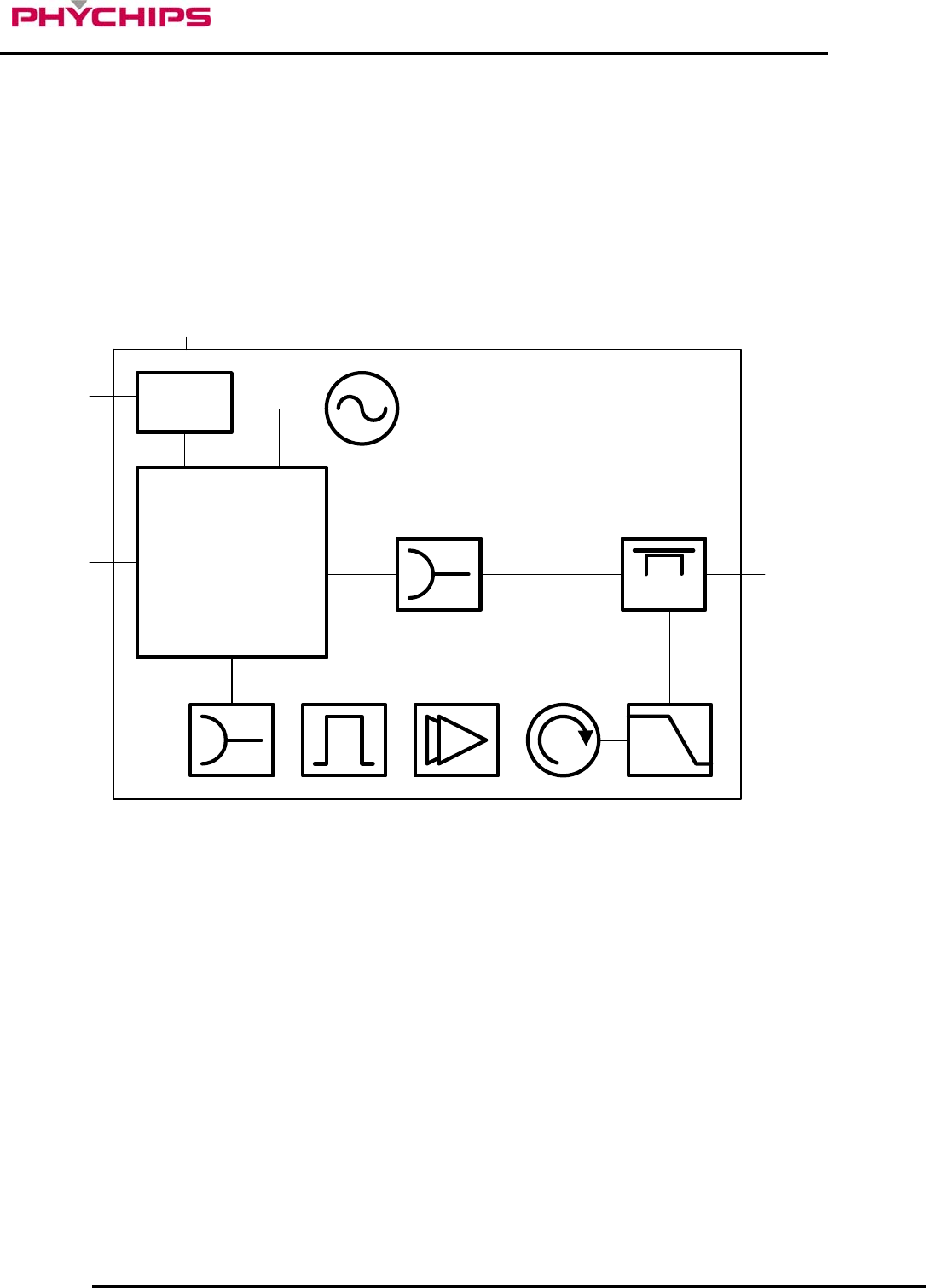
1 Overview & Block Composition Diagram
1.1 Overview
The PRM90U10A is a UHF RFID Reader hybrid module which integrates high performance UHF RFID reader
chipset, VC-TCXO, Low Drop Regulator, Balun, Coupler, Saw filter, Power amp, Isolator and low pass filter.
UHF RFID reader chipset uses PR9000 of PHYCHIPS which integrates 900MHz radio, baseband processor,
industry standard enhanced 8052 MCU, memory (64k Flash & 16k SRAM) and many other features.
This module fully compliant with ISO18000-6C/EPC Global Gen II reader protocol and provide all functions of
PR9000. Also reduce size, cost and power consumption.
1.2 Block Domposition Diagram
PR9000
LDO
BALUN
DC 3.6V/500mA
GPIO
SHDNb
RF I/O
BALUN SAW
AMP
LPF
COUPLER
PRM90K10x
19.2MHz TCXO
Figure 1 Block Composition Diagram
9 December 2010 4 of 13
PRM90U10A Specification- Preliminary Version
2 Pin Description
7
8
1
2
3
4
5
6
9
10
11
12
13
14
15
16
17
18
19
20
21
22
23
24
25
26
27
28
29
30
7
8
1
2
3
4
5
6
9
10
11
12
13
14
15
16
17
18
19
20
21
22
23
24
25
26
27
28
29
30
12345678910111213141516
35 34 33 3231 30 2928 2726 25 24 2322 21 20
17
18
19
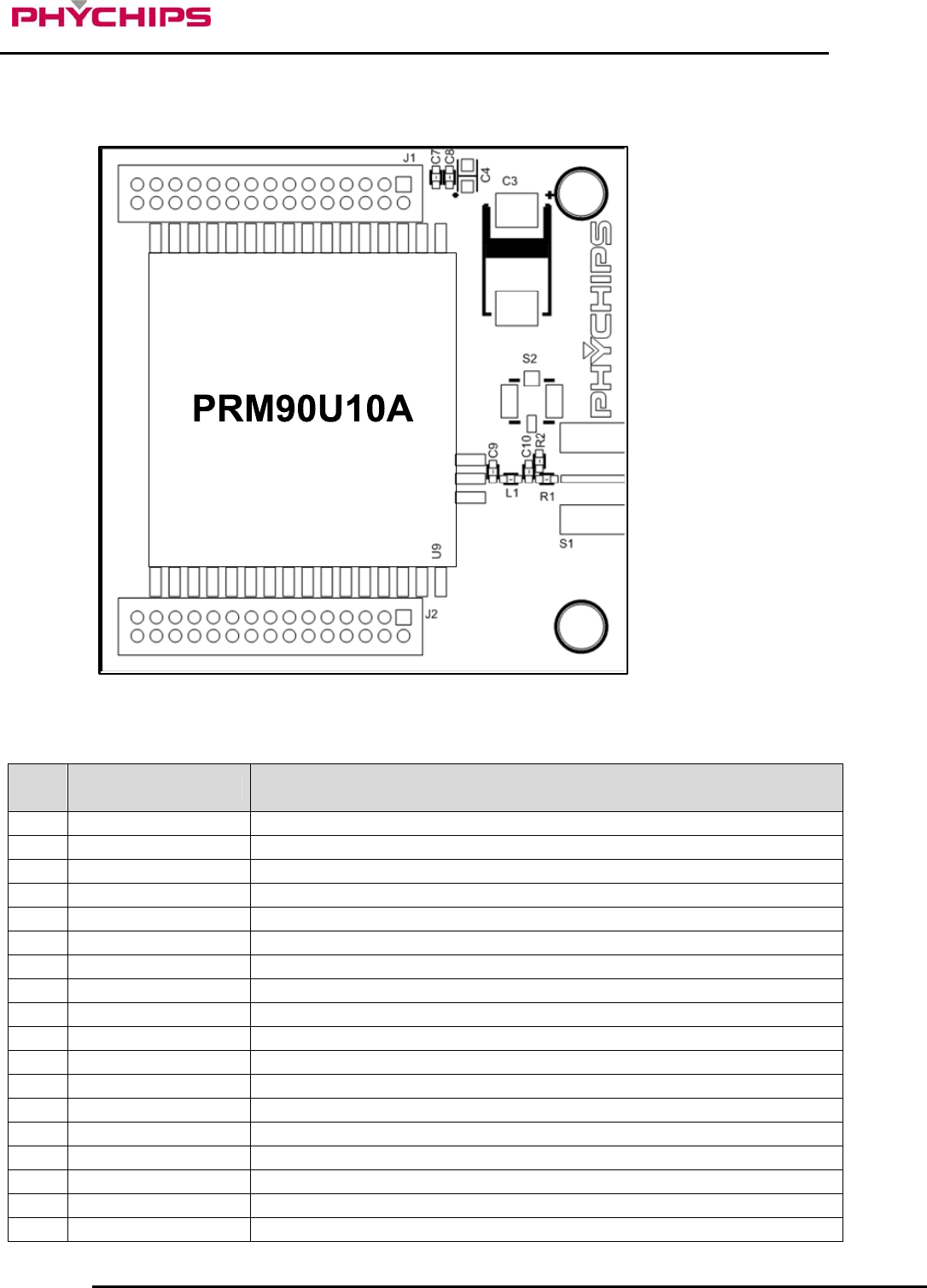
Figure 2 Pin Description
2.1 J1 Pin Description
No. Pin Name Description
1 VDD_3.6V 3.6 V DC Power for SOC(Max. 1A)
2 VDD_3.6V 3.6 V DC Power for SOC(Max. 1A)
3 VDD_3.6V 3.6 V DC Power for SOC(Max. 1A)
4 VDD_3.6V 3.6 V DC Power for SOC(Max. 1A)
5 GND Ground
6 GND Ground
7 GND Ground
8 GND Ground
9 NC Reserved, Not Ground
10 NC Reserved, Not Ground
11 NC Reserved, Not Ground
12 NC Reserved, Not Ground
13 GND Ground
14 GND Ground
15 NC Reserved, Not Ground
16 NC Reserved, Not Ground
17 GND Ground
18 GND Ground
9 December 2010 5 of 13
PRM90U10A Specification- Preliminary Version
19 P2.2 Quasi-bidirectional I/O port
20 NC Reserved, Not Ground
21 MDS_SCL I/O for ISP. The pull-up resistor is always switched on. This port is quasi-
bidirectional
22 MDS_SDA I/O for ISP. The pull-up resistor is always switched on. This port is quasi-
bidirectional
23 GND Ground
24 RESETb External Reset for SOC
25 P0.1 Quasi-bidirectional I/O port or Serial Port 0 Output
26 P0.0 Quasi-bidirectional I/O port or Serial Port 0 Input
27 NC Reserved, Not Ground
28 P0.2 Quasi-bidirectional I/O port or External Interrupt Input 0
29 P0.5 Quasi-bidirectional I/O port or Timer 1 External Input or SPI Master Output
Slave Input
30 P0.4 Quasi-bidirectional I/O port or Timer 0 External Input or SPI Master Input
Slave Output
2.2 J2 Pin Description
No. Pin Name Description
1 NC Reserved, Not Ground
2 NC Reserved, Not Ground
3 GND Ground
4 GND Ground
5 NC Reserved, Not Ground
6 NC Reserved, Not Ground
7 GND Ground
8 GND Ground
9 TXD1 Quasi-bidirectional I/O port or Serial Port 1 Output
10 RXD1 Quasi-bidirectional I/O port or Serial Port 1 Input
11 GND Ground
12 GND Ground
13 P1.7 Quasi-bidirectional I/O port or External Interrupt 5 (Negative Edge)
14 P1.6 Quasi-bidirectional I/O port or External Interrupt 4 (Positive Edge)
15 P1.5 Quasi-bidirectional I/O port or External Interrupt 3 (Negative Edge)
16 P1.4 Quasi-bidirectional I/O port or External Interrupt 2 (Positive Edge)
17 P1.3 Quasi-bidirectional I/O port or I2C SCL
18 P1.2 Quasi-bidirectional I/O port or I2C SDA
19 P1.1 Quasi-bidirectional I/O port or Timer/ Counter 2 Capture/Reload Trigger
20 P1.0 Quasi-bidirectional I/O port or External Input for Timer/Counter 2
21 P0.7 Quasi-bidirectional I/O port or SPI Slave Select Bar
22 P0.6 Quasi-bidirectional I/O port or SPI SCK
23 NC Reserved, Not Ground
24 NC Reserved, Not Ground
25 NC Reserved, Not Ground
26 NC Reserved, Not Ground
27 GND Ground
28 GND Ground
29 SHDNb
Module Enable/Disable
Enable : Open
Disable : Ground
9 December 2010 6 of 13
PRM90U10A Specification- Preliminary Version
30 SHDNb
Module Enable/Disable
Enable : Open
Disable : Ground
2.3 S1 Pin Description(RF I/O)
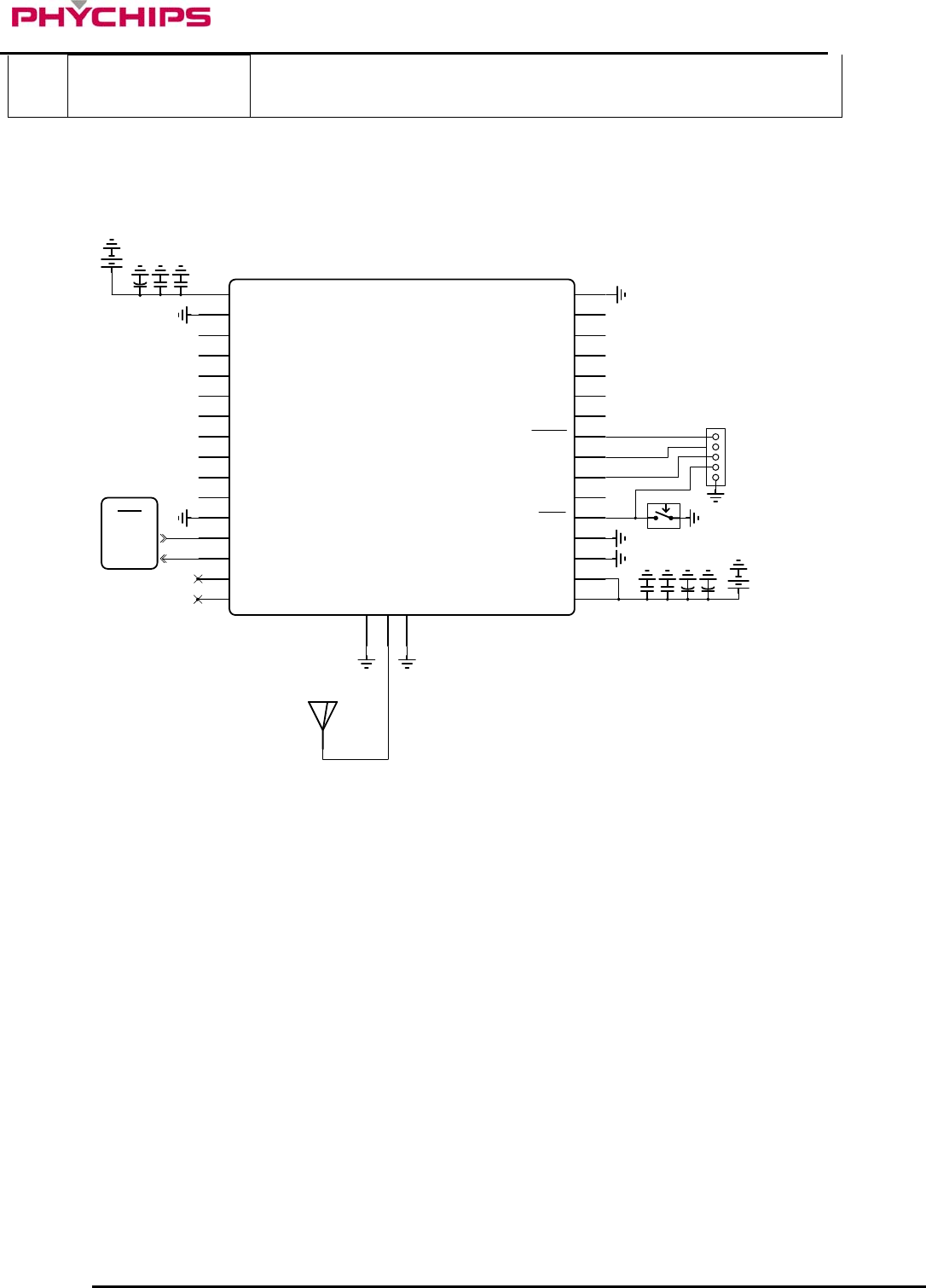
3 Operation method
DC 3.6V
/150mA
DC 3.6V
/350mA
NC NC
ANT
1nF
0.1uF10uF
1nF 0.1uF10uF100uF
ISP
RESET
MDS_SDA
MDS_SCK
VDD
GND
OPEN : NORMAL
CLOSE : SHUT DOWN
UART
TXD
RXD
PRM90U10A
VDD_36
GND
NC
TXD1
RXD1
GND
P1.7
P1.6
P1.5
P1.4
P1.3
P1.2
P1.1
P1.0
P0.7
P0.6
P0.5
GND
RFIO
GND
NC
GND
P0.4
VDDPA_36
VDDPA_36
GND
GND
SHDN
P2.2
MDS_SCL
MDS_SDA
RESET
P0.0
P0.1
P0.2
1
2
3
4
5
6
7
8
9
10
11
12
13
14
15
16
17
18
19
20
21
22
23
24
25
26
27
28
29
30
31
32
33
34
35
Figure 3 Application Circuit
3.1 Power Supply
PRM90U10A should be supplied by 2 kinds of 3.6 volts DC power; VDD_36(Pin 1) and VDDPA_36(Pin 20,
21). VDD_36 is for operating of PR9000 RFID reader chipset which current consumption is about 150mA.
VDDPA_36 is for operating of power amp which current consumption is 350mA typically.
Additionally, decoupling capacitors should be placed as close as possible these pins. The decoupling
capacitors should be placed in the same layer as the module, to avoid any additional parasitic inductance
caused by vias.
3.2 Hardware Mode Control
PRM90U10A provides normal mode and shut down mode. The mode can control by SHDNb(Pin 24).
Normal mode should be controlled by SHDN pin to open which can activate the module. Otherwise, If SHDNb
pin contact to ground, supplied power of the module is shut down internally. In shut down mode, all GPIO
ports and UART ports should not input any signal and positive voltage.
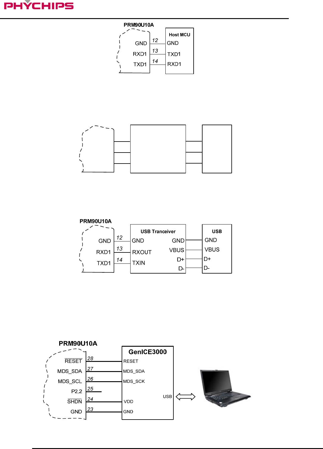
3.3 UART
The serial interface assigned to two pins. RXD1(Pin 13) is for receiving command from host and TXD1(Pin 14)
is for transmitting response to host. Pin connection is shown as below figure.
9 December 2010 7 of 13
PRM90U10A Specification- Preliminary Version
Figure 4 Connecting to host MCU
RS232C transceiver is required for interfacing to PC and diagram connection is shown as below figure.
RS232C Tranceiver
TXD1
RXD1
GND 12
13
14
RXOUT
TXIN
GND
TXOUT
RXIN
GND
PC
TXD
RXD
GND
PRM90U10A
Figure 5 Connecting to RS232 transceiver
Following configuration is used for interfacing to USB transceiver.
Figure 6 Connecting to USB transceiver
3.4 ISP
For firmware downloading in PRM90U10A should be used GenICE3000 by CORERIVER(manufacturer),
which downloading speed is faster than UART. Code memory(62kB) and EEPROM(2kB) can be programmed
using EJTAG in target.
Following configuration is used for downloading to GenICE3000.
Figure 7 Connecting to GenICE3000 for firmware downloading
9 December 2010 8 of 13
PRM90U10A Specification- Preliminary Version
3.5 GPIO
PRM90U10A provides 16 bi-directional I/O ports. All ports can be configured in two different modes: open-
drain (by default) and push-pull which has 3.3V input and 3.3V output.
3.6 RF In/Out
RF I/O(Pin 20) is optimized at 50 ohms impedance.
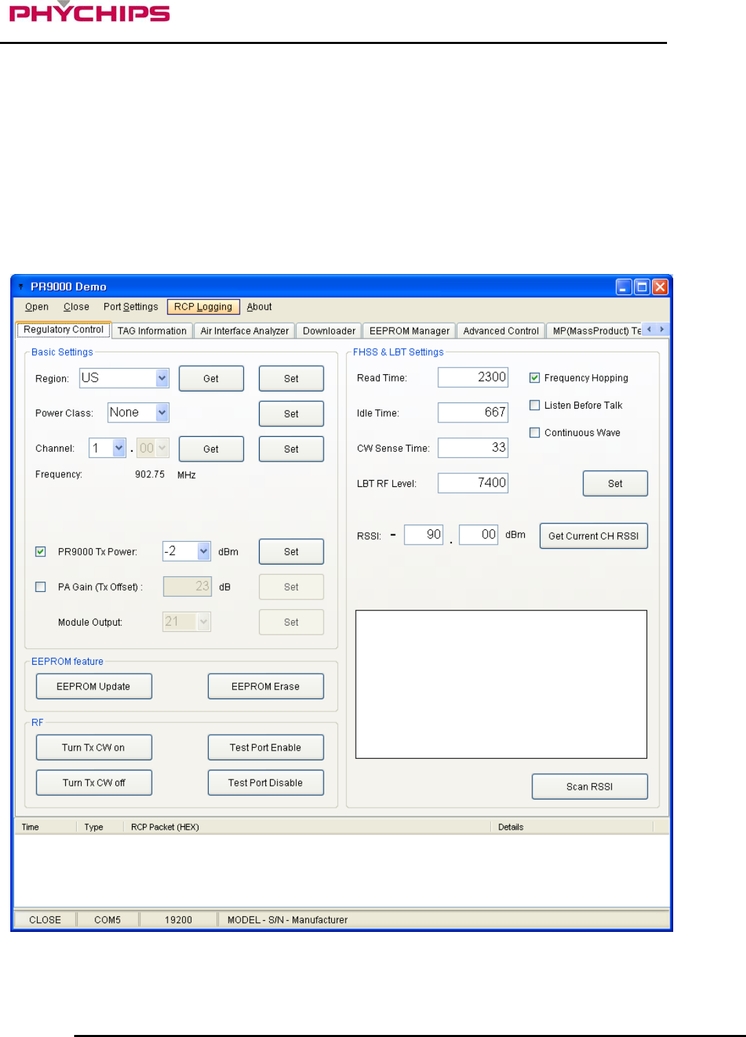
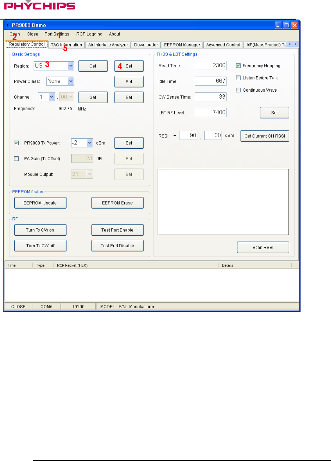
3.7 Using GUI
The GUI is for the user to be able to quickly get started working with PRM90U10A RFID reader. To run the
GUI, click the Windows start button, Program menu, Phychips, PR9000 SDK. After start-up, a window will be
opened as shown below.
Figure 8 Demo GUI
9 December 2010 9 of 13
PRM90U10A Specification- Preliminary Version
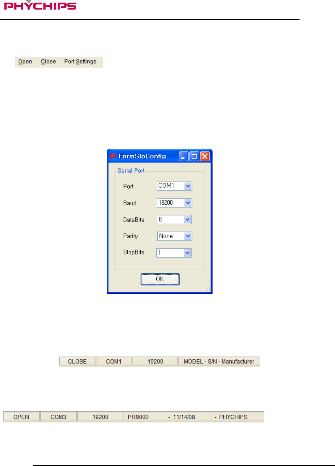
3.7.1 Serial Port Control
Serial port is controlled by below menu.
To open serial port, click Open menu.
To close serial port, click Close menu.
3.7.1.1 Serial Port Configurations
Port number is selectable from COM1 upto COM9. (Depending on your Windows system settings) Baud Rate
should be set 19200 bps.
Figure 9 Serial Port Settings
3.7.1.2 Reader Connection Status
Below status bar shows the reader connection status.
Figure 10 Reader Connection Statuses
If PC is successively connected to reader after clicking open button, status bar would be updated as shown
below.
9 December 2010 10 of 13
PRM90U10A Specification- Preliminary Version
3.7.2 Hardware Control
To control hardware, click ‘H/W Control Tab.’
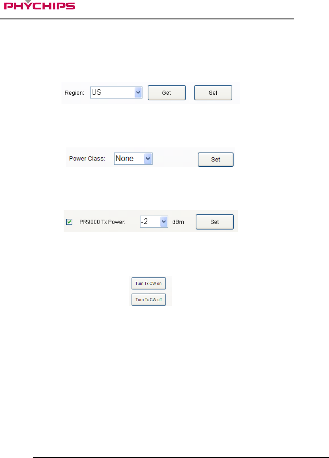
3.7.2.1 Band setting
To select operating band, band setting should be required. Select band in combo box and click Set button to
set operating band in group box ‘Basic settings.’
3.7.2.2 Power Class setting
Some countries classified channel numbers according to the power class. Select the power class and click Set
button.
.
3.7.2.3 Output Power setting
To set PR9000 output power, select the PR9000 Tx Power combo box and click Set button.
3.7.2.4 CW (Continuous Wave) setting
These buttons are used for hardware debugging purpose only. To turn CW on, click Turn Tx CW on button. To
turn CW off, click Turn Tx CW off button.
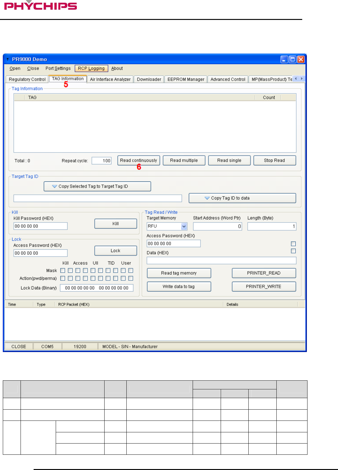
3.7.3 Procedures for Tags Inventory Operation
To read UHF RFID tags with PR9000 SDK software, follow sequence as described below.
Configure your serial port settings.
Open serial port. Then, PR9000 SDK software will try connecting to PR9000.
Select operation band and click ‘Set’ button.
Click ‘Tag Information’ tab.
9 December 2010 11 of 13
PRM90U10A Specification- Preliminary Version
Figure 11 Procedures for tag inventory operation
9 December 2010 12 of 13
PRM90U10A Specification- Preliminary Version
Click ‘Read multiple’ button to start reading RFID tags.
Figure 12 Procedures for tag inventory operation
4 Specification Specification
No. Item Unit Test Condition min Typ. max Remark
1 Freq. Range MHz 902.75 927.25
2 Tx Power dBm PR9000 = 4dBm 25.5
+/-200kHz dBc PR9000 = 4dBm -20
+/-400kHz dBc PR9000 = 4dBm -50
3 Tx ACPR
+/-600kHz dBc PR9000 = 4dBm -60
9 December 2010 13 of 13
PRM90U10A Specification- Preliminary Version
+/-800kHz dBc PR9000 = 4dBm -65
GPIO = HIGH - GPIO = ALL HIGH HIGH
4 GPIO GPIO = LOW - GPIO = ALL LOW LOW
5 Impedance Ω 50 RF I/O
6 DC Power V 3.6
7 OperatingTemperature °C 0 50
8 Operating Humidity % 0 60
SHDN 2
IDLE 16
9 Consumption
Current
ACTIVE
mA
PR9000 = 4dBm 500 550
10 Modulation - DSB - ASK
11 Size mm 35x45x8
12 Weight g 11
Cautions
Modifications not expressly approved by the party responsible for compliance could void the user’s authority to
operate the equipment.
FCC Information to User
This equipment has been tested and found to comply with the limits for a Class B digital device, pursuant to
Part 15 of the FCC Rules. These limits are designed to provide reasonable protection against harmful
interference in a residential installation. This equipment generates, uses and can radiate radio frequency
energy and, if not installed and used in accordance with the instructions, may cause harmful interference to
radio communications. However, there is no guarantee that interference will not occur in a particular
installation. If this equipment does cause harmful interference to radio or television reception, which can be
determined by turning the equipment off and on, the user is encouraged to try to correct the interference by
one of the following measures:
• Reorient or relocate the receiving antenna.
• Increase the separation between the equipment and receiver.
• Connect the equipment into an outlet on a circuit different from that to which the receiver is con-nected.
• Consult the dealer or an experienced radio/TV technician for help.
FCC Compliance Information : This device complies with Part 15 of the FCC Rules. Operation
is subject to the following two conditions: (1) This device may not cause harmful interference, and (2) this
device must accept any interference received, including interference that may cause undesired operation
FCC WARNING:
This equipment may generate or use radio frequency energy. Changes or modifications to this equipment
may cause harmful interference unless the modifications are expressly approved in the instruction manual.
The user could lose the authority to operate this equipment if an unauthorized change or modification is made.
FCC RF EXPOSURE:
The EUT will only be used with a separation of 20 centimeters or greater between the antenna and the body
of the user.