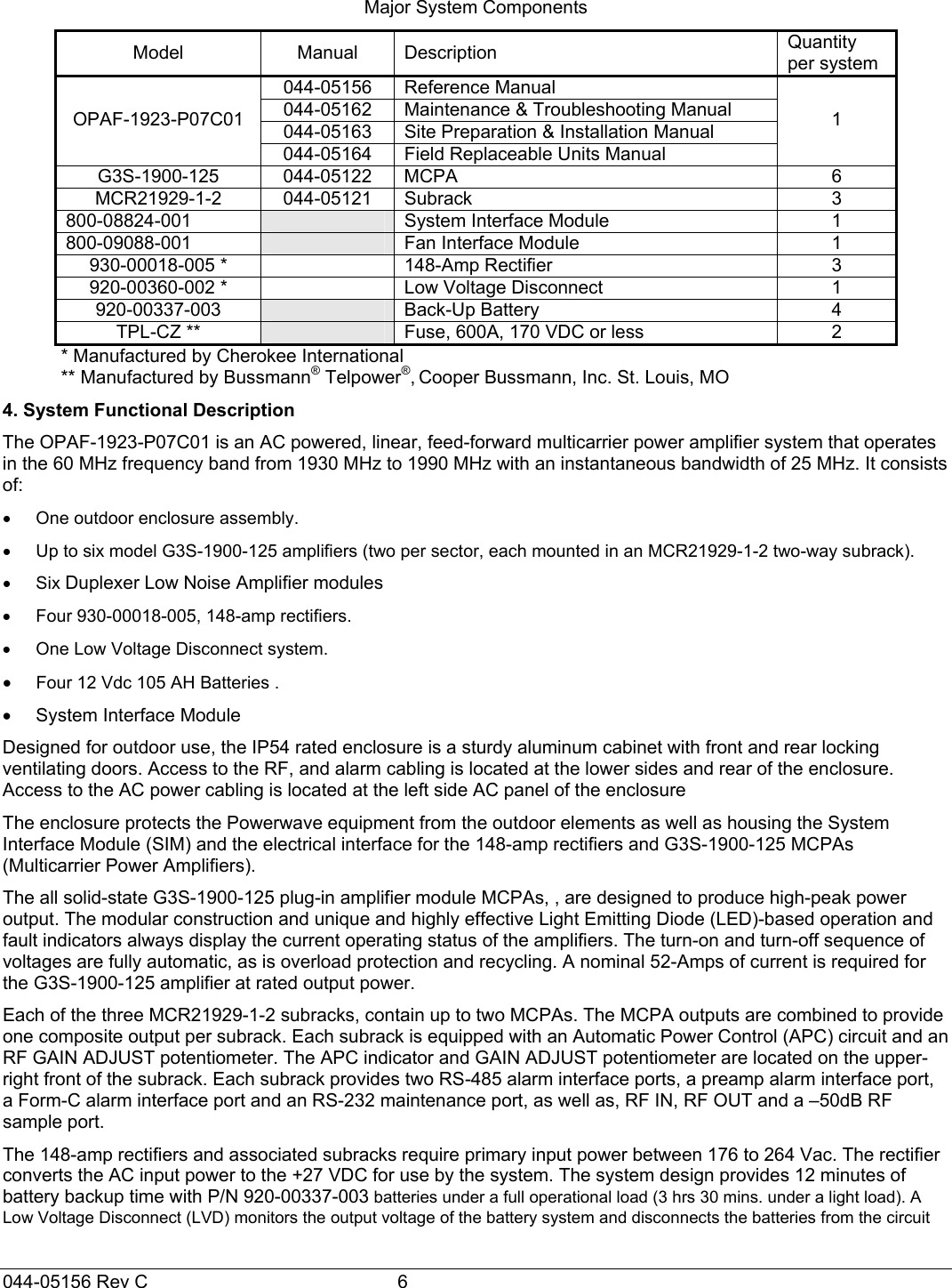
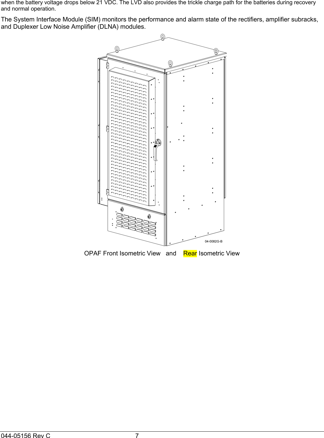
Powerwave Technologies 5JS0070 Three Sector 1900 MHz RF Power Amplifier Cabinet User Manual
Powerwave Technologies Inc Three Sector 1900 MHz RF Power Amplifier Cabinet Users Manual
UserManual.wiki
>
Powerwave Technologies
>
5JS0070 User Manual
Users Manual
Navigation menu
Upload a User Manual
Namespaces
Wiki Guide
HTML
PDF
Info
Views
User Manual
Discussion / Help
Navigation
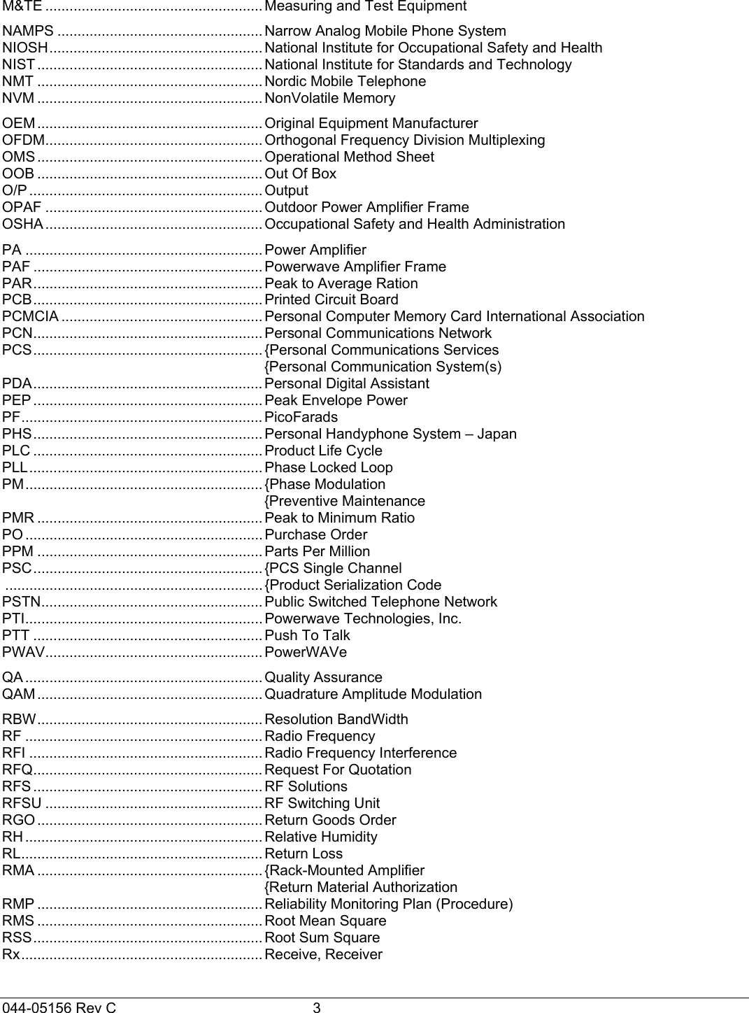
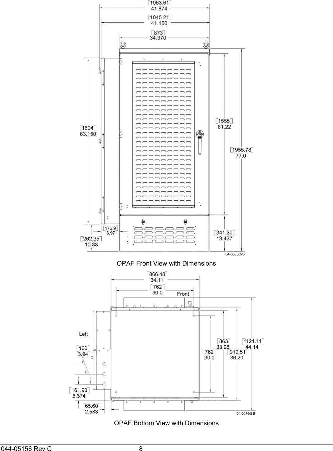
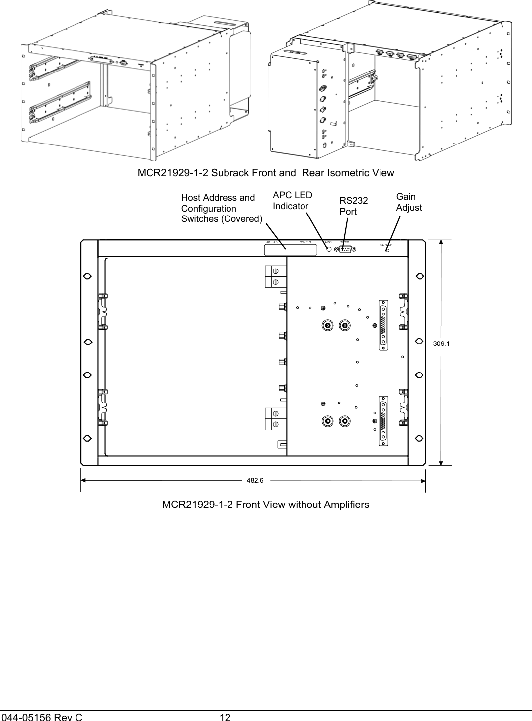
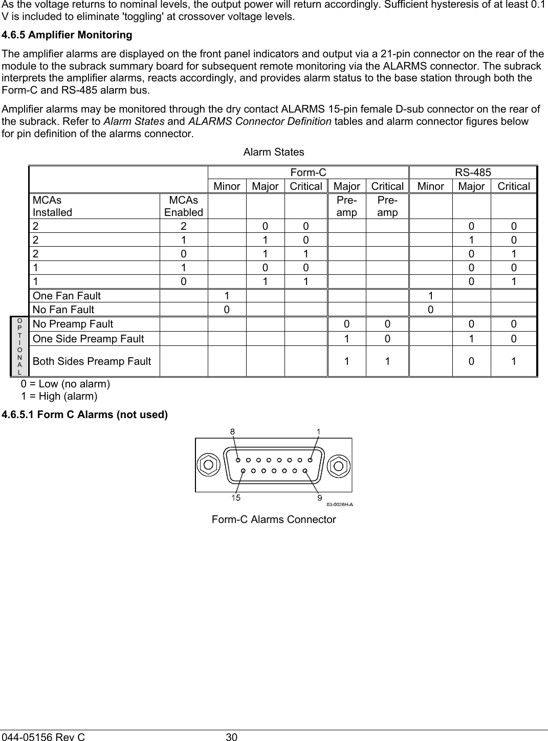
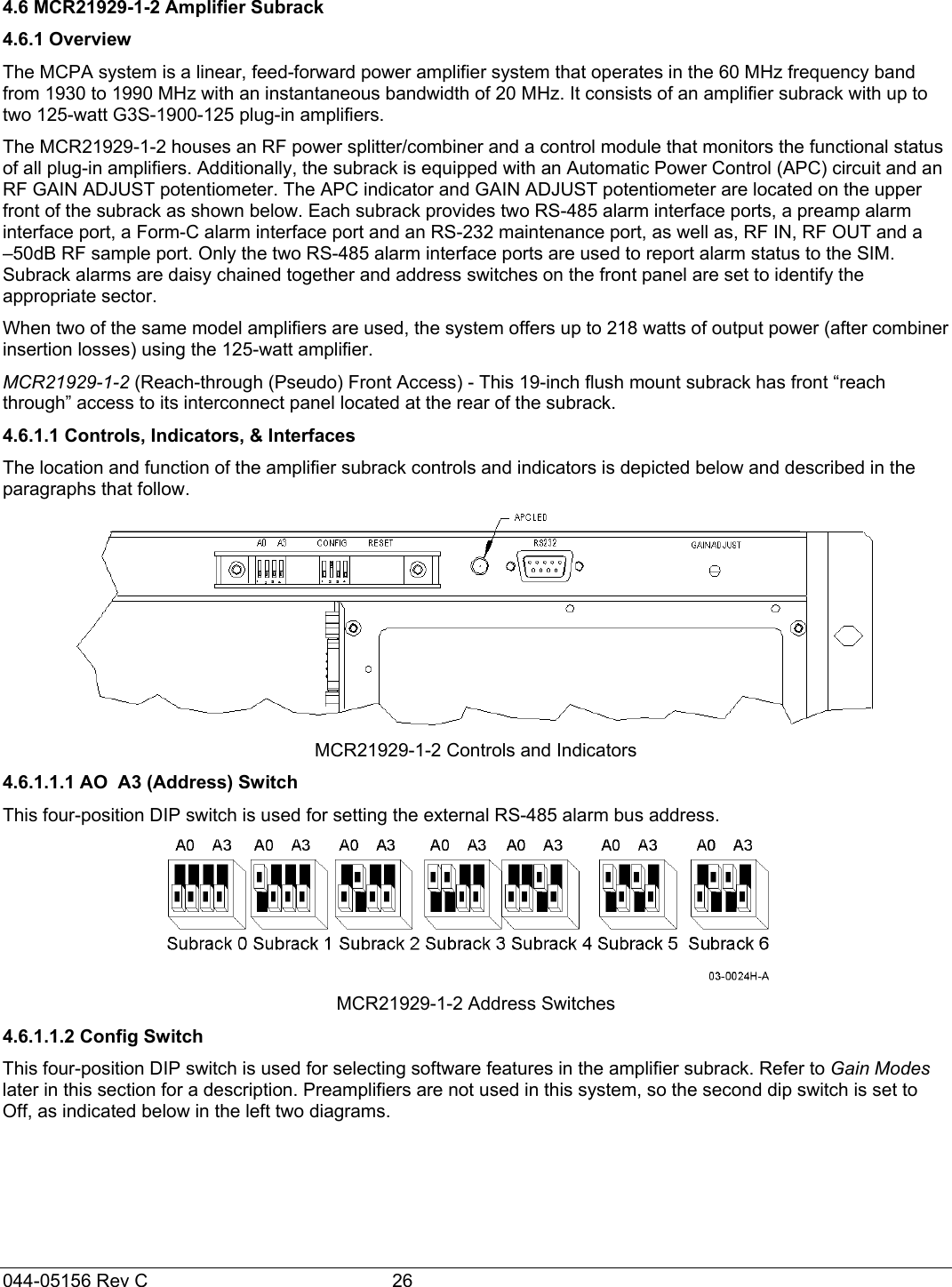
![044-05156 Rev C 24 Although each amplifier module contains its own heat sink, it is cooled with forced air. Four fans are used for forced air cooling and redundancy. The fans, located on the front and rear of the amplifier module, draw air in through the front of the amplifier and exhaust hot air out the back of the module. The fans are field replaceable. 4.5.3 Intermodulation The G3S-1900-125 amplifier is designed to deliver a 125-watt composite average power, multicarrier signal, occupying a bandwidth less than or equal to 20 MHz, in the bandwidth from 1930 to 1990 MHz. The maximum average power for linear operation, and thus the amplifier efficiency, will depend on the type of signal amplified. 4.5.3.1 Two Tone Intermodulation When measured with two equal CW tones spaced anywhere from 30 kHz to 20 MHz apart, and at any power level up to the average power, the third order intermodulation products will be below -63 dBc 4.5.3.2 Multitone Intermodulation Adding more tones to the signal will lower individual intermodulation products. If the frequencies are not equally spaced, the level of intermodulation products gets very low. When the frequencies are equally spaced, those products fall on top of each other on the same frequency grid. The average power of all intermodulation beats falling on the same frequency is called the composite intermodulation; it is -63 dBc or better. 4.5.4 Amplifier Monitoring The amplifier has a separate remote alarm and control connector, which may be used by the host system to monitor and control the individual amplifier modules. The status, alarm, control, and power connections on the amplifier connector are made through a 21-pin male D-Sub combo connector and are listed and described in the Amplifier Module DC and Logic Connector Definition table. A1 A2 A3 A41 2 3 4 5 6 7 8 910 11 12 13 14 15 16 17 DC and Logic Connector (Male, on Rear of G3S-1900-125 Amplifier Module] Amplifier Module DC and Logic Connector Definition PIN Function Description A1 Power Input +27 Vdc (Power Contact) A2 Power Input +27 Vdc (Power Contact) A3 Ground Ground (Power Contact) A4 Ground Ground (Power Contact) 1 RS485 +TxD Serial Communication Data Out 2 RS485 +RxD Serial Communication Data In 3 Service Loop TTL input to Amp. Gnd. for special test mode (Note 1) 4 MCPA Disabled (Summary Fault) TTL signal normally low indicates MCPA enabled. A high level indicates that the MCPA has been disabled. Over Power, Over Voltage takes one second to activate the signal. 5 Mod Addr 0 TTL input to Amp. Gnd. supplied by shelf to identify slot. 6 Mod Addr 1 TTL input to Amp. Gnd. supplied by shelf to identify slot. 7 TP1 TTL output. Future test point. 8 Manual Download GND to download manually 9 DC on stat TTL output. High indicates Amp is powered on. 10 RS485 –TxD Serial Communication Data Out 11 RS485 –RxD Serial Communication Data In 12 SCL7 No connection 13 SDA7 No connection 14 FP Disable Output Output, GND if the front panel switch is in the OFF position; +5 volts indicates the front panel switch is in the ON position. 15 FP RST Output, GND if the front panel switch is in the RESET position; +5 volts otherwise. 16 GND Ground 17 Module Detect Ground potential. Informs the subrack that an MCPA is plugged in.](https://usermanual.wiki/Powerwave-Technologies/5JS0070/User-Guide-470503-Page-24.png)
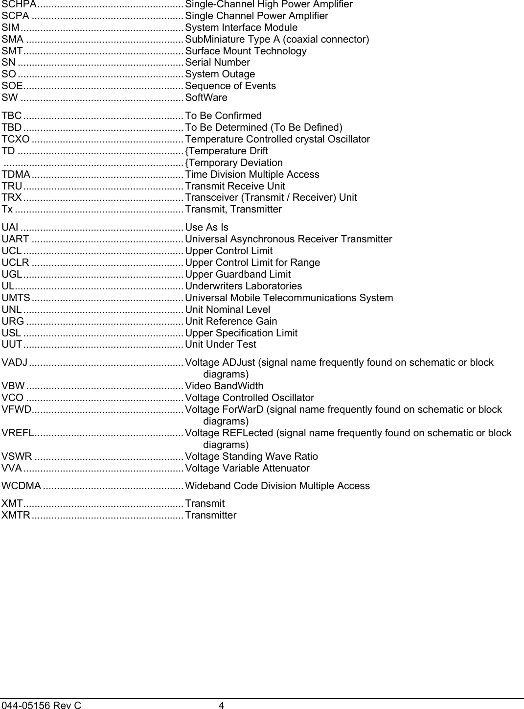
![044-05156 Rev C 29 4.6.3.1 Standard Gain Overview and Application (Default Configuration) In the standard gain mode, the gain of the system is dependent on the number of amplifiers operating at a given time and the power from the amplifiers is used at or near their maximum limits. When the design of the cell site requires full power from the amplifiers installed in the subrack in order to achieve maximum call capacity, the standard gain mode should be used. For example, if the sector design calls for 150 watts (measured at the directional coupler output; assuming 1.5 dB of loss from the subrack to the directional coupler), the sector should be configured with two 125 watt amplifiers (154 watts at directional coupler; 51.5 dB subrack system gain) to take full advantage of the available power. The trade-off here, is that if an amplifier fails, the available power drops back to 77 watts, the overall gain drops by 3.0 dB, and all the transmit channel powers drop by 3.0 dB as well (i.e. 7.5 watts to 3.75 watts per channel). Gain adjustment via the front panel potentiometer is available. 4.6.3.2 Constant Gain Overview and Application In constant gain mode, the gain of the subrack remains the same, regardless of the number of amplifiers installed. Good engineering practice requires careful planning when using constant gain mode. When the design of the cell site requires much less than maximum power, but must maintain a specific radius of coverage, constant gain mode is ideal. For example, if the sector design calls for 75 watts output power at the directional coupler, the sector must be configured with two 125 watt amplifiers (87 watts; 48 dB gain) when constant gain is enabled to allow for amplifier failure. If an amplifier fails, the available power drops back to 43 watts, the subrack gain adjusts to remain 48 dB (77 watts), and all the transmit channel powers remain at the set power (i.e. 7.5 watts per channel). However, while in constant gain mode, if the sector power is set to maximum (i.e. 100 watts with two amplifiers installed), and an amplifier fails, the remaining amplifier will be over-driven and likely to go into an over power condition. Should this occur, the sector would go into APC control, the input power is attenuated (see paragraph 4-5), the sector’s footprint shrinks and an alarm is sent to the switch. Gain adjustment via the front panel potentiometer is available. 4.6.3.3 Gain Mode Control and Theory The MCR21929-1-2 subrack adds 3 dB of attenuation when constant gain mode is initially activated, reducing the system gain of the MCR21929-1-2 from a nominal of 51.5 dB to 48.5 dB. Therefore, whenever the gain mode is changed from standard gain to constant gain or visa-versa, the cell technician must reset the overall system gain or individual channel power. In constant gain mode, the gain of each carrier (or the system) must remain constant to avoid reducing the cell radius. When the subrack detects an amplifier failure, the amplifier subrack reduces input attenuation through the Voltage Variable Attenuator (VVA) by the amount of gain lost while the amplifier is removed from the circuit. This allows the system gain to remain constant, and allows the cell site to maintain a consistent footprint. When the replaced MCPA is enabled, attenuation is again added to the input port of the subrack by the amount of gain introduced by the replacement MCPA to maintain an overall subrack constant gain. As MCPAs are disabled and enabled, system gain is recovered within a 1-second time frame. The subrack is shipped from the factory with the configuration switch set for Standard Gain mode active. 4.6.4 Performance Derating With Lower Supply Voltage The MCPA system will operate at full power, while meeting all spectrum requirements, over a supply voltage range of 26 to 28 VDC. The MCPA System will meet derated spectrum requirements at derated output power levels over a supply voltage range of 21 to 30 VDC. MCPA System power derating levels are outlined in below. The LED indicator located on the top front right of the subrack blinks when the output power is derated. Power Derating Versus Voltage Profile Supply Voltage[VDC] Output Power Derating 28V ≤ V < 30V 0.5dB 26V ≤ V < 28V 0dB 24V ≤ V < 26V 0.5dB 22V ≤ V < 24V 1.0dB 21V ≤ V < 22V 1.5dB](https://usermanual.wiki/Powerwave-Technologies/5JS0070/User-Guide-470503-Page-29.png)