Powerwave Technologies 5JS0070 Three Sector 1900 MHz RF Power Amplifier Cabinet User Manual
Powerwave Technologies Inc Three Sector 1900 MHz RF Power Amplifier Cabinet Users Manual
Users Manual

044-05156 Rev C 1
Reference Manual
1. Abbreviations and Acronyms
Abbreviation / Acronym Definition
{ = Two definitions,
{ same abbreviation/acronym
ACLR....................................................... Adjacent Channel Leakage Power Ratio
ACP......................................................... Adjacent Channel Power
A/D .......................................................... Analog-to-Digital Conversion
ADC......................................................... {Analog-to-Digital Converter
{Automatic Data Collection
AM........................................................... Amplitude Modulation
AMPS ...................................................... Advanced Mobile Phone System
ANSI........................................................ American National Standards Institute
APC......................................................... Automatic Power Control
APTT ....................................................... Analog Push To Talk
ASG......................................................... Applications Support Group
ASIC........................................................ Application Specific Integrated Circuit
ATE ......................................................... Automatic (Automated) Test Equipment
ATP ......................................................... Acceptance Test Procedure
ATTEN .................................................... Attenuator
BER......................................................... Beyond Economical Repair
BOM ........................................................ Bill Of Materials
BPF ......................................................... Band Pass Filter
BS ...........................................................Base Station
BTS ......................................................... Base Transceiver Station (System)
BW .......................................................... BandWidth
°C ............................................................ Degrees Celsius
CAD......................................................... Computer Aided Design
CCA......................................................... {Circuit Card Assembly
CCW........................................................ Counter ClockWise
CDMA...................................................... Code Division Multiple Access
CDPD ...................................................... Cellular Digital Packet Data
CTRL....................................................... Control
CW .......................................................... {ClockWise
{Continuous Wave
dB............................................................ deciBels
dBc .......................................................... Referenced to a carrier level
dBm......................................................... Reference to a specific power level (one milliwatt)
dBw ......................................................... Reference to a specific power level (one watt)
DIN ......................................................... Deutsches Insitut für Normung eV
DLNA....................................................... Duplexer Low Noise Amplifier
DPTT....................................................... Digital Push To Talk
DQPSK.................................................... Differential Quadrature Phase Shift Keyed
DSP......................................................... Digital Signal Processing
DUT......................................................... Device Under Test
ECD......................................................... Estimated Completion Date
ECM ........................................................ Electronic Counter Measure
EDGE ...................................................... Enhanced Data for GSM Evolution
EEPROM................................................. Electrically-Erasable Programmable Read-Only Memory
EIA ..........................................................Electronic Industries Association
EMC ........................................................ ElectroMagnetic Compatibility
EMI.......................................................... ElectroMagnetic Interference
EPROM ................................................... {Electrically Programmable Read-Only Memory
{Erasable Programmable Read-Only Memory

044-05156 Rev C 2
ESD......................................................... ElectroStatic Discharge
ESG......................................................... Electronic Signal Generator
ETDMA.................................................... Extended Time Division Multiple Access
ETSI ........................................................ European Telecommunications Standard Institute
EUT ......................................................... Equipment Under Test
FAR ......................................................... Failure Analysis Report
FCC......................................................... Federal Communications Commission
FDMA ...................................................... Frequency Division Multiple Access
FET ......................................................... Field Effect Transistor
FHMA ...................................................... Frequency Hopping Multiple Access
FM ........................................................... Frequency Modulation
FRU......................................................... Field Replaceable Unit
FSK ......................................................... Frequency Shift Key modulation
GHz ......................................................... GigaHertz
GMSK...................................................... Gaussian Minimum Shift Keying
GOLAY.................................................... See GSC
GSC ........................................................ Golay Sequential Code
GSM ........................................................ Global System for Mobile Communications
HPF ......................................................... High Pass Filter
HW .......................................................... Hardware
Hz............................................................ Hertz
IAW ......................................................... In Accordance With
IC............................................................. Integrated Circuit
IMD.......................................................... InterModulation Distortion
IRL........................................................... Input Return Loss
IS-54........................................................ Interim Standard 54 for TDMA
IS-95........................................................ Interim Standard 95 for CDMA
ISDN........................................................ Integrated Services Digital Network
ISM.......................................................... Industrial, Scientific and Medical unlicensed frequency bands
ISO .......................................................... {International Organization for Standardization
{ISOlator
kHz .......................................................... KiloHertz
LDA ......................................................... Linear Discrete Amplifier (Class A or AB)
LGL ......................................................... Lower Guardband Limit
LMR......................................................... Land Mobile Radio
LMS......................................................... Land Mobile Systems
LNA ......................................................... Low Noise Amplifier
LO ........................................................... Local Oscillator
LPA ......................................................... Linear Power Amplifier
LPF.......................................................... Low Pass Filter
LSL.......................................................... Lower Specification Limit
LVD ......................................................... Low Voltage Disconnect
MC........................................................... MultiChannel
MCA ........................................................ MultiChannel Amplifier
MCPA...................................................... {MultiCarrier Power Amplifier
{MultiChannel Power Amplifier
MCR ........................................................ MultiChannel Rack
MFRM ..................................................... {Multiple Frequency Radio Mobile
{Multifunction Frequency Radio Modulation
MHz......................................................... MegaHertz
MSO ........................................................ Master Switch Office
MTBF ...................................................... Mean Time Between Failures
MTSO...................................................... Master Telephone Switch Office
MU........................................................... Measurement Uncertainty

044-05156 Rev C 3
M&TE ...................................................... Measuring and Test Equipment
NAMPS ................................................... Narrow Analog Mobile Phone System
NIOSH..................................................... National Institute for Occupational Safety and Health
NIST ........................................................ National Institute for Standards and Technology
NMT ........................................................ Nordic Mobile Telephone
NVM ........................................................ NonVolatile Memory
OEM ........................................................ Original Equipment Manufacturer
OFDM...................................................... Orthogonal Frequency Division Multiplexing
OMS ........................................................ Operational Method Sheet
OOB ........................................................ Out Of Box
O/P .......................................................... Output
OPAF ...................................................... Outdoor Power Amplifier Frame
OSHA ...................................................... Occupational Safety and Health Administration
PA ...........................................................Power Amplifier
PAF ......................................................... Powerwave Amplifier Frame
PAR......................................................... Peak to Average Ration
PCB......................................................... Printed Circuit Board
PCMCIA .................................................. Personal Computer Memory Card International Association
PCN......................................................... Personal Communications Network
PCS......................................................... {Personal Communications Services
{Personal Communication System(s)
PDA......................................................... Personal Digital Assistant
PEP ......................................................... Peak Envelope Power
PF............................................................ PicoFarads
PHS......................................................... Personal Handyphone System – Japan
PLC ......................................................... Product Life Cycle
PLL.......................................................... Phase Locked Loop
PM........................................................... {Phase Modulation
{Preventive Maintenance
PMR ........................................................ Peak to Minimum Ratio
PO ........................................................... Purchase Order
PPM ........................................................ Parts Per Million
PSC......................................................... {PCS Single Channel
................................................................ {Product Serialization Code
PSTN....................................................... Public Switched Telephone Network
PTI........................................................... Powerwave Technologies, Inc.
PTT ......................................................... Push To Talk
PWAV...................................................... PowerWAVe
QA ........................................................... Quality Assurance
QAM ........................................................ Quadrature Amplitude Modulation
RBW........................................................ Resolution BandWidth
RF ........................................................... Radio Frequency
RFI .......................................................... Radio Frequency Interference
RFQ......................................................... Request For Quotation
RFS ......................................................... RF Solutions
RFSU ...................................................... RF Switching Unit
RGO ........................................................ Return Goods Order
RH ........................................................... Relative Humidity
RL............................................................ Return Loss
RMA ........................................................ {Rack-Mounted Amplifier
{Return Material Authorization
RMP ........................................................ Reliability Monitoring Plan (Procedure)
RMS ........................................................ Root Mean Square
RSS......................................................... Root Sum Square
Rx............................................................ Receive, Receiver

044-05156 Rev C 4
SCHPA.................................................... Single-Channel High Power Amplifier
SCPA ...................................................... Single Channel Power Amplifier
SIM.......................................................... System Interface Module
SMA ........................................................ SubMiniature Type A (coaxial connector)
SMT......................................................... Surface Mount Technology
SN ........................................................... Serial Number
SO ........................................................... System Outage
SOE......................................................... Sequence of Events
SW .......................................................... SoftWare
TBC ......................................................... To Be Confirmed
TBD ......................................................... To Be Determined (To Be Defined)
TCXO ...................................................... Temperature Controlled crystal Oscillator
TD ........................................................... {Temperature Drift
................................................................ {Temporary Deviation
TDMA ...................................................... Time Division Multiple Access
TRU......................................................... Transmit Receive Unit
TRX ......................................................... Transceiver (Transmit / Receiver) Unit
Tx ............................................................ Transmit, Transmitter
UAI .......................................................... Use As Is
UART ...................................................... Universal Asynchronous Receiver Transmitter
UCL ......................................................... Upper Control Limit
UCLR ...................................................... Upper Control Limit for Range
UGL......................................................... Upper Guardband Limit
UL............................................................ Underwriters Laboratories
UMTS ...................................................... Universal Mobile Telecommunications System
UNL ......................................................... Unit Nominal Level
URG ........................................................ Unit Reference Gain
USL ......................................................... Upper Specification Limit
UUT......................................................... Unit Under Test
VADJ ....................................................... Voltage ADJust (signal name frequently found on schematic or block
diagrams)
VBW ........................................................ Video BandWidth
VCO ........................................................ Voltage Controlled Oscillator
VFWD...................................................... Voltage ForWarD (signal name frequently found on schematic or block
diagrams)
VREFL..................................................... Voltage REFLected (signal name frequently found on schematic or block
diagrams)
VSWR ..................................................... Voltage Standing Wave Ratio
VVA ......................................................... Voltage Variable Attenuator
WCDMA ..................................................Wideband Code Division Multiple Access
XMT......................................................... Transmit
XMTR ...................................................... Transmitter

044-05156 Rev C 5
2. Revision History
Release Date Revision Level Comments
Jan 23, 2004 Rev. A Initial Draft
May 14, 2004 Rev. A.01 Revised layout (no formatting)
Separated sections to independent manuals
Significant updates to all text and graphics
Rev. B Correct battery part number in section 4.0
Updated cabinet figures in section 4.0
Minor update to SIM interface in AC Power Wiring Diagrams in section 4.1
Inserted all new documentation for sections 4.7.2 to end of document
3. Introduction
3.1 Symbols - Warnings, Cautions, and Notes
Warnings, Cautions, and Notes are found throughout this manual where applicable. The associated icons are used
to quickly identify a potential condition that could result in the consequences described below if precautions are not
taken. Notes clarify and provide additional information to assist the user.
Warning This warning symbol means danger. You are in a situation that could cause bodily injury.
Before you work on any equipment, be aware of the hazards involved with electrical and RF
circuitry and be familiar with standard practices for preventing accidents.
Caution This caution symbol means reader be careful. In this situation, the user might do something that
could result in equipment damage or loss of data.
Note This note symbol means reader take note. Notes contain helpful suggestions or references to
material not covered in the document. Procedures are not contained in notes.
3.2 Equipment Changes
Powerwave Technologies, Inc. reserves the right to make changes to the subject equipment, including but not
necessarily limited to component substitution and circuits. Changes that impact this manual may subsequently be
incorporated in later revisions.
3.3 System Components and Documents
The table lists the model numbers and descriptions of the major components that comprise the OPAF system and
the document number of the manual related to each component.

044-05156 Rev C 6
Major System Components
Model Manual Description Quantity
per system
044-05156 Reference Manual
044-05162 Maintenance & Troubleshooting Manual
044-05163 Site Preparation & Installation Manual
OPAF-1923-P07C01
044-05164 Field Replaceable Units Manual
1
G3S-1900-125 044-05122 MCPA 6
MCR21929-1-2 044-05121 Subrack 3
800-08824-001 System Interface Module 1
800-09088-001 Fan Interface Module 1
930-00018-005 * 148-Amp Rectifier 3
920-00360-002 * Low Voltage Disconnect 1
920-00337-003 Back-Up Battery 4
TPL-CZ ** Fuse, 600A, 170 VDC or less 2
* Manufactured by Cherokee International
** Manufactured by Bussmann® Telpower®, Cooper Bussmann, Inc. St. Louis, MO
4. System Functional Description
The OPAF-1923-P07C01 is an AC powered, linear, feed-forward multicarrier power amplifier system that operates
in the 60 MHz frequency band from 1930 MHz to 1990 MHz with an instantaneous bandwidth of 25 MHz. It consists
of:
• One outdoor enclosure assembly.
• Up to six model G3S-1900-125 amplifiers (two per sector, each mounted in an MCR21929-1-2 two-way subrack).
• Six Duplexer Low Noise Amplifier modules
• Four 930-00018-005, 148-amp rectifiers.
• One Low Voltage Disconnect system.
• Four 12 Vdc 105 AH Batteries .
• System Interface Module
Designed for outdoor use, the IP54 rated enclosure is a sturdy aluminum cabinet with front and rear locking
ventilating doors. Access to the RF, and alarm cabling is located at the lower sides and rear of the enclosure.
Access to the AC power cabling is located at the left side AC panel of the enclosure
The enclosure protects the Powerwave equipment from the outdoor elements as well as housing the System
Interface Module (SIM) and the electrical interface for the 148-amp rectifiers and G3S-1900-125 MCPAs
(Multicarrier Power Amplifiers).
The all solid-state G3S-1900-125 plug-in amplifier module MCPAs, , are designed to produce high-peak power
output. The modular construction and unique and highly effective Light Emitting Diode (LED)-based operation and
fault indicators always display the current operating status of the amplifiers. The turn-on and turn-off sequence of
voltages are fully automatic, as is overload protection and recycling. A nominal 52-Amps of current is required for
the G3S-1900-125 amplifier at rated output power.
Each of the three MCR21929-1-2 subracks, contain up to two MCPAs. The MCPA outputs are combined to provide
one composite output per subrack. Each subrack is equipped with an Automatic Power Control (APC) circuit and an
RF GAIN ADJUST potentiometer. The APC indicator and GAIN ADJUST potentiometer are located on the upper-
right front of the subrack. Each subrack provides two RS-485 alarm interface ports, a preamp alarm interface port,
a Form-C alarm interface port and an RS-232 maintenance port, as well as, RF IN, RF OUT and a –50dB RF
sample port.
The 148-amp rectifiers and associated subracks require primary input power between 176 to 264 Vac. The rectifier
converts the AC input power to the +27 VDC for use by the system. The system design provides 12 minutes of
battery backup time with P/N 920-00337-003 batteries under a full operational load (3 hrs 30 mins. under a light load). A
Low Voltage Disconnect (LVD) monitors the output voltage of the battery system and disconnects the batteries from the circuit
044-05156 Rev C 7
when the battery voltage drops below 21 VDC. The LVD also provides the trickle charge path for the batteries during recovery
and normal operation.
The System Interface Module (SIM) monitors the performance and alarm state of the rectifiers, amplifier subracks,
and Duplexer Low Noise Amplifier (DLNA) modules.
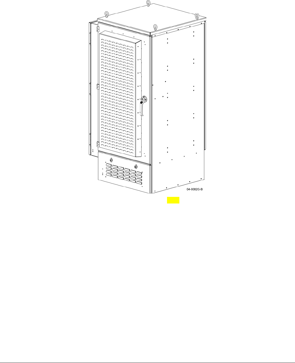
OPAF Front Isometric View and Rear Isometric View
044-05156 Rev C 8
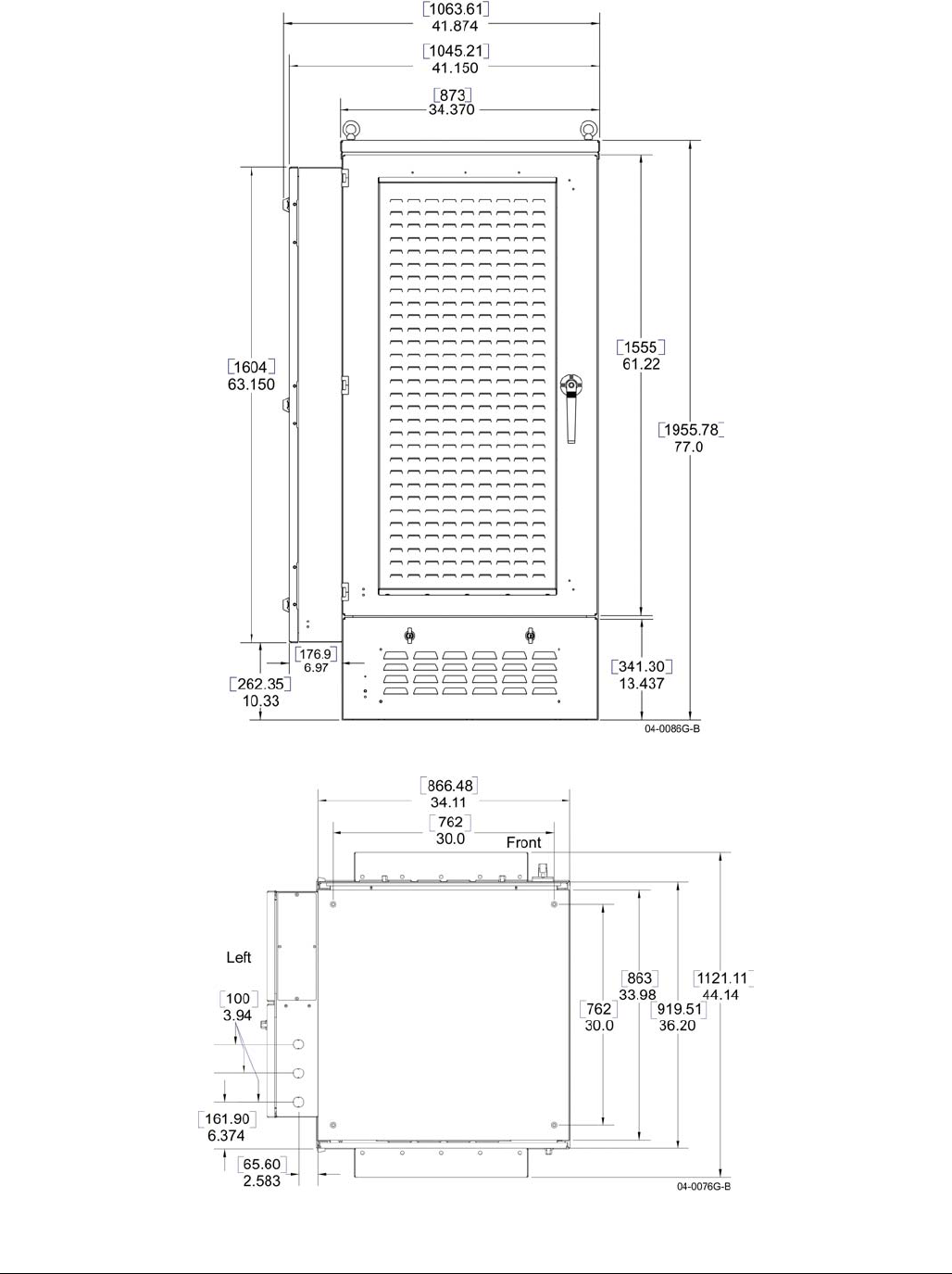
OPAF Front View with Dimensions
OPAF Bottom View with Dimensions
044-05156 Rev C 9
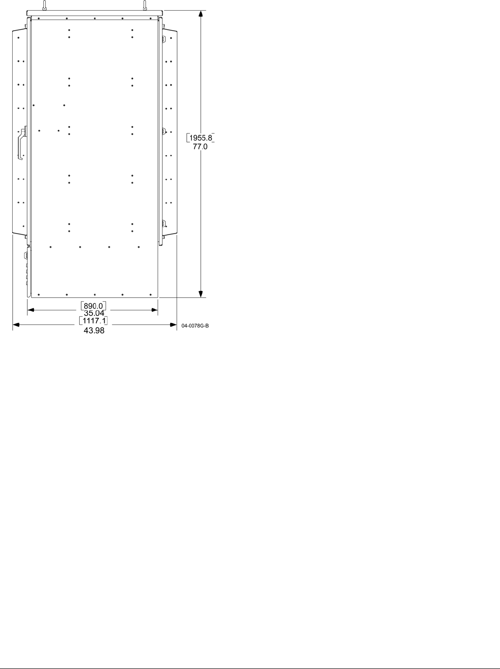
OPAF Left Side View and Right Side with Dimensions
044-05156 Rev C 10
OPAF Front View with Door Removed
044-05156 Rev C 11
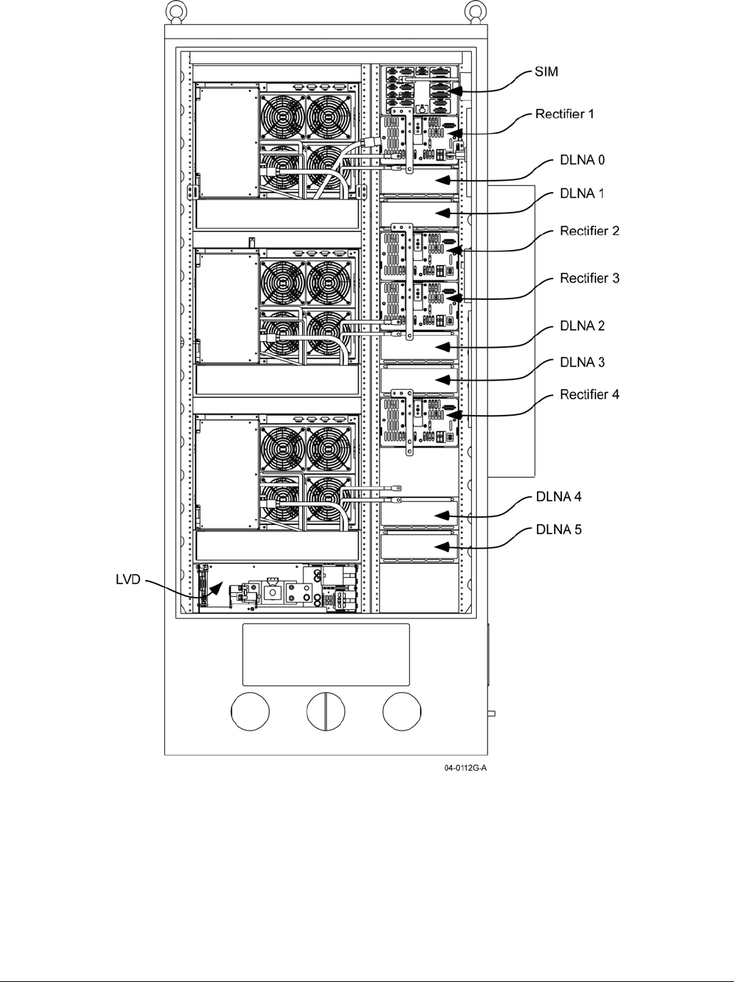
OPAF Rear View with Door Removed
044-05156 Rev C 12
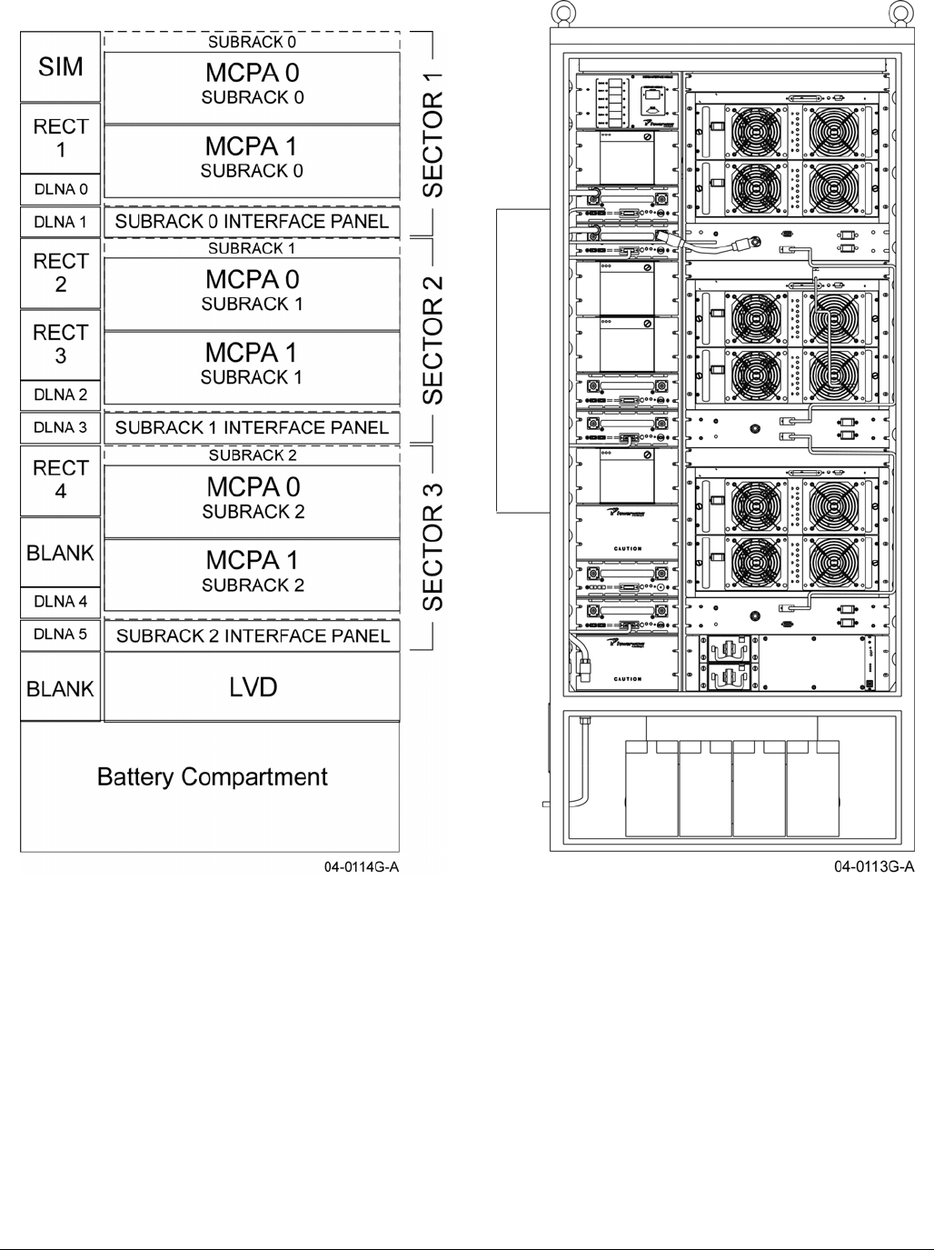
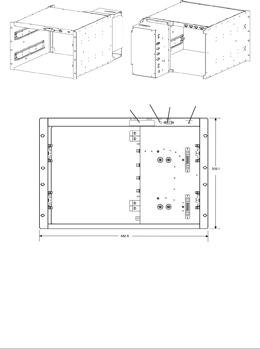
MCR21929-1-2 Subrack Front and Rear Isometric View
MCR21929-1-2 Front View without Amplifiers
Host Address and
Configuration
Switches (Covered)
A
PC LED
Indicato
r
RS232
Port
Gain
A
djust
044-05156 Rev C 13
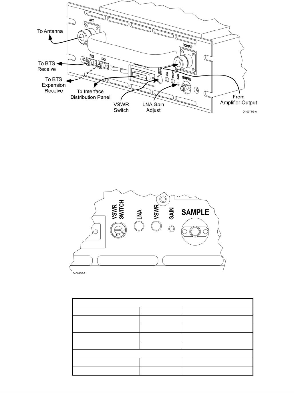
MCR21929-1-2 Subrack Interface Connectors
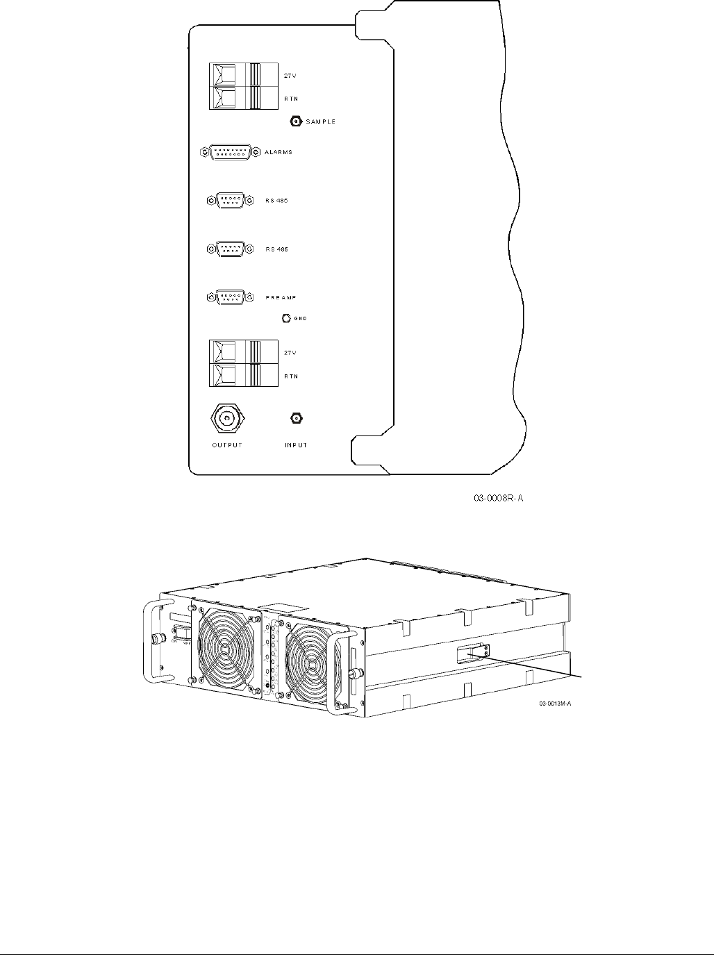
G3S-1900-125 Multi-Carrier Power Amplifier Isometric View
Release
Latch
044-05156 Rev C 14
G3S-1900-125 Multi-Carrier Power Amplifier- Front, Side and Rear Views
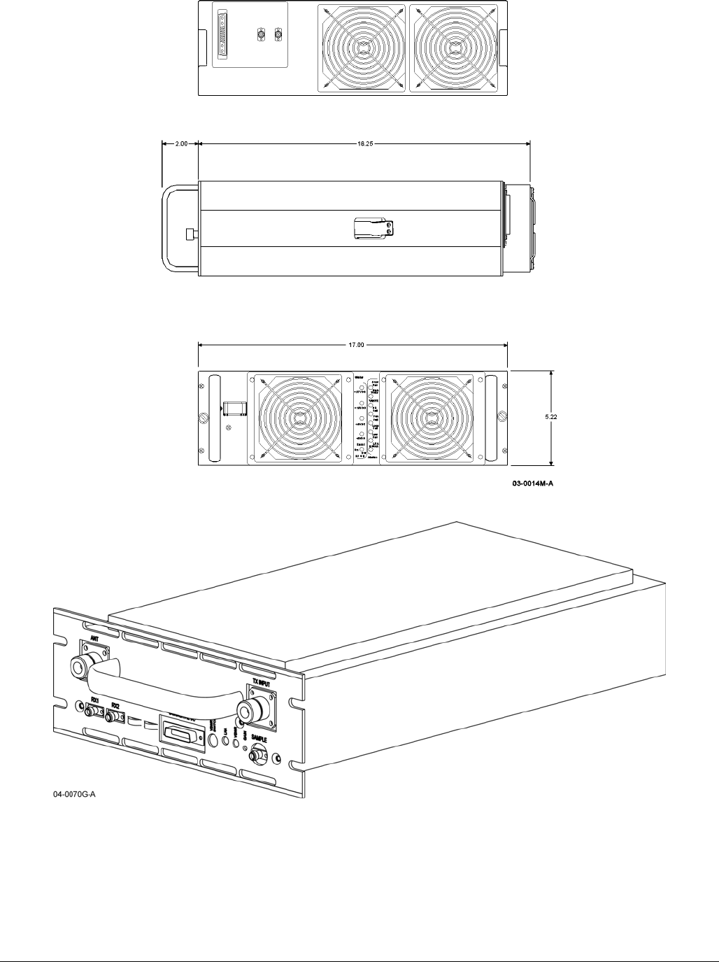
DLNA Dimetric View

044-05156 Rev C 15
DLNA Front Panel
DLNA Side View Panel
System Interface Module
044-05156 Rev C 16
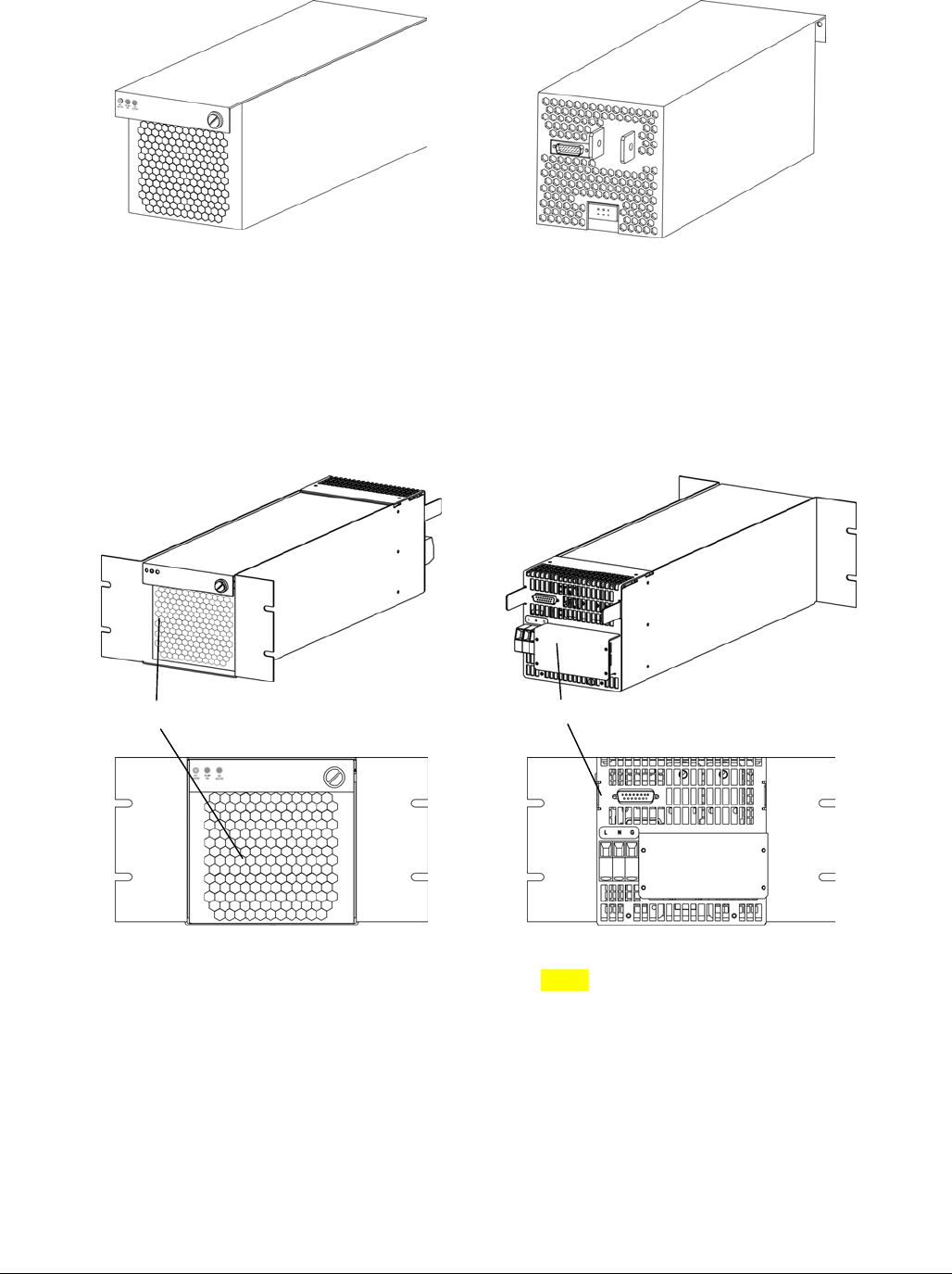
148-Amp Rectifier Isometric Views
148-Amp Rectifier Tray and Panel Views
Front Rea
r
Front Rear
044-05156 Rev C 17
Low Voltage Disconnect (LVD) Module
P/N 920-00337-003 Back-Up Battery
4.1 Cabinet Overview
This section contains a functional description of the Powerwave OPAF Outdoor Multi-Carrier Power Amplifier
(MCPA) System. Refer to the system block diagrams below.
A complete OPAF system consists of a combined three-sector configuration that includes six G3S-1900-125
MCPA, 125-Watt amplifiers and three 4 KW (148-Amp), six Duplexer LNA (DLNA) assemblies, a System Interface
Module (SIM), four 220 VAC AC to +27 VDC rectifiers, a Low Voltage Disconnect (LVD) assembly, four backup
batteries and one outdoor enclosure.
The cabinet is equipped with four lifting bosses on the top panel. The lifting bosses are designed to carry six-times
the weight of the cabinet and its full contents, providing the weight is evenly distributed between the four lifting
bosses.
The cabinet provides easy cable and conduit access, to eliminate the need for external cable protective materials.
This eases the installation and maintenance of the cabinet. The cabinet is designed for ease of maintenance with
most modules and cables accessible either from the front of the cabinet, or side panel maintenance ports.
The cabinet provides 3 110 VAC GFCI courtesy outlets. 2 are incorporated in the front and rear light fixtures at the
top of the cabinet, the third is located inside the AC panel. 10 amps of service is available for these three outlets.
044-05156 Rev C 18
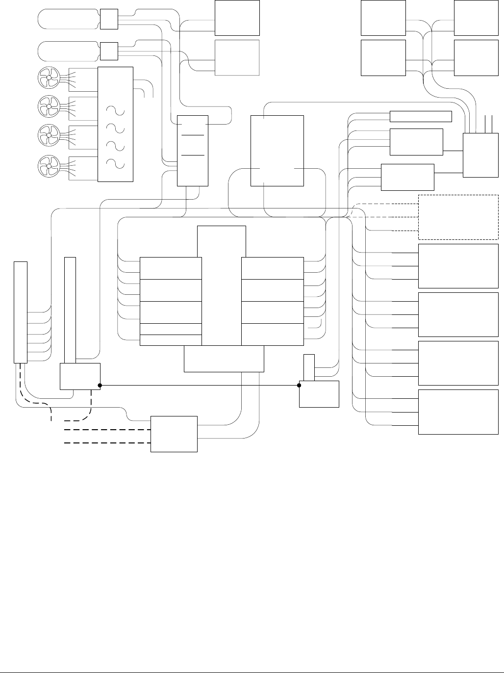
Fan
Module
Main
Bus
4 KW (148 Amp)
Rectifier
930-00018-005
Line
Line
GND
4 KW (148 Amp)
Rectifier
930-00018-005
Line
Line
GND
4 KW (148 Amp)
Rectifier
930-00018-005
Line
Line
GND
4 KW (148 Amp)
Rectifier
930-00018-005
Line
Line
GND
4 KW (148 Amp)
Rectifier
930-00018-005
Line
Line
GND
04-0064W-C
30 A CB 3
Rectifier 1
20 A CB 6
Surge Pro.
30 A CB 7
Rectifier 4
30 A CB 8
Rectifier 5
15 A CB 9
Battery Heater
15 A CB 2 GFCI
GFCI
Outlet AC Relay
Surge
Protector
Battery Heater
Line
Line
EMI Filter
Line
150 A Main
CB 1
30 A CB 4
Rectifier 2
30 A CB 5
Rectifier 3
28
29
26
25
23
22
18, 21
4
7
8
10
11
13
14
4
Load
Line
BLK
GRN
9
7
8
212
10
11
15
13
14
24
22
23
27
25
26
5
1
6 5 4
3 2 1
B A
9 8 7
21
BLK
BLK
GRN
BLK
620
WHT WHT
5
19
30, 31
WHT
BLK
GRN
Batt
Door
N/O
N/C
COM
AC
Door
N/O
N/C
COM
Rear
Door
N/O
N/C
COM
Front
Door
N/O
N/C
COM
F1
F2
F3
F4
47, 48
Light 1
Light 2
43
44
43
44 GRN
49
WHT
50
46
45
45,
46
30
29
31
17
BLK
Ground Bus
9
6
12
15
24
27
3Neutral
Bus
Neu
Line
17
19
Neutral
Bus
*61
GND
Customer
AC Input
*Ground Warning
When connecting to the main service transformer, connect main ground and wire #61 to the Neutral bus.
When connecting to another AC panel, this becomes a sub-panel. Connect main ground to the Ground Bus and disconnect wire #61 at
the Neutral bus. Insulate the bare wires on #61 wire. Failure to disconnect wire #61 may cause a ground loop and a safety hazard,
resulting in injury or equipment damage.
Surge
Protector
SIM
33
BLK
32
BLK
16, 20
34
RED
1
28
2
2
1
18
16
NH
G
NH
S2
N/O
N/C
COM
48
50
S1
N/O
N/C
COM
47
49
Front
Rear
38
36 40
42
37
35 39
41
34
2 RED
1 BLU
3 WHT
4 YEL
2 RED
1 BLU
3 WHT
4 YEL
2 RED
1 BLU
3 WHT
4 YEL
2 RED
1 BLU
3 WHT
4 YEL
To
SIM
To Fan
Module
4.2 AC Power Distribution
Simplexed transmit RF input is provided by the BTS to the OPAF input bulkhead. The transmit signals are
combined (in the 16x16 configuration), amplified, then duplexed with the receive signals. The duplexed signals are
presented to a bulkhead connector for interface with the antenna port. The duplexer provides coupled samples of
the forward and reflected signals for BTS diagnostics.
Received signals from the duplexed antenna are separated from the transmit signals in the DLNA. The receive
signals are amplified by 45 dB through a low noise amplifier. The output signal is split into two paths, to allow for
future system expansion. Each sector has two DLNAs, one for the primary receive path and one for the diversity
receive path. The diversity DLNA only has transmit signals when the sector is expanded beyond eight carriers.
The SIM assembly monitors the MCPAs, LNAs, LVD, and rectifiers, and reports alarms via the I2C and DALI
interface.

044-05156 Rev C 19
System Interface Module
A FE D
B
C
I2CdI2Cm
13
2
FORM-C
6
66 9
99 999
MCR21929-1-2
Max Combined Power 220W (53.4dBm)
+51.5 +/-0.5dB Gain Max
10 dB Dynamic Range
VVA
Controller
G3S-1900-125
Switch
Comb.
S
p
l
i
t
t
e
r
+27VDC GND
Form-C
1
6
To
Controller RS-485
RS-485
VVA_Contro
l
Switch_ Control
L/A
-0.1dB
TX
R
X
DLNA0
Detector
Circuit
FWD
RVS
-3.0dB
-0.1dB
-0.1dB
LNAd
50 Ω
I2C
I2
C
+27VDC
B
9
GND
+12VDC
-0.8dB
TX/RXm
+52.1dBm
+53.3dBm
+53.4dBm
-0.1dB
-0.5dB
-0.3dB
-0.2dB
+49dBm
+21.7dBm Max/Carrier
+30.7dBm Composite
+30.9dBm
-0.2dB+21.7dBm Max/Carrier
+30.7dBm Composite
TX:
+52.0dBm (160W)
8 Carriers @ +43.0dBm/Carrier
RX:
-23.0dBm Max/Carrier
-14.0dBm Composite
+4.7dBm
+5.2dBm
Composite
8 Carriers @
-3.8dBm/Carrier
Power from S-
New Cabinet
with Cable
Loss
VVA Set @
-2.8dB
to achieve
max RF
output
RXd
A
N
T
RS-485
To
2nd
MCPA
TX
R
X
DLNA1
Detector
Circuit
FWD
RVS
-3.0dB
-0.1dB
-0.1dB
LNAd
50 Ω
I2C
I2
C
9
+12VDC
-0.8dB
+53.3dBm
-0.3dB
+49dBm
+30.9dBm
A
N
T
A
04-0065B-B
G3S-1900-125
+27VDC
GND
Antenna Power Levels:
L/A
-0.1dB
OPAF-1923-P07C01 RF Configuration, Single Sector Example
4.3 RF Input Signal
Any number of RF input signals can be applied to the transmit RF input port, providing: the signals meet
established mask requirements for any 2G or 3G wireless modulation scheme, the input signals do not cause the
amplifier to be over driven, and the gain of the system meets the appropriate base station architechural
requirements. The maximum input power for all carrier frequencies should not exceed the limits idicated in the
system specification. The input VSWR should be 2:1 maximum (or better).
4.4 RF Output Load
The load impedance should be as good as possible (1.5:1 or better) in the working band for good power transfer to
the load. The amplifier is operated into a duplexer and will maintain its distortion characteristics outside the signal
band even if the VSWR is infinite, provided the reflected power does not exceed one watt. A parasitic signal of less
than one-watt incident on the output will not cause distortion at a higher level than the normal forward distortion (i.e.
-63 dBc).
044-05156 Rev C 20
4.5 G3S-1900-125 Amplifier Module
4.5.1 Overview
The G3S-1900-125 amplifier is a linear, feed-forward power amplifier that operates in the 60 MHz frequency band
from 1930 MHz to 1990 MHz. It is designed to operate in two continuous frequency blocks in the PCS band or an
instantaneous bandwidth of 20 MHz. A typical one-sector system is illustrated above. Each amplifier is a self-
contained plug-in module and is functionally independent of the other amplifier module. The amplifier modules are
designed for parallel operation to achieve high peak power output, and for redundancy in unmanned remote
locations. Each amplifier in the system can simultaneously transmit multiple carrier frequencies at 85 watts per
sector, for a combined output power of 170 watts.
Each amplifier output is an amplified composite signal of approximately 125 watts before losses. All phase and gain
corrections are performed on the signal(s) in the individual amplifier modules. Each amplifier module has alarm and
display LEDs that display the amplifier performance. If a failure or fault occurs in an amplifier module, it is displayed
on the individual amplifier front panel.
The amplifier typically draws 52 amps of current at rated output power, and approximately 25 amps with no RF
signals applied. Be sure to turn the amplifier off before removing it from the subrack to avoid damaging the
equipment or causing personal injury.
4.5.1.1 Controls, Indicators, & Interfaces
Primary +27 Vdc power is applied to the amplifier via a 100-amp circuit breaker (ON-OFF) located on the left side of
the amplifier front panel.
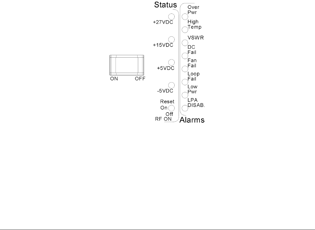
The plug-in amplifier module RF control and indicators, located in the center of the amplifier front panel between
the cooling fans, are shown below. The status and RF control functions are described in detail in the Amplifier
Module DC Indicators RF Switch Definition table. The alarms are described in detail in the Amplifier Module RF
Control and Indicators Definition table.
G3S-1900-125 Amplifier Module RF Control and Indicators

044-05156 Rev C 21
Amplifier Module DC Indicators RF Switch Definition
Name Function
+27VDC
Indicator
Green LED. When lit, indicates that the +27 Vdc supply is greater than +21 Vdc and less than +31
Vdc. If the +27 Vdc indicator goes out, the DC Fail indicator will illuminate. This indicates that the +27
Vdc voltage dropped below +21 Vdc.
+15VDC
Indicator
Green LED. When lit, indicates that the +15 Vdc supply is greater than +12 Vdc and less than +17
Vdc. If the +15 Vdc indicator goes out, the DC Fail indicator will illuminate. This indicates that the +15
Vdc voltage dropped below +12 Vdc or increased above +17 Vdc.
+5VDC
Indicator
Green LED. When lit, indicates that the +5 Vdc supply is greater than +2 Vdc and less than +7 Vdc. If
the +5 Vdc indicator goes out, the DC Fail indicator will illuminate. This indicates that the +5 Vdc
voltage dropped below +2 Vdc or increased above +7 Vdc.
-5VDC
Indicator
Green LED. When lit, indicates that the -5 Vdc supply is greater than -7 Vdc and less than -2 Vdc. If
the -5 Vdc indicator goes out, the DC Fail indicator will illuminate. This indicates that the -5 Vdc
voltage dropped below -7 Vdc or increased above -2 Vdc.
RF ON
Switch
Three position switch:
Off (down position) - Turns off amplifier module.
On (center position) - Normal amplifier on position.
Reset (up position) - When toggled to reset position, all the red LED indicators will turn on one at a
time in sequence followed by all the green indicators one at a time in sequence; this will also reset the
fault latches. If the switch is held in the reset position, a microcontroller reset will occur. This will be
verified by the LEDs toggling state again. The switch is spring loaded to return to the normal ON
position when released. If a fault occurs and the MCPA is disabled, the alarms can be cleared and the
MCPA enabled by this reset position. The functions of the switch are disabled for five seconds after a
power-up condition.

044-05156 Rev C 22
Amplifier Module RF Control and Indicators Definition
Amplifier
Alarm Latching LED MCPA
Module
System
Alarm
(From
Subrack)
MCPA
Disable signal
(pin 4)
Condition Auto-
Recovery
Over PWR
Fault Yes Red Disable Major High MCPA Module Pout
> 52 dBm (Note 1) None
Over PWR
Fault No Red Disable Major High Pin > -6 dBm software; -
5 dBm hardware
<-12 dBm
Software
High
Temperature No Red Enable None Low Base plate
temperature > 80 C <75°C
High
Temperature No Red Disable Major High Base plate temperature
> 85 C <75°C
VSWR No Red Enable None Low
Reflected and Forward
Powers both exceed
40W. Condition exist for
less than 1 minute
Reflected or
Forward Power
< 38W
VSWR Yes Red Disable Major High
Alarm set after alarm
state on for more than 1
minute
None
DC Fail No Red Disable Major High Average Internal
voltage out of range. (Note 2)
DC Fail
(Over
Voltage)
No Red Disable Major High +27V DC input
> 30.5 V 30.0V
DC Fail
(Under
Voltage)
No Red Disable Major High +27VCD input < 21 V 21.5V
Fan Fail No Red Enable Minor Low Any fan fail (<70 Hz
Speed)
(>100 Hz
Speed)
Loop Fail Yes Red Disable Major High Loop fail detected longer
than 2 min None
Low PWR N/A Red Enable None Low
Indication shown base
on rack RS 485
command.
NA
MCPA Module Alarm Definition:
Note 1: When Over Power detected at the output:
a) MCPA Module will shut down (Disable).
b) Turn on red Over Power lamp.
c) Latch Over Power alarm
d) The MCPA Module will use a RMS detector to determine the over power fault.
Note 2: The Appropriate Status lamp will turn off, indicating which voltage is out of its range.
(10% range for +15V, +5V, and -5V).
The amplifier module has an average output of 125 watts power (1250 watts peak power) with intermodulation
products suppressed to better than -63 dBc below carrier levels. The amplifier provides an amplified output signal
with constant gain and phase by adding approximately 25 dB of distortion cancellation on the output signal.
Constant gain and phase is maintained by continuously comparing active paths with passive references, and
correcting for small variations through the RF feedback controls. All gain and phase variations, for example those
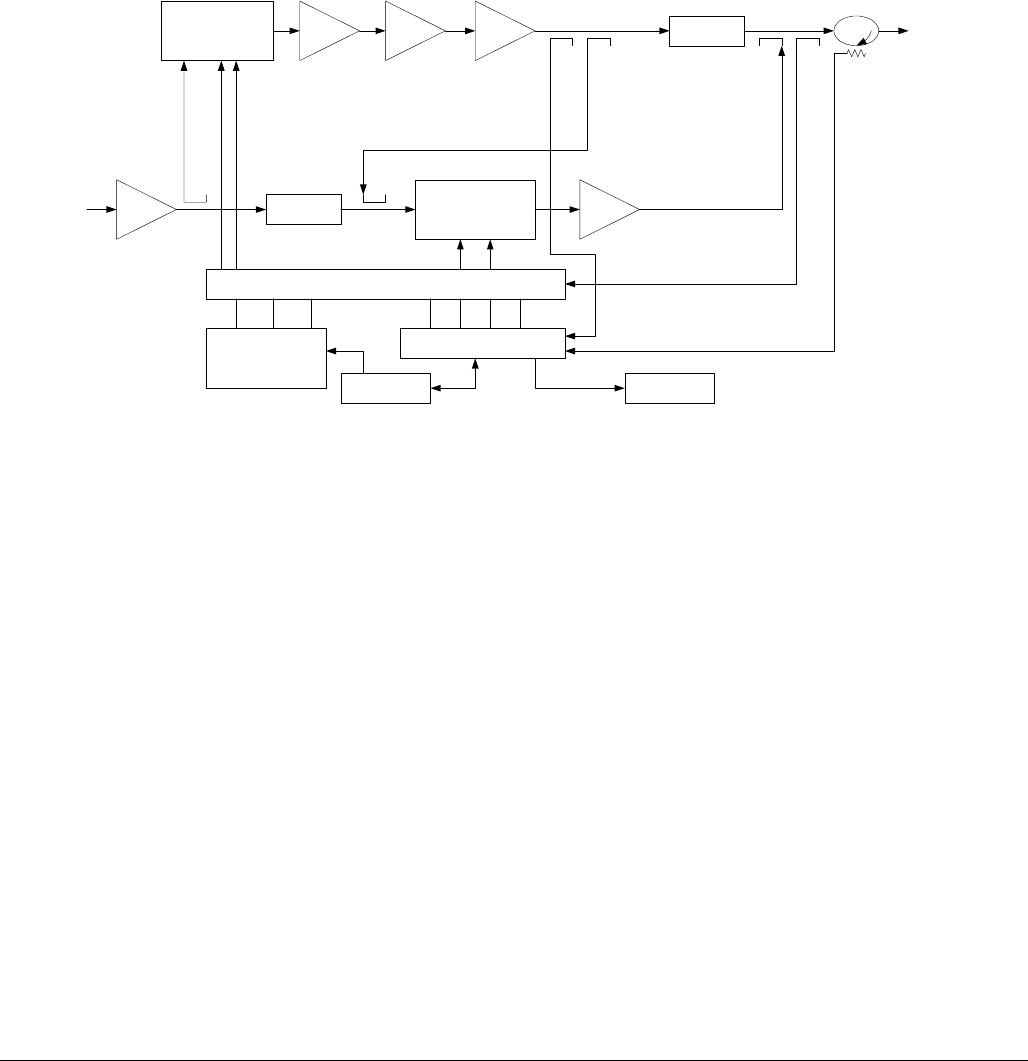
due to temperature, are reduced to the passive reference variations. The amplifier module is comprised of:
Preamplifiers Two feed-forward loops with phase-shift and gain controls
Main amplifier DC/DC power regulator
Error amplifier Alarm monitoring, control, and display panel
044-05156 Rev C 23
4.5.1.2 Main Amplifier
The main amplifier employs class AB amplification for maximum efficiency. The error amplifier and feed forward
loops are employed to correct signal nonlinearities introduced by the class AB main amplifier. The error amplifier
operates in class AB mode. The RF input signals are amplified by a preamp and coupled to an attenuator and
phase shifter in the first feed-forward loop. The main signal is phase shifted by 180 degrees and amplified in the
premain amplifier. The output from the premain amplifier is fed to the class AB main amplifier. The output from the
main amplifier is typically 180 watts. The signal is output to several couplers and a delay line.
The signal output from the main amplifier is sampled using a coupler, and the sample signal is combined with the
main input signal and input to the second feed-forward loop. The error signal is attenuated, phase shifted 180
degrees, then fed to the error amplifier where it is amplified to a level identical to the sampled output from the main
amplifier. The output from the error amplifier is then coupled back and added to the output from the main amplifier.
The control loops continuously make adjustments to cancel out any distortion in the final output signals.
Pre
Amp
Pre
Main
Main
Amp
Error
Amp
Delay
Feed Forward Loop control
2nd Loop
Phase & Gain
1st Loop
Phase & Gain Delay
Alarms & Display
+15 +5 -5
Power Supply
RF Out
RFL
PWR
FWD
PWR
Front Panel
Smart Rack
+27VDC
Pre
Dist
Phase
& Gain
G3S-1900-125 Power Amplifier Module Functional Block Diagram
The 2nd loop control section obtains a sample of the distortion added to the output signals by the main amplifiers,
phase shifts the signals by 180 degrees, then feeds it to the error amplifier. There it is amplified to the same power
level as the input sample and coupled on to the main output signal. The final output is monitored by the 2nd loop
and adjusted to ensure that the signal distortion and IMD on the final output is canceled out.
The input and output of the amplifier employ two-stage, class AB amplifiers, which provide approximately 25 dB of
gain in the 60 MHz frequency band from 1930 to 1990 MHz. The amplifier operates on +27 Vdc, and is mounted
directly on a heat sink, which is temperature monitored by a thermal sensor. If the heat sink temperature exceeds
85°C, a high temperature fault occurs. The alarm logic controls the transistor bias voltage, which shuts down the
amplifier.
4.5.1.3 Error Amplifier
The main function of the error amplifier is to sample and amplify the signal distortion level generated by the main
amplifier, to a level that cancels out the distortion and IMD when the error signal is coupled onto the main signal at
the amplifier output. The error amplifier is a balanced multistage, class AB amplifier, has 75 dB of gain, and
produces over 100-watts peak output. The amplifier operates on +27 Vdc and is mounted directly on a heat sink.
4.5.1.4 Amplifier Monitoring
In the main and error amplifier modules, all normal variations are automatically compensated for by the feedforward
loop control. However, when large variations occur beyond the adjustment range of the loop control, a loop fault
will occur. The alarms are displayed on the front panel indicators and output via a 21-pin connector on the rear of
the module to the subrack summary board for subsequent remote monitoring via the ALARMS connector.
4.5.2 Amplifier Module Cooling
044-05156 Rev C 24
Although each amplifier module contains its own heat sink, it is cooled with forced air. Four fans are used for
forced air cooling and redundancy. The fans, located on the front and rear of the amplifier module, draw air in
through the front of the amplifier and exhaust hot air out the back of the module. The fans are field replaceable.
4.5.3 Intermodulation
The G3S-1900-125 amplifier is designed to deliver a 125-watt composite average power, multicarrier signal,
occupying a bandwidth less than or equal to 20 MHz, in the bandwidth from 1930 to 1990 MHz. The maximum
average power for linear operation, and thus the amplifier efficiency, will depend on the type of signal amplified.
4.5.3.1 Two Tone Intermodulation
When measured with two equal CW tones spaced anywhere from 30 kHz to 20 MHz apart, and at any power level
up to the average power, the third order intermodulation products will be below -63 dBc
4.5.3.2 Multitone Intermodulation
Adding more tones to the signal will lower individual intermodulation products. If the frequencies are not equally
spaced, the level of intermodulation products gets very low. When the frequencies are equally spaced, those
products fall on top of each other on the same frequency grid. The average power of all intermodulation beats
falling on the same frequency is called the composite intermodulation; it is -63 dBc or better.
4.5.4 Amplifier Monitoring
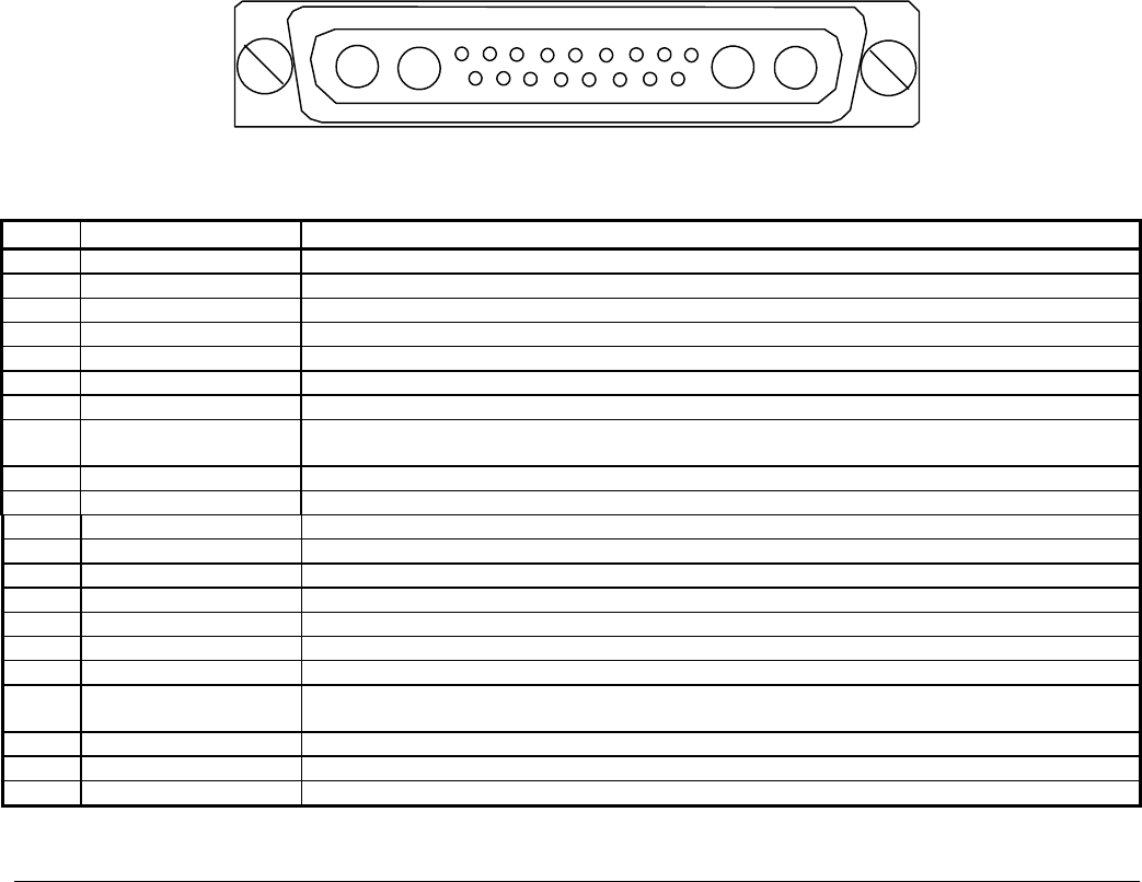
The amplifier has a separate remote alarm and control connector, which may be used by the host system to
monitor and control the individual amplifier modules. The status, alarm, control, and power connections on the
amplifier connector are made through a 21-pin male D-Sub combo connector and are listed and described in the
Amplifier Module DC and Logic Connector Definition table.
A1 A2 A3 A4
1 2 3 4 5 6 7 8 9
10 11 12 13 14 15 16 17
DC and Logic Connector (Male, on Rear of G3S-1900-125 Amplifier Module]
Amplifier Module DC and Logic Connector Definition
PIN Function Description
A1 Power Input +27 Vdc (Power Contact)
A2 Power Input +27 Vdc (Power Contact)
A3 Ground Ground (Power Contact)
A4 Ground Ground (Power Contact)
1 RS485 +TxD Serial Communication Data Out
2 RS485 +RxD Serial Communication Data In
3 Service Loop TTL input to Amp. Gnd. for special test mode (Note 1)
4 MCPA Disabled
(Summary Fault)
TTL signal normally low indicates MCPA enabled. A high level indicates that the MCPA has
been disabled. Over Power, Over Voltage takes one second to activate the signal.
5 Mod Addr 0 TTL input to Amp. Gnd. supplied by shelf to identify slot.
6 Mod Addr 1 TTL input to Amp. Gnd. supplied by shelf to identify slot.
7 TP1 TTL output. Future test point.
8 Manual Download GND to download manually
9 DC on stat TTL output. High indicates Amp is powered on.
10 RS485 –TxD Serial Communication Data Out
11 RS485 –RxD Serial Communication Data In
12 SCL7 No connection
13 SDA7 No connection
14 FP Disable Output Output, GND if the front panel switch is in the OFF position; +5 volts indicates the front panel
switch is in the ON position.
15 FP RST Output, GND if the front panel switch is in the RESET position; +5 volts otherwise.
16 GND Ground
17 Module Detect Ground potential. Informs the subrack that an MCPA is plugged in.

044-05156 Rev C 25
Note 1: Service loop grounded allows the MCPA to be enabled or disabled by the front panel switch when not
mounted in the shelf.
4.5.5 Pilot Tone Control
The multi-amplifier subracks can be used to control the pilot tone frequency of the installed amplifiers. Pilot tone
frequency selection is based on the intended operational band of the amplifiers per the following table.
Pilot Frequency Setting Based on PCS Frequency Block of Operation
Transmit Frequency Band (MHz)
Block Designator Base Station Bandwidth Pilot (MHz)
A 1930-1945 15 1945.5 (A)
D 1945-1950 5 1950.5 (D)
B 1950-1965 15 1965.5 (B)
E 1965-1970 5 1964.5 (E)
5 1965-1970 5 1970.5 (5)
F 1970-1975 5 1969.5 (F)
C 1975-1990 15 1974.5 (C)
Block Pairs
A-D 1930-1950 20 1950.5 (D)
D-B 1945-1965 20 1965.5 (B)
B-E 1950-1970 20 1970.5 (5)
E-F 1965-1975 10 1964.5 (E)
F-C 1970-1990 20 1969.5 (F)
E-C Excluding F 1965-1990 Excluding: 1970-1975 25 1974.5 (C)
Notes:
1. If the Block Designator has not been previously selected through serial communication on connector
J10M, pilot defaults to 1960.5 MHz on the G3S-1900-80 amplifier; 1964.5 on the G3S-1900-125
amplifier
2. If the Block Designator is selected through serial interface on connector J10M, pilot frequency is moved
to the appropriate spot and is stored permanently into the microprocessor until another band is
changed.
If the pilot tone is not moved and signals are transmitted in B-band, some traffic channels may transmit directly on
the pilot tone. The pilot tone requires a guard band of 60 KHz for TDMA, 270 KHz for CDMA (IS-95), and 400 KHz
for GSM. Transmitting on the pilot tone will cause the amplifier to go into Loop Fail. This will not damage the MCPA.
However, CDMA customers will experience a Loop Fail in every sector where the amplifiers are installed. TDMA
and GSM customers will experience intermittent Loop Fails in the sectors that use these frequencies.
On the other hand, if the pilot tone is not moved and signals are transmitted in A-band (1930-1945) or C-band
(1975-1990), the instantaneous bandwidth of the amplifier will be exceeded. This will cause equipment operated in
the outer bands of the PCS band to experience higher intermodulation distortion, which may in turn cause them to
exceed FCC emission limits. The lower end of the PCS band presents the farthest frequency span from the pilot
tone, which begins at 1930 MHz; 30.5 MHz away from the pilot tone of the G3S-1900-80 amplifier; 34.5 MHz away
from the pilot tone of the G3S-1900-125 amplifier.
Setting the pilot tone frequency of the amplifiers requires a laptop interface program. The laptop can be connected
to the multi-amplifier subrack’s RS-232 port. The multi-amplifier subrack provides the interface to the amplifiers to
set their pilot frequency and stores this setting in memory. If an amplifier fails, the multi-amplifier subrack programs
the pilot frequency of the replacement amplifier to that of the other installed amplifiers.
Refer to the Site Preparation and Installation Manual or Field Replaceable Units manual for the pilot tone
configuration procedure. Contact Powerwave to obtain a copy of the program and related instructions.

044-05156 Rev C 26
4.6 MCR21929-1-2 Amplifier Subrack
4.6.1 Overview
The MCPA system is a linear, feed-forward power amplifier system that operates in the 60 MHz frequency band
from 1930 to 1990 MHz with an instantaneous bandwidth of 20 MHz. It consists of an amplifier subrack with up to
two 125-watt G3S-1900-125 plug-in amplifiers.
The MCR21929-1-2 houses an RF power splitter/combiner and a control module that monitors the functional status
of all plug-in amplifiers. Additionally, the subrack is equipped with an Automatic Power Control (APC) circuit and an
RF GAIN ADJUST potentiometer. The APC indicator and GAIN ADJUST potentiometer are located on the upper
front of the subrack as shown below. Each subrack provides two RS-485 alarm interface ports, a preamp alarm
interface port, a Form-C alarm interface port and an RS-232 maintenance port, as well as, RF IN, RF OUT and a
–50dB RF sample port. Only the two RS-485 alarm interface ports are used to report alarm status to the SIM.
Subrack alarms are daisy chained together and address switches on the front panel are set to identify the
appropriate sector.
When two of the same model amplifiers are used, the system offers up to 218 watts of output power (after combiner
insertion losses) using the 125-watt amplifier.
MCR21929-1-2 (Reach-through (Pseudo) Front Access) - This 19-inch flush mount subrack has front “reach
through” access to its interconnect panel located at the rear of the subrack.
4.6.1.1 Controls, Indicators, & Interfaces
The location and function of the amplifier subrack controls and indicators is depicted below and described in the
paragraphs that follow.
MCR21929-1-2 Controls and Indicators
4.6.1.1.1 AO A3 (Address) Switch
This four-position DIP switch is used for setting the external RS-485 alarm bus address.
MCR21929-1-2 Address Switches
4.6.1.1.2 Config Switch
This four-position DIP switch is used for selecting software features in the amplifier subrack. Refer to Gain Modes
later in this section for a description. Preamplifiers are not used in this system, so the second dip switch is set to
Off, as indicated below in the left two diagrams.
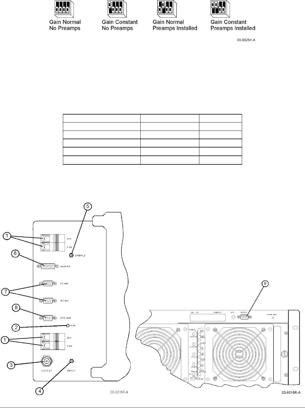
044-05156 Rev C 27
MCR21919-1-2 Configuration Switch
4.6.1.1.3 APC LED
The LED indicator located on the top right-hand corner of the subrack serves several functions. Under normal
conditions, the indicator is off. Anytime the APC function is engaged, either from an overdrive or voltage derating
situation, the indicator blinks. When the overdrive or voltage derating condition is removed and all the gain is
recovered, the indicator ceases to blink and remains off. During maintenance functions such as downloading
firmware and detector calibration, the indicator blinks to signify the beginning and end of those functions.
APC LED Sequence and Blink Rate
Operation Sequence Blink Rate
APC due to an overdrive On/Off 1 Hz
APC due to an over voltage On/Off/Off/On 1 Hz
APC due to an under voltage On/Off/Off/On 1 Hz
System firmware upgrade On/Off 0.1 Hz
Detector calibration On/Off 1 Hz
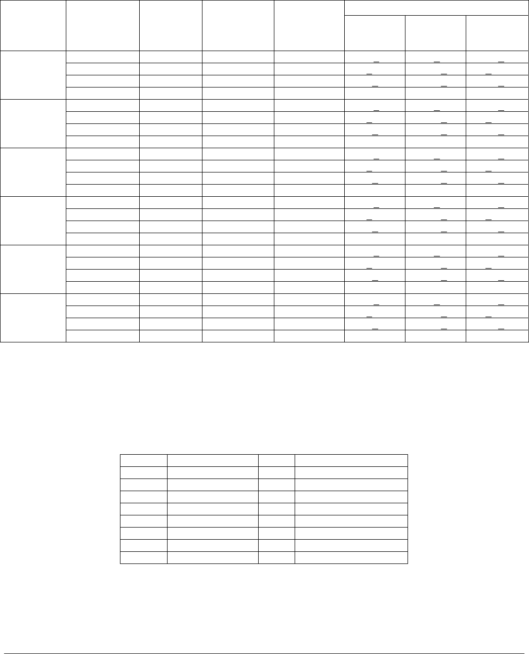
4.6.1.1.4 Gain Adjust
This potentiometer allows the subrack gain to be attenuated 0 to 10 dB in Normal operating mode, or 0 to 3 dB in
Constant Gain operation mode. Refer to Gain Modes later in this section.
044-05156 Rev C 28
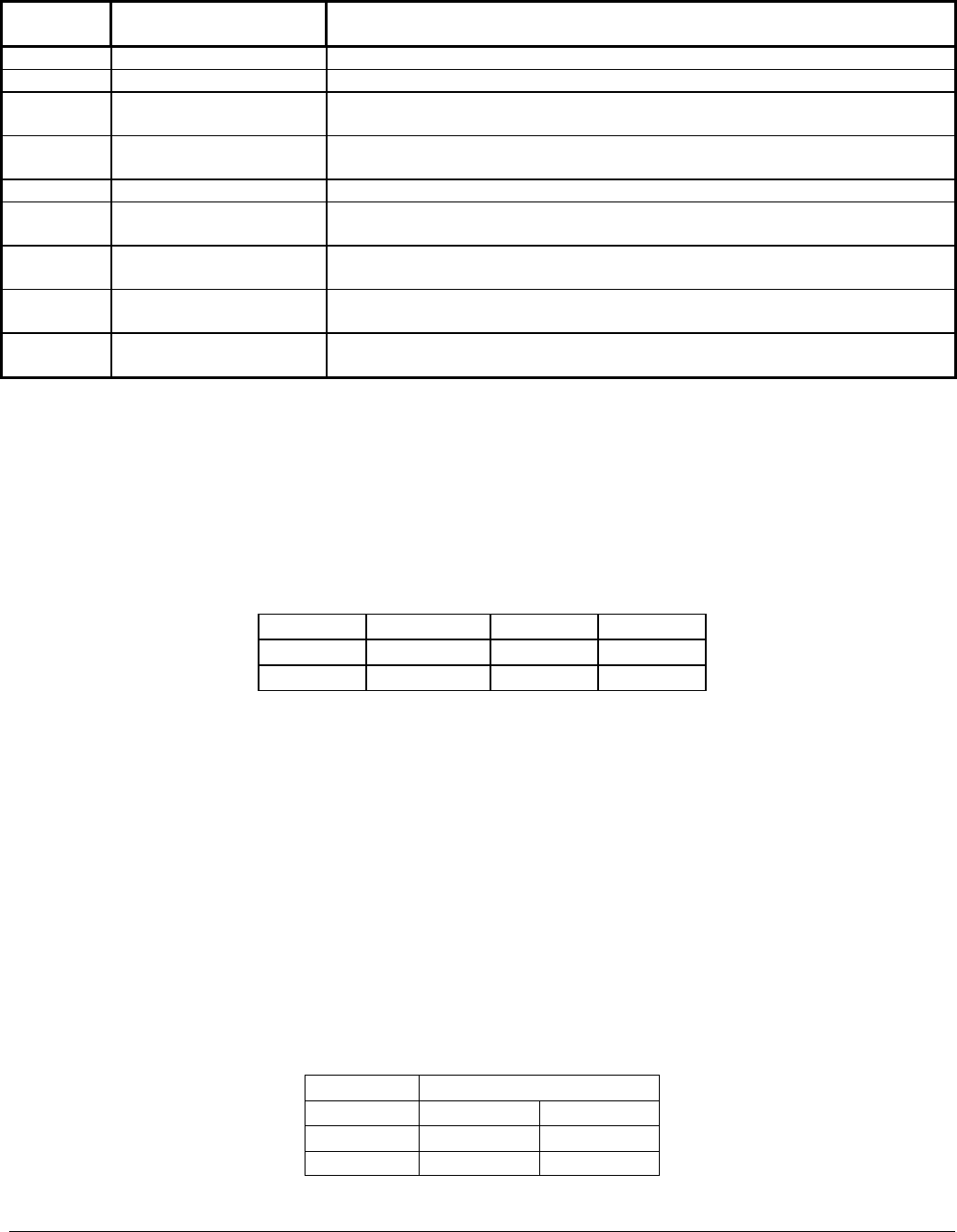
MCR21929-1-2 Subrack Input/Output Connectors
Reference
Number Name Function
1 DC Power Terminals Base station DC power connections.
2 GROUND Lug Subrack chassis ground.
3 RF OUTPUT Connector
Type-N female coax connector, RF output to TX filter and antenna. See
table A-1 for power output level of one to two amplifier module systems.
4 RF INPUT Connector SMA female coax connector. RF input from combiner or TX card. See
specifications for power input level.
5 RF SAMPLE Connector SMA female coax connector. ~ –50 dB sample of the subrack RF output.
6 ALARMS Connector
15-pin female D-Sub connector. Permits remote monitoring of amplifier
form-C dry contact alarms.
7 RS-485 Connectors
9-pin female D-Sub connector. Permits remote monitoring of RS-485
signals.
8 PREAMP Connector
9-pin female D-Sub connector. Permits remote monitoring of preamplifier
and DC converter signals.
9 RS-232 Connector
9-pin female D-Sub connector. Permits downloading of software to the
subrack and/or amplifiers.
4.6.2 Automatic Power Control (APC)
The APC is a power limiting function that limits the composite output power to 0.2dB to 1.0dB greater than the rated
power for the inserted MCPA combinations. If the output power of the subrack exceeds an “engage” threshold (see
below) the gain is reduced. The LED indicator located on the top front-right of the subrack blinks when the APC is
engaged. The gain is reduced until the output power complies with the “settle” range threshold. As the input drive
reduces, the gain recovers by the amount needed to approach the nominal output power, until the original gain is
achieved. Any power level in between the nominal and the engage threshold does not warrant a gain change.
APC Limit Thresholds (Watts)(G3S-1900-125)
MCPAs Nominal Engage Settle
1 109 122 112
2 218 244 222
4.6.3 Gain Modes
The subrack can be operated in either standard gain or constant gain mode. The choice of two gain modes
provides system design flexibility. Standard gain is the mode most often selected by system designers and is the
factory default setting of the subrack. Standard gain mode changes the gain of a subrack based on the number of
installed functional modules, while constant gain restricts the gain of the subrack to that of about one module,
regardless of the number of modules installed.
When a given sector is operated at full available power to maximize call capacity or when more system gain is
needed, standard gain mode is best. At lower power level requirements or when a specific system gain value must
be maintained, the system designer may elect to use constant gain mode instead. Constant gain mode maintains a
consistent cell site coverage footprint while allowing N+1 redundancy and increased system reliability. By installing
one more amplifier than the RF power plan requires, Constant gain mode allows for a back-up amplifier, should one
of the cell site’s amplifiers become inoperable.
Standard gain or constant gain is independently selectable on a sector-by-sector basis.
Subrack Gain
Active Gain Mode
MCPAs Standard
Constant
2 51.5 48
1 48.5 48

044-05156 Rev C 29
4.6.3.1 Standard Gain Overview and Application (Default Configuration)
In the standard gain mode, the gain of the system is dependent on the number of amplifiers operating at a given
time and the power from the amplifiers is used at or near their maximum limits. When the design of the cell site
requires full power from the amplifiers installed in the subrack in order to achieve maximum call capacity, the
standard gain mode should be used. For example, if the sector design calls for 150 watts (measured at the
directional coupler output; assuming 1.5 dB of loss from the subrack to the directional coupler), the sector should
be configured with two 125 watt amplifiers (154 watts at directional coupler; 51.5 dB subrack system gain) to take
full advantage of the available power. The trade-off here, is that if an amplifier fails, the available power drops back
to 77 watts, the overall gain drops by 3.0 dB, and all the transmit channel powers drop by 3.0 dB as well (i.e. 7.5
watts to 3.75 watts per channel).
Gain adjustment via the front panel potentiometer is available.
4.6.3.2 Constant Gain Overview and Application
In constant gain mode, the gain of the subrack remains the same, regardless of the number of amplifiers installed.
Good engineering practice requires careful planning when using constant gain mode. When the design of the cell
site requires much less than maximum power, but must maintain a specific radius of coverage, constant gain mode
is ideal. For example, if the sector design calls for 75 watts output power at the directional coupler, the sector must
be configured with two 125 watt amplifiers (87 watts; 48 dB gain) when constant gain is enabled to allow for
amplifier failure. If an amplifier fails, the available power drops back to 43 watts, the subrack gain adjusts to remain
48 dB (77 watts), and all the transmit channel powers remain at the set power (i.e. 7.5 watts per channel).
However, while in constant gain mode, if the sector power is set to maximum (i.e. 100 watts with two amplifiers
installed), and an amplifier fails, the remaining amplifier will be over-driven and likely to go into an over power
condition. Should this occur, the sector would go into APC control, the input power is attenuated (see paragraph 4-
5), the sector’s footprint shrinks and an alarm is sent to the switch.
Gain adjustment via the front panel potentiometer is available.
4.6.3.3 Gain Mode Control and Theory
The MCR21929-1-2 subrack adds 3 dB of attenuation when constant gain mode is initially activated, reducing the
system gain of the MCR21929-1-2 from a nominal of 51.5 dB to 48.5 dB. Therefore, whenever the gain mode is
changed from standard gain to constant gain or visa-versa, the cell technician must reset the overall system gain or
individual channel power.
In constant gain mode, the gain of each carrier (or the system) must remain constant to avoid reducing the cell
radius. When the subrack detects an amplifier failure, the amplifier subrack reduces input attenuation through the
Voltage Variable Attenuator (VVA) by the amount of gain lost while the amplifier is removed from the circuit. This
allows the system gain to remain constant, and allows the cell site to maintain a consistent footprint. When the
replaced MCPA is enabled, attenuation is again added to the input port of the subrack by the amount of gain
introduced by the replacement MCPA to maintain an overall subrack constant gain.
As MCPAs are disabled and enabled, system gain is recovered within a 1-second time frame. The subrack is
shipped from the factory with the configuration switch set for Standard Gain mode active.
4.6.4 Performance Derating With Lower Supply Voltage
The MCPA system will operate at full power, while meeting all spectrum requirements, over a supply voltage range
of 26 to 28 VDC. The MCPA System will meet derated spectrum requirements at derated output power levels over
a supply voltage range of 21 to 30 VDC. MCPA System power derating levels are outlined in below. The LED
indicator located on the top front right of the subrack blinks when the output power is derated.
Power Derating Versus Voltage Profile
Supply Voltage[VDC] Output Power Derating
28V ≤ V < 30V 0.5dB
26V ≤ V < 28V 0dB
24V ≤ V < 26V 0.5dB
22V ≤ V < 24V 1.0dB
21V ≤ V < 22V 1.5dB
044-05156 Rev C 30
As the voltage returns to nominal levels, the output power will return accordingly. Sufficient hysteresis of at least 0.1
V is included to eliminate 'toggling' at crossover voltage levels.
4.6.5 Amplifier Monitoring
The amplifier alarms are displayed on the front panel indicators and output via a 21-pin connector on the rear of the
module to the subrack summary board for subsequent remote monitoring via the ALARMS connector. The subrack
interprets the amplifier alarms, reacts accordingly, and provides alarm status to the base station through both the
Form-C and RS-485 alarm bus.
Amplifier alarms may be monitored through the dry contact ALARMS 15-pin female D-sub connector on the rear of
the subrack. Refer to Alarm States and ALARMS Connector Definition tables and alarm connector figures below
for pin definition of the alarms connector.
Alarm States
Form-C RS-485
Minor Major Critical Major Critical Minor Major Critical
MCAs
Installed
MCAs
Enabled Pre-
amp
Pre-
amp
2 2 0 0 0 0
2 1 1 0 1 0
2 0 1 1 0 1
1 1 0 0 0 0
1 0 1 1 0 1
One Fan Fault 1 1
No Fan Fault 0 0
No Preamp Fault 0 0 0 0
One Side Preamp Fault 1 0 1 0
O
P
T
I
O
N
A
L Both Sides Preamp Fault 1 1 0 1
0 = Low (no alarm)
1 = High (alarm)
4.6.5.1 Form C Alarms (not used)
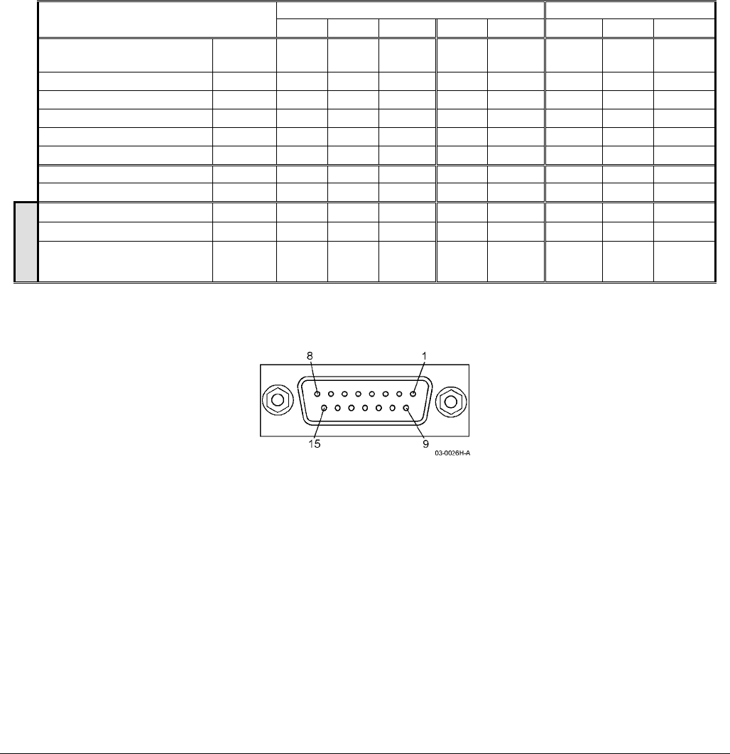
Form-C Alarms Connector
044-05156 Rev C 31
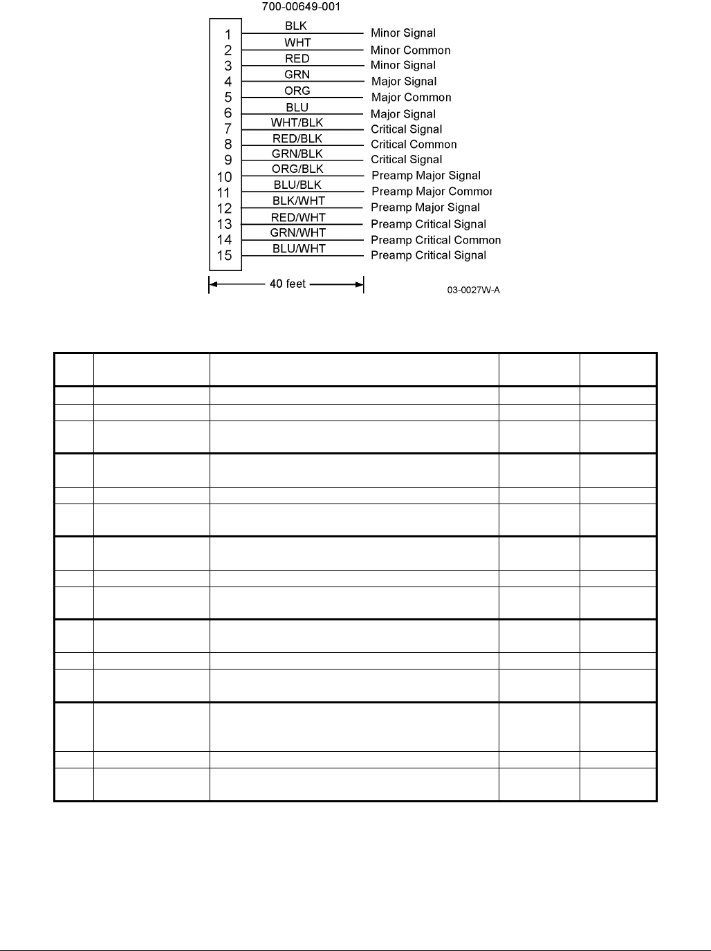
Alarm Cable (optional), P/N 700-00649-001
ALARMS Connector Definition
PIN Alarm Type Function Operating
State
Alarm
State
1 Minor Continuity with common if no fan fault Closed Open
2 Minor Common Common Common
3 Minor Continuity with common if one or more fan
faults on any MCPA Open Closed
4 Major Continuity with common if all installed
MCPAs are active Closed Open
5 Major Common Common Common
6 Major Continuity with common if one or more
MCPAs are disabled Open Closed
7 Critical Continuity with common if one or more
MCPAs are active Closed Open
8 Critical Common Common Common
9 Critical Continuity with common if all installed
MCPAs are disabled Open Closed
10 Preamp Major Continuity with common if external preamp
is functioning correctly Closed Open
11 Preamp Major Common Common Common
12 Preamp Major Continuity with common if external preamp
primary channel faults Open Closed
13 Preamp Critical
Continuity with common if external preamp
primary and redundant channels are
functioning correctly
Closed Open
14 Preamp Critical Common Common Common
15 Preamp Critical
Continuity with common if external preamp
primary and redundant channels are faulted Open Closed
Cable is 24 AWG,
copper wire stripped
and tinned at one end.
Indicated state
is without DC
power applied.
See ALARMS
Connector
Definition table
044-05156 Rev C 32
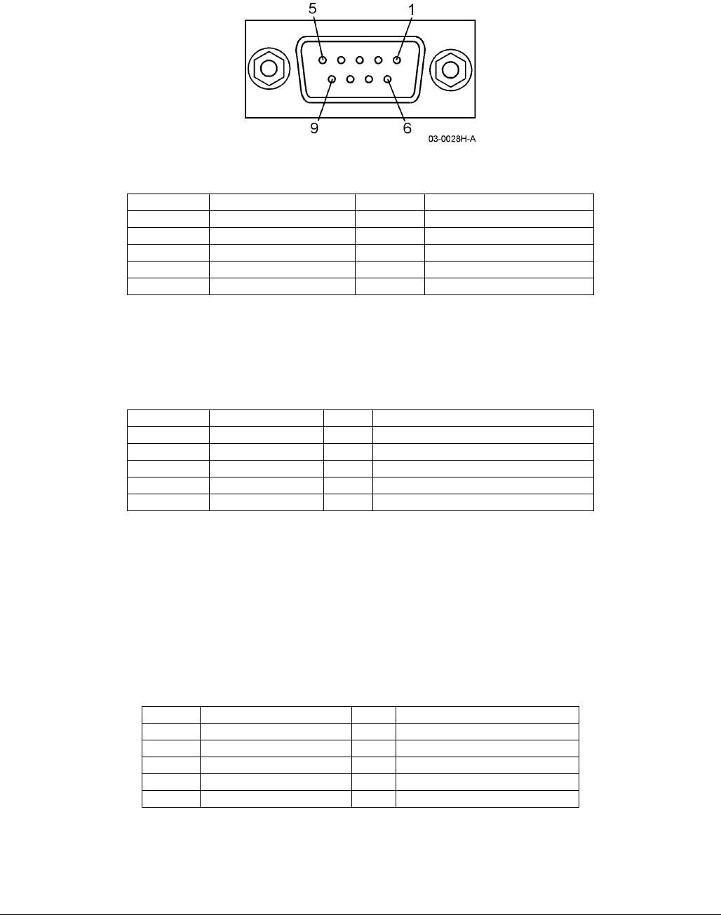
4.6.5.2 RS-485 Connectors (J4, J5)
RS-485 signals are monitored through the RS-485 9-pin female D-sub connector on the rear of the subrack.
DB9 Connector
RS-485 and Preamp Connector Definition
PIN Description PIN Description
1 RS-485 TX data + 6 No Connection
2 RS-485 TX data - 7 No Connection
3 RS-485 RX data + 8 No Connection
4 RS-485 RX data - 9 Ground
5 Ground/Shield
4.6.5.3 Preamp Connector (J6; not used)
Alarm information from the system preamplifiers are monitored through this female 9-pin sub connector located on
the rear of the MCPA subrack. The OPAF-1923-P07C01 does not employ preamplifiers.
Preamplifier Alarm Connector Definitions
PIN Description PIN Description
1 No Connection 6 PA Major +
2 No Connection 7 PA Major -
3 RS-232 TX 8 PA Critical +
4 No Connection 9 PA Critical -
5 Ground/Shield
4.6.5.4 RS-232 Connector
This port is configured for RS-232 serial communications. Refer to the DB9 figure and the RS-232 Connector
Definition (J20) table for pin location and definition. The RS-232 interface is located on the front of the amplifier
subrack. The purpose of this connector is to provide a system interface for upgrading firmware, displaying output
power and system status, and configuration. These tasks are performed using a PC with interface software. The
connector is a type DB-9. The RS-232 port is only enabled if pin 8 is grounded. Grounding pin 8 disables the two
RS-485 host interface ports. Standard 8-bit, 1-stop bit, no parity, 9600 Baud provides the appropriate interface
communication setting.
RS-232 Connector Definition (J20)
PIN Description PIN Description
1 No Connection 6 No Connection
2 RS-232 RX 7 No Connection
3 RS-232 TX 8 Select = 0 (grounded)
4 No Connection 9 No Connection
5 Ground
4.6.6 Pilot Tone Control
Refer to paragraph 4.4.5 for a full description of the amplifier pilot tone. The MCR21929-1-2 subrack can be used to
control the pilot tone frequency of the installed amplifiers. Pilot tone frequency selection is based on the intended
044-05156 Rev C 33
operational band of the amplifiers and must be set during commissioning of the base station, and anytime the
MCR21929-1-2 subrack is replaced.
Setting the pilot tone frequency of the amplifiers requires a laptop interface program. The laptop can be connected
to the MCR21929-1-2’s RS-232 port. The MCR21929-1-2 provides the interface to the amplifiers to set their pilot
frequency and stores this setting in memory. If an amplifier fails, the MCR21929-1-2 programs the pilot frequency of
the replacement amplifier to that of the other installed amplifiers.
4.7 DLNA
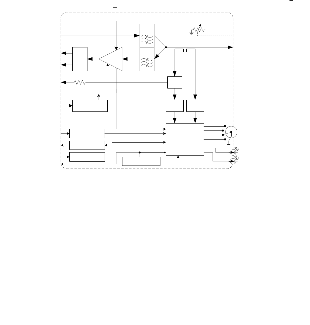
4.7.1 Duplexer Overview
The Duplexer Low Noise Amplifier (DLNA) module provides Bandpass filtering for both the uplink (receive) and
downlink (transmit) paths, as well as gain for the receive path and alarm monitoring for receive gain and VSWR.
The DLNA presents excellent return loss on all ports with 18 dB or better. The coupled ports are accurate to +1.0
dB; the –55 dB sample port is accurate to +2.5 dB
TX
RX
LNA1:2
FWD
-40 dB
REF
-40 dB
1:2
A:D A:D
micro-C
Alarm
Vcc
Gain
Adjust
Regulator
Vcc
Vcc
RS-485 RX
RS-485 TX
RS-485 RX Vcc
Temp Sensor
1
2
3
4
VSWR
S1
Gain
Adjust
Antenna
N-F
TX In
N-F
RX Div
SMA-F
RX Main
SMA-F
TX
Sample
-55 dB
+27 VDC
VSWR Alarm
LNA Alarm
04-0066B-A
45 dB
Gain
DLNA Block Diagram
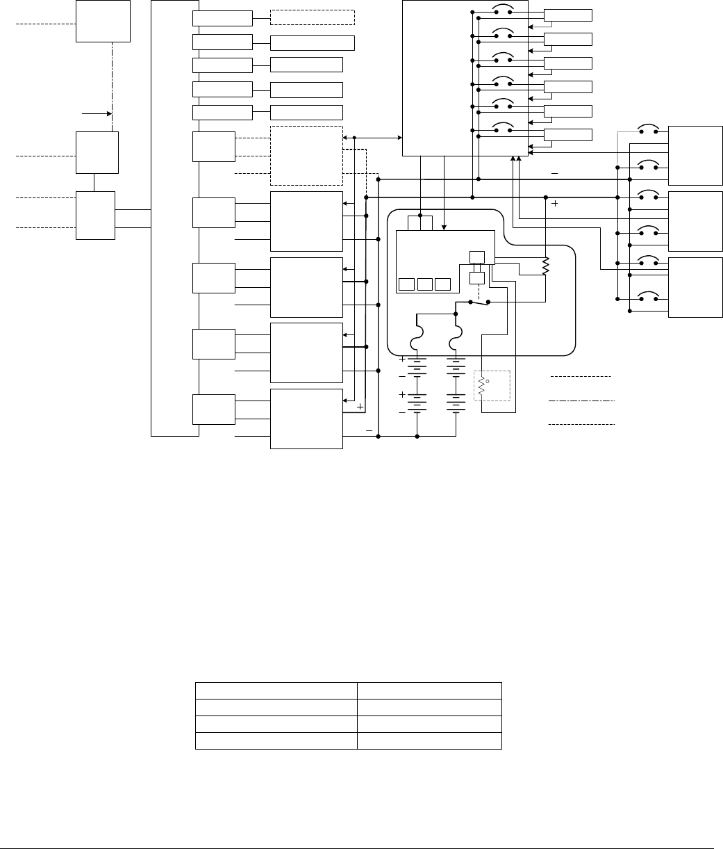
4.7.2 Receive Path Overview
The receive path provides for a variable gain Low Noise Amplifier (LNA) from 43 to 45 dB. The LNA gain is
controlled from a front panel 10-turn potentiometer. The LNA is set to 45 db of gain from the factory. The output of
the LNA is further split into two paths, reducing the receive gain by approximately 3.3 dB, for input to the base
station. The noise figure of the DLNA is typically better than 2 dB at room temperature including all DLNA
components. The main receive path is used for the 8x8 configuration. The diversity receive path is used for the
16x16 configuration.
A microprocessor in the DLNA monitors the current draw of the LNA. If the LNA current draw drops below a
predetermined threshold, an LNA alarm is generated back to the SIM. In addition, a front panel LED is illuminated
when the LNA fails.
044-05156 Rev C 34
DLNA Front Panel
4.7.3 Transmit Path Overview
The transmit path receives amplified RF signals from the MCR21929-1-2 amplifier subrack. The amplified signals
are filtered and duplexed with the receive signals and presented to the antenna port. The transmit filter provides
105 dB of isolation in the receive band between the transmit and antenna ports.
4.7.4 DLNA Alarms
VSWR and LNA alarms for the DLNA are given on the front panel and sent via an alarm bus to the SIM.
Close-up View of DLNA Front Panel
Alarm indications for the DLNA are as follows:
VSWR LED
Green (ON) Normal
Red (ON) Alarm State 1
Yellow (ON) Alarm State 2
Green/Red (OFF) Alarm State 3
Fast Flash Test Mode
LNA LED
Green (ON) Normal
Green (OFF) Loss of Supply voltage
044-05156 Rev C 35
A front panel four-position rotary switch is provided to set the VSWR alarm threshold based on the length of cable
from DLNA output (typically FSJ4 or LDF4) to the antenna foam jumper (typically 1 5/8 Heliax). The switch position
is set with a jeweler’s screwdriver. As a general guide, set the switch as follows:
Alarm Thresholds (in dB; Return Loss)
DLNA
Number
Switch
Position
Design
Tolerance
(dB)
Internal
Cabinet
Cable Loss
External
Cabinet
Cable Loss
Alarm
State 1
Minor
Alarm
State 2
Major
Alarm
State 3
Critical
1 1 0.25 <0.75 6 +2 9.5 +2.5 12 +3
2 2 0.25 >0.75, <1.75 8 +2.25 11.5 +3 14 +3.5
3 3 0.25 >1.75, <2.75 10 +2.5 13.5 +3 16 +4
0
4 Test - - - - -
1 1 0.23 <0.77 6 +2 9.5 +2.5 12 +3
2 2 0.23 >0.77, <1.77 8 +2.25 11.5 +3 14 +3.5
3 3 0.23 >1.77, <2.77 10 +2.5 13.5 +3 16 +4
1
4 Test - - - - -
1 1 0.16 <0.84 6 +2 9.5 +2.5 12 +3
2 2 0.16 >0.84, <1.84 8 +2.25 11.5 +3 14 +3.5
3 3 0.16 >1.84, <2.84 10 +2.5 13.5 +3 16 +4
2
4 Test - - - - -
1 1 0.14 <0.86 6 +2 9.5 +2.5 12 +3
2 2 0.14 >0.86, <1.86 8 +2.25 11.5 +3 14 +3.5
3 3 0.14 >1.86, <2.86 10 +2.5 13.5 +3 16 +4
3
4 Test - - - - -
1 1 0.09 <0.91 6 +2 9.5 +2.5 12 +3
2 2 0.09 >0.91, <1.91 8 +2.25 11.5 +3 14 +3.5
3 3 0.09 >1.91, <2.91 10 +2.5 13.5 +3 16 +4
4
4 Test - - - - -
1 1 0.07 <0.93 6 +2 9.5 +2.5 12 +3
2 2 0.07 >0.93, <1.93 8 +2.25 11.5 +3 14 +3.5
3 3 0.07 >1.93, <2.93 10 +2.5 13.5 +3 16 +4
5
4 Test - - - - -
4.7.5 DLNA Interface
The DLNA employs a DB-15 connector to communicate via the SIM and receive input DC power. Communication is
accomplished using I2C with the BTS signaling.
The SIM knows whether or not all DLNAs are connected by a module detect circuit provided on each DLNA
(ground on pin 9).
J6 DB15 Pin Assignments
PIN Description PIN Description
1 27V 9 Detect
2 27V 10 Temp Out
3 Ground 11 (mfg test use only)
4 Ground 12 (mfg test use only)
5 Write Protect 13 SCL_N (RX)
6 SCL_P (RX) 14 SDA_TX_N
7 SDA_TX_P 15 SDA_RX_N
8 SDA_RX_P
Via I2C, the alarms can be read and an EEPROM can be both read and written too. The SIM however does read
the temp sensor on the DLNA. The DLNA has an RS-232 interface that is only used during test and is not wired out
to the SIM.
044-05156 Rev C 36
The LNA alarm is sensed within the LNA for both low and high current. A single open collector output is read by the
micro-controller and passed on the to I2C interface.
4.8 Power Plant
The power plant incorporates EMI filtering, AC surge suppression, a series of circuit breakers, load sharing
rectifiers, battery backup, DC power monitoring, and a Low Voltage Disconnect transfer switch.
LVD
Monitor
System
Interface
Module
150 A
Main
CB
4 KW
(148 amp)
Rectifier
Line
Line
GND
4 KW
(148 amp)
Rectifier
Line
Line
GND
4 KW
(148 amp)
Rectifier
Line
Line
GND
4 KW
(148 amp)
Rectifier
Line
Line
GND
4 KW
(148 amp)
Rectifier
Line
Line
GND
Alpha
Amplifier
Subrack
Beta
Amplifier
Subrack
Gamma
Amplifier
Subrack
Alarm 1
Alarm 2
Alarm 3
04-0063B-B
DLNA 3
DLNA 2
DLNA 1
DLNA 0
DLNA 4
DLNA 5
30 A
CB
30 A
CB
30 A
CB
30 A
CB
30 A
CB
15 A CB GFCI Outlet
15 A CB AC Relay
20 A CB Surge Pro.
30 A CB Battery Heater
30 A CB Reserved
Line
Line
100 A
100 A
T
EMI
Filter
Line
Line
GND
Bus
Neutral
Bus
GND
Neu
Connect when wired
as Main Panel;
Disconnect when
wired as Sub-Panel
(default)
Customer Supplied
Prewired
Prewired
600A
600A
K1
K1 K2 K3
K4
600A
AC / DC Power Block Diagram
4.8.1 Rectifiers
A series of four 4 KW rectifiers (PN: 930-00018-005) is employed to provide the OPAF power. The rectifiers source
592 amps of combined output DC power at +27 VDC under normal operating conditions. The rectifiers are
designed to operate on 180 to 264 VAC, single phase power, 47 to 63 Hz, and operate at 89% efficiency. They do
not require any minimum load to operate. The rectifier system is modular in design. N+1 redundancy is built into the
system, so a failure in one rectifier does not affect the performance of the base station. Each rectifier provides
performance data and alarms to the LVD controller and the SIM. In addition to the 30 amp circuit breaker installed
in the AC panel, each rectifier is protected by an internal 30 amp 3AG fuse.
The rectifier front panel provides 3 LEDs for quick fault determination
Rectifier LED Definitions
LED Indication
AC Good Green = OK
Temperature OK Green = OK
DC Good Yellow = OK

044-05156 Rev C 37
Rectifier Subrack Pin Assignments
PIN Description PIN Description
1 5 Vbs 9 AC fail
2 5 Vbs rtn 10 V prog
3 Module Detect 11 V1 sense
4 Pgood 12 I monitor
5 On/off 13 Tem OK
6 I share 14 Rtn Sense
7 Mod-Ena 15 No Connection
8 0VP tp
4.8.2 Batteries
Should the AC input power fail for any reason, four 12 Vdc, 105 AH (rated 8-hour capacity) deep discharge Valve-
regulated Lead-Acid batteries provide 24 Vdc power for the entire cabinet. The LVD controller will accommodate
other battery ratings, however, it is factory set for this battery.
The batteries provide a minimum of 12 minutes battery backup time at 25 deg C when presented with the full
cabinet load. The batteries have a wide operating temperature range of –40 to +60 deg. C. The nominal charge
voltage = 2.27-2.30V/Cell or 27Volts @ 25°C with temperature compensation.
nSubtract 3mV/ °C from +25 to +60°C
nAdd 3mV/ °C from +25 to -40°C
Battery Backup Time
No. of G3S-1900-125
Modules
MCPA
Amperes
1 Battery String
(Minutes)
2 Battery Strings
(Minutes)
1 52.8 90 210
2 105.6 37.5 90
3 158.4 20 52
4 211.2 12 37.5
5 264.0 7 26
6 316.8 4 20
Note The charge rate of the batteries is set for C/10 for the batteries delivered with the system. If for any
reason a different type of battery is installed in the system, charge must be changed to avoid
improper charging of the batteries.
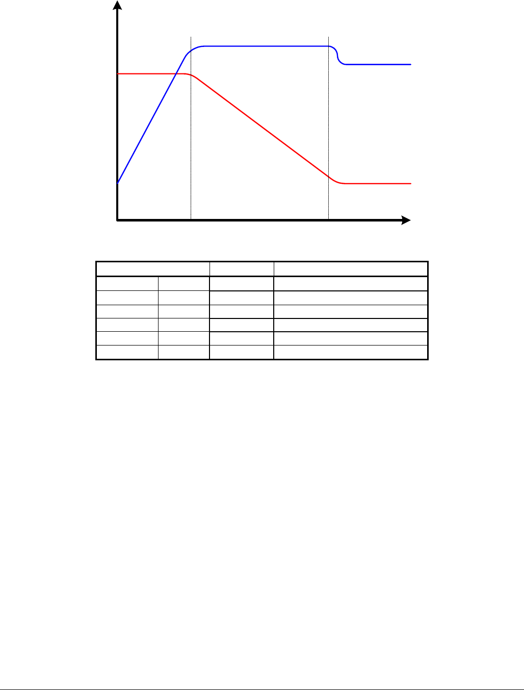
044-05156 Rev C 38
Charger Capacity
Time
Battery Current
Battery Voltage
Constant Current
Stage Absorpation Mode Float Mode
Battery Recharge Cycle from Full Discharge
(1.75 V/Cell) to 100% Charge
Recharge Time 4 x 4KW Modules
G3S-1900-125 MCPA Load Time to 80% Recharge (Hours)
1 MCPA 52.8 0.38
2 MCPA 105.6 0.36
3 MCPA 158.4 0.35
4 MCPA 211.2 0.38
5 MCPA 264 0.38
6 MCPA 316.8 0.42
The batteries meet: UL, NEBS, and EUROBAT requirements and have a 10 year plus classification compliance.
They have also been tested in accordance with BS6290 Part 4. Two 600A fuses (Bussmann PN: TPL-CZ), located
in the LVD, protect the batteries.
4.8.2.1 Battery Heater
The battery heater is a thin, sheet-like element located between metal panels directly beneath the batteries. The
battery heater receives 240 volts AC (400 W) directly from the AC panel circuit breaker through a temperature
sensitive relay. The AC contacts of the relay close when the ambient temperature in the battery compartment drops
below 0 °C (32 °F) allowing the heater to warm the compartment. The heating pad is turned off when the thermostat
reaches 10 °C (50 °F). A separate temperature probe is placed in the battery compartment that is used by the LVD
to adjust the charge voltage, and is independent of the battery heater.
The battery heater generates 400 watts (1367 BTUs) of heat and has a maximum surface temperature of 200 ºC or
392 ºF.
4.8.3 Power Plant Monitoring
A controller card in the LVD monitors the performance of the rectifiers. When each rectifier’s sense line is
connected to the LVD, the rectifier is slaved to the control card for the final output voltage. Therefore, both the
sense line and +27 Vdc bus between the LVD and the rectifier must be connected for the rectifier to supply the
correct voltage to the system. The LVD control module may control up to 6 rectifier modules and adjusts rectifier
output to the recommended battery float voltage for a given temperature.
The LVD controller ensures that the rectifier outputs are balanced and monitors the rectifiers for failures. A
potentiometer located on the front plate of the controller sets the float voltage at 25°C (77°F). The factory preset is
27.6 Vdc. Failures are reported to the SIM.
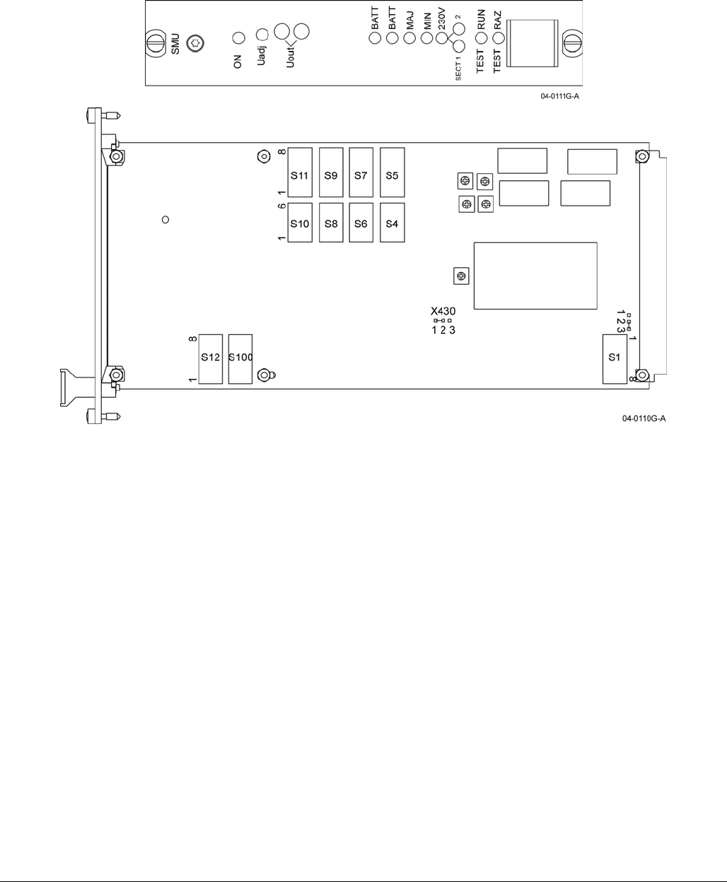
044-05156 Rev C 39
The controller also monitors the battery compartment temperature. The output bus voltage is adapted with
consideration to the temperature changes of the batteries. The compensation slope is user selectable as one of
three values: -36mV/°C (-20mV/°F), –60mV/°C (-33.3mV/°F), and between -10°C (14°F) and 60°C (140°F). The
factory setting is –36mV (-3mV/°C/cell). If the probe is not connected or fails to open, the output voltage falls back
to factory preset and an alarm is generated.
The LVD controller card switch settings are given in the table below.

044-05156 Rev C 40
Switch Pos State Note Switch Pos State Note
1 Off 1 Off
2 Off 2 Off
3 Off 3 Off
4 Off 4 Off
5 Off 5 Off
6 On 6 Off
7 Off 7 Off
S1
8 Off
S7
8 Off
1 On 1
On
2 Off 2 On
3 Off 3 On
4 Off 4 Off
5 Off 5 Off
6 Off 6 Off
7 Off 7 Off
S100
8 Off
S5
8 Off
1 Off 1 Off
2 On 2 Off
3 On 3 Off
4 Off 4 Off
5 On 5
On
6 On
S10
6 On
7 On 1 Off
S12
8 On 2 Off
1 Off 3 Off
2 Off 4 Off
3 Off 5 Off
4 Off
S8
6 Off
5 Off 1 Off
6 Off 2 Off
7 Off 3 Off
S11
8 Off 4 On
1 Off 5 On
2 Off
S6
6 On
3 Off 1 Off
4 Off 2 Off
5 On 3 Off
6 Off 4 Off
7 Off 5 Off
S9
8 Off
S4
6 Off
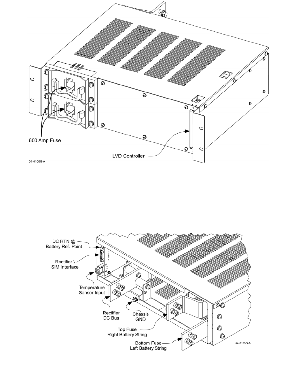
044-05156 Rev C 41
4.8.4 Low Voltage Disconnect (LVD)
Low Voltage Disconnect Module
The purpose of the LVD is to monitor the DC bus to regulate the rectifier(s) output voltage with regard to the
needed operating voltage to the system, and the appropriate charge voltage for the batteries. Should AC power fail,
back-up batteries are installed in the system to provide a relatively short operational period, based on the amplifier
load at the time of failure. When the battery performance declines to a predefined limit (21 Vdc in this system), the
LVD controller disconnects the batteries from the load through a 600 amp transfer switch. Disconnecting the
batteries at this threshold prevents permanent damage to the batteries, thereby extending the battery life. Low
voltage alarms sent to the base station provide sufficient time to do initiate an orderly shutdown of the base station
before power is lost.
LVD Rear Panel Connections
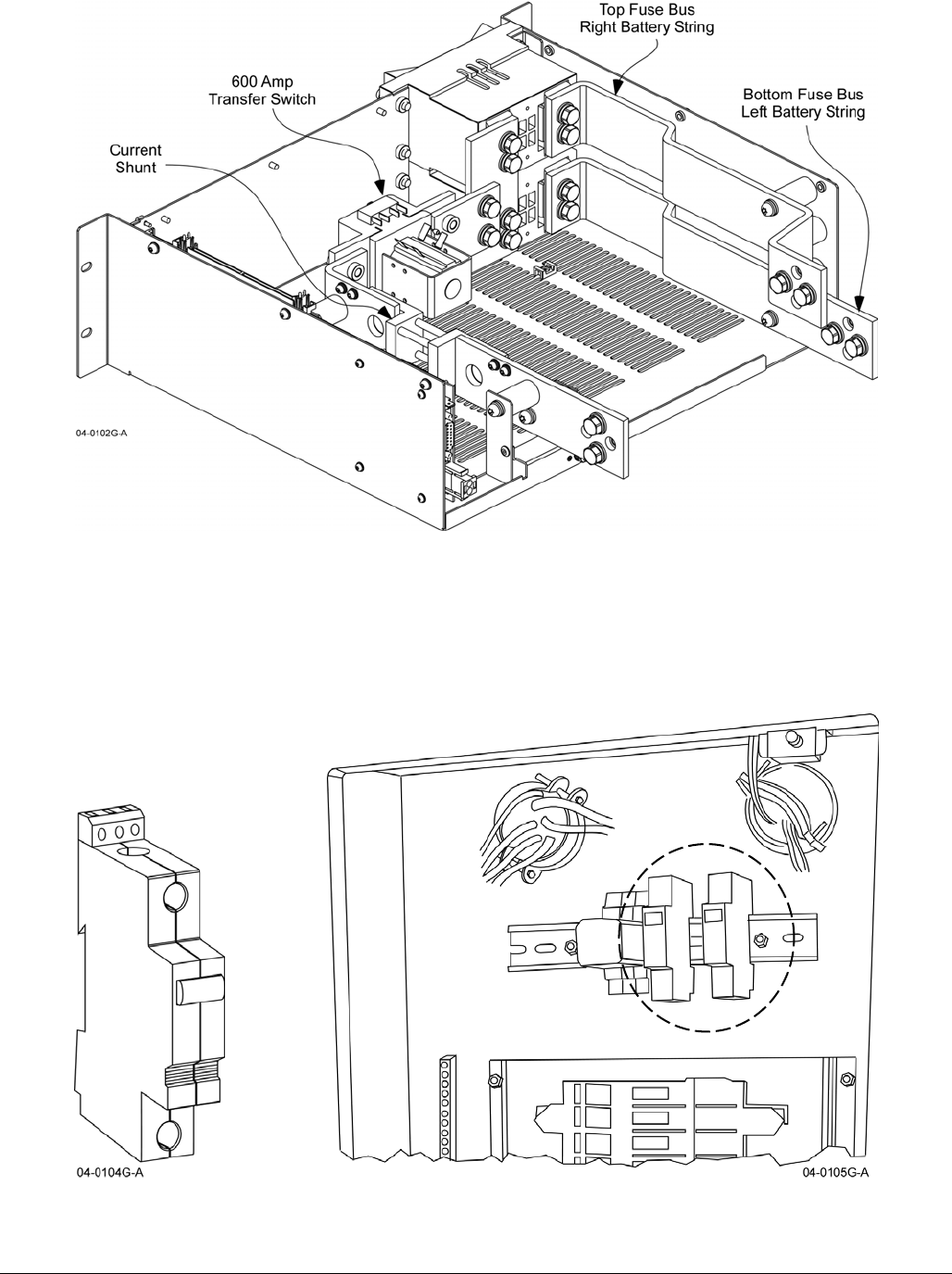
044-05156 Rev C 42
LVD Internal Component Locations
The controller functions of the LVD are described in the Power Plant Monitoring section of this manual.
4.8.5 Lightning Arrestors
Two lightning arrestors located in the AC electrical panel provide added protection to the cabinet when the cabinet
is properly grounded. The lightning arrestors are equipped with push-button trip-resets. The lightning arrestors
characteristics are given in the specifications section of this manual.
Lightning Arrestor Circuit Breaker Panel, Top Portion
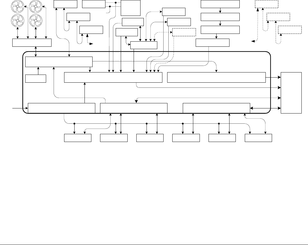
044-05156 Rev C 43
4.9 System Interface Module (SIM)
The SIM monitors the following system attributes and alarms:
Cabinet level alarms (DALI):
Fan Fault
Intrusion
Temperature
AC Fault
AUX
Rectifier level alarms; up to 5 rectifiers (DALI):
Temperature Good
AC Input Good
DC Power Output
Module Detect
MCPA Subrack level alarms (DALI):
Minor (Fan Failure)
Major (Single MCPA Failure in a full subrack)
Critical (All MCPAs Failed in a full subrack)
MCPA level alarms (integrated with the subrack alarms):
Over Power
High Temperature
VSWR
DC Fail
Fan Fail
Loop Fail
Low Power
DLNA level alarms (I2C interface):
LNA fault
VSWR Monitor
Temperature
LVD (DALI):
Transfer Switch
Fuse Blown
DALI 1 DALI 2
I2C Main I2C DiversityCircuit Breakers
Front Door
Rear Door
Battery Door
VAC Door
µCtrl RS-485
+27
VDC
Fan Ctrl
Temp
DLNA 0-5
Temp
MCR 0
MCR 2
MCR 4
MCR 1
MCR 3
MCR 5
AC
Relay
Surge
VAC
LVD
Rect 1
Rect 2 Rect 3
Rect 5Rect 4
DLNA 0 DLNA 1DLNA 2 DLNA 3DLNA 4 DLNA 5
BTS
04-0107B-A
MCR 4
MCR 1
MCR 1, 3, & 5
Only
Seperate Breaker
for each DNLA
System Interface Module
System Interface Module Interconnect & Block Diagram
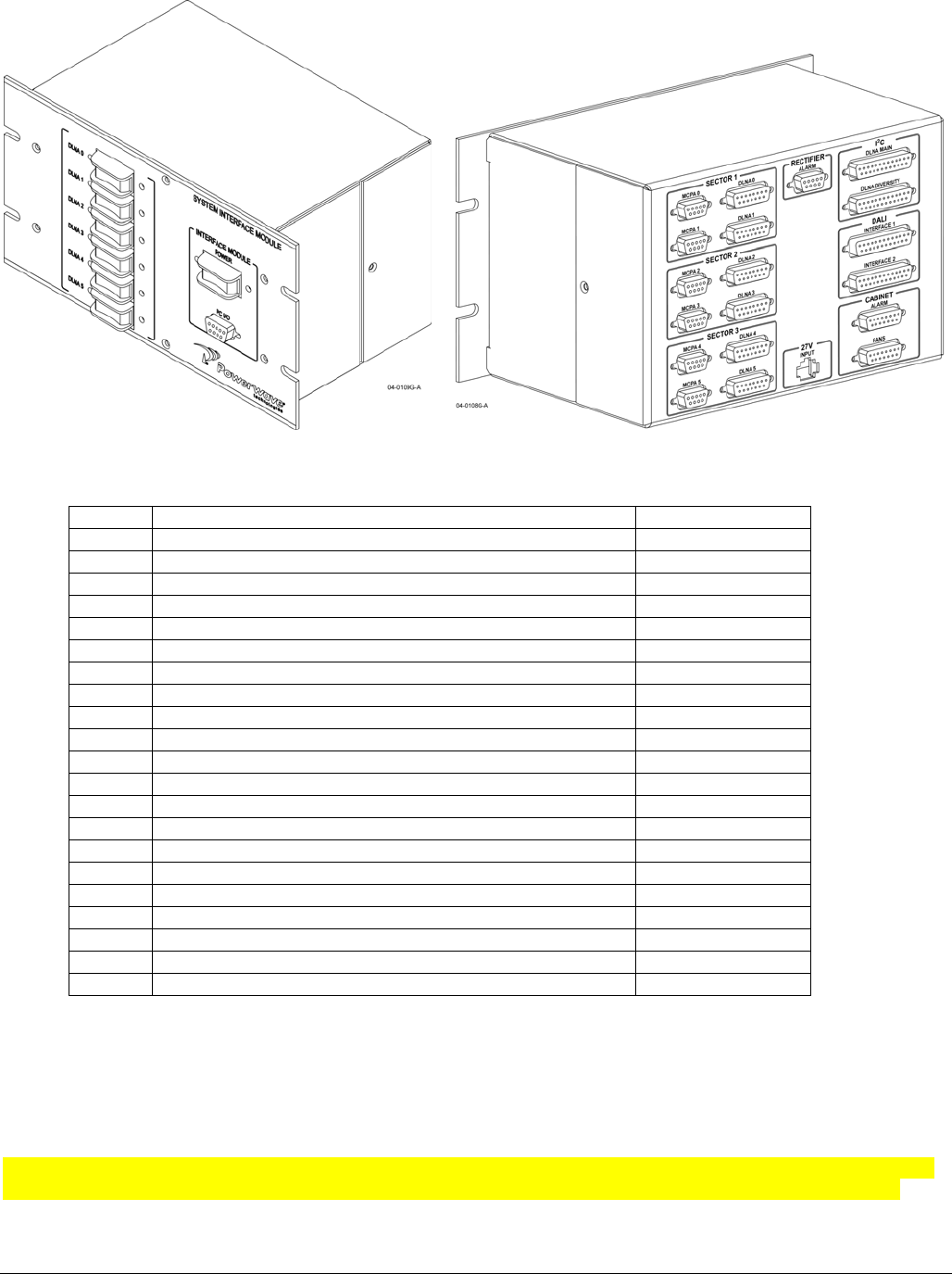
044-05156 Rev C 44
System Interface Module Front and Rear Panels
All input/output connections of the SIM are detailed below:
I/O Description Connector Type
J1 MCPA0 Serial Interface DB-9F
J2 MCPA1 Serial Interface DB-9F
J3 MCPA2 Serial Interface DB-9F
J4 MCPA3 Serial Interface DB-9F
J5 MCPA4 Serial Interface DB-9F
J6 MCPA5 Serial Interface DB-9F
J7 DLNA0 (Main) Interface DB-15F
J8 DLNA1 (Diversity) Interface DB-15F
J9 DLNA2 (Main) Interface DB-15F
J10 DLNA3 (Diversity) Interface DB-15F
J11 DLNA4 (Main) Interface DB-15F
J12 DLNA5 (Diversity) Interface DB-15F
J13 Rectifier Interface DB-9M
J14 DC Input 2X2 Molex
J15 DALI1 BTS Interface DB-25F
J16 DALI2 BTS Interface DB-25F
J17 DLNA Main BTS Interface DB-25F
J18 DLNA Diversity BTS Interface DB-25F
J19 Cabinet – Intrusion and AC Fault Interface DB-15F
J20 Cabinet – Fan Interface DB-15F
J21 PC RS232 Interface DB-9F
4.9.1 Amplifier Alarms - MCPA Serial Interface (J1 – J6)
The MCPA Serial Interface is accomplished via a DB9 Female connector on J1. The SIM communicates with each
amplifier subrack in the cabinet via the host RS-485 interface on the MCPA subrack. RS-485 signals are daisy
chained from the first subrack to the next, and so on, until the buss is terminated. The SIM is internally terminated,
as are each of the amplifier subracks, to prevent loading down the RS-485 buss.
TBD alternate configuration: The MCPA Serial Interface is accomplished via six identical DB9 Female connectors.
The SIM communicates with each amplifier subrack in the cabinet via the host RS-485 interface on the MCPA

044-05156 Rev C 45
subrack. The SIM is internally terminated, as are each of the amplifier subracks, to prevent loading down the RS-
485 buss.
Pin # Description
1 RS-485 TX data +
2 RS-485 TX data -
3 RS-485 RX data +
4 RS-485 RX data -
5 No Connection
6 No Connection
7 No Connection
8 No Connection
9 No Connection
Descriptions TX and
RX are in reference to
the MCPA subrack.
TX refers to data in to
the SIM.
RX refers to data out
from the SIM.
Amplifier alarms are reported to the SIM via the amplifier subrack RS-485 bus. The amplifier subracks are daisy-
chained on the RS-485 bus, and the alarm bus is cabled from the subrack rear panel to the front panel subrack
interface panel. Each subrack has a unique address. The subrack address is set via front panel dip switches.
Refer to Amplifier Monitoring in the MCR21929-1-2 Amplifier Subrack section of this manual for available alarms.
4.9.2 DLNA Alarms - DLNA Interfaces (J7 – J12)
The DLNA interface is accomplished with six DB15 Female connectors. Each connection is unique and requires
coordination with the DLNAs within the cabinet. Each connector provides DC power to the DLNA, differential I2C
BTS pass-through, and analog temperature signals.
DC power provides the DLNA with +27±1.0 Vdc via a 5A maximum circuit breaker on four contacts (2-source, 2-
return). The circuit breaker also functions as the power switch to the DLNA.
The differential I2C interface utilizes 6 contacts. These signals are passed-through the SIM to the BTS interface. A
module detect signal is also passed through. No processing is provided or required.
A single analog voltage signal (pin 10) represents the temperature of the DLNA module. The voltage potential is
with respect to the DC return. The temperature conversion factor is: 0°C = 500mV +10mV/°C.
PIN Description PIN Description
1 DC Source 9 Module Detect
2 DC Source 10 Temperature Signal
3 DC Return 11 No Connection
4 DC Return 12 No Connection
5 No Connection 13 SCL-
6 SCL+ 14 SDA_TX-
7 SDA_TX+ 15 SDA_RX-
8 SDA_RX+
4.9.3 Power Plant Alarms - Rectifier Interface (J13)
The Rectifier interface is accomplished through a single DB9 Male connector. This interface includes up to six
individual rectifier faults. The faults signals are open collector. The signal impedances are defined as:
Low impedance signifies normal operation
High impedance signifies a fault

044-05156 Rev C 46
The open collector circuit has a 10mA limitation. The interface also includes two auxiliary TTL signals. One is an
input and the other an output. The auxiliary output signal is a 74HC14 inverter output. The auxiliary signals have no
function at this time.
RECT6 signal represents the alarm status of the LVD controller.
PIN Description PIN Description
1 GND 6 Rectifier Fault 5
2 Rectifier Fault 1 7 Rectifier Fault 6 (LVD)
3 Rectifier Fault 2 8 Auxiliary TTL Input
4 Rectifier Fault 3 9 Auxiliary TTL Output
5 Rectifier Fault 4
4.9.4 Cabinet Alarms
4.9.4.1 Cabinet – Intrusion / AC Fault Interface (J19)
A DB15 Female connector provides the Cabinet intrusion and AC fault interface. The intrusion inputs are contact
closures from all of cabinet doors: front, rear, battery, and AC service. All Common contacts are tied to the system
ground. The Normally Closed contacts are pulled-up and passed to the micro-controller. A logic high signal signifies
an intrusion via an open door.
The AC power fault passes through to the DALI interface Common contact with reference to the BTS COMMON1.
An open contact signifies an AC fault. The AC fault signal is not processed.
PIN Description PIN Description
1 Ground 9 AC Door Common Contact
2 Front Door Normally Closed Contact 10 AC Alarm Normally Closed Contact
3 Front Door Common Contact 11 AC Alarm Common Contact
4 Rear Door Normally Closed Contact 12 No Connection
5 Rear Door Common Contact 13 No Connection
6 Battery Door Normally Closed Contact 14 No Connection
7 Battery Door Common Contact 15 No Connection
8 AC Door Normally Closed Contact
4.9.4.2 Cabinet Fan Control and Interface (J20)
Each of the cabinet fans has a sense signal with a 50% duty cycle square wave. The frequency of the square wave
signal is directly proportionate to the RPM of the fan. The speed of the fan is dependant on the applied control
voltage. The rotational speed of the fan is dependent on the applied DC voltage to the control input of the fan. The
control function is supported by a micro-controller.
The fan control ports will be forced to 0% PWM if the front door is sensed open. The fan status will latch to the
current state and all fault times will be halted and saved. Upon the sensed door closure the fan sense routine will
continue where it left off.
The temperature information is derived from:
o The DLNA temperature analog input.
o The MCPA serial interface.
o The SIM internal temperature analog input.
The highest temperature measurement among these devices determines the fan setting. All four-fan control ports
function identically with each other. The PWM outputs do not increment or decrement > 1 step per minute.
If the +27V input is < 24V, the temperature thresholds increase by +10°C. If the voltage is less than 24V the battery
back-up system is assumed the primary DC source and the system will operate at an accelerated temperature to
reduce the current draw of the cabinet fans in an attempt to extend battery life.
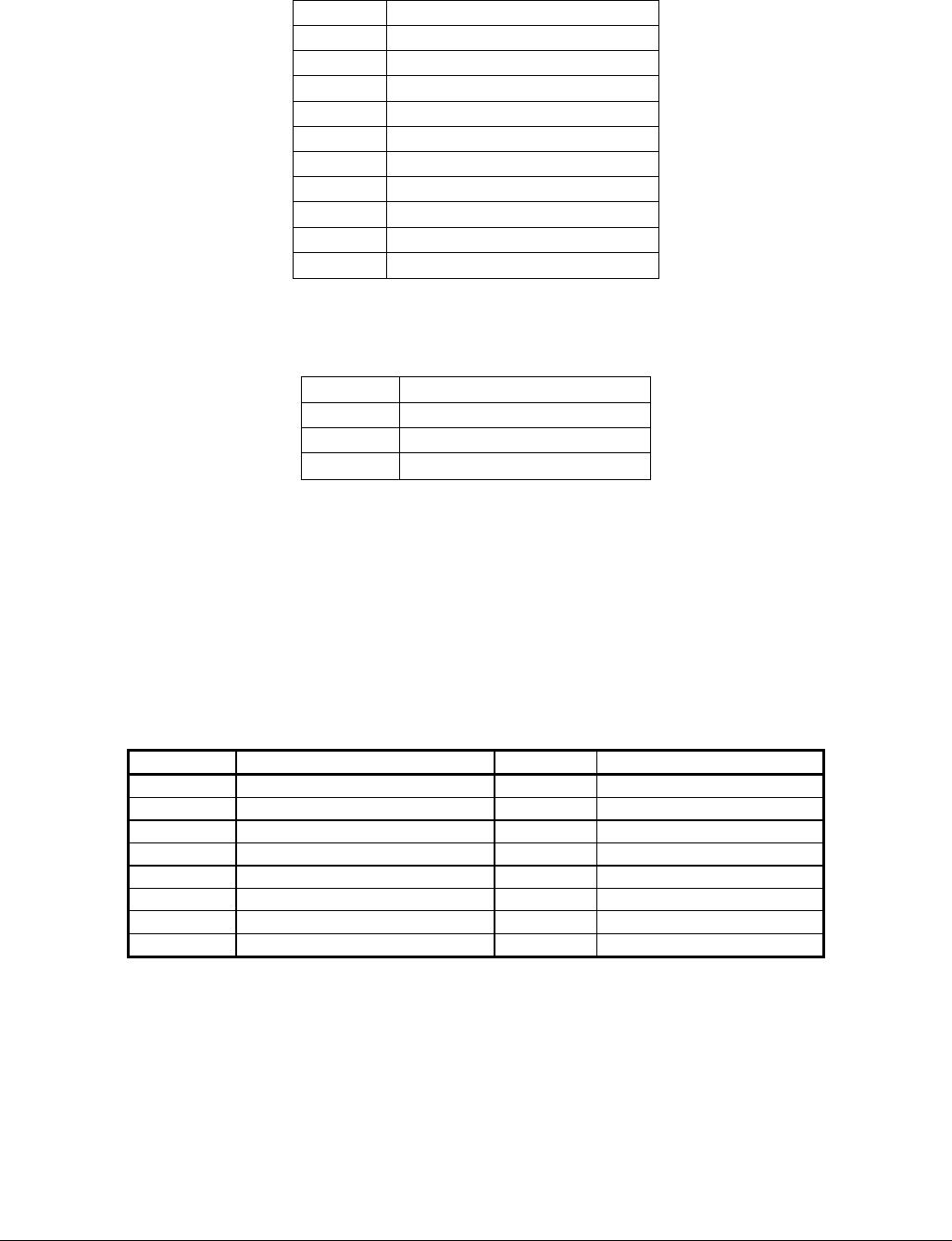
044-05156 Rev C 47
PWM VS. Temperature
PWM (%) Maximum Temperature
0 +41°C or less
15 +42°C
25 +43°C
35 +44°C
45 +45°C
55 +46°C
65 +47°C
75 +48°C
85 +49°C
100 +50°C or greater
There are three fan fault frequency thresholds related to speed control.
Fan Fault Thresholds
PWM (%) Fan Fault Threshold
100 - 50 40Hz
49 - 20 15Hz
< 20 10Hz
Each fan sense input is measured. If the fan frequency(s) is below the threshold (for the operating mode) for a
continuous period of 1-minute a fan fault is reported to the DALI interface. Any change in fan status is reported to
the BTS in real-time via the I2C interface. The fan fault on the DALI is cleared when all of the fan frequencies
maintain above threshold performance for a period of 30 seconds. Alarm monitoring will halt if the fan control is
0%PWM. When this occurs, the current alarm status latches.
The cabinet fan interface is a DB15 Female connector. The interface provides fan monitor inputs, and fan control /
status outputs.
The fan control circuitry provides a 0 to 10Vdc signal to adjust the fan speed.
Pin # Description Pin # Description
1 Ground 9 Fan 0 Sense
2 Fan1 Sense 10 Fan 2 Sense
3 Fan3 Sense 11 I2C Serial I/O Data
4 I2C Serial I/O Clock 12 Ground
5 Ground 13 No Connection
6 No Connection 14 Fan 3 Speed Control
7 Fan 2 Speed Control 15 Fan 1 Speed Control
8 Fan 0 Speed Control
4.9.4.3 RS-232 Interface (J21)
The front panel of the SIM provides a RS-232 serial communication port. The RS-232 port provides for upgrading
firmware, and displaying system status and configuration. These tasks are performed via PC and interface
software.
Upgrading firmware
Display all DALI alarms
Display all DLNA, MCPA and SIM temperatures in °C
044-05156 Rev C 48
Display the fan control voltage (0-10)
Display the fan speed in Hz
Pin # Description Pin # Description
1 No Connection 6 No Connection
2 RS-232 TX 7 No Connection
3 RS-232 RX 8 No Connection
4 No Connection 9 No Connection
5 Ground
4.9.5 DALI Interfaces (J15 & J16)
The two DALI interfaces are accomplished via two DB25 Female connectors. The DALI interface reports all of the
cabinet alarms, excluding the DLNA alarms, to the BTS. The interface is made through Form-B contact with a
reference provided by the BTS (COMMON1 or COMMON2).
DALI PIN Signal Description DALI PIN Signal Description
1 1 DALI0 MCPA0_ALARM1 2 1 DALI0 MCPA1_ ALARM1
1 2 DALI1 MCPA0_ ALARM2 2 2 DALI1 MCPA1_ ALARM2
1 3 DALI2 MCPA0_ ALARM3 2 3 DALI2 MCPA1_ ALARM3
1 4 DALI3 MCPA2_ ALARM1 2 4 DALI3 MCPA3_ ALARM1
1 5 GND Ground (Common1) 2 5 GND Ground (Common2)
1 6 DALI4 MCPA2_ ALARM2 2 6 DALI4 MCPA3_ ALARM2
1 7 DALI5 MCPA2_ ALARM3 2 7 DALI5 MCPA3_ ALARM3
1 8 DALI6 MCPA4_ ALARM1 2 8 DALI6 MCPA5_ ALARM1
1 9 DALI7 MCPA4_ ALARM2 2 9 DALI7 MCPA5_ ALARM2
1 10 GND Ground (Common1) 2 10 GND Ground (Common2)
1 11 DALI8 MCPA4_ ALARM3 2 11 DALI8 MCPA5_ ALARM3
1 12 DALI9 RECT1 2 12 DALI9 OPEN
1 13 DALI10 RECT2 2 13 DALI10 OPEN
1 14 DALI11 RECT3 2 14 DALI11 OPEN
1 15 GND Ground (Common1) 2 15 GND Ground (Common2)
1 16 DALI12 FAN ALARM 2 16 DALI12 OPEN
1 17 DALI13 INTRUSION 2 17 DALI13 OPEN
1 18 DALI14 HI_TEMP 2 18 DALI14 OPEN
1 19 DALI15 LO_TEMP 2 19 DALI15 OPEN
1 20 GND Ground (Common1) 2 20 GND Ground (Common2)
1 21 DALI16 RECT4 2 21 DALI16 OPEN
1 22 DALI17 RECT5 2 22 DALI17 OPEN
1 23 DALI18 RECT6 2 23 DALI18 OPEN
1 24 DALI19 AC ALARM 2 24 DALI19 OPEN
1 25 GND Ground (Common1) 2 25 GND Ground (Common2)
1 26 NC - 2 26 NC -

044-05156 Rev C 49
4.9.6 I2C Interfaces - DLNA Main (J17) / Diversity (J18)
The two DLNA I2C BTS interfaces are accomplished via two DB25 Female connectors. The DLNA I2C interface is
passes-through all of the DLNAs status and module detect signals to the BTS. The I2C interfaces are full duplex
and differential (6 I/Os).
I2C Pin Signal Description I2C Pin Signal Description
1 1 SDA_RX_P DLNA_0 2 1 SDA_RX_P DLNA_1
1 2 SDA_RX_N DLNA_0 2 2 SDA_RX_N DLNA_1
1 3 SDA_TX_P DLNA_0 2 3 SDA_TX_P DLNA_1
1 4 SDA_TX_N DLNA_0 2 4 SDA_TX_N DLNA_1
1 5 SCL_P DLNA_0 2 5 SCL_P DLNA_1
1 6 SCL_N DLNA_0 2 6 SCL_N DLNA_1
1 7 DETECT DLNA_0 2 7 DETECT DLNA_1
1 8 NC DLNA_0 2 8 NC DLNA_1
1 9 GND DLNA_0 2 9 GND DLNA_1
1 10 SDA_RX_P DLNA_2 2 10 SDA_RX_P DLNA_3
1 11 SDA_RX_N DLNA_2 2 11 SDA_RX_N DLNA_3
1 12 SDA_TX_P DLNA_2 2 12 SDA_TX_P DLNA_3
1 13 SDA_TX_N DLNA_2 2 13 SDA_TX_N DLNA_3
1 14 SCL_P DLNA_2 2 14 SCL_P DLNA_3
1 15 SCL_N DLNA_2 2 15 SCL_N DLNA_3
1 16 DETECT DLNA_2 2 16 DETECT DLNA_3
1 17 NC DLNA_2 2 17 NC DLNA_3
1 18 GND DLNA_2 2 18 GND DLNA_3
1 19 SDA_RX_P DLNA_4 2 19 SDA_RX_P DLNA_5
1 20 SDA_RX_N DLNA_4 2 20 SDA_RX_N DLNA_5
1 21 SDA_TX_P DLNA_4 2 21 SDA_TX_P DLNA_5
1 22 SDA_TX_N DLNA_4 2 22 SDA_TX_N DLNA_5
1 23 SCL_P DLNA_4 2 23 SCL_P DLNA_5
1 24 SCL_N DLNA_4 2 24 SCL_N DLNA_5
1 25 DETECT DLNA_4 2 25 DETECT DLNA_5
1 26 NC DLNA_4 2 26 NC DLNA_5

044-05156 Rev C 50
5. Specifications
Note This Powerwave product is designed to operate within the Normal Operating (typical
operating) ranges or conditions specified in this document. Operation of this equipment
beyond the specified ranges in this document may cause (1) spurious emissions that violate
regulatory rules; (2) the equipment to be automatically removed from service when maximum
thresholds are exceeded; or (3) the equipment to not perform in accordance with its
specifications. It is the Operator's responsibility to ensure this equipment is properly installed
and operated within Powerwave operating specifications to obtain proper performance from
the equipment and to comply with regulatory requirements.
Cabinet Specifications
Material Aluminum alloy 0.12 inch (3.05 mm) thick
Finish Non-corrosive plating
Alarms Intrusion for all doors
Fans 1200 CFM min; 65 dBA max with doors shut; turn-off when door is opened
Electrical entry External AC entry box with grounding bus bar; AC power filtering
Grounding Single point grounding; Interior grounding buss; all doors and cover plates
provide good electrical ground.
Door Locks Front and Rear doors provide 3 point locking mechanisms
Door and access plate seals UL-157 compliant
Mounting Template Mylar plate; provided
Lock Tool Thin-wall 7/16 inch nut driver
Cable Access Plate Tool Keyed T-27 Torx driver
Lifting Bosses Qty 4; 6000 lbs (2721 Kg) max weight supported with proper strapping
Wind Speed Up to 150 MPH (241.4 Km/H)
Solar Loading Top (100 % Area): 754 W/m2
Front and one side (100 % Area): 754 W/m2
Compliance Telcordia GR-487-CORE; Bellcore GR-63-CORE
Dimensions:
Footprint
Overall, Doors Closed
Overall, Doors Open
34 W x 34 D inches (863.6 W x 863.6 D mm)
42.5 W x 79.5 H x 39.4 D inches (1079.5 W x 2019.3 H x 1000.8 D mm)
59 W x 79.5 H x 105 D inches (1498.6 W x 2019.3 H x 2667.0 D mm)
Weight
Empty
Without Amplifiers, Rectifiers
and Batteries
Fully Loaded
400 lbs (181.5 Kg)
614.5 lbs (278.7 Kg)
1345 lbs (610 Kg)

044-05156 Rev C 51
G3S-1900-125 Multicarrier PCS Amplifier Functional Specifications
Frequency Range 1930-1990 MHz
Total Maximum Input Power -4 dBm
Total Output Power 125 W typical (1 Module)
Intermodulation Distortion and In-Band
Spurious: -63 dBc (Min) @ +26 to +28 Vdc @ 125 Watts
RF Gain at 1930 MHz 60 dB
Gain Flatness: ±0.5 dB @ 27 Vdc ±1 Vdc
Gain Variation Over Temperature: ±0.5 dB from 24 to 30 Vdc
Output Protection: Mismatch Protected
Input Port Return Loss: -16 dB (Min)
Out of Band Spurious: Better than -60 dBc, +24 Vdc to +28 Vdc
Duty Cycle: Continuous
DC Input Power: +27 Vdc ± 1 Vdc, 52 amps Typical, 60 Amps Max @ 125 Watts;
Operational +21.0 Vdc to 30 Vdc
Operating Temperature: 0 ºC. to +50 ºC.
Storage Temperature: -40 ºC. to +85 ºC.
Operating Humidity: 5 % - 95 % Relative Humidity (Noncondensing)
Storage Humidity: 5 % - 95 % Relative Humidity (Noncondensing)
RF Input / Output Connector Radial BMA Female Blind Mate Connector
Status / Alarm / Control / DC Input Connectors: 21-Pin D-Subminiature Combo Connector
Dimensions (Including handles, rear fans): 5.22 H x 16.97 W x 20.44 D inches
(132.59 H x 431.04 W x 519.18 D mm)
Weight 52 lbs (23.59 Kg)

044-05156 Rev C 52
MCR21929-1-2 Specifications
Frequency Range 1930-1990 MHz (see Pilot Tone Control section)
Power Output / Max Input
w/125W modules
109 W (50.37 dBm) / 1.87 dBm (1 Module)
218 W (53.38 dBm) / 1.88 dBm (2 Modules)
Duty Cycle Continuous
RF Gain – Standard (±0.50 dB) 48.5 dB 1 Module
51.5 dB 2 Modules
RF Gain – Constant (±0.50 dB) 48.0 dB
RF Gain Adjust 0 to 10 dB Standard operating mode
0 to 3 dB Constant Gain operation mode
0 dB when preamps are employed
Gain Variation with Voltage / Freq. ± 0.5 dB @ 26 to 28 VDC
Gain Variation over Temperature ±0.5 dB
Input Port Return Loss 13 dB (min)
Subrack Noise Figure 34.0 dB 1 Module
31.0 dB 2 Modules
+ Gain Adjust Attenuation value (0-10 dB)
DC Input Voltage Range 21 to 30 VDC (26 to 28 VDC for rated operation)
RF Power Derating for DC Input
Voltage
28V ≤ V < 30V 0.5 dB
26V ≤ V < 28V 0.0 dB Normal operating voltage
24V ≤ V < 26V 0.5 dB
22V ≤ V < 24V 1.0 dB
21V ≤ V < 22V 1.5 dB
DC Input Current per Subrack 104 Amps Typical, 120 Amps Max (2 Modules) @ 27 ±1 VDC
Alarms (Subrack) Minor – Fan Fail
Major – One or more MCPAs Failed
Critical – All MCPAs Failed
Alarm Indication Form C Contacts, LEDs & RS-485
Operating Temperature Range 0 °C to + 50 °C, Ambient
Storage Temperature -40 °C to + 85 °C
Operating Humidity, Normal 0% - 80% RH (Noncondensing)
Storage Humidity 0% - 100% RH (Noncondensing)
Connectors
DC
RF Input
RF Output
Alarm Outputs (Form-C)
RS-485 (2), Preamp (1), and
RS-232 (1)
Strip-n-Poke (2 to 10 AWG)
SMA Female
7/16 DIN Female
15-Pin D-Subminiature Female
9-Pin D-Subminiature Female
Controls
Subrack Address
Subrack Operating Mode
Indicators APC (RED)
Dimensions: 19 W x 12.17 H x 25 D inches (19 W x 12.17 H x 25 D mm)
Weight: 38 lbs. Empty; 142 lbs. Fully Loaded (17.24 Empty; 64.41 Kg Loaded)

044-05156 Rev C 53
DLNA Specifications
Electrical Characteristics
Parameter Limit Unit Remarks
Transmit (TX) Path specific
Frequency Range 1930-1990 MHz
Insertion Loss 1.2 dB Max Over entire Pass band
Loss variation over temperature 0.4 dB Any given frequency
In-Band Ripple (J1: TX to J2: Antenna Port) 0.7 dB Max Over Temp
Input Power, Average (J1: TX) 250 W Continuous
Peak Instantaneous Power Handling 5 kW PIP @ an altitude of 4000 m
Rejection (J1: TX to J2: Antenna Port) 85 dB Min over DC – 1850 MHz
Rejection (J1: TX to J2: Antenna Port) 105 dB Min over 1850-1900 MHz
Rejection (J1: TX to J2: Antenna Port) 97 dB Min over 1900-1910 MHz
Rejection (J1: TX to J2: Antenna Port) 45 dB Min over 2015 – 4000 MHz
Rejection (J1: TX to J2: Antenna Port) 35 dB Min over 4000 – 12750 MHz
Inter modulation Distortion (IMD3) in TX Band
(J1: TX to J2: Antenna Port) -80 dBc
2 tones @100W (+50dBm) / Tone at
(J1: TX)
-59 dB DC – 1910 MHz Isolation (J1: TX to J3:RX_01) or
(J1:TX to J4: RX_02) -34 dB 1930 – 12750 MHz
Receive (RX) Path Specific (Antenna port to LNA output port)
Frequency Range 1850-1910 MHz
Gain (J2: Antenna to J3: RX_01) or
(J2: Antenna to J4: RX_02) 45.0+/- 0.5 dB at Fc=1880 MHz & Room temp)
-121 to –23 dBm Max GMSK average power
Dynamic power range: -121 to –26 dBm Max EDGE average power
Input IP3 -8.0 dBm Min. (Added filter loss)
Input P1dB -16.0 dBm Min. (Added filter loss)
Variable attenuation, voltage controlled +0.0 /- 2.0 dB via front panel potentiometer
Gain variation, over temperature + 1.0 dB Full Band
Gain flatness, over specified frequency range 1.7 dB Filter ripple, Filter + LNA
2.0 dB Max at Room Temp.
Noise Figure 2.5 dB Max Over Temp.
Rejection (J2: Antenna to J3: RX_01) or
(J2: Antenna to J4: RX_02) 90 dBc Min. over DC to 1720 MHz
Rejection (J2: Antenna to J3: RX_01) or
(J2: Antenna to J4: RX_02) 40 dBc Min. over 1720 to 1820 MHz
Rejection (J2: Antenna to J3: RX_01) or
(J2: Antenna to J4: RX_02) 25 dBc Min. over 1820 to 1830 MHz
Rejection (J2: Antenna to J3: RX_01) or
(J2: Antenna to J4: RX_02) 0 dBc 1830 to 1850 MHz
Rejection (J2: Antenna to J3: RX_01) or
(J2: Antenna to J4: RX_02) 0 dBc Reference = 1850 to 1910 MHz
Rejection (J2: Antenna to J3: RX_01) or
(J2: Antenna to J4: RX_02) 0 dBc 1910 to 1930 MHz
Rejection (J2: Antenna to J3: RX_01) or
(J2: Antenna to J4: RX_02) 90 dBc Min. over 1930 to 2050 MHz
Rejection (J2: Antenna to J3: RX_01) or
(J2: Antenna to J4: RX_02) 70 dBc Min. over 2050 to 4000 MHz
Rejection (J2: Antenna to J3: RX_01) or
(J2: Antenna to J4: RX_02) 30 dBc Min. over 4000 to 12750 MHz
Isolation (J3: RX_01) to (J4: RX_02) 15 dB Over the specified frequency range
Gain balance 0.5 dB Between (J3: RX_01) & (J4: RX_02)

044-05156 Rev C 54
Electrical Characteristics
Parameter Limit Unit Remarks
Inter modulation Distortion (IMD7) RX Band
(J3: RX_01) to (J4: RX_02) -110 dBc
Measured @ 1870 MHz., 2 tones
@100W (+50dBm)/Tone at J2:
Antenna
General Specification
Max Input RF -10.0 dBm RMS power with no damage to
DLNA
-18 dB (J1: TX) 50 ohm matched.
Input Return Loss -18 dB (J2: Antenna) 50 ohm matched
Supply Voltage Range +20 to +30 Vdc
Supply Voltage Range 27+ 0.5 Vdc Nominal
DC Current 2 A Max.
VSWR 1.5:1 Max; Source and Load
Sample Port J5
Frequency Range 1930~1990 MHz
Loss (J1: TX port to J5: Sample Port) -55±2.5 dB N Nominal
Flatness (J1: TX port to J5: Sample Port) 2.0 dB Max
Output Return Loss (J5: Sample) -18 dB Max (50 ohm matched)
Mechanical
Connector - TX port N-type F 1
Connector - RX Ports SMA F 2
Connector - Antenna Port N-type F 1
Connector - Sample Port SMA F 1
Connector - DC power & I/O DB15 1
Switch Rotary 4
position 1
LED 2
Dimensions 16.12 L x 9.50 W x 1.75 H inches
(409.12 L x 241.3 W x 44.45 H mm)
Weight 9 KG (19.8 lbs)
Common Environmental characteristics
Value
Characteristic Test Conditions
Min Max
Unit
Transportation Shock IEC 68-2-27
Transportation Bounce IEC 68-2-55
Operating Altitude(Note 2) - 152 4000 Meter AMSL
Operating Temperature Range - 20 +85 ºC
Storage Temperature Range - 40 +85 ºC
Operating Humidity Non-condensing 0 95 %RH
Notes:
1. Maximum ratings represent the limits beyond which damage to the device may result. Continuous operation
of the device at the maximum rating limit is prohibited.
2. Max op temp may be derated by 2 degrees C/1000 ft above 2154 meters.

044-05156 Rev C 55
System Interface Module Specifications
Operating Voltage +27 +0.5 VDC nominal; 20 min to 30 VDC max
Current 5 amps typical; 7.2 amps max
Operating Temperature -40 to +80 °C
Storage Temperature -40 to +80 °C
Humidity 5 to 95% RH, non-condensing @ 50 °C
Interface Signals Form-B
Open-Collector TTL, 5 V pull-up, 5 mA max
Open-Collector Fan Sense, 5 V pull-up, 1 mA max
Fan Control, 0 to 10 VDC typical, 12 VDC max
RS-232
RS-485
Output Voltage DLNA use, 21 to 27 VDC, 5 amp circuit breaker protection, 6 outputs
Dimensions 9.5 W x 5.4 D x 5.22 H inches (241.3 W x 136.91 D x 132.56 H mm)
Weight 3 lbs (1.4 Kg)
148-Amp Rectifier Model 930-00018-005 Specifications
Input Voltage 180 / 264 Vac, 47 / 63 Hz, Single phase
Input Current 25.5 Amps @ full load @180 Vac
Power Factor 0.99 typical
Inrush Current 50 Amps maximum
Harmonic Distortion <5% total @ full load; <3% @ each harmonic
Efficiency 89% typical @ 230 Vac
Hold-Up Time >20 ms @ low line
Output Voltage Range +20.0 to +29.0 Vdc (set to +27.0 for Powerwave)
Line Regulation 0.5% using remote sense (5% on standby voltage)
Load Regulation 0.5% using remote sense (5% on standby voltage)
Output Ripple & Noise < 1% P-P
Transient Response 3 % max deviation. 0.50 ms recovery time for a 25% load change
Start-Up Time 2 Seconds
Hold-Up time >20 ms @ low line
Overshoot/Undershoot 1% at turn on/off
Temperature Coefficient 0.02% per ºC
Remote On/Off Logic 1(TTL high) or open enables unit (on), Logic 0 (TTL low) or short shuts unit
down (Off)
Power Fail Signal Signal goes low (TTL low) 2 ms before loss of output regulation
Current Limit Protection 110-140% V1, 5VSB <2.5 amps automatic recovery
Over Voltage Protection 29.5 to 30.5 V. Reset by cycling input power
Over Temperature
Protection
Automatic shutdown with auto recovery. Thermal shutdown point @ 95 ºC
MTBF 300,000 hours per Belcore standard
Output Power Good TTL high = power good, TTL low = output out of limits
LED Indicators DC good = green LED; temperature OK = green LED; AC good = amber LED
Operating Temperature 0 to 50 ºC @ rated output power. Supply derates linearly from 50 ºC to 65 ºC @
2.2% per ºC
Cooling Self contained ball bearing fan
Shock and Vibration Per MIL STD-810F, NEBS compliant to GR 63 Core
EMI/EMC Meets EN61000-3-2, -3 CISPR22 and FCC Part 15 Class A, Bellcore GR1089-Core
Safety Approvals Meets UL1950, CSA 22.2 #650, TUV EN60950 and CE Mark
Dimensions 5.0 W x 16.14 D x 5.0 H inches (127.0 W x 409.96 D x 127.0 H mm)
Weight 13.5 lbs (6.12 Kg)
Specifications as provided by Cherokee International, Document Number 97MS2101M, Revision A, Aug 1, 2003

044-05156 Rev C 56
LVD Specifications
Electrical Specifications
DC bus connection Specification Comments
Nominal voltage
User adjustable values
Factory set
26.5V, 26.75V, 27V, 27.25V
27V
At 25°C adjustable by dip switches
located on the controller board when
programming signal is connected
rectifier programming pins
Voltage range 20Vdc to 30Vdc
Bus voltage monitoring
Pre alarm user value range
Pre alarm Factory set
Battery disconnect range
Factory set
23Vdc or 25Vdc
25Vdc
21V or 22V
21Vdc
Set by dip switches on the controller
Rated bus current 600A Nominal
Battery connections
Number of connections 2
Battery type (AH) 40; 60; 100; 200; 300 VRLA; Capacity set by dip switches
Temperature compensation
Temperature range
Slope user adjustable values
Factory set
-10°C to 60°C /(14°F to 140°F)
0; -36; -48; -60 mV/K
-36mV/K
Based on temperature probe when
enabled
Set by dip switches on the controller
Battery protection
Fuse rating ranges
Factory set
70A to 600A
600A
Single blade fuse on each battery
branch with auxiliary contacts
Battery Disconnect
User settable voltage
values
Factory set
Reconnect
21V or 22V
21Vdc
24V
Set by dip switches on the controller
Battery charge current
limitation; Factory set
C/10
Environmental
Operating temperature range -25°C to 70°C (-13°F to 158°F)
Max. humidity 80% non condensing
Safety Meets EN 60950; All
components are UL approved
when mounted in an enclosed 19
inch frame
Mechanical
Dimensions: Width x Depth x
Height
19 W x 14.2 L x 5.25 H inches
(482.6 W x 360 L x 133 H mm)
Weight 15 lbs (6.8 Kg)
Front panel Fuse, Controller Maintenance access
Connections
DC Bus Screw connection Back of the module
Battery connection Screw connection Back of the module
Signals connection Sub-D 15p female Back of the module
Grounding M6 stud Back of the module
Battery Heater Specification
Operating Voltage 240 VAC
Power 400 W
Thermostat Set Points Close at 0 ºC (32 ºF); Open at 10 ºC (50 ºF); tolerance + 3.3 ºC (+ 6 ºF)
Maximum Surface Temperature 200 ºC (392 ºF)
Dimensions 20.5 L x 20.5 W x 0.030 H inches (521 L x 521 W x 0.76 H mm)
044-05156 Rev C 57
12 VDC 105 AH Battery Model 920-00337-003 Specifications
Cells / Volts 6 Cells / 12 Volts (DC)
Terminal Type Threaded Copper Insert, ¼ inch
Capacity @ 77 ºF (25 ºC) 105 AH (8 hrs) to 1.75 Volts (DC) per cell
Operating Temperature -40 ºC to +60 ºC (-40 ºF to +140 ºF)
Charging Voltage / Current 2.27 to 2.30 Volts (DC) per cell, constant voltage at a maximum current of C/4 amps
Temperature
Compensation
nSubtract 3mV/ °C/cell above +25 °C or 1.7 mV/°F/cell above 77 °F
nAdd 3mV/ °C below +25 °C or 1.7 mV/°F/cell below 77 °F
Storage time from a fully
charged condition 6 months at 25 °C / 77 °F; for each 9 °C / 15 °F rise, reduce storage time by half
Self discharge rate < 2% per month at 25 °C / 77 °F
AC ripple from charging
source 1.5% peak to peak of float
Overall dimensions Inches: 21.96 L x 4.86 W x 8.93 H; mm: 558 L x123 W x 227 H
Weight 90 lbs / 41 kgs
Specifications as provided by Power Battery Company, Inc., Document Number 1606-1-0310
I2R SA120-40 AC Lightning Arrestor Specifications
Item UOM Specification
Tested to IEC 61643-1
Arrester class acc. to IEC 61643-1 II
Nominal voltage (50/60 Hz) UN 120V
Max. continuous operating voltage UC 170V
Max. discharge current at wave shape Imax (8/20) Imax 40kA
Nominal discharge current at wave shape In(8/20) UP 20kA
Voltage protection level at In I
n <850V
Response Time ta <25ns
Recommended back-up fuse 160AgL/gG
Short-circuit withstand capability IP 60kAef
Recommended cross-section of connecting
conductors θ 25mm2 (solid)
16mm2 (flexible)
Operation temperature range -40 to +80 ºC
Protection type acc. to CSN EN 60529 IP 20
Mounting on DIN rail 35mm
Housing’s material FRNC-UL94VO Flame Rating
Weight 3.2 oz (90g)
Potential free signal contact electrical strength against surrounding circuits 3750Vef
electrical strength against network circuit 3750Vef
insulation resistance 2x10⁷W
max. switching current ~0,5A
max. switching voltage ~250V
Specifications as provided by Transtector, Inc., Document Number 1458-009_Rev0 (R8-11/04/02)