Q MAC Electronics HF90 HF-90 User Manual Technical manual
Q-MAC Electronics Pty Ltd HF-90 Technical manual
Contents
- 1. User guide
- 2. Technical manual
- 3. Technical Manual
- 4. User Guide
Technical manual

- 1 -
No part of this manual may be copied, transcribed, translated or reproduced in any manner or form
whatsoever, for commercial purposes, without obtaining prior written permission from Q-MAC
Electronics Pty Ltd. However, limited copying is permitted for private use providing authorship is
acknowledged.
© Copyright Q-MAC Electronics Pty Ltd, 2003.
142 Hasler Road
Osborne Park, WA 6017
PO Box 1334
Osborne Park Business Centre, WA 6916
AUSTRALIA
Australia: Phone 08 - 9242 2900, Fax 08 - 9242 3900
International: Phone +618 - 92242 2900, Fax +618 - 9242 3900
First Edition
Print date: August 1996
Second Edition
Print date: February 1997
Third Edition
Print date: October 2000
Author: Rod Macduff
Literature Reference Number: TECH02C.PUB
Part Number: QM1021
Additional Technical Support:
Note that additional technical support is available to Q-MAC Dealers under the “Dealer Support”
section of the Q-MAC website: www.qmac.com. This site incorporates Technical Bulletins issued by
Q-MAC, plus Technical Notes and Instructions in relation to specific products.

- 2 -
TABLE OF CONTENTS
Section 1 Warnings & advice
..............................................................................................4
Section 2 Introduction
........................................................................................................... 5
Section 3 Product specification
........................................................................................ 6
Section 4 Mechanical assembly
.........................................................................................7
Section 5 Functional overview
...........................................................................................8
Section 6 Block diagrams
Front panel.................................................................................................................10
Microprocessor..........................................................................................................11
Receiver/exciter.........................................................................................................12
Synthesizers...............................................................................................................13
Power amp & switching P.S.U. .................................................................................14
Section 7 Circuit description
7.1 Front panel PCB ...............................................................................................15
7.2 RXMP PCB ....................................................................................................16
7.3 PASW PCB ....................................................................................................21
Section 8 Tables & diagrams
Table 1. HF-90 micro port allocations ................................................................24
Diagram 1. Serial link chain ....................................................................................25
Table 2.
Diagram 2. Superhet. mixing scheme ......................................................................26
Diagram 3. HF-90 Rx gain distribution ...................................................................26
Table 3. HF-90 Tx low pass filters......................................................................27
Table 4. HF-90 connector pinouts.......................................................................28
Diagram 4. Connector positions...............................................................................30
Section 9 Maintenance
9.1 Disassembly & assembly..................................................................................31
9.2 Replacement of Microprocessor.......................................................................32
9.3 Radio alignment................................................................................................33
Section 10 Fault finding
10.1 No tools fault finding......................................................................................36
Section 11 Diagnostic test sequence
11.1 Receiver test sequence....................................................................................39
11.2 Transmitter test sequence ...............................................................................43

- 3 -
Section 12 Test point overlays
12.1 RXMP test point voltages...............................................................................45
HF-90 P.A. board alignment - position reference......................................................46
Section 13 Software overview
13.1 Program description........................................................................................47
13.2 Routine description (not frequency hopping).................................................48
13.3 Software releases............................................................................................50
Section 14 Hints & tips
14.1 Device removal...............................................................................................51
14.2 Servicing warnings .........................................................................................52
14.3 Servicing case histories...................................................................................53
Section 15 Parts List
15.1 Front panel PCB parts list (ISSUE N) ............................................................60
15.2 RXMP PCB parts list (ISSUE V)...................................................................61
15.3 PASW PCB parts list (ISSUE Q) ...................................................................67
Section 16 PCB overlays
Front panel top overlay - issue N (designators).........................................................72
Front panel top overlay - issue N (component values)..............................................73
RXMP top overlay - issue V (designators)................................................................74
RXMP top overlay - issue V (component values).....................................................75
PASW top overlay - issue Q (designators)................................................................76
PASW top overlay - issue Q (component values) .....................................................77
Section 17 Schematic diagrams
HF-90 display (90000)...............................................................................................79
HF-90 I.F. strip, micro section & synth (90003).......................................................80
HF-90 P.A. & power supply (90002) ........................................................................81
Section 18 External connectors
.........................................................................................82
Section 19 Device pinouts & codes
Device pinouts...........................................................................................................84
19.1 SMD capacitor codes......................................................................................85
- 4 -
1. On no account should the unit be connected directly to 110volt or 240volt AC mains
power. Serious damage or personal injury may result.
2. An approved 12volt or 24volt power supply or battery should be used. The supply
should be capable of sourcing peak currents up to 10ampere. Failure to comply with
this rating will result in severe distortion on transmissions. Please note that some
power supplies labeled as 10ampere peak are not adequate as the voltage collapses
towards the peaks.
3. Use only the approved power cable for installation. Use of thinner conductors or
extensions will result in severe distortion on transmissions.
4. The system performance is generally only as good as the antenna and ground system
will allow. If unbalanced antennas are being used eg. whips, end-fed broadbands etc,
then it is vital to obtain a good low impedance ground connection either to a vehicle
body, a moist patch of ground or a metal fence with rust removed at the point of
connection.
5. The HF-90 is extremely small. When transmitting, the heatsink and extrusion may get
very hot. Under some circumstances it may be possible to get burned by touching the
heatsink. The radio has been designed and tested to cope with elevated temperatures.
However the user should endeavour to allow free circulation of air around the radio.
6. In order to achieve the high output power, an internal power convertor is used to
supply +55volt to the final amplifier on transmit. The energy stored by this supply is
quite high (2.2joules) and it is wise to WAIT FOR A FULL MINUTE after
transmitting prior to doing any service work on the PASW printed circuit board.
7. Radio Frequency Field Exposure: The HF-90 Packages generate high radio frequency
fields. Their antennas are marked with a safe working distance in accordance with
required Standards. This should be observed.
8. This device complies with Part 90 of the FCC Rules. Operation is subject to the
condition that this device does not cause harmful interference.
1. WARNINGS & ADVICE
!
!

- 5 -
2. INTRODUCTION
The HF-90 Compact Transceiver breaks new ground in the following areas:
Size: The volume of the transceiver is approximately one litre. This is less than a tenth of
comparable products. On initial inspection it is often mistaken for a VHF/UHF set.
Weight: At 1 kilogram, the HF-90 is a quarter of the weight of products with a similar
specification.
Ease of use: The HF-90 has quite deliberately been kept simple so that persons unfamiliar
with HF communications may immediately pick it up and use it.
Low cost: The transceiver has been designed using state of the art SMD technology.
Components from cellular telephony, satellite television, and personal computers have been
used wherever possible to keep the cost at a minimum. Also, wherever possible,
functionality has been implemented in software rather than hardware.
Ruggedness: Use of a heavily ribbed aluminium extrusion confers great strength to the
HF-90. Stainless steel handles protect all front panel controls. A ribbed rear heatsink
protects the rear connectors.
Reliability: Use of SMD technology and the delegation of functionality to software has led
to simplicity of design which translates to high reliability. Unreliable parts such as
potentiometers and wiring looms are avoided. All internal connectors have gold to gold
mating surfaces.
Serviceability: The HF-90 was designed with serviceability as a top priority. The radio
consists of three PCBs, all of which plug together. Only four screws need be removed to
access the main PCBs. These PCBs plug together as a ‘sandwich’ with all the essential
components and nodes easily probeable while the radio is operating, without the use of
extenders. All power transistors are easily accessed and use single screw fixing.
Minimised inventory: The design of the HF-90 was implemented with the minimum
number of different types of components. Thus spares inventory is reduced.
Versatility: The high performance and small size allows the HF-90 to be used in portable,
mobile or fixed configurations. The wide power supply range (12 to 24volt) makes it
particularly attractive in multi-role applications.
Receiver performance: Excellent receive sensitivity is combined with a large dynamic
range through the use of four GaAs FETs in the front end mixer.
Transmitter performance: A very high power to weight ratio and extreme RF ruggedness
is obtained through the use of 500volt MOS FETs in the power amplifier.
Selcall performance: A sophisticated digital signal processing algorithm is capable of
extracting very weak calls in the presence of noise. Successful decodes at down to -132dBm
have been observed.

- 6 -
3. PRODUCT SPECIFICATION
Specifications are subject to change without notice
General
Frequency range: 2 ! 30MHz
Modes of operation: USB, LSB (J3E)
CW (optional)
Hopping (optional)
AM (Rx only), FSK
Number of channels: 255
Channel resolution: 100Hz
Supply voltage: 12 ! 24V DC nominal
Power consumption:
- Transmit: 2A! 10A
(subject to pre-set power
output)
- Receive: 310mA
Frequency stability: ± 1.5ppm
Antenna impedance: 50Ω
Antenna connector: BNC
Handsets: Speaker microphone
DTMF microphone
& telephone handset
Selcall system: Based on CCIR 493-4
(Australian Standard)
Programming: IBM PC 4800,8,1,N
BITE: Micro, Rx, Tx tests
Environmental
Operating temperature: -30ºC ! 60ºC
Storage temperature: -30ºC ! 80ºC
Humidity: 95% non-condensing
Environmental rating: IP54
Physical characteristics
Dimensions (mm): 112(W) x 47(H) x 220(D)
Weight: 1kg (HF-90 only)
Construction: All metal extruded sleeve
with front panel and
heatsink
Finish: Black anodized aluminium
Transmitter
Power output: 50Watt PEP
Duty cycle: Normal speech or data
(with fan option)
Unwanted sideband: Better than -45dB
Carrier suppression: Better than -50dB
Harmonic suppression: Better than –60dB
Spurious emissions: Better than –60dB
Noise suppression: Better than -35dB
Distortion: Less than 5% @ 70% PEP
Audio response: 270Hz ! 2800Hz
Microphone: Electret insert
Tune: >20W radiated @ +1000Hz
Load protection: ALC
Receiver
Sensitivity: 0.25µV for 10dB S+N/N
Selectivity: 2.3 kHz @ -6dB
6kHz @ -60dB
Image rejection: Better than -50dB
Intermodulation: Better than -70dB
3rd order intercept: +20dBm (GaAs FET
mixer)
Blocking: Better than -70dB
Spurious response: Better than -60dB
IF rejection: Better than -60dB
Intermediate freq’s: 83.16MHz, 455kHz
AGC: Less than 3dB
from 3µV ! 1V
Clarifier range: ± 250Hz
Audio response: 270Hz ! 2800Hz
Audio output: 2Watt
Audio load impedance: 8Ω
Audio distortion: Less than 5% @ 1W

- 7 -
Radio construction
The radio shell comprises a 2.5mm aluminium front plate complete with black stainless steel
handles, a 160mm long key-ribbed sleeve extrusion and a 10-fin extruded rear heatsink. This
provides a simple and strong housing for the radio. Four M3x12 screws are used to secure
both front and rear panels. The display PCB is secured to the metal front-plate by the fixing
nuts of three front panel parts. This allows for simple removal. The two main PCBs pug into
each other as a ‘sandwich’, and the whole assembly slides into the extruded sleeve on
keyways. The rear heatsink is part of the PASW board assembly. Rubber gaskets on the
front and rear mating surfaces give some water resistance.
Front panel
The front panel allows manual control of all the radio functions. This is achieved by six
elastomer keys, an incremental shaft encoder (volume) and a toggle switch for power
activation. A high efficiency 6-digit 7-segment LED display indicates the channel number
on receive and frequency on transmit. An 8-pole microphone socket provides all the external
interface requirements for microphones, headphones, DTMF keypad, and computer interface.
The front panel can be removed by undoing the four screws on the front of the radio and
pulling gently on the handles. It can be further disassembled by simply undoing the two hex
grub screws on the volume knob and unscrewing the volume, on/off switch and microphone
socket nuts. The elastomer keys and fibreglass key separator should be left in the keyholes.
The gold keypads are placed on a small sub-board above the display PCB. Six pins hold this
small keypad in place.
RXMP board
This board has no direct connections to the outside world. It mates both mechanically and
electrically with the PASW board via four 10-way connectors. It also mates via two of the
10-way connectors with the display PCB. There is one unused 10-way pin field for test use.
When mated with the PASW board it slides into the extruded sleeve on keyways.
PASW board
The PASW board incorporates the rear heatsink extrusion as part of its assembly. The
heatsink contains the BNC antenna connector and the 4-pole power receptacle. The heatsink
is attached to the PCB by virtue of the heavy connections to the power receptacle and the 18
power transistor leads. The PASW board mates with the RXMP board via four 10-way
connectors but has no connection to the display PCB.
4. MECHANICAL ASSEMBLY

- 8 -
Front panel
Refer to the block diagram (FRONT PANEL) in Section 6 of this manual.
The only electronic parts of significance on the display PCB belong to the display register
and multiplexor. All other parts merely route signals from the keys, microphone socket,
volume encoder etc to the main two PCBs via a pair of 10-way connectors.
RXMP PCB
This board incorporates three distinct functional blocks, the Microprocessor, Receiver/
Exciter and Synthesizer.
Microprocessor
Refer to the block diagram (MICROPROCESSOR) in Section 6 of this manual.
This section contains the 8-bit microcontroller along with its address latch, battery backed
RAM, data memory and glue logic. For simplicity, communication with peripheral devices
is via a serial 3-wire bus. This bus sends data to the display, volume DAC, transmit low pass
filters and power control. A separate data line feeds the synthesizer. Computer I/O and
Selcall data in, also share the same serial ports. The keypad is read via a 5-wire matrix and
the volume encoder has a 2-line quadrature input plus interrupt. A DTMF decoder handles
tones from the microphone and utilises a memory mapped interface.
Receiver/Exciter
Refer to the block diagram (RECEIVER/EXCITER) in Section 6 of this manual.
The receiver/exciter section is configured as a double superhet with first IF at 83.160MHz
and second IF at 455kHz. The same circuit is used on receive and transmit apart from the
second IF processor. Relays re-route the signal on transmit through the first IF. The other
circuit elements are bi-directional. LO1 and LO2 are synthesizer derived. The carrier
insertion oscillator at 453.6kHz or 456.4kHz is counted down from the LSB or USB crystal.
Synthesizer
Refer to the block diagram (SYNTHESIZER) in Section 6 of this manual.
The first local oscillator uses a high level push-pull circuit. It covers a 30MHz span and is
controlled by one half of the frequency synthesizer running at a high comparison frequency
to obtain low phase noise. The second local oscillator is a simple single ended unit covering
a 20kHz span, controlled by the other half of the frequency synthesizer. The Selcall decoder
uses a PLL and data slicer to demodulate the FSK signal.
PASW PCB
Refer to the block diagram (POWER AMP & SWITCHING PSU) in Section 6 of this manual.
The PASW board contains the main power supplies and the transmitter power train. A
shielded +5volt switching power supply provides power for most of the RX and logic and a
+10volt linear supply is also provided. On transmit a +50volt switching power supply is
active. The transmit power train comprises two RF Op-Amps, the first of which is ALC
controlled, then a driver stage and final amplifier, both of which use MOS FETs. One out of
six harmonic filters is selected by a darlington driver.
5. FUNCTIONAL OVERVIEW

- 9 -
6. BLOCK DIAGRAMS
Please refer to the following pages for block diagrams .....

- 10 -
REFER BLOCK DIAGRAM
“HF-90 RADIO BLOCK DIAGRAM - FRONT PANEL”
IN FILE NAMED “HF90BFP.xxx”

- 11 -
REFER BLOCK DIAGRAM
“HF-90 RADIO BLOCK DIAGRAM - MICROPROCESSOR”
IN FILE NAMED “HF90BMCP.xxx”

- 12 -
REFER BLOCK DIAGRAM
“HF-90 RADIO BLOCK DIAGRAM RECEIVER / EXCITER”
IN FILE NAMED “HF90BRXE.xxx”

- 13 -
REFER BLOCK DIAGRAM
“HF-90 RADIO BLOCK DIAGRAM - SYNTHESIZERS”
IN FILE NAMED “QMAPAPS.xxx”

- 14 -
REFER BLOCK DIAGRAM
“HF-90 RADIO BLOCK DIAGRAM POWER
AMP & SWITCHING P.S.U.”
IN FILE NAMED “HF90BPAP.xxx”

- 15 -
7.1 Front panel PCB
Refer to the schematic diagram (HF-90 DISPLAY 90000) in Section 17 of this manual.
The front panel PCB contains a 6-digit 7-segment LED display, 6-button keypad matrix, on/
off switch, volume control and microphone socket. It measures 35mm x 95mm and contains
eight integrated circuits.
Display data is contained within a 6-byte serial shift register (U1 - U6) and the display is
refreshed at one sixth of the 7kHz clock rate by the multiplex counter (U8 & U25).
The display is updated from the microprocessor via a 3-wire serial interface (TOC, SCK &
DIS). A fourth line DSIRO allows the microprocessor to check for serial link integrity.
The 7-segment display sections (U18 - U23) are extremely compact and efficient resulting in
excellent readability and endurance.
An incremental shaft encoder (VR1) controls the volume level on the Standard and
Advanced Model HF-90 and allows a flexible user interface for possible future options. It
gives 24 detents (clicks) per revolution.
The computer programming interface utilises D1 and Q2 to achieve compatibility with IBM
PC Clone RS232C ports, operating at 4800N81 (4800 baud, no parity, eight data, one stop).
A simple auxiliary PCB contains the 5-line, 6-button keypad matrix. TR and BR (top and
bottom row) carry negative going key scan pulses at 250Hz repetition rate. RCL, MCL and
LCL (right, middle and bottom column) are inputs allowing the key presses to be read by the
microprocessor.
The microphone socket allows use of an unbalanced electret microphone, telephone style
handset with PTT, a DTMF keypad and an RS232C programming link.
A single pole on/off switch activates the power relay on the PASW PCB (power amplifier
and switch mode power supply PCB), by switch closure to ground.
7. CIRCUIT DESCRIPTION
- 16 -
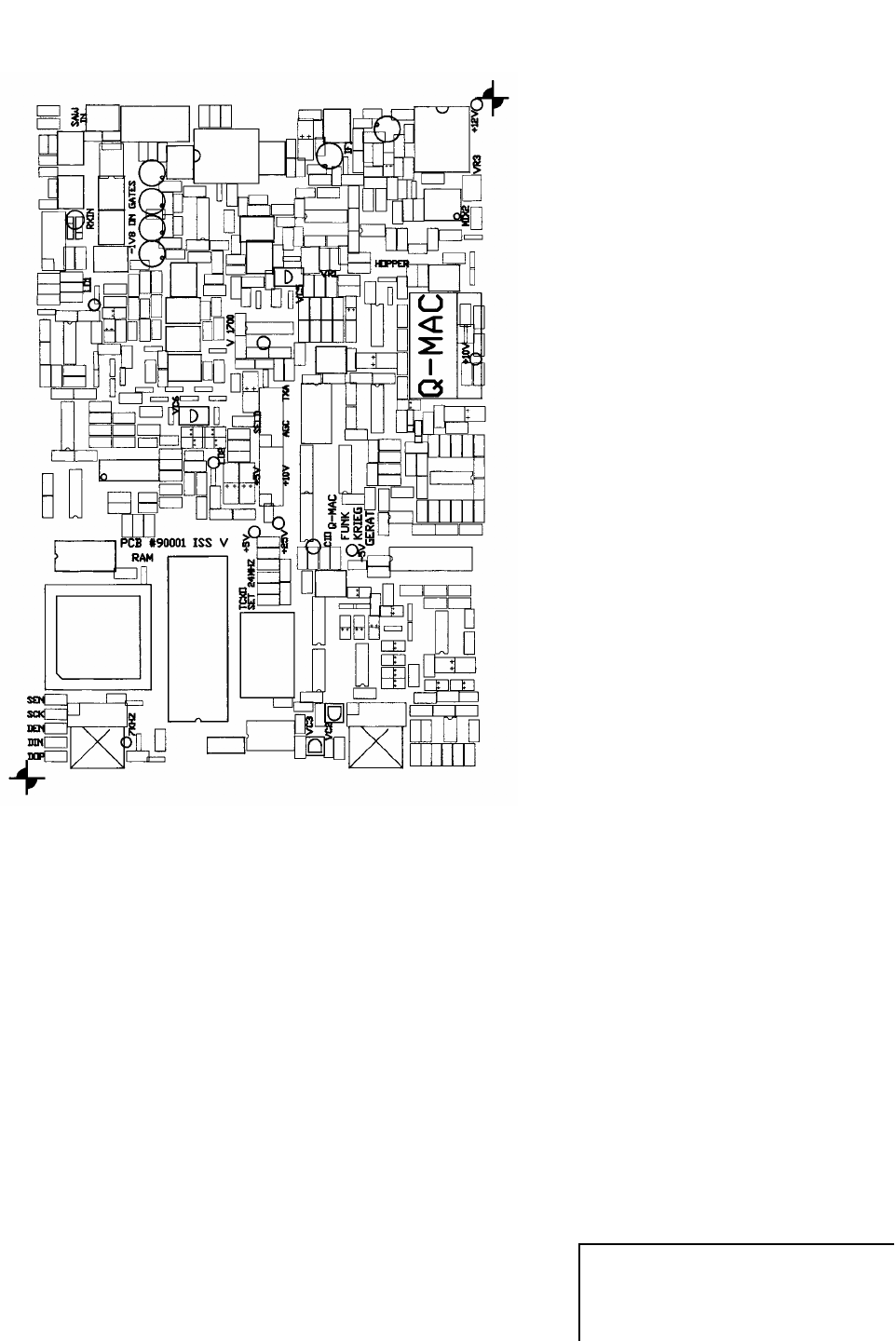
7.2 RXMP PCB
Refer to the schematic diagram (HF-90 I.F. STRIP , MICRO SECTION & SYNTH. 90003) in Section
17 of this manual. Applies to RXMP boards of issue U and beyond.
The RXMP PCB is the heart of the radio and condenses a high degree of functionality into a
small board area.
The two main functional blocks on this board are the microprocessor and the receiver. Large
sections of the receiver are re-used on transmit to generate the drive for the PASW PCB. This
minimises unnecessary replication of circuitry. The RXMP PCB measures 100mm x 147mm
and contains 30 integrated circuits.
Microprocessor architecture
A minimal number of components are used as a result of the following:
" Delegation of functionality to software, wherever possible.
" Extensive re-use of ports.
" Utilisation of a simple serial interface.
" Use of a microprocessor with embedded code and separate data memory.
The microprocessor core consists of the microprocessor (U1), the non-volatile data memory
(U2), and the low address latch (U3). D24 gates the battery backed RAM enabling it during
RAM reads and writes.
DTMF detector
The DTMF chip (U9) flags data valid on pin 14 when keys on the DTMF microphone are
pushed. The microprocessor activates the DTMFE line when it is ready to read the DTMF
code. The DTMF chip is memory mapped at address #8000H and diode D1 disables the
battery backed RAM when a DTMF read occurs.
A full table of microprocessor port allocations is shown in Table 1 (Section 8 of this manual).
Serial links
There are two separate serial data paths which share a common data and clock signal (TOC
and SCK) but have different enable lines (SYN and DIS).
One of these serial links has been described in Section 7.1 (Front panel PCB), however it
services other registers besides the display. It loops back onto the RXMP PCB and controls
the miscellaneous register and volume control. It then loops through the PASW PCB where
it controls the PA low pass filter selection and power selection. Finally, it loops back to the
microprocessor where it can be sampled to check the link.
The second serial data signal is the synthesizer loader. This is fed to U16 setting the
frequency of LO1 and LO2.
The display enable and clock are also used to increment the signal strength meter ramp
counter, which is active on every display write.
A hardware and software summary of these two serial links is contained in Diagram 1 and
Table 2, respectively (Section 8 of this manual).
- 17 -
Interrupts
The microprocessor runs three interrupts:-
1. The incremental shaft encoder interrupt on INT1 (volume set).
2. An internal software interrupt on Timer 0, TICKINT which wakes up the
microprocessor from an idle state every 2ms (or 666µs in hop mode). This is the
‘heartbeat’ of the radio and it ticks at all times except during computer
communication.
3. An internal software interrupt on Timer 1, TIMER1INT which provides timing for all
tones generated by the radio on receive and transmit.
The RS232 serial I/O programming link is not run as an interrupt driven service. It is
operated as a scheduled polled service.
Although PTT input to the microprocessor is fed into pin INT0, the interrupt on this pin is
disabled and instead the pin is polled. It is also a PTT output.
Shaft encoder
Quadrature drives to the shaft encoder from QUAD1 and QUAD2 allow the detection of
turning direction and velocity, by line INT1. The change in volume is output via the serial
link to the shift register (U11) setting the gain DAC (U13).
Clarifier
The clarifier on receive is implemented entirely in software adjusting the synthesizer in 25Hz
increments over ±250Hz.
Receiver and synthesizers
The receiver architecture comprises a double conversion superheterodyne with intermediate
frequencies of 83.16MHz and 455kHz. Two high-side local oscillators (LO1 and LO2) mix
down to 83.16MHz and 455kHz respectively.
The local oscillators are controlled by a dual frequency synthesizer which allow coverage of
2 - 30MHz in 100Hz steps.
Mixing scheme
Diagram 2 (Section 8 of this manual) shows the HF-90 superheterodyne mixing scheme.
Synthesizer Part 1
Synthesizer Part 1 controls LO1. The synthesizer chip (U16) utilises an internal dual
modulus prescaler to obtain a high operating frequency (85 - 113MHz), along with a high
phase comparison frequency (47 - 202kHz). The synthesizer is designed for low phase noise
and the loop filter (R25, C96, C99) is optimized for low phase comparison sideband level.
The high comparison rate gives the synthesizer a very rapid lock time of 3ms. The non-
linear amplifier (Q10, Q14, Q15, Q16, Q22) linearises the overall system gain to maintain
consistent noise performance across the VCO span.
- 18 -
LO1
LO1 is a high level (+13dBm) low phase noise VCO providing the injection source for Mixer
1. It employs push-pull JFETS (Q6, Q7) and an amplitude stabilisation circuit (D7, D8, Y1,
Y2, Y7, Y8). Fast inverters (U29 E and F) provide hard switching and load isolation.
Synthesizer Part 2
Synthesizer Part 2 (U16) employs a single chip synthesizer to stabilize the injection
frequency of LO2. It has an on-board prescaler and requires only the external loop filter
(C85, C77, R83, R4, C46). The frequency of LO2 is controlled in 200 100Hz steps over a
20kHz span.
LO2
LO2 employs a Vackar circuit with a very narrow span. It provides a +7dBm injection level
for Mixer 2 using a single JFET (Q8). A fast inverter (U30C) and a 3dB pad provide hard
switching and load isolation. Capacitor C212 is a 33p N470 type, to achieve temperature
compensation from -30ºC to +60ºC.
Front end
A 5-element elliptic low pass filter band limits the receiver input signal and suppresses
leakage from LO1 on transmit and receive.
A high-level GaAs FET mixer (Q1, Q2, Q3, Q4) provides a low loss, high 3IP performance
to obtain excellent sensitivity and dynamic range. This mixer incorporates proprietary
architecture. Being essentially a passive element, the mixer is reciprocal and operates in the
reverse direction in transmit mode. Diodes D14 and D27 provide front end protection.
First IF
The first IF chain comprises F1, Q5 & U21, with associated components. The active
components are switched in direction between receive and transmit by a relay pair (RL1 &
RL2). This ensures optimum IMD performance on both receive and transmit.
Saw filter
Selectivity with a bandwidth of 30kHz is provided by the first IF filter (F1). Use of a SAW
device allows very smooth passband performance with deep transmission zeros on the image
frequency of the second IF. The tank circuits associated with L5 and L6 provide impedance
matching for the filter which has a Zo of 800Ω.
Active devices (Q5 and U21) provide the AGC controlled gain in the first IF. The Op-Amp
(U20) stabilises the bias current in the GaAs FET. The GaAs FET is characterised by
excellent linearity and ultra low noise.
Mixer 2
The second mixer uses a diode ring module (M1) to mix to 455 kHz. Because it is passive, it
functions as a reciprocal device, operating in the reverse direction on transmit.
- 19 -
Filter 2
The ultimate selectivity of 2.4kHz @ 3dB points is provided by ceramic filter (F2). This
device has a Zo of 2kΩ. Matching on transmit and receive is performed by 5mm transformer
(T8).
Tx/Rx switch
Bilateral switch (U22) routes the signal through the final IF processor chip (U23) on receive
and direct from the double balanced mixer on transmit. It also handles the transmit and
receive audio paths ensuring correct audio switching to/from the double balanced mixer
(U24).
455 kHz IF processor
The IF processor chip (U23) provides up to 100dB gain at 455kHz and provides 100dB of
AGC range. U19C and Q11 along with C131, C22 and C174, implement hang AGC
appropriate to SSB signals. Two different decay times, fast and slow, are available by
switching MOS FET Q25.
Double balanced mixer
The double balanced mixer (U24) provides greater than 50dB of carrier suppression on
transmit and highly linear demodulation on receive. As previously described, bilateral switch
(U22) performs the signal routing to enable this to happen.
Carrier insertion oscillator
To generate and receive a single sideband signal a carrier insertion oscillator is required. On
USB this operates at 453.6kHz and on LSB the frequency is 456.4kHz. It is derived from
oscillator (U6), which has selectable crystals (X3 & X4). The oscillator operates on
7257.6kHz or 7302.4kHz for USB and LSB respectively. The CIO frequency emerges from
output Q4 of counter U7, after division by 16. Counter U7 also provides a 7kHz clock to run
the charge pump, 25volt & -5volt supplies and the display multiplex clock.
Gain distribution
Diagram 3 (Section 8 of this manual) shows the HF-90 system gain distribution.
Receive audio chain
The recovered audio of pin 6 of the double balanced modulator (U24) is routed through a
switch (U22) to the gain stage (U25B). This provides 30dB gain, taking AGC level signals
up to 2volt p-p.
The audio path feeds through the volume control DAC onward to the output amplifier (U28).
The DIL audio amplifier yields 2watt, or more if the radio is operating from higher than
12volt.
The amplifier (U27:B) provides a limiting signal to the Selcall decoder (U18).

- 20 -
Selcall decoder
The Selcall decoder uses an on-frequency PLL with a VCO centre frequency of 1700 Hz. An
XOR phase comparator (PCI) is used for noise rejection. The recovered data signal appears
on the loop filter (R32, R128, C127, C129). It is then fed to a data slicer which has an
adaptive reference level (pin 6 U19:A). This ensures that off-frequency signals will be
satisfactorily recovered since the reference is the mean signal deviation. The data is sent on
its way to the microprocessor as SELD.
The switching transistor (Q12) disables the Selcall output (SELD) when SELE is taken high
by output PL3/Pin 7 on the PASW PCB. This allows the computer the use of the FROMC
line during programming.
Microphone amplifier
The microphone amplifier (U25:A) provides a differential balanced input allowing common
mode rejection. Inputs from TR and BR allow tone modulation for the emergency alarm,
being added at the virtual earth. Input from the microphone is via a 600Ω transformer (T7)
which provides isolation. The microphone amplifier has a feed to DTMF chip U9.
Automatic audio level control
The ALC chip (U26) works on transmit to maintain a near constant output level of 2volt p-p
when the audio output is beyond a certain threshold set by R73. In this way the best radiated
signal to noise ratio is maintained. The transmit audio signal (TXA) is routed through U22 to
pin 4 of the double balanced mixed (U24). A diode clipper (D18,C173) prevents any
transient overshoot.
Receiver voltage supplies
The main +5volt supply is switch mode derived on the PASW PCB. The main +10volt
supply is from a linear regulator on the PASW PCB.
Low current supplies at +25volt and -5volt are derived from a charge pump circuit
(comprising U8, D2, D6, D16, D17 and D19). The charge pump is clocked at 7kHz by the
CIO counter (U7).
Low battery detector
The comparator (U4B and A) detects when the 10volt regulator loses regulation and pulls the
LOBAT line low, signaling low battery level. At present this signal is not used by the radio.
Signal strength meter
The signal strength meter comprises counter U14, DAC U15 and comparator U4:C. The
counter is clocked and enabled by the display serial line. During display write the counter is
clocked and when the DAC ramp crosses the AGC level comparator U4:C, output feeding
RCL is pulled low. In this way the microprocessor can measure signal level.
- 21 -
7.3 PASW PCB
Refer to the schematic diagram (HF-90 P.A. & POWER SUPPLY 90002) in Section 17 of this
manual.
This printed circuit board contains the power stages of the transmitter and all the radio power
supplies. It measures 100mm x 147mm and contains nine integrated circuits. Four MOS
FETS and two power transistors are mounted on the mechanically connected rear heatsink.
The HF-90 breaks new ground in obtaining excellent transmitter intermodulation distortion,
low broadband noise and PA economy, through the use of high voltage MOS FETs in the PA
and driver stages. The necessary supply rails are provided by low EMI switch mode power
supplies.
Power supplies
Tx supply switches
The darlington driver (U8) inverts the PTT / line to switch series pass transistor (Q11) which
keys up the +5 Tx supply.
+5volt supply
A simple switcher chip (U9) along with D10, L2 and C80, provide a high efficiency +5volt
output from a wide range of input voltages (10 - 28volt). Chokes (L1 and L3) with
associated decoupling capacitors minimise electromagnetic emission. The unit is enclosed
by a shield to further reduce interference.
+10volt supply
This relatively low current +10volt supply is obtained by sitting a 5volt regulator (U10) on
the +5volt rail. The regulator is a low dropout type requiring only 0.2volt of headroom.
+15volt supply
This supply should be more correctly designated the +11.4volt limiter since its function is to
maintain an output voltage in the range 10 - 11.4volt, irrespective of input voltage.
The series pass transistor (Q13) is hard on until U3:A detects that its output has risen to
+11.4volt. Thereafter it is held in regulation. It is keyed on only in transmit by using the
+5volt supply as a reference. Its function is to limit supply voltage to U4 and MOSFET
drivers (Q1 & Q2).
+50volt Tx supply
The +50volt Tx supply is a classic boost convertor utilising energy storage choke (L5),
switches (Q5 and Q6), and a rectifier (D5). The switch mode controller chip (U4) monitors
the output voltage via voltage divider (R7 & R8) comparing it against a 5volt reference to
obtain an error duty cycle on the gates of Q5 and Q6. The chokes (L4 & L6) with their
associated decoupling capacitors yield a low EMI design. Some supply droop will occur on
speech peaks.
Tx amplifier (pre-driver)
The current mode Op-Amps (U1 & U11) each provide +16dB of gain with low output
impedance, wide bandwidth and excellent linearity. They drive the driver MOS FET gates
through a balanced transformer (T4). the MOS FET (Q9) in the feedback circuit of U11
controls the stage gain. This permits ALC of the PASW unit.

- 22 -
Bias circuit
Bias for both the driver and PA MOS FETs is derived from a source which is effectively an
amplified thermal junction pedestal (Q8 and Q12). VR1 is the driver bias pot and VR2 is the
PA bias pot. These references are buffered by Op-Amps (U2:A and U3:B) which have gains
of three and five respectively. Device Q12 is in direct thermal contact with PA MOS FET
Q3, and device Q8 is in direct thermal contact with Q4 in order to obtain a thermal
coefficient of bias which is slightly negative, thus ensuring thermal stability.
PA drivers
The PA driver circuit uses MOS FETs (Q1 and Q2) running from the +15volt limited supply
(+11.4volt). Negative feedback networks (C57, R43, R90, C56, R88 & R44) fix the gain of
the stage at 20dB. The 10R input resistors (R37 & R55) suppress parasitics. The bifilar feed
transformer (T1) provides a DC cancelled supply isolation.
The transmission line transformer (T5) yields a 4:1 impedance step-down to provide final
output MOS FETs (Q3 & Q4) with a high current source for gate drive.
PA final output
The final output architecture is similar to that of the drivers, with negative feedback and
parasitic stoppers. The difference lies in the supply voltage and output matching. The PA
transistors operate from a +50volt rail, achieving isolation from supply by a DC cancelled
bifilar choke (T2). An output transmission line transformer (T3) combines the output signals
and provides balance-to-unbalance conversion. Impedance conversion is unnecessary since
the PA matches directly to 50Ω. Polyswitches (Negative TC Thermistors) in series with the
source leads of the output MOS FETs Q3 and Q4, wind back the output power when the
temperature on the heatsink exceeds 80°C.
PA low pass filters
Harmonic attenuation of the transmitter output signal is implemented through the six 5-
element elliptic low pass filters. Latching relays (RL3 - RL8) select the sub-octave filters
according to Table 3 (Section 7 of this manual).
Relay drive circuit
Selection of the set or reset coil for activation is implemented via seven darlington drivers
(U6). The address information is loaded down the DIS serial data line into a shift register
(U5) and this drives the darlington driver (U6). When a frequency change occurs the
common reset line is pulsed, then the specific set line is pulsed. In the static condition no
current is consumed by the relays. Latching takes place through application of a 5ms pulse.
Tx RF ALC
The forward and reverse current are sampled by a 16:1 current transformer (L19) and
detector diodes (D1 and D2). These provide references for the ALC circuit. Potentiometer
VR3 sets the power level by manipulating the fraction of signal fed to U3:B.
Low power select deactivates the +50V supply by grounding pin 2 on U4.
ALC time constants are determined by C34, R95 and R96. A diode (D3) combines the

- 23 -
forward and reverse signals and the Op-Amp (U2:B) provides system gain in the ALC
feedback loop. The gain controlled RF amplifier (U11) in the first stage of the PASW PCB
is fed with the ALC output signal via Q7.
ATU PSU switch
A software keyed +12 - 28volt supply is provided on the rear 4-pin connector to allow the
interfacing of a TA-90 automatic antenna tuner, a horn alarm or flashing beacon.
Reverse / over-voltage / under-voltage protection
A tranzorb diode (D7) provides reverse and 33volt clamp protection. An external fuse must
be fitted. Diodes D4 and D6, in series with the power on relay activation coil, ensure that the
radio will not power up if the supply is accidentally reverse polarised. The relay also
guarantees that the radio will switch off completely below 9.5volt, thus protecting the
connected battery against over discharge.
- 24 -
Table 1. HF-90 micro port allocations
Port Number Micro Pin Input Function Output Function
P0.0 43 D0 / DTMF Q0 A/D0
P0.1 42 D1 / DTMF Q1 A/D1
P0.2 41 D2 / DTMF Q2 A/D2
P0.3 40 D3 / DTMF Q3 A/D3
P0.4 39 D4 A/D4
P0.5 38 D5 A/D5
P0.6 37 D6 A/D6
P0.7 36 D7 A/D7
P1.0 2 TOP ROW TONE 1 OUTPUT
P1.1 3 SIG METER INPUT RIGHT COLUMN
P1.2 4 DTMF NOT VALID MIDDLE COLUMN
P1.3 5 LEFT COLUMN
P1.4 6 BOTTOM ROW TONE 2 OUTPUT
P1.5 7 SYNTH. CLOCK
P1.6 8 SYNTH. ENABLE
P1.7 9 DISPLAY ENABLE
P2.0 24 A8
P2.1 25 A9
P2.2 26 A10
P2.3 27 A11
P2.4 28 A12
P2.5 29 DTMF ENABLE
P2.6 30 (A14)
P2.7 31 (A15)
P3.0 11 RXD SERIAL DATA/
SELCALL IN
P3.1 13 TXD ALL SERIAL DATA
OUT
P3.2 14 INT0/PTT IN PTT OUT
P3.3 15 INT1/ENCODER
P3.4 16 T0 QUAD IN
P3.5 17 T1 QUAD IN
P3.6 18 WR EXT DATA
P3.7 19 RD EXT DATA
Note:- ALE latches Port 0 address
8. TABLES & DIAGRAMS
- 25 -
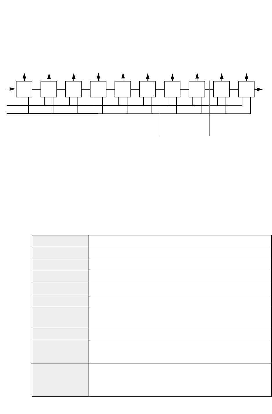
Diagram 1./Table 2. Serial link chain
Diagram 1. Physical hardware
The serial link chain comprises 10, 8-bit serial shift registers with common serial clock
(SCK), select display (DIS) lines and cascade data (TOC).
Serial data is clocked through the shift registers by SCK and when 80 bits of data have gone
through, the enable DIS is pulsed high and the data is parallel loaded to internal latches.
Table 2. Software byte allocation
Byte 0
100 Hz display
(last byte)
Byte 1
1 kHz display
Byte 2
10 kHz display
Byte 3
100 kHz display
Byte 4
1 MHz display
Byte 5
10 MHz display
Byte 6
Byte 7
Bits 0 to 7 volume in range 00H - FFH (LOW = LOW VOL)
Byte 8
Byte 9
BIT7
NIL BIT6
BAND1
BIT5
BAND6 BIT4
BAND2 BIT3
BAND5 BIT2
BAND3 BIT1
BAND4 BIT0
RESET PA Filter
Band
Select
Disable
loop-
back
Disable
Selcall NIL NIL +50V
OFF Low
power ATU
ON NIL
(1st byte)
Loop
Back
SCK
DIS
Front Panel PCB RXMP PASW
PASRO
(TOC)
SDIN
LED
100Hz LED
1kHz LED
10kHz LED
100kHz LED
1MHz LED
10MHz Miscellaneous
DAC Volume
DAC PA Filter
Switch Power
Setting etc.
BIT 0
1 = USB, 0 = LSB
BIT 6 BIT 1
1 = MIC INHIBIT 1 = AGC SLOW
- 26 -
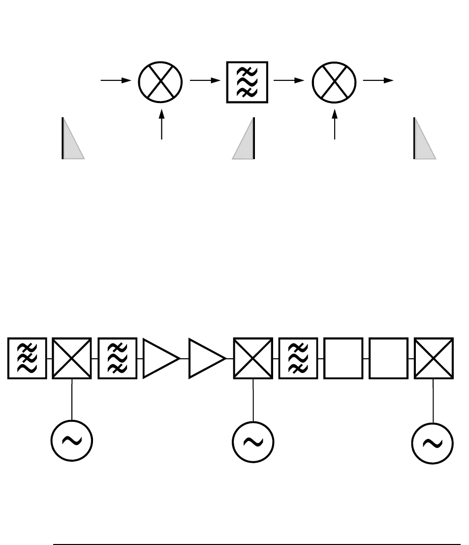
Sensitivity = 0.25uV @ 10dB S+N/N
3I/P = +20dBm
3dB AGC knee = 1uV
Diagram 2. Superhet. mixing scheme
3740 USB 453.6 CIO
86900 kHz
LO1 83613.6
LO2
Diagram 3. HF-90 Rx gain distribution
LO1
85.113 MHz
LO2
83.615 MHz
+/-10 kHz
CIO
USB 453.6 kHz
LSB 456.4 kHz
-0.5dB -5dB -4dB +20dB +20dB -8dB -6dB +16dB +80dB
LPF 4 x GaAS SAW
83.160 MHz
ATF
13736 ERA3
CERAMIC
455 kHz
TDA
1572
STAGE 1
TDA
1572
STAGE 2
- 27 -
Table 3. HF-90 Tx low pass filters
Truth table
Band HEX Code Causes 1 Causes 0
U5 Pin U6 Pin
RESET 01H 15 10
NULL 00H -
1 40H 6 16
2 10H 4 14
3 04H 2 12
4 02H 1 11
5 08H 3 13
6 20H 5 15
When the PA filter is selected, the high level (+5V) on U5 pin persists for only
three seconds. After this time the voltage on all U5 output pins reverts to zero.
The latching relays preserve their current state.
Relays may be selected manually by first resetting (ie. shorting pin 10 of U6 to
ground momentarily) then shorting the relevant pin (11-16) on U6 momentarily
to ground, to select the desired filter.
Note:-

- 28 -
Table 4. HF-90 connector pinouts
Pin Code Function Used on
(source underlined)
1 QUAD 1 QUAD ENCODER IN 1 FP / RXMP / PASW
2 QUAD 2 QUAD ENCODER IN 2 FP / RXMP / PASW
3 DISRO DISPLAY SHIFT REG OUT FP / RXMP / PASW
4 FROMC SERIAL DATA IN
(FROM COMPUTER) FP / RXMP / PASW
5 SCK SERIAL CLOCK FP / RXMP / PASW
6 GND GROUND FP / RXMP / PASW
7 DIS DISPLAY ENABLE FP / RXMP / PASW
8 +5 +5 SUPPLY FP / RXMP / PASW
9 TOC GENERAL SERIAL DATA OUT
(TO COMPUTER) FP / RXMP / PASW
10 7 kHz DISPLAY MPX CLOCK FP / RXMP / PASW
1 MCL MIDDLE COLUMN FP / RXMP / PASW
2 LCL LEFT COLUMN FP / RXMP / PASW
3 RCL RIGHT COLUMN FP / RXMP / PASW
4 TR TOP ROW FP / RXMP / PASW
5 BR BOTTOM ROW FP / RXMP / PASW
6 MIC1 MICROPHONE 1 FP / RXMP / PASW
7 MIC2 MICROPHONE 2 FP / RXMP / PASW
8 ON/OFF ON/OFF FP / RXMP / PASW
9 PTTU PTT UNBUFFERED FP / RXMP / PASW
10 LS LOUD SPEAKER FP / RXMP / PASW
1 PASRI PA SHIFT REG IN RXMP / PASW
2 PASR0 PA SHIFT REG OUT (SELD) RXMP / PASW
3 SCK SERIAL CLOCK RXMP / PASW
4 DIS DISPLAY ENABLE RXMP / PASW
5 +5 +5 SUPPLY RXMP / PASW
6 +10 +10 SUPPLY RXMP / PASW
7 SELNE SELCALL DISABLE RXMP / PASW
8 GND GROUND FP / RXMP / PASW
9 GND GROUND FP / RXMP / PASW
10 GND GROUND FP / RXMP / PASW
Con: PL1
SERIAL
QUAD
Con: PL2
KEYS
MIC
LS
Con: PL3
POWER
SIGNALS
- 29 -
Pin Code Function Used on
(source underlined)
1 GND GROUND FP / RXMP / PASW
2 +24 +24 RELAY SWITCHED RXMP / PASW
3 GND GROUND FP / RXMP / PASW
4 +50 +50 TX SUPPLY RXMP / PASW
5 +15 +11.4 LIMITED TX SUPPLY RXMP / PASW
6 PA BIAS PA BIAS (3.9V) RXMP / PASW
7 RFI0 RF INPUT/OUTPUT RXMP / PASW
8 DR BIAS DR BIAS (2.2V) RXMP / PASW
9 GND GROUND FP / RXMP / PASW
10 ALC ALC MONITOR RXMP / PASW
1 NOT USED
2 GND GROUND FP / RXMP / PASW
3 NOT USED
4 AGC RX AGC OUT RXMP
5 SELD (PASRO) SELCALL DATA RXMP
6 GND GROUND FP / RXMP / PASW
7 GND GROUND FP / RXMP / PASW
8 RXA RX AUDIO RXMP
9 SELA SELCALL AUDIO RXMP
10 TXA TX AUDIO RXMP
1 ROMOE ROM OUTPUT ENABLE RXMP
2 WR ROM WRITE RXMP
3 ROMCE ROM CHIP ENABLE RXMP
4 12 MHz 12 MHz CLOCK RXMP
5 ALE ADDRESS LATCH RXMP
6 DTMFE DTMF ENABLE RXMP
7 A0 ADDRESS 0 RXMP
8 A3 ADDRESS 3 RXMP
9 A1 ADDRESS 1 RXMP
10 A2 ADDRESS 2 RXMP
Con: PL4
PA
MONITOR
Con: PL5
RXMP
SIGNAL
TEST
SOCKET
Con: PL6
RXMP
MICRO
TEST
SOCKET
See below
*
* PL6 not present on RXMP issue M and beyond (S/No 1400→
→→
→).
- 30 -
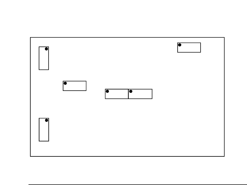
Diagram 4. Connector positions
COMPONENT SIDE OF RXMP PCB
PL2
PL6 *
PL3 PL5
PL4
PL1
* PL6 not present on RXMP issue M and beyond (S/No 1400→
→→
→).

- 31 -
9. MAINTENANCE
9.1 Disassembly and assembly
A. Removal of PCBs
First undo the four M3 screws on the rear heatsink. Take care not to lose the insulating
bushes. Slide the heatsink assembly complete with PASW and RXMP boards out of the
extruded sleeve.
B. Separation of PCBs
The PASW and RXMP PCBs mate via four 10-way connectors. These hold the boards
firmly together. It is best to separate the boards by taking one board in the left hand and the
other board in the right and using the fingers as levers to gently prize the boards apart in a
controlled manner.
C. Removal of the front panel
Undo the four M3 screws on the front panel. Take care not to lose the three plastic bushes.
The display PCB is held on to the front panel by the nuts of the on/off switch, microphone
socket and volume encoder.
D. Reassembly of radio
It is advisable to commence reassembly with the RXMP and PASW boards first. Make sure
that the boards are firmly together and that the rear rubber gasket is in place. Slide the 2-
board ‘sandwich’ into the sleeve making sure that the correct orientation has been selected.
The small aluminium heatsink on the PASW board has a keyway which engages in the
extruded sleeve. Tighten the screws on the rear heatsink evenly, making sure that the gasket
is correctly placed. Finally, replace the front panel making sure that the two 10-way
connectors engage properly on the RXMP board. Tighten the four M3 screws taking care to
position the gasket correctly.

- 32 -
9.2 Replacement of Microprocessor
In the event of firmware upgrade or in the extremely unlikely event of corruption (leading
character of software version display is “E”), the microprocessor chip U1 will require
replacement.
A number of precautions should be observed during this procedure.
" The correct PLCC 44 “scissor squeeze” type of extraction tool MUST be used.
" Removal and insertion must take place at an antistatic workstation.
" Orientation of U1 is critical with PIN 1 dot nearest to edge of RXMP board.
" This chip determines whether or not radio has a hopping option fitted.
- 33 -
9.3 Radio alignment
RXMP board
Refer to the test point overlay (HF-90 RECEIVER BOARD ALIGNMENT - POSITION REFERENCE)
in Section 12 of this manual, as well as the schematic diagram (HF-90 I.F. STRIP , MICRO
SECTION & SYNTH. 90003) in Section 17 of this manual.
1. Set the radio to any channel where its frequency is exactly divisible by 20kHz, ie
frequency ending in 00, 20, 40, 60, 80.
2. Using a digital multimeter measure the voltage at TPLO2. Adjust VC5 until this
voltage is 2.3volt +/-0.1
3. Set the radio to 30,000kHz
4. Using a digital multimeter measure the voltage at TPLO1. Adjust VC6 until this
voltage is 20volt +/-0.5
5. Using a frequency counter with high impedance probe measure the frequency at
TP24MHz. Check that the radio has been running for two minutes. Set the frequency
to 24MHz +/-7Hz by adjusting the TCXO.
6. Check that a USB channel has been selected. (no indicator point lit next to highest
digit).
7. Using a frequency counter with high impedance probe measure the frequency at USB/
LSB TP. Adjust VC3 to obtain 453.6kHz +/-3Hz.
8. If the radio has software for the export market ie HF-90E then select an LSB channel.
9. At the same USB/LSB test point measure the frequency and adjust VC2.
" On radios with Serial Number below 1200 measure 456.6kHz.
" On radios with Serial Number of 1200 and above measure 456.4kHz.
10. On PL5 fit a 10-way receptacle which has pin 7 connected to pin 9 via a 100nF
capacitor. Using a frequency counter with high impedance probe, measure the
frequency at TP1700Hz (U18 pin 3 & 4). Adjust VR1 until the frequency is 1700Hz
+/-8Hz.
11. Using an oscilloscope with 10:1 probe, measure the voltage on USB/LSB TP. Adjust
core T10 for maximum. This corresponds to approximately 1.7volt p-p.
12. Select a channel somewhere in the 5 - 8MHz region. Turn up the volume and with no
antenna or signal generator connected, adjust the AGC threshold control (VR2)
clockwise just beyond the point where there is no increase in noise. RXMP boards
beyond issue S do not require this adjustment.
13. Inductors L1 and L2 should be left at the factory setting. The core position will be
approximately 2mm below the coil top.
14. Apply a signal at 1kHz above the channel frequency to obtain a 1kHz tone. Set the
level to 0.25µv and monitor the loudspeaker recovered audio on an oscilloscope.
15. Adjust L5 and L6 to obtain a peak in the tone. L6 will probably be screwed further in
than L5. Neither adjustment is very critical.
- 34 -
16. Adjust L11 to obtain a peak in the tone. This will probably be quite sharp.
17. Adjust L7 to peak the recovered tone. The core may be screwed up until it is starting
to emerge from the coil. Do not allow it to protrude more than 1mm above the coil.
18. Adjust T9 to obtain a peak in the tone. The signal to noise may be slightly improved
by turning the core slightly clockwise beyond the peak.
It should now be possible to measure 10dB S+N/N on the 0.25µv signal.
The receiver alignment is now concluded.
PASW board
Refer to the test point overlay (HF-90 P.A. BOARD ALIGNMENT - POSITION REFERENCE) in
Section 12 of this manual, as well as the schematic diagram (HF-90 P.A. & POWER SUPPLY
90002) in Section 17 of this manual.
1. There are only three adjustable potentiometers on the PASW board and with two of
them (VR1 and VR2) the bias settings SHOULD NOT BE TOUCHED unless a driver
or final amplifier transistor has been changed.
2. Connect the HF-90 to a power meter and dummy load. The wave form can be
monitored by ‘eavesdropping’ on the coaxial line using an asymmetric Tee pad. This
consists of a 1K 1watt resistor connected to the 50Ω line. The other end of the resistor
is connected to the oscilloscope input and a 47Ω resistor must be connected across the
oscilloscope input. The above network yields approximately 30dB attenuation.
3. Inductor L20 should not be adjusted. It should remain as factory set with core 1mm
below the coil top.
4. Potentiometer VR3 is the ALC power level setting pot. It should be set on a channel
in the 4 to 6MHz range to give a clean 2-tone signal of the required power level (50-
60watt). On Australian models (HF-90A) a 2-tone signal can be obtained by holding
down the ALARM key for two seconds. The control VR3 is typically adjusted near to
the anti-clockwise end-point. Note that if the power level is backed off, a ‘bubbling’
effect can occur. This can be alleviated by screwing in core L7 slightly or adjusting
VR3 on the RXMP board. It may also be necessary to do this when swapping PCBs.
5. In the event of either driver or final amplifier MOS FETs having been changed, the
bias can be set up as follows:
" First remove the two jumper links on the back of the PASW board.
" Using a multimeter on the 10volt range, measure the voltage on the positive end
of C49 (10µF tant).
" Push the PTT switch and adjust VR1 to obtain 2.6volt.
" Measure the voltage on the positive end of C63 (10µF tant).
" Push the PTT switch and adjust VR2 to obtain 3.7volt.
" Now replace the jumpers under the PASW board.
Changing a final amplifier transistor
Should either of the final amplifier MOS FETs Q3 or Q4 require changing, the following
procedure should be followed:
1. First check the manufacturer of the replacement. IRF830 devices from Motorola (M),
Harris (H), International Rectifier (IR) and SGS-Thomson (S or ST) have been used.
If the replacement is not the same manufacturer as the original parts, then both devices
MUST be replaced.

- 35 -
2. Loosen off the M3 screw securing the power device. Carefully remove the screw and
swing away the thermal protection transistor Q8 or Q12 on its flying lead. The
SILPAD between the thermal sensor and the output device must be kept. Next
desolder all three legs of the defective device. Remove the device taking care to
preserve both the SILPAD under the device flange AND THE TINY PLASTIC
SLEEVE WHICH SPACES THE FLANGE FROM THE SCREW. Note that a
polyswitch disc thermistor may be fitted in series with the source lead of each output
transistor Q3 and Q4. These should not be removed. If they are not fitted (two yellow
discs) contact Q-MAC Electronics for advice on fitting as per ECN 79 and 80.
3. Having removed the device, simply reverse the process with the new device taking
care to fit all the parts correctly (two SILPADs plus plastic sleeve). The M3 screw
should be firmly tightened.
IMPORTANT NOTE:
THIS PROCEDURE SHOULD ONLY BE ATTEMPTED BY QUALIFIED SERVICE
PERSONNEL. Q-MAC ELECTRONICS WILL CHARGE FOR ANY DAMAGE CAUSED BY
INCORRECTLY IMPLEMENTING THIS PROCEDURE.

- 36 -
10.1 No tools fault finding
Fault diagnosis
1. Check that the 4-pole power connector on the rear of the radio is correctly connected
to a 12 - 24volt power source (battery or power supply) capable of providing 10ampere
peak current. Screw up the locking ring. Ensure correct polarity. Refer to the table
below if in doubt.
2. Check that an approved antenna or 50Ω dummy load is connected to the rear BNC
coaxial socket.
3. Connect the microphone to the front 8-pole receptacle. Screw up the locking ring.
4. Connect the loudspeaker to the 4-pole spur connector on the rear cable if required.
ENSURE THAT THE CORRECT POLARITY IS OBSERVED
5. Switch ON/OFF switch to the ON position and check that the following power on
sequence occurs.
Power-on Sequence
Elapsed Time Display Contents Loud Speaker Internal Sounds
Start Blank Click Relay Click
1 second HF-90A or HF-90E
or HF-90H 1kHz Tone Relay Click
2 seconds Software Revision
eg. 2-407
or if error E2-407
Silence or if error
900Hz Tone Relay Click
3 seconds Selcall Number if
Advanced Model eg.
1234
Radio Noise Relay Click
4 seconds Channel Number eg.
CH 2 Radio Noise Relay Click
5 seconds onward Frequency display
if HF-90E or HF-90H Radio Noise Silence
6. If the radio is completely dead, ie. no tones, clicks, loudspeaker noise or display, then
suspect that no power is getting through to the rear connector. If this is not the case
then possibly the wiring at the rear of the front panel ON/OFF switch is faulty, or the
two front panel 10-way connectors may have been mis-engaged during the last re-
assembly.
10. FAULT FINDING

- 37 -
7. If a display is present on turn-on, but the software revision comes up with a program
memory checksum error (eg. E2-407), accompanied by a 900Hz tone from the
loudspeaker, then some degree of memory corruption has occurred. The radio should
be fitted with a new microprocessor available from an authorised dealer or Q-MAC
Electronics Pty Ltd. The microprocessor is the only pluggable component on the
RXMP PCB. Some radio functionality may be unaffected by the corruption.
Corruption is highly unlikely to occur.
8. If the display is normal on turn-on and the sequence of five relay clicks can be heard
from inside the radio, but no loudspeaker tones or noise of any sort is heard, then
suspect a problem with the external loudspeaker connection. If the loudspeaker and
wiring are in good condition then the internal loudspeaker feed wire or tracks on the
RXMP or PASW PCBs may be broken or short-circuited. If a speaker microphone
produces audio but a loudspeaker does not, then the loudspeaker track on the PASW
PCB has been broken. Check that the loud speaker plug has been correctly inserted.
9. If the display is blank or has unintelligible characters, but the turn-on sequence of
tones and relay clicks is correct, then the microprocessor is probably operating
correctly but the display multiplexor clock (7kHz) is absent. This signal is generated
on the RXMP PCB.
10. If no clicks other than the first power relay click are heard, and no tones are audible
and either no display or incorrect characters are shown, then the microprocessor is
probably not running correctly. Some faint noise from the loudspeaker may be audible
in this condition. Replacing the RXMP PCB should fix the problem.
11. If the display comes up normally and tones are heard, but the sequence of relay clicks
is absent, then the serial data chain is broken somewhere. Turn the volume control up
and down and if this works then the break is between the RXMP and PASW PCBs. If
the volume is not working then the break is between the DISPLAY and RXMP boards.
Board substitution will confirm this.
12. If switch-on tones and clicks are normal but no radio noise is audible then there may
be a receiver fault. With the volume control at maximum a reasonable amount of noise
should be heard. The volume control gives clicks when it is being turned up or down.
At maximum or minimum, no more clicks will be heard. A high pitched whine may
indicate a fault in the -5v supply. If the problem has not been located substitute the
RXMP PCB.
13. Pressing the CHAN∧ or CHAN∨ keys should produce an internal click and the display
should show the next channel number. Some change in the character of the noise from
the loudspeaker may occur. If only UP or DOWN works then suspect a key or matrix
fault on the DISPLAY board. If it is a matrix fault then it will affect a whole row or
column of keys.
14. Press the PTT switch on the microphone. Listen for an internal relay click. Check that
the display changes to exhibit the frequency in kHz with decimal point illuminated. If
neither occurs then a fault in the microphone PTT switch should be suspected. If this
is not the case then the internal PTT circuit is faulty. If the frequency display is not
accompanied by a click, then the microprocessor is responding correctly but the PTT
feed to the changeover relays is faulty. If there is no display change but a relay click is
audible then the PTT input of the microprocessor has been damaged and a new micro
will be required. Replace the RXMP board.

- 38 -
15. Press the TUNE key briefly. The PTT relay clicks should again be heard. This time
the microprocessor is activating the PTT.
16. Program the radio with CH9999 (23999kHz USB). A strong 1kHz tone should be
audible on this channel. This is the 24MHz microprocessor clock. If it can be heard
then:
" The microprocessor clock is running.
" The receiver is functioning.
17. If the receiver is working but the transmitter is giving no power, then the internal HV
fuse on the rear surface of the PASW board may have ruptured. The fuse is
implemented as a meander track on the PCB. It should be replaced with 20mm of
0.16mm enameled copper wire.
18. Hold down the TUNE key for 20 seconds. The rear heatsink should start to get
significantly warm compared to the receive condition. If this is not the case then the
TX current is abnormally low. Again the HV fuse should be checked.

- 39 -
11. DIAGNOSTIC TEST SEQUENCE
11.1 Receiver test sequence
Refer to the test point overlay (HF-90 RECEIVER BOARD ALIGNMENT - POSITION REFERENCE)
in Section 12 of this manual, as well as the schematic diagram (HF-90 I.F. STRIP , MICRO
SECTION & SYNTH. 90003) in Section 17 of this manual.
The checks below should be made with the radio on receive with a USB channel in the range
3 - 6MHz selected.
1. Check the rails on RXMP
+5volt
" If dead, then check inverter on PASW.
" If high, then check for short between middle pin and output on U10 PASW.
+10volt
" If dead, then check that U10 PASW is properly connected.
+5volt output U31 RXMP
" If low, then open R80, R108 and R111 to see which is loading supply.
+5volt output U32 RXMP
" If low, then open R87 to see if it is loading supply.
+3v6 supply R133
" If high, then check for open circuit LED Y3, Y4.
-5volt supply
" If low, then check for loading by opening R150 RXMP. If this makes little difference,
then suspect charge pump or CIO.
+25volt supply
" If low, then check for loading by opening R137 RXMP. If this makes little difference,
then suspect charge pump or CIO.
2. Check clocks on RXMP
TP24MHz
" If clock is absent or low, then open R101 then R187 to check for loading.
" If the clock is absent after opening R101 and R187 then replace TCXO.
USB/LSBTP
" Using an oscilloscope check that the wave form at this point is approximately 1.7volt
p-p at 453.6kHz. It should be approximately sinusoidal.
" If no signal is present, check for a 7257,6kHz square wave at U6 pin8 (74HC00D). If
nothing is present then the CIO has stopped. If the wave form is there, then U7 (the
74HC4040) is at fault.
7kHz clock
" Using an oscilloscope, check the wave form at U7 pin14 (74HC4040). This should be
a 7kHz square wave and without it the display multiplexor and charge pumps will not
run.
- 40 -
U18 pins 3 and 4
" Using an oscilloscope check for the presence of a noisy square wave at an average
frequency of 1700Hz.
" In the absence of this, check the supply to the chip and the timing components C28,
R30, R127, VR1.
ALE on U4 pin 1
" This wave form is the ‘heart beat’ of the radio. If it consists of bursts of logic high
going pulses every 2ms during normal operation or every 666µs whilst hopping, then
the microprocessor is basically healthy. It is executing instructions correctly and
responding to the Timer 0 interrupt. It is also idling correctly. This wave form shows
how ‘busy’ the microprocessor is at any point in time.
" If the wave form is incorrect maybe an interrupt is stuck or the one of the buses has a
fault.
3. Check the synthesizer control voltages
LO2 TP
" Using a multimeter or oscilloscope, check that the voltage on this point is in the range
2 - 3volt. It should also be clean.
" If it is out of range then check that VC5 has not been damaged. Reset VC5 if
necessary as per Section 9.3 (Radio alignment).
LO1 TP
" This control voltage should start off low at 2MHz (2 - 3volt approx) and increase
towards 20volt at 13MHz. By 14MHz it should be back low again and increase back
up to 20volt at 30MHz.
" If there is noise or a sawtooth on the wave form inspect C96 and C99 for damage. Bad
connections to T12, T13 and T5 will also cause problems.
" Above 5MHz check that at least two of the four LO1 LEDs are lit. If not then LO1 is
dead or LO1 TP is at a very low value with the loop out of lock.
4. Check for correct DC voltages around the RXMP
GaAs FET gates Q1 and Q2, Q3 and Q4
" Check for approximately -1.8volt at both these points. This voltage is present only if
LO1 is running correctly (although not necessarily in lock) AND if all the GaAs FETs
are intact.
" If both points are slightly positive and all four LEDs in LO1 are extinguished, then
there is a problem with LO1 activity. Check T12, T13 and T5.
" If one point is normal and the other slightly positive, then it may be due to asymmetry
in LO1 or one or two defective GaAs FETs. Check also one end of R91 and R104 for
2.5volt bias and check U29 gate E and F levels (approximately 2volt average). U29
runs warm.
Q5 (ATF13736) gate
" This should measure -0.7volt approximately and the drain +2.8volt.
" If this is not so, then either the -5volt charge pump derived rail is not correct, or
feedback stabilising amplifier U20:B (LM358D) is faulty. U20 should have +2.8volt
on both pins 5 and 6.
Q21 (SST309) source
" This should measure +8.7volt approximately. If this is not the case then Op-Amp
U20:A is faulty.
- 41 -
Pin4 of F2 (the 455Khz filter at the end furthest from T8)
" This should have 2.5volt present. If not then R48 or R49 are faulty.
U23 pin 12 (TDA1572T)
" This should have 5.9volt with 0.5volt p-p of noisy 455kHz signal present.
" If not check for 2.2volt on pin 1 of U23 and 2.2volt on pins 3 and 4.
AGC monitoring point (on plus terminal of C22)
" This should be 2volt with no signal and rise to a maximum of 3.8volt with a huge
signal.
" If it is stuck high then check that AGC transistor Q11 is functioning.
Bias voltages on U24 (MC1496D)
" Pins 6 and 12, the outputs should be at 7volt.
" Pins 8 and 10, the CIO ports should be at 3.8volt.
" Pins 1 and 4, the signal input ports should be at 1.7volt.
" Significant discrepancies will likely be due to faulty resistors in the biasing chain.
" Injection at 453.6kHz should be visible at pin 8 of U24 (MC1496D) at a level of
approximately 0.3volt p-p.
RXA PL5 pin 8
" This should have a DC level of 3.6volt and a very low level recovered audio signal.
" If the DC level is incorrect then the bias pedestal set by R133, Y3 and Y4 is probably
faulty.
" If no audio is making it through the TX/RX switch ,U22 (4053D), then possibly it has
been damaged or the PTT level reaching pins 9,10 and 11 may be incorrect.
" Finally, damage to R178 or C200 may disable the switch path.
VOLI on pin 7 of U25 (LM358M)
" This should again be at a DC level of 3.6volt with a maximum recovered signal of
1.2volt p-p when a signal at full AGC level is applied.
U13 pin 8 (DAC0800M)
" This should have a DC level varying between 5volt at minimum volume and 3.3volt at
maximum.
" Failure of the DC level to correctly follow the encoder may be due to loss of the -5volt
bias on pin 7 or a failure of the serial data to correctly reach U11 (74HC595D).
U27
" This Selcall audio amplifier has a gain of 100 and should have clipped noise present on
pin 7 of U27 (LM358M).
U28 pin 14 (LM384N)
" This should have full supply voltage typically 14volt, otherwise resistor R172 has
failed.
U28 pin 8 (LM384N)
" This should have half supply voltage typically 7volt, with the full audio output present
under received signal conditions.
SELA pin 9 PL5
" This should exhibit almost rail to rail noise on an unoccupied channel. The average
voltage should be 2.5volt.

- 42 -
5. Serial digital wave forms can be checked
Channel change
" This should provoke activity on SYDA (DOP), SYCK (SCK) and SYEN (SEN) on
resistors R17, R13 and R12 respectively. Refer to schematic for wave forms.
Volume control change
" This should provoke activity on DIS (DEN) R14 and on SYCK (SCK) and SYEN
(SEN) as the serial data is sent down the chain to the volume control shift register U11
(74HC595D). However after the control reaches the ‘software endstop’ no further data
will be seen.
" Note that SYEN (SEN) pulses are very few and narrow.
" The volume encoder wave forms to the microprocessor can be checked on pins 1 and 2
of PL1. These are normally high but pulse low with shaft rotation.
SELD pin 5 PL5
" On a Selcall channel check for multiple data transitions on incoming noise.
" When receiving a Selcall the data on SELD should display a periodicity of 10ms.
Pin 13 of the micro U1 (89C738)
" All serial data from the microprocessor, for the synthesizer or the serial data chain or
for the computer during frequency programming emerges from pin 13 of the micro U1
(89C738).
U1 at pin 11
" All serial data to the micro from the Selcall decoder or from the computer during
frequency programming or from the serial chain loopback when enabled enters the
micro U1 at pin 11.
Keypad
" Keypad reading strobes emerge on pins 1, 2 and 3 of PL2 MCL, LCL and RCL.
These are short negative going pulses at 250Hz repetition rate.
" When keys are pressed in the matrix, either TR or BR pins 4 or 5 PL2 will be strobed
low.
" If all seems to be well yet keys are not being read check for shorts between the column
lines MCL, LCL and RCL.
DTMF keys
" Pressing keys on the DTMF microphone on an advanced model should produce a high
level on DV pin 14 of U9, (MC145436D).
" If this does not happen check that the DTMF tones at level 0.5volt p-p are reaching U9
pin 8.

- 43 -
11.2 Transmitter test sequence
Refer to the test point overlay (HF-90 P.A. BOARD ALIGNMENT - POSITION REFERENCE) in
Section 12 of this manual, as well as the schematic diagram (HF-90 P.A. & POWER SUPPLY
90002) in Section 17 of this manual.
For these tests the radio should be connected to a power meter and dummy load via a 30dB
asymmetric Tee off to an oscilloscope. A channel in the range 3 - 6MHz should be chosen
for measurements.
6. Transmitter Power Supplies
" Press PTT and check that +5voltTX is present on pin 5 of U3 (LM358M). If not check
Q11 and D10.
" Press PTT and check that +15voltTX is present in the range 10 - 11.4volt on collector
of Q13 (BD136 on heatsink). If not check Q13 and U3:A bias voltages.
" Press PTT and check that +50volt rail comes up to approximately +55volt. Some sag
of this rail is normal on speech peaks and Selcalls. If +50volt rail remains at 14volt on
transmit, check first that the channel program does not specify low power and then
check for 25kHz switching wave forms on R2 and R3.
" A 3-step wave form which varies with duty cycle should be visible on the anode of
diode D5 in the centre of large toroid L5.
7. Lowpass filter selection
" The low-going lowpass filter selection pulses to the latching relays are emitted on pins
10 to 16 of U6 (ULN2003L). On a channel change, the common RST line is pulsed
and then the band of choice is pulsed. As the driving device is open collector, the lines
may be manually pulled low to test for switching by momentarily shorting the relevant
pin to ground. Refer to Table 3 (Section 8 of this manual) which details the expected
state on pins of U6.
" For the filters to operate correctly the serial data chain must be intact all the way to U7
pin 9 (74HC595D), and serial data should be visible on this pin during a channel
change.
8. Bias check
" Check that the bias settings for driver and PA are approximately 2.6volt on C49
positive and 3.7volt on C63 positive with PTT active.
" Check that Op-Amp outputs U11 pin 6 and U1 pin 6 are approximately half rail (6volt)
with PTT active and no modulation.
9. Signal check
" Apply a fully modulating 2-tone by external means.
" The 2-tone envelope should reach 0.8volt p-p on U11 pin 6, 6volt p-p on U1 pin 6,
3volt p-p on the gates of Q1 and Q2 (VN88AFDs), 7volt p-p on the gates of Q3 and
Q4, 70volt p-p on the drains of Q3 and Q4 (IRF830s) and finally 140volt p-p at the
output of T3. Note that these values are approximate and are most accurate in the rage
3 - 6MHz.
" For the above levels, the rectified ALC wave form at U3 pin 7 should be
approximately 9volt peak. A similar voltage should be present on the gate of Q9
(BSD22).
" If signals are larger than above up to a stage and then very small thereafter, then the
first stage with the small signals is the one to suspect.
" Study the wave forms shown on the schematic carefully.

- 44 -
12. TEST POINT OVERLAYS
Please refer to the following pages for test point overlays .....
- 45 -
12.1 RXMP test point voltages
- 46 -
REFER LAYOUT DIAGRAM
“HF-90 P.A. BOARD ALIGNMENT POSITION REFERENCE”
IN FILE NAMED “PAHTPNOT.xxx”

- 47 -
13.1 Program description
Note:
For details concerning functionality, the HF-90 Operation & Installation Guide should be
consulted.
For details of the programming software, the HF-90 Programming Guide (Q-MAC Part No.
QM1001/2) should be consulted.
This section simply gives a broad view of how the radio software is structured.
START
INITIALISATION
MAIN LOOP
JUMP IF PTTON
CALL CHECK SELCALL
CALL CHECK KEYPRESS
CALL CHECK VOLUME
PTTON
CALL CHECK PA LOWPASS
CALL CHECK DISP TIMEOUT
CALL CHECK PTT
IDLE UNTIL INTERRUPT
JUMP MAIN LOOP
When the radio is not in computer control, the micro executes the above code every time it is
interrupted by one of the following:
1. Another Selcall one fifth bit period elapsing (every 2ms). -You can see this occurring
on ALE!
2. If tones are active on receive as a Selcall alert, in transmit as Selcall tone generation or
revertive tone generation. (approx every 300µs- depending on tone frequency)
3. If the volume control is being turned. (occasionally).
13. SOFTWARE OVERVIEW
- 48 -
13.2 Routine description
Volume
Checks if shaft encoder has moved and updates value to be sent to DAC if it has. (Note that
incoming Selcall has priority over this)
Keypress
Checks the 6 keys in the matrix:
" If CHAN∧ or CHAN∨, calls routine which updates synthesizer and display.
" If CLAR∧ or CLAR∨, calls routine which updates clarifier DAC and display.
" If TUNE, calls routine which pulls PTT low, updates synthesizer & display and
generates 1kHz tone.
" If ALARM/MODE, then USB/LSB bit toggled and synthesizer & display updated.
DTMF keys
The DTMF keys are checked and the values passed to the SELCALL command line
interpreter.
Selcall
If the radio is in receive and the channel is a Selcall channel then the Selcall decoder
algorithm is active.
This algorithm samples every fifth bit, filters the bit stream, looks for a dot pattern, then goes
on to detect sync and countdown, rephasing as necessary, detects the caller ID and attempts
to match the destination ID with its own. The following telephone digits are stored for
resending as required. The algorithm uses a priori knowledge to effect resynchronization. If
an own-ID match is achieved, then PTT is pulled low, the synthesizer and display are
updated and a revertive tone sequence is generated. After the revertive sequence is complete,
an ALERT tone sounds for one second and the caller ID flashes in the display until cancelled
by pushing PTT.
If the radio is in receive, the channel is a Selcall channel and the DTMF keys are being
pressed, then the SELCALL command line interpreter handles the incoming key stream and
holds the data in an interim buffer.
Permissible key streams are as follows:
*1234*
SENDs SELCALL to 1234, after final *
**
SENDs SELCALL last ID in send buffer, after final *
*1234#0892042444*
SENDs TELCALL to 1234 with digits 0892042444, after final *

- 49 -
*#*
SENDs last TELCALL in send buffer, after final *
##
SENDs TELCALL HANGUP command, after final #
#6101*
Requests TELCALL BEACON from 6101, after final *
#*
Requests TELCALL BEACON from last caller ID in send buffer, after final *
The command line interpreter will respond with ERROR if an invalid keystroke is entered or
CLOSED if the channel has Selcall disabled.
Once the final * or # character has been entered the TX SELCALL routine pulls PTT low,
updates the synthesizer and display with SEND and calls the TONES routine to generate the
FSK tone sequence. Timeouts control the sequencing of counter loading.
PA lowpass
This routine ensures that the correct TX lowpass harmonic filter is selected on a channel
change. It is also called on a timeout to de-energize the latching relay set coil thus saving
power. On the same timeout the current channel number is stored. This avoids excessive use
of the EEPROM while scanning.
DISP timeout
This routine is a series of timeouts which ensure that periodic activities occur at the correct
time.
PTT
The PTT routine ensures that the synthesizer and display are correctly updated on transmit
and receive. If the channel is a split frequency simplex channel this is critical.
Computer programming
This routine is entered by holding CHAN UP and DOWN keys together for 2 seconds. It can
only be exited by using the computer to download or by switching off.
Direct programming (not before V120)
This routine is entered by holding CLAR UP and DOWN keys together for 2 seconds. On
radios where direct programming is prohibited, only the Selcall ID can be changed.
Otherwise frequency programming is possible.
Erase (not before V300)
Holding CHAN UP and CLAR UP keys together for 12 seconds erases all channel
information.
Signal meter (not before V300)
This routine is entered by holding CHAN DOWN and CLAR DOWN Keys together for 2
seconds. Thereafter the signal strength is displayed. To exit this routine press a CLAR or
CHAN key.

- 50 -
13.3 Software releases
Version Description Radio S/No. RXMP Issue
102 Original release software <1030
Issue A to L
103 Improved Selcall decode <1086
104 6061 decode problem eliminated <1200
105 16 digit Telcall, long preamble LSB=456.6 <1200
106 16 digit Telcall, long preamble LSB=456.4 >1200
107 Identical to V104 but LSB=456.4 >1200
108 As V107 but Selcall band not recentred >1200
109 Not issued NA
110 New Selcall decode algorithm sampling every 2ms not 2.5ms >1300
111 As above but Selcall decode L.U.T improved >1300
113 Unused pins on U16 RXMP shut down for improved EMI >1550
114 First version allowing fully automatic TA-90 operations >1678
115 Not issued NA
116 Select pulses to LPF latching relays extended >1802
117 As V116 but LSB correction implemented >1900
118 As V117 but tune time extended to 10 seconds on this version only NA
119 Not issued NA
120 New software in 89C52 micro. Fast scan and programmable ID >1974
Issue M to S
(except Q)
121 Full release version of new software in 89C52 micro >2000
202 Erase and program enable feature added >2500
203 Scan microphone entry bug fixed, timeouts changed, zero trap >2500
204 Scan bug fixed, Selcall improved >3000
205 No channel lockup problem fixed >3000
206 89C738 micro version of V205 >4000
401 First release of software for new RXMP >3500
Issue T
!
(also Issue Q)
402 As above with software clarifier >3500
403 As above with 25Hz resolution clarifier >3500
404 Not issued N/A
405 Erase, tune, no channel problems fixed. >3500
406 Clarifier register reallocated for MICINH, AGC >4000
407 Tx inhibited on zero frequency load >4000
408 Removes clear scan lock-up problem. >4300

- 51 -
The following are a series of useful and anecdotal observations on causes and cures for faults
on the HF-90. But first some words of advice on servicing the SMD parts on the HF-90 PCBs
14.1 Device removal
The SMD devices on the PCBs are pretty small and can be tricky to get on and off the PCB
without the correct technique. At Q-MAC we generally do not use special tools to get
devices off but have evolved a number of effective techniques for device removal during the
development of the radio.
The techniques below should be practiced on scrap boards again and again before attempting
to service a customer’s radio.
1. The loaded PCB is quite valuable and damage to a track can be disastrous so the first
rule is KEEP THE SOLDER SUCKER AWAY! The recoil can often push a track off
the PCB and it isn’t easy to put it back. Most chips on the board are worth a lot less
than a dollar so if they have to come off you might as well sacrifice them. To remove
a 16 pin SMD device get a very sharp knife of the type with the snap off blades and
break off the last blade. Using the knife in a gentle arcing motion with the tip resting
on the PCB cut through the pins at the root of the device one by one on a single side
only. Now the device can be gently fatigued off by four small back and forward
displacements. The pins can be picked up on the end of the soldering iron and the
pads carefully cleaned up with solder wick and alcohol.
2. Solder wick is infinitely preferable as an aid to device removal as compared to the
sucker.
3. Resistors and capacitors are simply heated at ends alternately and gently flicked off.
4. With large PLCC packages such as the microprocessor, the cutting technique is not
advisable as the leads are much thicker and the tracks rip up first. With the 44 pin
package a special tool is desirable, however if stuck the best technique is to use two or
three fairly large irons and run lots of solder along all 44 pins until the whole surround
is molten. AT NO TIME APPLY ANY FORCE WHATSOEVER. It is best to tip the
PCB at a slight angle and when the device is ready it will float off. It is necessary to
remove a couple of capacitors around the micro prior to getting started. The mess of
solder can be cleaned up using solder wick and alcohol. DO NOT USE A HOT AIR
GUN TO REMOVE PARTS. There are plenty of parts which will shrivel and die
before the part that you want comes off.
5. The X-pack transistors such as the ATF13736 are flush down to the board and not easy
to remove. The best technique again is a fairly large hot iron tip and a sea of solder to
float it off on. Again apply no force, just patience.
6. If for any reason a 10-way connector is damaged and it is necessary to replace it, ON
NO ACCOUNT TRY TO REMOVE IT IN ONE PIECE. Each joint should be gently
heated with the tip of the iron while the end of the pin is gripped with tweezers. When
the pin is ready it will slide out. Repeat for each pin and clean up as before. With the
receptacle style connectors the plastic shroud can be carefully removed prior to
starting.
14. HINTS & TIPS

- 52 -
14.2 Servicing warnings
1. When servicing a radio DO NOT ‘TWEAK’ OR ADJUST ANY OF THE
TRIMMING CAPACITORS OR POTENTIOMETERS UNLESS ABSOLUTELY
NECESSARY. These devices give trouble free life if left alone but are designed to
have an adjustment cycle life of only 100 operations. UNITS RETURNED WITH
WORN TRIMMERS WILL NOT BE REGARDED AS VALID WARRANTY
CLAIMS.
2. When removing an EEPROM from its socket on earlier radios MAKE SURE THE
EXTRACTION TOOL IS ENGAGED ON THE EEPROM AND NOT THE
SOCKET. We have had some units returned with tracks ripped up due to extracting
the socket along with the chip. PLEASE DON’T DO IT!
3. When reinserting EEPROM into socket, please make sure that all pins engage and that
none are bent underneath.

- 53 -
14.3 Servicing case histories
The following case histories are classified by fault symptoms. Where they have limited
serial number applicability this is noted. Symptom categories include:
1. Transmit faults
2. Transmit & receive faults
3. Receive faults
4. Audio faults
5. Display faults
6. Microprocessor faults
7. Miscellaneous faults
8. Programming faults
1. Transmit faults
Symptom: No Tx on some frequencies
The PASW harmonic filter is arranged in six latching relay switched bands. If transmit
power is absent or diminished on one band then suspect a relay. Refer to Table 3 (Section 8
of this manual) for a suggested manual switching technique to operate each relay. Note that
power is less above 15MHz.
Symptom: No Tx, but Rx OK
If the PASW +50volt fuse is blown then suspect damage to one of the output MOS FETs.
Compare the resistance measurements on both to identify the defective device. After
changing the device, as per the passage in Section 9.3 (Radio alignment) check the gate bias
voltages with the links removed. It may have been a bias fault which caused the failure.
Under these circumstances check that the pots VR1 and VR2 operate normally. Also check
that C43 and C51 in the feedback around the output MOS FETs are not shorted. Check the
seating of resistors R39, R40, R33, R34 (22Ω 1watt and 220Ω 2watt) as they may short
upon components beneath if they have been damaged.
Symptom: No Tx, but Rx OK
On the PASW board, if thermistor TH1 (470Ω red or blue disk) has been knocked, it may
short on parts beneath causing a bias failure on transmit.
Symptom: No Tx, but Rx OK
As mentioned in Section 1 (Warnings & advice), the transmit +50volt inverter ‘packs a big
punch’. If you do not wait for a full minute after transmitting before probing the PASW and
happen to short from the +50volt rail to adjacent components then damage will result. We
managed to lose U11 (CLC404) and Q9 (BSD22) in a flashover in that corner of the PCB!
Symptom: No Tx, but Rx OK
Low or zero transmit power output can be due to a cracked coupling capacitor C131, C132
(3n3) or C52, C53 (10n) on PASW PCB.
Symptom: No Tx, but Rx OK
Low or zero transmit power output has also occurred due to failure of 100n coupling
capacitors C44, C50 or C47, C48. These devices are subject to high voltage and current
stress.
Symptom: No Tx, but Rx OK
Low transmit power output may occur if either VN88AFD Q1 and Q2 MOS FET fails.
These devices are extremely reliable and failures have only occurred in batch with markings
T942AB. As the devices fail open circuit the effect can go unnoticed.

- 54 -
Symptom: Low Tx power
The most common cause of low transmit power is that the radio has been PROGRAMMED
for low power. Check that this is not the case before investigating further.
Symptom: Low Tx power
Low transmit power has occasionally occurred due to a dry joint on T4 or T6 on the P A S W
board.
Symptom: Low Tx power above 15MHz
On radios with low talk power above 15MHz, changing RXMP R74 from 3K3 to 10K in
parallel with 10K (5K) will improve the level. Note: Applies only to radios pre S/N 1975.
Symptom: Tx failure
In the event of failure of PASW RF op amp U1, it should be replaced with device type
CLC404.
Symptom: Tx failure
The radio is protected against indefinite short circuit or open circuit RF output, however
other phases of VSWR in excess of 3:1 have caused the failure of RF power output
transistors Q3 and/or Q4 IRF830. These devices fail short-circuit and will blow the series
meander fuse on the rear of the PCB. Occasionally an MPF 3055 Q5 or Q6 will be blown in
the 50v power inverter. When replacing blown RF power transistors, ECN 79 and 80 should
be implemented. This entails the adding of two RXE110 polyswitches each in series with the
source of an IRF830 power transistor. The bias circuit requires changing when this
modification is done. R80 (3K3) should be removed and R93 (0R) replaced with 100R. All
radios post 3650 have this modification fitted as standard. This ensures total immunity to RF
device failure. All radios returned for repair are upgraded with this modification.
Symptom: 50volt supply damage
If when probing the PASW board, the gate and drain pins of either MTP3055 are shorted
together while the unit is in transmit, the device will be destroyed. As there are two devices
in parallel, the unit may continue to function however it will place undue stress on the
remaining device.
Symptom: 50volt supply failure
If a 50volt inverter MOS FET Q5 or Q6 (MTP3055E) fails or if D5 (BYV28-200) fails then
replace R1 (100R) and C8 (10N) also, as these snubber components may also have been
damaged.
2. Transmit & receive faults
Symptom: +5volt rail damage
On the PASW board If the output and middle terminal of the regulator U10 (LM2840CT5)
are accidentally shorted together, the regulated +5volt rail will jump to +14volt. This has
unfortunate consequences on the RXMP board. Under these circumstances the weakest chips
on the +5volt rail snap and in doing so protect everything else. On the occasion where it
happened in our lab we lost U8 and U29 on the RXMP board (both 74AC04Ds). Quite why
U30 didn’t blow we don't know. Sometimes when devices like this fail you can feel a slight
raised portion on the top where the internal chip has overheated. Note: On boards of issue
M and later U8 is a 74HC04D.
Symptom: Off frequency
If the radio is off frequency significantly then before trimming VC1 on RXMP as per Section
9.3 (Radio alignment), check the PTC heater to ensure it is working and has not become
damaged or detached. Extreme thermal shock may cause this. Note: Radios with S/N >3500
have TCXO instead of PTC thermistor and crystal.

- 55 -
Symptom: ‘Warbling’ or intermittent Rx and Tx
If the synthesizer is ‘misbehaving’ (noisy, jumping erratically) examine the polystyrene
capacitors C9 and C15 for damage or mis-location. If these capacitors have been brushed
with a soldering iron or misplaced against a noisy line then problems can occur. Also inspect
the green polyester capacitor C69 (1µF) to ensure it is properly seated and connected. Note:
On RXMP board of issue M and beyond, C9 and C15 are no longer polystyrene but high-Q
1206 SMD ceramic ports. Also, C69 is now an SMD device and not subject to damage. This
overcomes the above problem.
Symptom: ‘Warbling’ or intermittent Rx and Tx
Loss of lock on LO1 synthesizer on RXMP boards fitted with black polyester SMD
capacitors on the rear side may be due to the 100nF polyester capacitors becoming leaky.
WIMA SMD polyester capacitors have proved to be unreliable and were used only on a
small number of radios.
Symptom: No Tx with weak Rx
If RF power has been directly applied to the BNC socket in error, you will have a deaf
receiver (typically 50dB down) and no transmit power. Look for a ‘fried’ protection diode
D14 near PL4 on RXMP and one or more dead GaAs FETs Q1, Q2, Q3, Q4. Usually that is
all the damage caused. You can tell which pair of GaAs FETs are damaged by checking for
negative voltage on the gates (-1.8volt). If Q1 and Q4 have plus volts on the gates you had
better change them. Note: ECNs 19 and 22 have improved front end protection on all radios
by using more robust protection diodes D14 and D27 (BAV103) and including a DC block on
the PASW board.
Symptom: No Tx with weak Rx
The only single random component failures that we have seen in service so far are an open
circuit red LED (Y3 on RXMP) causing the audio paths to die on TX and RX and a SAW
filter (F1 RXMP) which had mysteriously increased insertion loss by 20dB (as at 6/6/96).
Symptom: No Tx with weak Rx
A small number of radios have been returned with front end damage. The symptom is low or
no Tx power and Rx sensitivity 20dB down (or more). The voltage on the gates of RXMP
Q1, Q2 or Q3, Q4 will be slightly positive, not -1.8volt as it should be. To repair and ensure
that this does not happen again, you will need to do the following (in accordance with
Technical Bulletin 1746/96): Note: Since ECN19 and 22 the only radio returned with front
end damage had been struck by lightning.
a. Replace pair of GaAs FETs with positive gates.
b. Remove D14 (BAV99) and replace with back to back 1N4148s between PL4 pin 7 and
ground.
c. On PASW lift centre of coax feeding 5mm coil L20 and place series 100n cap in line.
d. A series 10K resistor may be placed between signal pin on L20 and ground, to ensure
DC leakage path. Note: Applies only to radios pre S/N 1975.
3. Receive faults
Symptom: Weak Rx
If the RX is very deaf and the AGC line is up high, (3.8volt or more on C22 on RXMP) then
examine T8 on RXMP. There should be an insulating shim beneath this ferrite core. If it has
become dislodged, the conductive core may short upon components beneath and cause the
AGC to wind on full. Also check that C197 beneath the board (330N) is intact. Note: On
boards of issue M and later, T8 is replaced by a 5mm coil L17, which overcomes this
problem.

- 56 -
Symptom: Intermittent Rx
Intermittent receiver operation when changing between transmit and receive is likely to be
due to a TX/RX changeover relay, RL1 or RL2 on RXMP or RL1 or RL2 on PASW. Note:
ECN62 changed these relays from EB2-12 to EB2-9 eliminating this.
Symptom: Intermittent Rx
If the receiver is dead but can be occasionally activated by knocking the case, then check that
the legs of filter F2 are adequately clearing the case. If they have been displaced, then
shorting may result.
Symptom: “Whoop whoop” sound
If a radio emits a “whoop whoop” sound out of the loudspeaker then LO2 is unlocked. This
can be fixed by monitoring TPLO2 on RXMP C85 and adjusting VC5 (blue trimmer) for
2volt. On all radios S/No 1400 onward, LO2 is temperature compensated over the range -
30ºC to +60ºC. Older radios may be upgraded by ordering a new part for C212 (33p N470
0604 SMD) which improves the temperature compensation (in accordance with Technical
Bulletin TB33/97).
4. Audio faults
Symptom: No audio
We found that if you short circuit the loudspeaker for a long time and make sure that there is
plenty of signal coming in you can burn out R172 SMD 1Ω near PL4 on RXMP. This stops
further damage occurring.
Symptom: No audio
No received audio whatsoever, may be due to a failed U28 (LM380N or LM384N) and/or
open circuit DC feed resistor(s) R172, R213, R214. The coupling capacitor C89 220µ should
be replaced if V28 is defective.
Symptom: No audio or intermittent behaviour
Radios prior to S/No 1400 had rear power connectors with split pins. If intermittent power
connection is experienced, this can be eliminated by slightly separating the split pins WITH
CARE.
Symptom: No audio or loudspeaker always on
When plugging in the loudspeaker to the 4-pole mini-fit receptacle, care should be taken to
ensure correct orientation. There is a positive orientation keyway however a really
determined user can ram the plug into the socket the wrong way.
Depending on the misalignment this can result in:
a Loudspeaker remaining ‘on’ permanently.
b Burnt out loudspeaker PCB track on edge of PASW PCB, destroyed R173 feed resistor
to LM384N and destroyed C89 220µ output coupling capacitor.
5. Display faults
Symptom: Front panel not mating
On some units, if the PASW and RXMP are slid out for servicing and subsequently slid back
in, the RXMP may not engage with the 10-way sockets on the front panel. If resistance is
encountered when sliding the boards in, do not force them. It is better to remove the front
panel, screw the heatsink in first, then re-engage the front panel and screw it back in place. If
the connectors are bent for any reason and mis-engage, the radio will not come on. However
it has been designed so that no electrical damage can occur under this circumstance and if the
connectors are realigned, no harm will be done. Note: Radios are now jig aligned in the
factory to overcome this.

- 57 -
Symptom: No display or frozen display
Failure of the display to come up but otherwise operate normally is probably due to a
damaged resistor R19 (10M) on the display PCB. It has also been found that if Q1 (BC847)
beneath the shaft encoder is physically damaged by over tightening the case screws, the
display may fail to show digits. Shorting of the SMD capacitors at the rear of the display
PCB may also show that same effect.
Symptom: No display and no Tx
On the PASW board EMC inductors L4 and L6 have strong heatshrink fitted over the
windings. This heatshrink protects the windings which have +55volt on them in transmit.
The heatshrink should not be damaged or removed as shorting may occur to the LEDs on the
display board. This would cause destruction of most of the devices on the display.
Symptom: No display or bad display
One instance of loss of display has been observed where the SMD capacitors C8 and C13 on
the back of the display have shorted to a sliver of ground track on the PASW PCB edge.
This can be eliminated by removing the ground sliver with a utility knife.
Symptom: Bad display
If the display has weak incorrect characters then probably the 7kHz multiplex clock from the
CIO counter is absent. If RX performance is normal then the problem is not in the CIO itself,
however if the RX is inactive then the CIO or charge pump is probably defective.
Symptom: Error display on turn-on
If corruption occurs on a radio prior to S/No 1300, using an ATMEL EEPROM will
eliminate this. Note: This part may be ordered from Q-MAC (Part No 77164).
Symptom: Error display on turn-on
EEPROM corruption is flagged by a leading E on the displayed version number (eg. E2-104).
If this occurs the EEPROM should be replaced or reprogrammed as per Section 9.2
(Replacement of EEPROM). Note: Q22 has been added to the RXMP board to stop
corruption. Since radio S/N 1975, the program code has resided in the microprocessor,
eliminating the likelihood of corruption.
Symptom: Display freezes on “HF-90”
If the display freezes on HF-90E then it is possible that the radio has been downloaded with
no channels specified. On radios with firmware prior to V405/V355 if a computer download
is done with all channels unprogrammed the radio will lock up. This can only be fixed by
fitting new firmware V408/V358 or above for radios after S/N 3500 or by replacing the
EEPROM for radios before S/N 3500.
Symptom: Display freezes on Selcall ID
If the radio freezes on Selcall number display eg: “5555” then it is probable that the radio has
had all scan channels deleted by using front panel programming. If a radio has had scan
channels programmed, and then subsequently deleted without setting these channels back to
SCANOFF, the radio will lockup when SCAN is entered. The problem does not occur when
programming from the computer. Firmware versions V408/V358 and beyond overcome this
problem.
6. Microprocessor faults
Symptom: Crashes whilst scrolling
If a radio seems to crash (ie. resets back to start-up routine displaying HF-90A etc.) when fast
scrolling channels, then the program dwell time on the EEPROM is incorrect. Try adding a
1n 0805 SMD capacitor in parallel with RXMP C16 and C224. Note: Applies only to radios
pre S/N 1975.
- 58 -
Symptom: Radio will not Selcall
If a radio comes up as standard (no Selcall) or Australian (HF-90A) instead of Export (HF-
90E) then check diodes D31 and D32 on rear of RXMP. These should have blue bands
(BAT42). If they have black bands advise Q-MAC and these can be changed. Upgrading
software to V408/V358 or beyond may also fix this problem.
7. Miscellaneous faults
Symptom: Radio doesn’t turn on
Failure of the HF-90 to turn on may simply be due to a broken wire at the back of the on/off
switch on the front panel.
Symptom: Radio doesn’t turn on
When disassembling and reassembling several radios at once it is important to use the
gaskets supplied with the original radio. Failure to do this can result in failure to turn on due
to pins not mating caused by a thick gasket.
Symptom: Radio is dead
If for any reason the main +5volt rail is dead, the radio will be inoperative. There will be no
noise or display of any sort.
Symptom: Radio not programming from PC
If the radio operates normally but will not program from the computer AND OTHER
RADIOS WILL PROGRAM, then suspect a dry joint on Q13 (BC847 RXMP).
Symptom: Blown supply fuse
Tranzorb over voltage protection diode D7 on the underside of PASW board will cause the
fuse to blow on overvoltage. If the fuse is replaced by one of too high current rating (>15A)
or is defeated, the tranzorb will be destroyed in the event of overvoltage.
Symptom: Black resistors
If the transmitter is operated at high power for a long time into an open circuit, then PASW
resistors R34 and R34 (220Ω, 2watt) will start to discolour. These resistors have been
chosen for their stability of value even under extreme overload so check their value with a
meter first before assuming they’re no good. The same blackening has been noted along with
low TX power (4watt at 5MHz) when the braid of transmit output transformer T3 had come
adrift at one end. Note: T3 is now soldered directly to the PASW PCB, thus circumventing
this problem.
Symptom: Microphone keys not working
If some of the keys on the DTMF mic are inoperative (eg. six) then it is likely that the level
set pot in the microphone is incorrectly adjusted. This pot should be fully anti-clockwise
when viewed from the rear of the mic. Note: Later model DTMF microphones do not have
this pot.
Symptom: Instability
In the event of U21 (MAR8) on RXMP oscillating, remove R69 (100R) and R161 (100R).
Symptom: RF instability on mobile pack
RF instability which occurs when changing to a mobile pack setup may be cured by the
following modification to the DTMF microphone:
a. Add 1n disc ceramic beneath IC from pin 1 to pin 11 (pin 1 is at top left when viewing
from the back).
b. Add 100n monolithic ceramic capacitor from PTT input to ground.
c. Add 100K resistor across above capacitor. Note: Applies only to radios pre S/N 1975.

- 59 -
Symptom: TA-90 Tuner does not operate (no clicks heard)
If the auxiliary supply pin out the back is shorted to ground for a long time then PASW
resistor R62 1Ω 1watt will get fairly black and hot. Check its value and replace it if it has
gone high, having first fixed the cause of the problem. Note: PASW PCB’s beyond S/N
P0500 are fitted with self resetting Polyswitch instead.

- 60 -
15. PARTS LIST
15.1 Front panel PCB parts list
(ISSUE N)
Description Qty
100P 0805 SMD NP0 (10101) 3 C15 C16 C17
3N3 1206 SMD NP0 (10332) 6 C8 C9 C10 C11 C12
C13
100N 1206 SMD X7R (10104) 7 C1 C2 C3 C4 C5
C7 C14
1U SMD TANT (10105) 2 C18 C19
BAV99 SMD DIODE (65001) 3 D1 D2 D3
8PIN MIC SOCKET (50000) 1 P1
10PIN SOCKET (50010) 2 PL1 PL2
BC847 SMD NPN (60000) 1 Q1
BC807 SMD PNP (60100) 1 Q2
10R 1206 SMD 5% (00100) 1 R18
100R 1206 SMD 5% (00101) 1 R20
330R 1206 SMD 5% (00331) 8 R1 R2 R3 R4 R5
R6 R7 R8
1K 1206 SMD 5% (00102) 3 R15 R16 R17
3K3 1206 SMD 5% (00332) 1 R13
10K 1206 SMD 5% (00103) 4 R9 R11 R12 R14
100K 1206 SMD 5% (00104) 1 R10
10M 1206 SMD 5% (00106) 1 R19
SWITCH SPST (45000) 1 SW1
74HC595 SHIFT REG (73595) 7 U1 U2 U3 U4 U5
U6 U8
74HC30 8 I/P NAND (73030) 1 U25
HDSP7503 7-SEG LED (68002) 6 U18 U19 U20 U21 U22
U23
QUADRATURE ENCODER
(07000) 1 VR1
Component designators

- 61 -
15.2 RXMP PCB parts list (ISSUE V)
Description Qty
1P 0805 SMD NP0 (10109) 3 C70 C232 C253
3P3 0805 SMD NP0 (10339) 4 C134 C168 C177 C211
10P 0805 SMD NP0 (10100) 15 C62 C63 C64 C65 C66
C67 C68 C94 C113 C114
C115 C161 C162 C176 C239
33P 0805 SMD NP0 (10330) 6 C36 C37 C110 C116 C130
C251
100P 1206 SMD NP0 (10101) 14 C6 C69 C71 C72 C77
C86 C97 C100 C108 C112
C118 C144 C167 C226
330P 0805 SMD NP0 (10331) 8 C125 C140 C154 C241 C245
C246 C248 C249
1N 0805 SMD NP0 (10102) 38 C18 C24 C27 C32 C38
C44 C57 C60 C76 C79
C80 C81 C82 C83 C93
C105 C111 C117 C119 C121
C122 C124 C127 C129 C133
C142 C143 C151 C158 C163
C165 C171 C189 C190 C196
C227 C243 C244
2N2 1206 SMD NPO (15222) 2 C85 C136
3N3 1206 SMD X7R (10332) 5 C34 C104 C145 C247 C250
10N 1206 SMD X7R (10103) 4 C11 C23 C55 C126
33N 1206 SMD X7R (10333) 1 C39
100N 1206 SMD X7R (10104) 63 C3 C7 C9 C10 C12
C13 C14 C15 C17 C19
C26 C30 C35 C40 C41
C42 C43 C45 C48 C49
Component designators

- 62 -
Description Qty
C50 C52 C54 C56 C58
C73 C74 C78 C84 C87
C88 C95 C98 C103 C106
C123 C128 C135 C137 C138
C139 C152 C153 C157 C166
C170 C179 C182 C183 C184
C193 C194 C198 C199 C201
C202 C203 C204 C205 C207
C208 C217 C220
330N 1206 SMD X7R (10334) 9 C25 C33 C59 C185 C197
C214 C215 C216 C221
1U SIZE A TANT 16V (10105) 7 C2 C4 C8 C120 C156
C191 C200
1U SIZE C TANT 35V (12274) 4 C61 C146 C147 C148
3U3 SIZE B TANT 10V (10335) 4 C51 C132 C149 C150
10U SIZE C TANT 16V (10106) 7 C47 C53 C141 C164 C173
C218 C219
100U SMD ELECTRO (17107) 16 C5 C20 C21 C22 C29
C31 C91 C101 C159 C172
C174 C178 C180 C228 C229
C231
22U SMD ELECTRO (17226) 4 C234 C235 C236 C237
33U SMD ELECTRO (17336) 9 C1 C75 C102 C107 C131
C155 C181 C195 C230
220U/25V ELECTRO (10227) 1 C89
P10N POLYESTER CAP (17103) 2 C46 C240
33P CAP N470 (17330) 1 C212
100N POLYESTER CAP (17104) 1 C210
BAV99 SMD DIODE (65001) 13 D2 D5 D6 D7 D8
D11 D16 D17 D18 D19
D20 D23 D28
100U/35V ELECTRO (10107) 1 C90
470U/16V ELECTRO (11477) 3 C16 C92 C169
P47N POLYESTER CAP (17473) 1 C99
P470N POLYESTER CAP (17474) 1 C96
Component designators

- 63 -
Description Qty
BAW56 SMD DIODE (65002) 2 D3 D24
BAT42 SMD DIODE (65021) 6 D1 D4 D13 D30 D31 D32
BAV103 SMD DIODE (65019) 2 D14 D27
BBY42 SMD VARICAP (66002) 7 D9 D10 D12 D21 D22 D25
D26
CFJ455K14 FILTER (85000) 1 F2
83FY4F SAW FILTER (85012) 1 F1
100NH 5MM COIL (34001) 1 L3
330NH 5MM COIL (34002) 7 L1 L2 L4 L5 L6 L7
L11
1UH SMD CHOKE (35020) 7 L8 L9 L10 L12 L13 L14
L15
RMS11X MIXER MODULE
(69000) 1 M1
10PIN RA HEADER IDC (50015) 2 PL1 PL2
10PIN HEADER IDC (50013) 3 PL3 PL4 PL5
ATF13736 GaASFET (60202) 5 Q1 Q2 Q3 Q4 Q5
BC807 SMD PNP (60100) 3 Q11 Q15 Q16
BC847 SMD NPN (60000) 6 Q9 Q12 Q13 Q17 Q18 Q19
SST309 JFET (60200) 8 Q6 Q7 Q8 Q10 Q14 Q20
Q21 Q22
BSS123 MOSFET (60203) 2 Q23 Q25
78LO5ACD 5V REGULATOR
SMD (79005) 2 U31 U32
0R 1206 SMD 5% (00000) 15 R42 R67 R92 R157 R162 R193
R203 R205 R206 R208 R209 R210
R211 R215 R217
1R 1206 SMD 5% (00109) 4 R84 R110 R139 R174
3R3 1206 SMD 5% (00339) 3 R172 R213 R214
10R 1206 SMD 5% (00100) 34 R18 R37 R38 R43 R47 R50
R59 R71 R80 R87 R103 R106
R108 R111 R112 R118 R120 R131
R136 R140 R143 R144 R147 R150
R171 R173 R175 R176 R177 R186
R220 R221 R222 R226
Component designators

- 64 -
Description Qty
33R 1206 SMD 5% (00330) 9 R7 R69 R72 R121 R125
R137 R156 R162 R205
100R 1206 SMD 5% (00101) 25 R29 R19 R34 R52 R53
R57 R60 R61 R64 R68
R69 R77 R90 R101 R109
R135 R159 R161 R164 R165
R168 R184 R187 R198 R216
330R 1206 SMD 5% (00331) 6 R15 R56 R88 R89 R100
R223
1K 1206 SMD 5% (00102) 22 R12 R13 R14 R17 R25
R41 R58 R81 R85 R102
R107 R141 R151 R154 R155
R158 R160 R163 R166 R167
R199 R203
3K3 1206 SMD 5% (00332) 22 R3 R5 R6 R20 R21
R22 R23 R36 R46 R54
R55 R62 R74 R105 R117
R128 R132 R133 R138 R145
R169 R170
10K 1206 SMD 5% (00103) 23 R10 R16 R24 R39 R44
R63 R78 R79 R99 R119
R122 R124 R126 R130 R148
R181 R182 R185 R189 R190
R194 R195 R212
33K 1206 SMD 5% (00333) 18 R11 R26 R27 R32 R33
R35 R51 R75 R76 R91
R104 R123 R127 R152 R180
R188 R201 R218
100K 1206 SMD 5% (00104) 19 R8 R28 R30 R31 R40
R48 R49 R70 R82 R86
R94 R95 R97 R98 R134
R146 R196 R197 R219
330K 1206 SMD 5% (00334) 5 R4 R66 R73 R83 R96
1M 1206 SMD 5% (00105) 8 R1 R2 R9 R65 R93
R142 R153 R192
Component designators

- 65 -
Description Qty
3M3 1206 SMD 5% (00335) 2 R129 R178
10M 1206 SMD 5% (00106) 1 R191
EB2-9 RELAY (40006) 2 RL1 RL2
600R TRANSFORMER (37021) 1 T7
455KHZ 5MM COIL (34010) 3 T9 T10 L17
BALUN (36002) 6 T1 T6 T8 T11 T12
T13
QUADFILAR COIL (36000) 1 T5
MIXER TRANSF. SMD (36003) 1 T3
89C738 MICROPROCESSOR (76738) 1 U1
M48Z58 NV RAM (77058) 1 U2
74AC04 HEX INVERTOR (74004) 2 U29 U30
74HC00 QUAD NAND (73000) 1 U6
MC145220F SYNTH (71220) 1 U16
74HC573 OCTAL LATCH (73573) 1 U3
74HC595 SHIFT REG (73595) 2 U10 U11
4046 PLL (75046) 1 U18
4053 3POLE C/O (75053) 1 U22
DAC0800 D TO A (78800) 2 U13 U15
HC4040 COUNTER (75040) 2 U7 U14
LM339 COMPARATOR (70339) 2 U4 U19
LM358 OP AMP (70358) 3 U20 U25 U27
LM384 AMPLIFIER (70384) 1 U28
LM1496 MIXER (71496) 1 U24
ERA3 AMPLIFIER (71003) 1 U21
MC145436 DTMF (74436) 1 U9
NE576D ALC CHIP (70576) 1 U26
TDA1572T AM RECEIVER (71572) 1 U23
6P TRIMMER (16002) 2 VC5 VC6
40P TRIMMER (16000) 2 VC2 VC3
P100K SMD POT (06104) 1 VR1
P1K SMD POT (06102) 1 VR3
74HC04 HEX INVERTOR (73004) 1 U8
7257, 6KHZ CRYSTAL (80007) 1 X2
Component designators

- 66 -
Description Qty
7302, 4KHZ CRYSTAL (80006) 1 X3
3.579MHZ SMD RESONATOR
(80014) 1 X4
RED LED (67010) 8 Y1 Y2 Y3 Y4 Y5
Y6 Y7 Y8
24MHZ TCXO (81000) 1 TC1
PLCC44 MICRO SOCKET (50035) 1 U1
N10N 1206 NPO SMD (15103) 1 C28
NIL (NOT FITTED) 8 C109 C160 C225 C252 R148
R183 R204 R207
Component designators

- 67 -
15.3 PASW PCB parts list (ISSUE Q)
Description Qty
10P 0805 SMD NP0 HI/V (15100) 4 C54 C117 C121 C122
33P 1206 SMD NP0 HI/V (15330) 12 C1 C4 C77 C84 C91
C108 C109 C111 C115 C116
C148 C158
100P 1206 SMD NP0 HI/V (15101) 20 C2 C58 C83 C85 C86
C95 C97 C99 C100 C102
C103 C104 C105 C110 C114
C119 C120 C123 C143 C146
330P 1206 SMD NP0 HI/V (15331) 11 C3 C15 C35 C78 C87
C90 C92 C98 C112 C113
C118
1N 1206 SMD NP0 HI/V (15102) 13 C5 C13 C24 C82 C88
C89 C93 C94 C107 C133
C137 C142 C160
2N2 1206 SMD NP0 HI/V (15222) 5 C96 C101 C106 C159 C161
3N3 1206 SMD X7R (10332) 4 C65 C131 C132 C136
10N 1206 SMD X7R (10103) 6 C8 C25 C52 C53 C164
C165
100N 1206 SMD X7R (10104) 61 C6 C7 C9 C10 C11
C12 C14 C16 C17 C18
C22 C26 C27 C28 C29
C30 C31 C32 C33 C36
C38 C40 C41 C42 C43
C44 C45 C46 C47 C48
C50 C51 C55 C56 C57
C59 C60 C61 C62 C64
C66 C67 C68 C69 C70
C71 C72 C79 C81 C124
C125 C126 C128 C129 C130
C134 C135 C140 C144 C145
C147
33N 1206 SMD X7R (10333) 2 C162 C163
Component designators

- 68 -
Description Qty Component designators
1U SIZE A TANT 35V (10105) 3 C34 C37 C39
10U SIZE C TANT 16V (10106) 5 C19 C21 C49 C63 C127
100U SMD ELECTRO (17107) 4 C75 C80 C149 C150
22U SMD ELECTRO (17226) 7 C76 C139 C141 C154 C155
C156 C157
33U SMD ELECTRO (17336) 4 C138 C151 C152 C153
470U/25V ELECTRO (10477) 3 C20 C73 C74
BAS16T SMD DIODE (65003) 2 D1 D2
BAV70 SMD DIODE (65000) 4 D3 D8 D9 D17
BAV99 SMD DIODE (65001) 2 D4 D6
BYV28-200 FAST DIODE (65007) 1 D5
BZD27C33 TRANZORB (65018) 1 D7
6Y TOROID (37012) 1 L18
8Y TOROID (37011) 2 L16 L17
10Y TOROID (37010) 2 L14 L15
12R TOROID (37009) 2 L12 L13
15R TOROID (37008) 2 L10 L11
19R TOROID (37007) 2 L8 L9
24R TOROID (37006) 1 L7
330NH 5MM COIL (35002) 1 L20
37004 CURRENT XFMR (37004) 1 L19
37015 INDUCTOR (37015) 1 L5
37016 INDUCTOR (37016) 1 L4
37017 INDUCTOR (37017) 1 L6
10PIN SOCKET (50010) 4 PL1 PL2 PL3 PL4
BC807 SMD PNP (60100) 1 Q11
BC847 SMD NPN (60000) 1 Q7
BD136 POWER PNP (60600) 1 Q13
BD139 POWER NPN (60500) 2 Q8 Q12
BSD22 SMD MOSFET (60201) 1 Q9
IRF830 MOSFET (60301) 2 Q3 Q4
MTP2955 MOSFET (60401) 1 Q14
36018 100UH SMD (36018) 2 L1 L3
36019 100VH SMD (36019) 1 L2
BYD77D FAST DIODE (65017) 1 D10
MTP3055E MOSFET (60300) 2 Q5 Q6

- 69 -
Description Qty
VN88AFD MOSFET (60304) 2 Q1 Q2
0R 1206 SMD (00000) 6 R99 R100 R101 R102 R103
R105
3R3 1206 SMD 5% (00339) 2 R38 R50
10R 1206 SMD 5% (00100) 15 R2 R3 R24 R25 R26
R27 R28 R29 R37 R55
R79 R82 R86 R92 R109
33R 1206 SMD 5% (00330) 1 R32
100R 1206 SMD 5% (00101) 19 R1 R21 R41 R42 R43
R44 R47 R48 R49 R51
R72 R73 R84 R85 R88
R89 R90 R91 R93
330R 1206 SMD 5% (00331) 7 R4 R5 R19 R45 R63
R87 R94
1K 1206 SMD 5% (00102) 15 R22 R23 R30 R31 R59
R66 R67 R71 R76 R81
R95 R106 R107 R108 R110
3K3 1206 SMD 5% (00332) 11 R6 R8 R14 R20 R36
R52 R56 R57 R58 R75
R83
10K 1206 SMD 5% (00103) 11 R11 R12 R13 R53 R54
R60 R61 R64 R65 R68
R97
33K 1206 SMD 5% (00333) 4 R7 R10 R35 R74
100K 1206 SMD 5% (00104) 5 R16 R69 R70 R77 R104
330K 1206 SMD 5% (00334) 2 R15 R78
1M 1206 SMD 5% (00105) 2 R9 R96
3M3 1206 SMD 5% (00335) 1 R17
22R1W RESISTOR (05220) 2 R39 R40
220R1W RESISTOR (05221) 2 R33 R34
EA2-9 RELAY (40006) 2 RL1 RL2
EB2-12T RELAY (40000) 6 RL3 RL4 RL5 RL6 RL7
RL8
Component designators

- 70 -
Description Qty
SIEMENS RELAY(40002) 1 RL9
36002 HYBRID (36002) 1 T4 T6
36000 BALUN (36000) 1 T5
37003 OUTPUT XFMR (37003) 1 T3
37005 CHOKE (37005) 2 T1 T2
CLC404 OP AMP (70404) 2 U1 U11
LM358 OP AMP (70358) 2 U2 U3
LM2594-5.0 REGULATOR (79594) 1 U9
LM2840CT5 5V REGULATOR
(79840) 1 U10
74HC595 SHIFT REG (73595) 2 U5 U7
TL494CD SMP SUPPLY (79494) 1 U4
ULN2003L DARLINGTON (72003) 2 U6 U8
P1K SMD POT (06102) 2 VR1 VR2
P10K SMD POT (06103) 1 VR3
THERMISTOR 470R (08002) 1 TH1
3U3H SMD INDUCTOR (35021) 2 L21 L22
POLYSWITCH RXE110 (08003) 3 P1 P2 P3
470U/16V ELECTRO (10477) 3 C73 C167 C168
1000U/50V ELETCRO (10108) 3 C20 C74 C166
NIL 2 R46 R80
Component designators

- 71 -
16. PCB OVERLAYS
Please refer to the following pages for PCB overlays .....

- 72 -
REFER OVERLAY DIAGRAM
IN FILE NAMED “DISPN1.xxx”

- 73 -
REFER OVERLAY DIAGRAM
IN FILE NAMED “DISPN2.xxx”

- 74 -
REFER OVERLAY DIAGRAM
IN FILE NAMED “RXMPV1.xxx”

- 75 -
REFER OVERLAY DIAGRAM
IN FILE NAMED “RXMPV2.xxx”

- 76 -
REFER OVERLAY DIAGRAM
IN FILE NAMED “PASWQ1.xxx”

- 77 -
REFER OVERLAY DIAGRAM
IN FILE NAMED “PASWQ2.xxx”

- 78 -
17. SCHEMATIC DIAGRAMS
Please refer to the following pages for schematic diagrams .....
- 79 -
REFER SCHEMATIC DIAGRAM
“HF-90 DISPLAY 90000”
IN FILE NAMED “QMACDISP.xxx”
- 80 -
REFER SCHEMATIC DIAGRAM
“HF-90 I.F STRIP, MICRO SECTION & SYNTH 90001”
IN FILES NAMED “QMACRXA.xxx” AND “QMACRXB.xxx”
- 81 -
REFER SCHEMATIC DIAGRAM
“HF-90 P.A. & POWER SUPPLY 90002”
IN FILE NAMED “QMAPAPS.xxx”
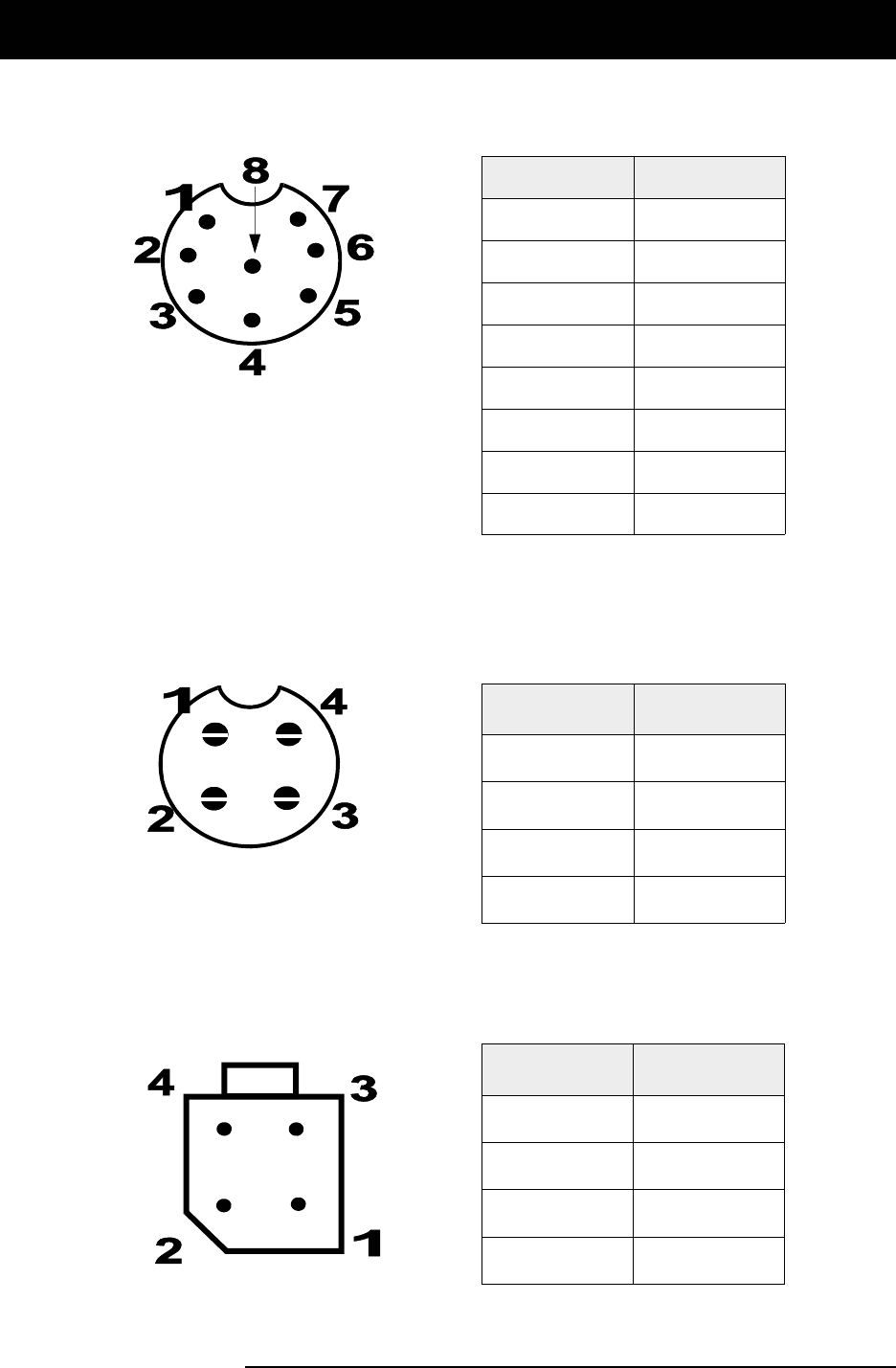
- 82 -
18. EXTERNAL CONNECTORS
Microphone connector (front panel)
Power connector (rear panel)
Pin No. Function
1 Microphone 1
2 Transmit data
3 Receive data
4 Loud speaker
5 Press to talk
6 Ground
7 Microphone 2
8 +5volt
Pin No. Function
1 Ground
2 Loud speaker
3 Aux. power
4 +12 to +28volt
The illustration above
shows the pin numbers on
the rear panel power
The illustration above
shows the pin numbers on
the front panel microphone
(viewed into front of connector)
(viewed into front of connector)
Loudspeaker receptacle (on cable)
(viewed looking into pins)
Pin No. Function
1 Ground
2 Aux Power
3 Loud Speaker
4 +12 to +28volt

- 83 -
19. DEVICE PINOUTS & CODES
Please refer to the following page for device pinouts & codes .....

- 84 -
REFER DEVICE PINOUTS DIAGRAM
IN FILE NAMED “QMACPINS.xxx”

- 85 -
19.1 SMD capacitor codes
Marking Value
A0 1p
N0 3p3
A1 10p
N1 33p
A2 100p
N2 330p
A3 1n
N3 3n3
A4 10n
N4 33n
A5 100n
N5 330n

- 86 -
Q-MAC Electronics Pty Ltd
(ABN 89054566684)
PO Box 1334, Osborne Park Business Centre, Western Australia 6916