Qisda GW50 MOD-SM Qisda BT/WLAN CWM-01 User Manual
Qisda Corporation MOD-SM Qisda BT/WLAN CWM-01
UserManual.wiki
>
Qisda
>
GW50 User Manual
user manual rev
Navigation menu
Upload a User Manual
Namespaces
Wiki Guide
HTML
PDF
Info
Views
User Manual
Discussion / Help
Navigation
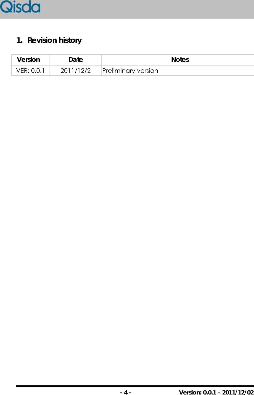
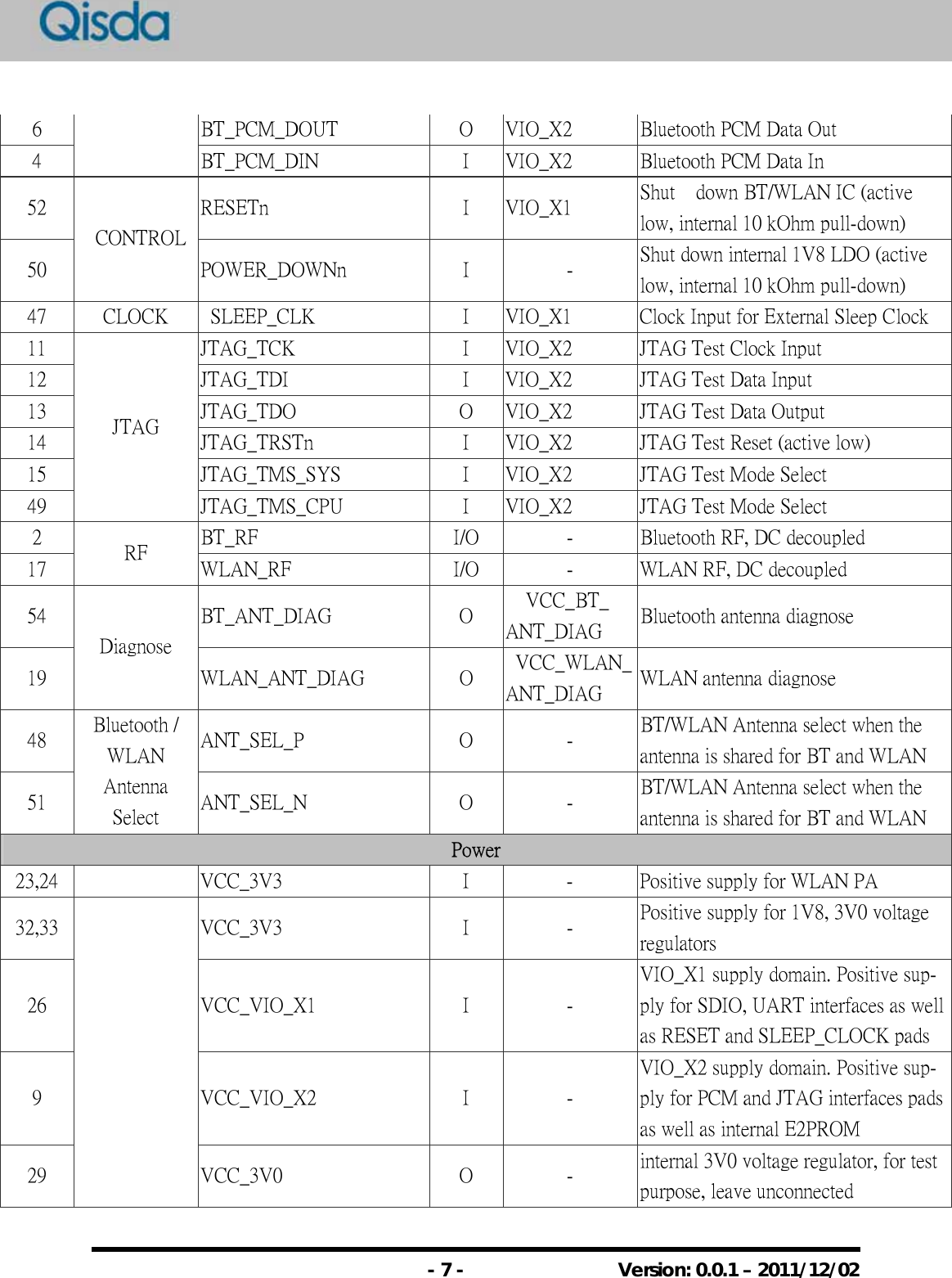
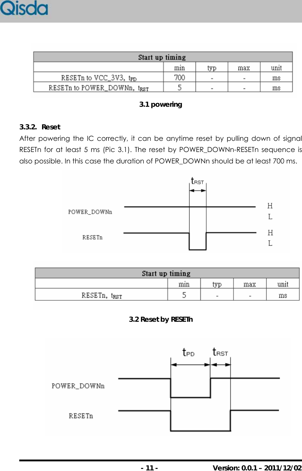
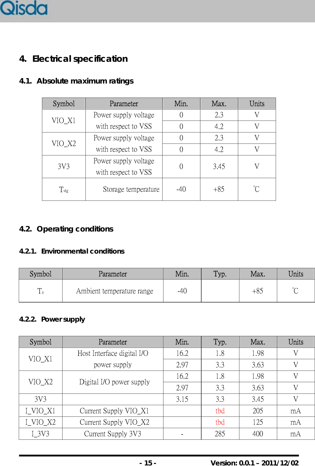
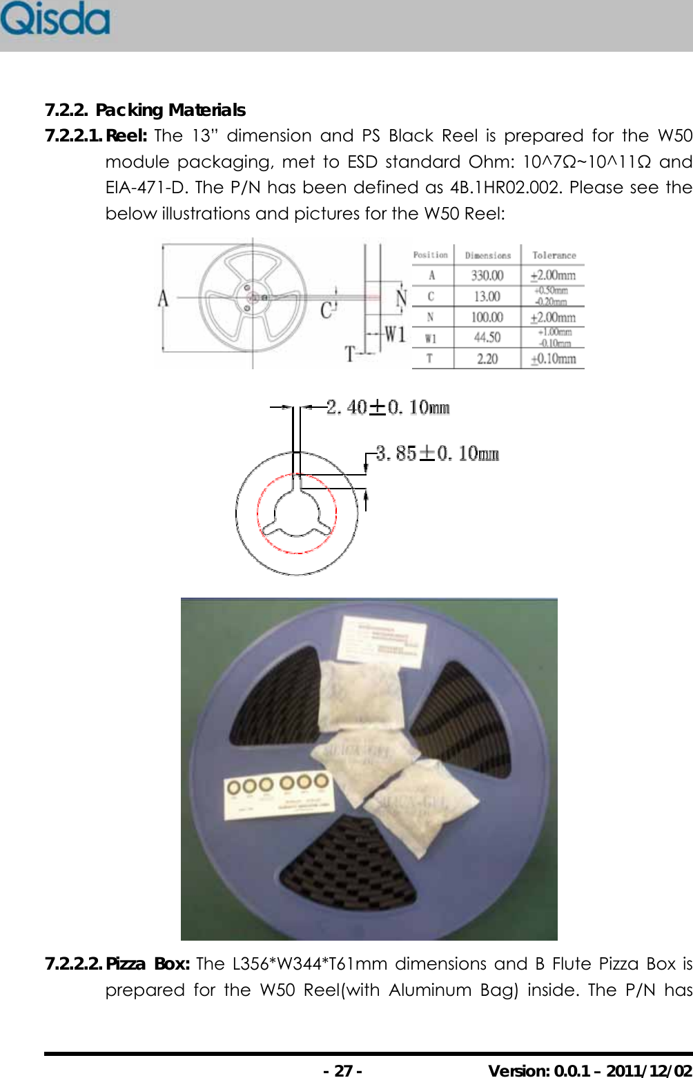
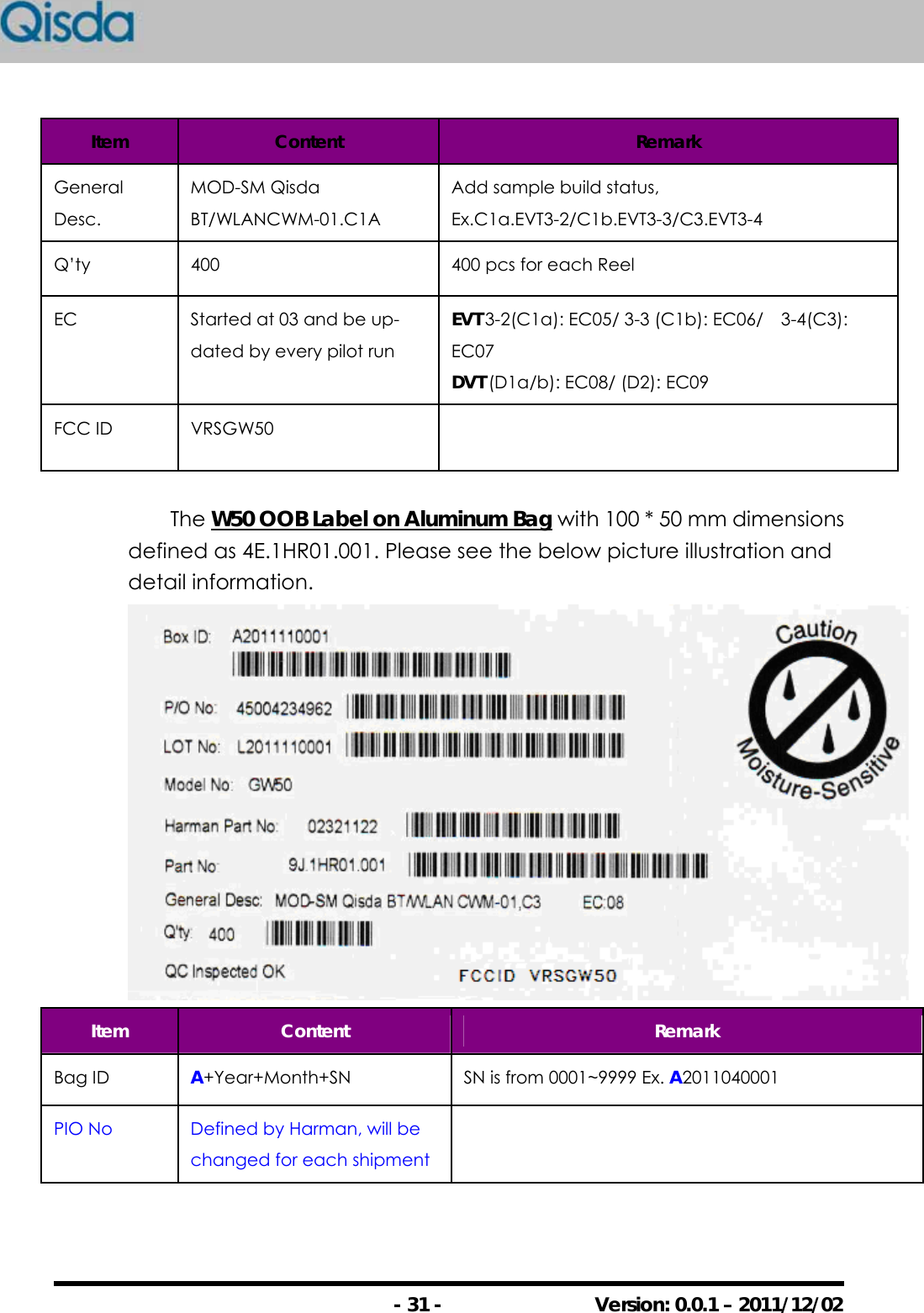
![- 6 - Version: 0.0.1 – 2011/12/02 2.2. Pin Configuration 2.2.1. Pin arrangement 1510 15 1845 40 35 30 2854504619252720GNDBT_RFGNDBT_PCM_DINBT_PCM_CLKBT_PCM_DOUTBT_PCM_SYNCGNDVCC_VIO_X2GNDJTAG _TCKJTAG_TDIJTAG_TDOJTAG_TRSTnJTAG_TMS_SYSGNDGNDWLAN_RFWLAN_ANT_DIAGVCC_WLAN_ANT_DIAGGNDGNDVCC_3V3VCC_3V3GNDGNDVCC_VIO_X1UART_TXUART_RXUART_RTSGNDSD_DATA[2]SD_DATA[3]SD_DATA[0]SD_DATA[1]SD_CMDSD_CLKGNDVCC_1V8VCC_3V3VCC_3V3GNDGNDVCC_3V0GNDUART_CTSSLEEP_CLKANT_SEL_PJTAG_TMS_CPUPOWER_DOWNnANT_SEL_NRSESTnVCC_BT_ANT_DIAGBT_ANT_DIAG Figure 2: Pin arrangement 2.2.2. Pin function Pin# Interface Pin Name Type Supply Description 36 SD_CLK I VIO_X1 SDIO Clock Input 37 SD_CMD I/O VIO_X1 SDIO Command 39 SD_DATA[0] I/O VIO_X1 SDIO Data Line Bit [0] 38 SD_DATA[1] I/O VIO_X1 SDIO Data Line Bit [1] 41 SD_DATA[2] I/O VIO_X1 SDIO Data Line Bit [2] 40 SDIO SD_DATA[3] I/O VIO_X1 SDIO Data Line Bit [3] 46 UART CTS I VIO_X1 UART Clear to send 44 UART RX I VIO_X1 UART Receive 45 UART TX O VIO_X1 UART Transmit 43 UART UART RTS O VIO_X1 UART Request to send 5 BT_PCM_CLK O VIO_X2 Bluetooth PCM Clock (master) 7 PCM BT_PCM_SYNC O VIO_X2 Bluetooth PCM Sync (master)](https://usermanual.wiki/Qisda/GW50/User-Guide-1651217-Page-6.png)