Qisda GW50 MOD-SM Qisda BT/WLAN CWM-01 User Manual
Qisda Corporation MOD-SM Qisda BT/WLAN CWM-01
Qisda >
user manual rev

Copyright ©2008 Qisda Corporation. Confidential Property
W50
WLAN / Bluetooth Wireless Module
Rev. 1.0.0
2011/10/20
Copyright © 2010 Qisda Corporation. All rights reserved.
This document contains proprietary technical information which is the property of Qisda
Corporation and is issued in strict confidential and shall not be disclosed to others parties in
whole or in parts without written permission of Qisda Corporation.
The documents contain information on a product, which is under development and is issued
for customer evaluation purposes only.
Qisda may make changes to product specifications at any time, without notice.
Wireless Data Application BD
Mobile Communications BU
Qisda Corporation
18 Jihu Road, Nei-Hu, Taipei 114, Taiwan
Tel: +886-2-2799-8800
Fax: +886-2-2656-6398
http://Qisda.com

- 2 - Version: 0.0.1 – 2011/12/02
Contents
1. REVISION HISTORY.............................................................................................4
2. FUNCTIONAL DESCRIPTION...............................................................................5
2.1. OVERVIEW.......................................................................................................................................5
2.2. PIN CONFIGURATION .......................................................................................................................6
2.2.1. PIN ARRANGEMENT ..........................................................................................................................6
2.2.2. PIN FUNCTION ..................................................................................................................................6
3. TECHNICAL DESCRIPTION..................................................................................9
3.1. RADIO FEATURES ..............................................................................................................................9
3.1.1. RF PORT...........................................................................................................................................9
3.1.2. RF BLUETOOTH.................................................................................................................................9
3.1.3. RF WLAN .......................................................................................................................................9
3.1.4. SPURIOUS EMISSIONS ........................................................................................................................9
3.2. CLOCK ............................................................................................................................................9
3.2.1. MAIN CLOCK .................................................................................................................................10
3.2.2. SLEEP CLOCK .................................................................................................................................10
3.3. START UP AND RESET.......................................................................................................................10
3.3.1. POWERING.....................................................................................................................................10
3.3.2. RESET .............................................................................................................................................11
3.4. ANTENNA DIAGNOSE CIRCUIT ........................................................................................................12
3.5. POWER SUPPLY...............................................................................................................................13
3.5.1. MAIN POWER.................................................................................................................................13
3.5.2. SUPPLY OF I/O PINS .......................................................................................................................14
3.5.3. POWER DOWN MODE ...................................................................................................................14
4. ELECTRICAL SPECIFICATION............................................................................15
4.1. ABSOLUTE MAXIMUM RATINGS........................................................................................................15
4.2. OPERATING CONDITIONS ...............................................................................................................15
4.2.1. ENVIRONMENTAL CONDITIONS .......................................................................................................15
4.2.2. POWER SUPPLY...............................................................................................................................15
4.2.3. DIGITAL PINS ..................................................................................................................................16
4.2.4. EXTERNAL SLEEP CLOCK TIMING.....................................................................................................16

- 3 - Version: 0.0.1 – 2011/12/02
4.2.5. RF PERFORMANCE ........................................................................................................................16
5. MECHANICAL SPECIFICATION........................................................................18
5.1. PACKAGE TYPE ..............................................................................................................................18
5.2. PACKAGE DIMENSIONS ..................................................................................................................18
6. LABELING AND ORDERING INFORMATION ....................................................20
6.1. PRODUCT LABEL .............................................................................................................................20
6.1.1. SHIELDING FRAME COVER LABEL ...................................................................................................20
6.1.2. SHIELDING CASE COVER LABEL .....................................................................................................20
6.2. ORDERING INFORMATION ..............................................................................................................21
7. PRODUCT HANDLING ......................................................................................21
7.1. PACKAGING ..................................................................................................................................21
7.2. PACKING MATERIALS .....................................................................................................................24
7.2.1. HUMIDITY PROTECTION MATERIALS ................................................................................................24
7.2.1.1. ALUMINUM BAG ...........................................................................................................................24
7.2.1.2.HUMIDITY INDICATOR ...........................................................................................................................25
7.2.1.3.DESICCANT ..........................................................................................................................................26
7.2.2. PACKING MATERIALS .....................................................................................................................27
7.2.2.1. REEL...............................................................................................................................................27
7.2.2.2. PIZZA BOX......................................................................................................................................27
7.2.2.3. CARTON ........................................................................................................................................29
7.2.3. LABELS ...........................................................................................................................................29
7.2.3.1. OOB LABEL...................................................................................................................................29
7.2.3.2. CARTON LABEL ..............................................................................................................................35
7.2.3.3. CAUTION LABEL .............................................................................................................................35
7.2.4. TAPES .............................................................................................................................................36
7.3. SHIPMENT, STORAGE AND HANDLING .............................................................................................37
8. CERTIFICATIONS...............................................................................................37
8.1. FCC REGULATIONS: .........................................................................................37
9. CONTACT.........................................................................................................38

- 4 - Version: 0.0.1 – 2011/12/02
1. Revision history
Version Date Notes
VER: 0.0.1 2011/12/2 Preliminary version

- 5 - Version: 0.0.1 – 2011/12/02
2. Functional description
2.1. Overview
This chapter provides a short overview over the most important functions and fea-
tures of the module. This data sheet is preliminary and will be changed if needed.
The module is built on the Marvell® 88W8688 low-cost highly-integrated IEEE
802.11a/g/b MAC/Baseband/RF WLAN and Bluetooth Baseband/RF system-on-chip
(SoC).
The module supports IEEE 802.11g payload data rates of 6, 9, 12, 18, 24, 36, 48, and 54
Mbps, as well as 802.11b data rates of 1, 2, 5.5 and 11 Mbps for WLAN operation.
For Bluetooth operation, the module supports Bluetooth 3.0 + High Speed (HS) (also
compliant with Bluetooth 2.1 + EDR).
For security, the 88W8688 supports the IEEE 802.11i security standard through imple-
mentation of the Advanced Encryption Standard (AES)/Counter Mode CBC-MAC
Protocol (CCMP), and Wired Equivalent Privacy (WEP) with Temporal Key Integrity
Protocol (TKIP) security mechanisms. The module also supports Internet Protocol Se-
curity (IPsec) with DES//3DES/AES encryption and MD5/SHA-1 authentication as well
as 802.11e Quality of Service (QoS).
The module supports dual SDIO host interface for connecting the WLAN and Blue-
tooth to the host processor. For Bluetooth application the high-speed UART (up to
4MB/s), PCM/Inter-IC Sound (I2S), are supported too.
For better throughput of WLAN/BT, the module provides different RF paths for WLAN
and Bluetooth for own antennas. By using of two antennas with enough decoupling it
enables to do without coexistence.
- 6 - Version: 0.0.1 – 2011/12/02
2.2. Pin Configuration
2.2.1. Pin arrangement
1510 15 18
45 40 35 30 28
54
50
46
19
25
27
20
GND
BT_RF
GND
BT_PCM_DIN
BT_PCM_CLK
BT_PCM_DOUT
BT_PCM_SYNC
GND
VCC_VIO_X2
GND
JTAG _TCK
JTAG_TDI
JTAG_TDO
JTAG_TRSTn
JTAG_TMS_SYS
GND
GND
WLAN_RF
WLAN_ANT_DIAG
VCC_WLAN_ANT_DIAG
GND
GND
VCC_3V3
VCC_3V3
GND
GND
VCC_VIO_X1
UART_TX
UART_RX
UART_RTS
GND
SD_DATA[2]
SD_DATA[3]
SD_DATA[0]
SD_DATA[1]
SD_CMD
SD_CLK
GND
VCC_1V8
VCC_3V3
VCC_3V3
GND
GND
VCC_3V0
GND
UART_CTS
SLEEP_CLK
ANT_SEL_P
JTAG_TMS_CPU
POWER_DOWNn
ANT_SEL_N
RSESTn
VCC_BT_ANT_DIAG
BT_ANT_DIAG
Figure 2: Pin arrangement
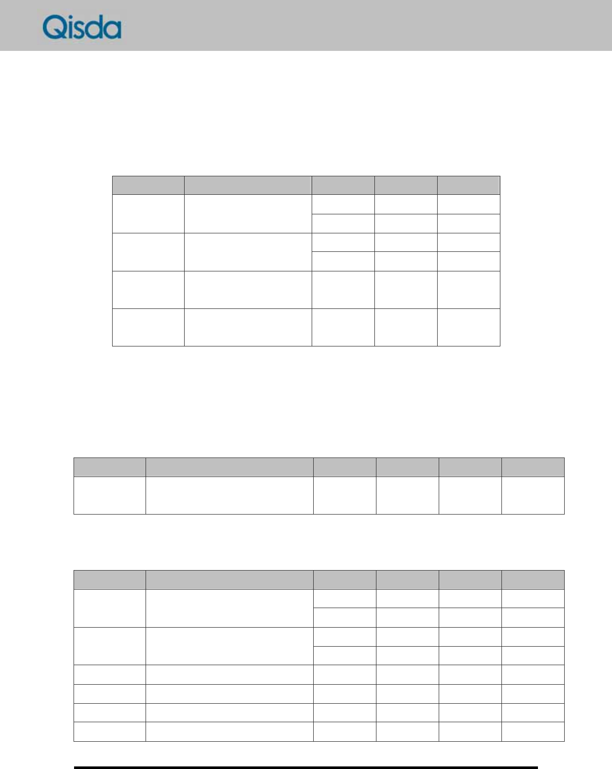
2.2.2. Pin function
Pin# Interface Pin Name Type Supply Description
36 SD_CLK I VIO_X1 SDIO Clock Input
37 SD_CMD I/O VIO_X1 SDIO Command
39 SD_DATA[0] I/O VIO_X1 SDIO Data Line Bit [0]
38 SD_DATA[1] I/O VIO_X1 SDIO Data Line Bit [1]
41 SD_DATA[2] I/O VIO_X1 SDIO Data Line Bit [2]
40
SDIO
SD_DATA[3] I/O VIO_X1 SDIO Data Line Bit [3]
46 UART CTS I VIO_X1 UART Clear to send
44 UART RX I VIO_X1 UART Receive
45 UART TX O VIO_X1 UART Transmit
43
UART
UART RTS O VIO_X1 UART Request to send
5 BT_PCM_CLK O VIO_X2 Bluetooth PCM Clock (master)
7
PCM
BT_PCM_SYNC O VIO_X2 Bluetooth PCM Sync (master)
- 7 - Version: 0.0.1 – 2011/12/02
6 BT_PCM_DOUT O VIO_X2 Bluetooth PCM Data Out
4
BT_PCM_DIN I VIO_X2 Bluetooth PCM Data In
52 RESETn I VIO_X1 Shut down BT/WLAN IC (active
low, internal 10 kOhm pull-down)
50
CONTROL
POWER_DOWNn I - Shut down internal 1V8 LDO (active
low, internal 10 kOhm pull-down)
47 CLOCK SLEEP_CLK I VIO_X1 Clock Input for External Sleep Clock
11 JTAG_TCK I VIO_X2 JTAG Test Clock Input
12 JTAG_TDI I VIO_X2 JTAG Test Data Input
13 JTAG_TDO O VIO_X2 JTAG Test Data Output
14 JTAG_TRSTn I VIO_X2 JTAG Test Reset (active low)
15 JTAG_TMS_SYS I VIO_X2 JTAG Test Mode Select
49
JTAG
JTAG_TMS_CPU I VIO_X2 JTAG Test Mode Select
2 BT_RF I/O - Bluetooth RF, DC decoupled
17 RF WLAN_RF I/O - WLAN RF, DC decoupled
54 BT_ANT_DIAG O VCC_BT_
ANT_DIAG Bluetooth antenna diagnose
19
Diagnose
WLAN_ANT_DIAG O VCC_WLAN_
ANT_DIAG WLAN antenna diagnose
48 ANT_SEL_P O - BT/WLAN Antenna select when the
antenna is shared for BT and WLAN
51
Bluetooth /
WLAN
Antenna
Select ANT_SEL_N O - BT/WLAN Antenna select when the
antenna is shared for BT and WLAN
Power
23,24 VCC_3V3 I - Positive supply for WLAN PA
32,33 VCC_3V3 I - Positive supply for 1V8, 3V0 voltage
regulators
26 VCC_VIO_X1 I -
VIO_X1 supply domain. Positive sup-
ply for SDIO, UART interfaces as well
as RESET and SLEEP_CLOCK pads
9 VCC_VIO_X2 I -
VIO_X2 supply domain. Positive sup-
ply for PCM and JTAG interfaces pads
as well as internal E2PROM
29
VCC_3V0 O - internal 3V0 voltage regulator, for test
purpose, leave unconnected
- 8 - Version: 0.0.1 – 2011/12/02
34 VCC_1V8 O - internal 1V8 voltage regulator, for test
purpose, leave unconnected
53 VCC_BT_ANT_DIAG I - Supply for BT antenna diagnose circuit
20 VCC_WLAN_ANT_DIAG I - Supply for WLAN antenna diagnose
circuit
1,3,8,
10,16,
18,21,
22,25,
27,28,
30,31,
35,42
GND - - Ground
*) The antenna diagnose functionality is supported only when antenna has a DC path with
51K Ohm resistance to ground.

- 9 - Version: 0.0.1 – 2011/12/02
3. Technical Description
3.1. Radio Features
3.1.1. RF port
For WLAN and Bluetooth, the module provides single ended, 50 ohm matched bidi-
rectional ports. The RX / TX switches are incorporated either in module or in 88W8688
chip.
3.1.2. RF Bluetooth
The RF part of Bluetooth has a balun for transforming the differential RF port of
88W8688 to single ended port of module. The balun is also used for powering internal
PA / LNA with 1, 8V supply.
The output power of 2 dBm with power control is fully compliant to BT Class II re-
quirements.
The RF modem supports GFSK and DPSK modulations according to Bluetooth 2.1+EDR
standard.
3.1.3. RF WLAN
The module supports 802.11g/b operation in word harmonized 2.4 GHz ISM band. The
Power Amplifier, RX balun and TX/RX switch are integrated in to module. The output
power is 15 +/- 1 dBm in automotive temperature range.
3.1.4. Spurious emissions
Both the spurious emission of conducted and radiated had compliant with the
standards EN 300328, FCC Part 15.247.
3.2. Clock
- 10 - Version: 0.0.1 – 2011/12/02
3.2.1. Main clock
The local oscillator and digital clocks are generated from crystal. The crystal is tuned
during production process and tune values are stored in on board E2PROM.
3.2.2. Sleep clock
The sleep clock is delivered from a external 32 kHz oscillator. This clock as from ex-
ternal source is required for Bluetooth low power mode applications.
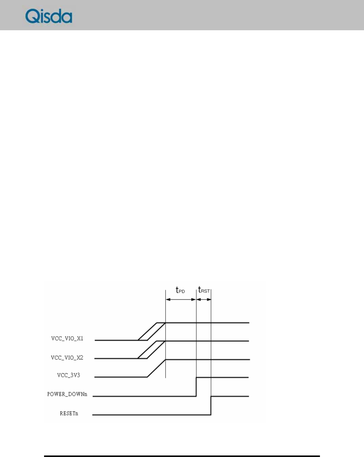
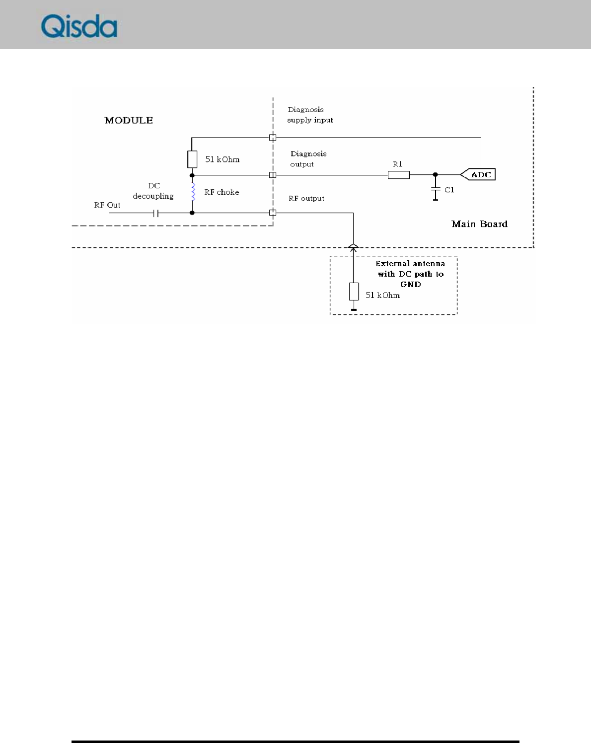
3.3. Start up and Reset
A low level at POWER_DOWNn pin turns off internal 1V8 LDO, but 3V0 band gap ref-
erence remain on. A low level at RESETn pin turns off IC, this pin is also used for basic
reset operation.
The both pins POWER_DOWNn and RESETn have internal 10K Ohm pull-down resistors.
It is distinguished between powering and reset.
3.3.1. Powering
While powering external voltages VCC_VIO_X1/2 VCC_3V3 are turned on. For cor-
rect functionality the start-up timing below has to follow. An additional reset isn’t
necessary. The VCC_VIO_X1 and X2 can be turned on before VCC_3V3 but latest
concurrently with it. The time between rising of VCC_VIO_X1/2 and VCC_3V3 isn’t
specified and can be unrestricted.
- 11 - Version: 0.0.1 – 2011/12/02
3.1 powering
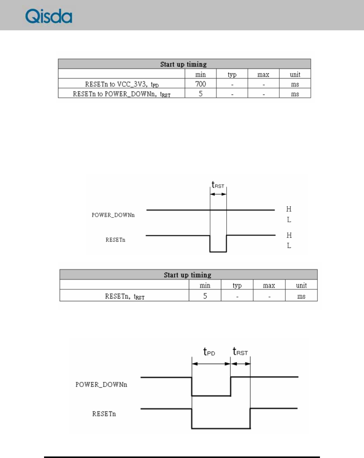
3.3.2. Reset
After powering the IC correctly, it can be anytime reset by pulling down of signal
RESETn for at least 5 ms (Pic 3.1). The reset by POWER_DOWNn-RESETn sequence is
also possible. In this case the duration of POWER_DOWNn should be at least 700 ms.
3.2 Reset by RESETn
- 12 - Version: 0.0.1 – 2011/12/02
3.3 Reset by RESETn and POWER_DOWNn
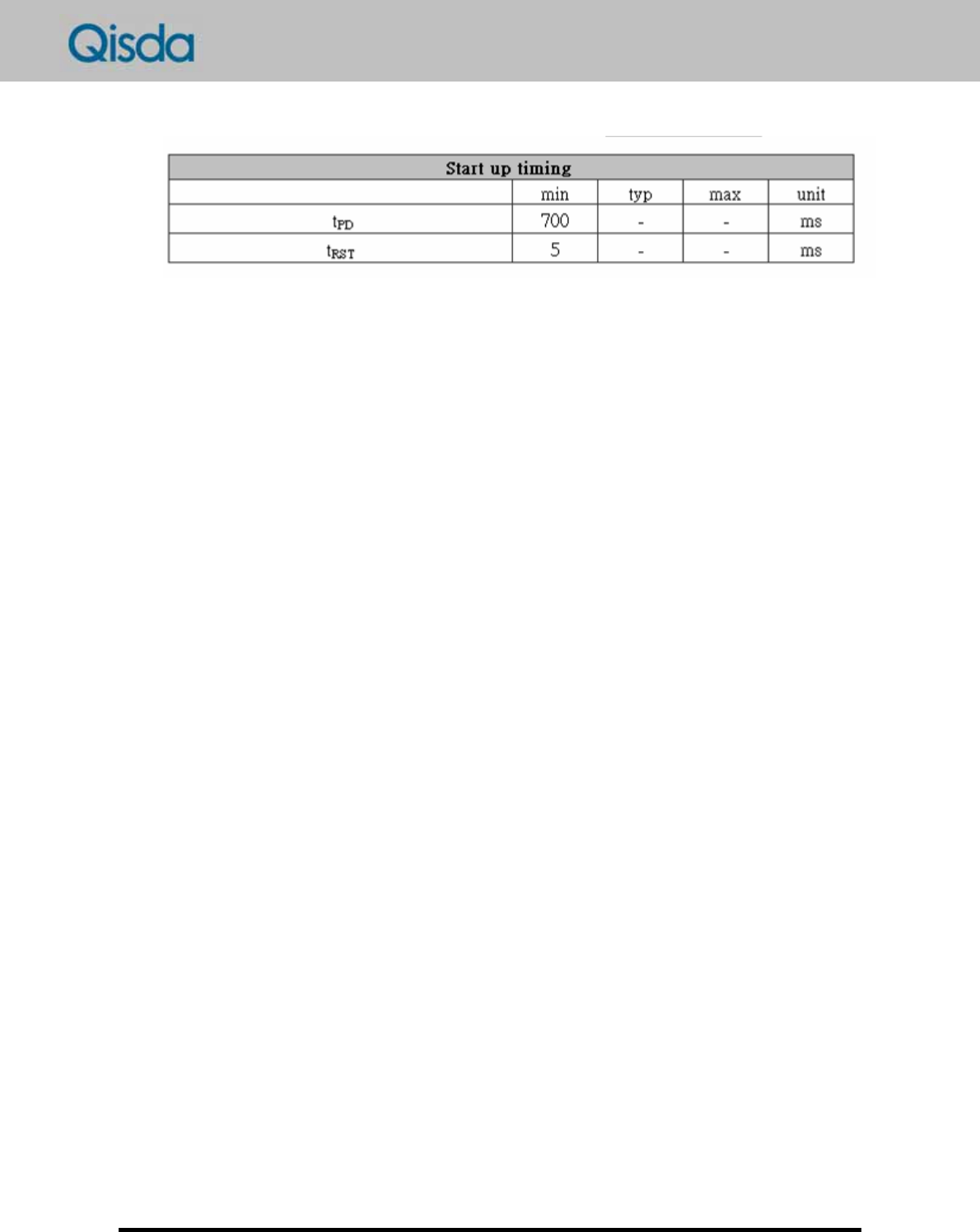
3.4. Antenna diagnose circuit
The picture below shows the principle of antenna diagnose circuit.
Requirement for functionality of circuit is that the external antenna has a internal DC
path to ground with real impedance value of 51K Ohm.
This impedance builds with in module built-in resistor of 51K Ohm a voltage divider. By
measuring and evaluation of voltage in divider midpoint it is possible to detected 3
states of antenna connection:
- open, measured voltage is equal supply voltage of antenna diagnose circuit
- antenna is connected correctly, measured voltage is equal the half of supply
voltage antenna diagnose circuit
- Antenna is shorted to GND, measured voltage is equal 0V
Those three states are detected if supply voltage of antenna diagnose circuit (pins
VCC_BT_ANT_DIAG or VCC_WLAN_ANT_DIAG) is equal reference voltage of ADC.
In case that supply voltage is lower than ADC reference voltage it is possible to de-
tect one more state:
- Antenna has bypass to higher voltage source (for example to UBAT), the
measured voltage is higher than supply voltage of antenna diagnose circuit.
On system side can be used a low pass filter for filtering. Good results can be
achieved when C1=220nF and R1=51K Ohm, in this case the resistor R1 limits the
current into ADC if antenna connector is shorted to battery voltage too.
- 13 - Version: 0.0.1 – 2011/12/02
3.5. Power supply
3.5.1. Main power
All for functionality necessary power supplies are generated by into module inte-
grated 1.8 V LDO, 1V and 3.0 V band gap reference. The digital core supply of 1,2V is
generated by in 88W8688 integrated LDO powering external voltages VCC_VIO_X1/2
VCC_3V3 are turned on.
For correct functionality the start-up timing below has to follow. An additional reset
isn’t necessary. The VCC_VIO_X1 and X2 can be turned on before VCC_3V3 but lat-
est concurrently with it. The time between rising of VCC_VIO_X1/2 and VCC_3V3 isn’t
specified and can be unrestricted.
- 14 - Version: 0.0.1 – 2011/12/02
3.4 Power supply structure
3.5.2. Supply of I/O pins
The I/O pins are grouped in two supply domains: VCC_VIO_X1 and VCC_VIO_X2. Ba-
sically each domain can be powered either from 1,8V or 3,3V, but in circuits used
E2PROM can’t be powered by dual voltage. So supply of the VCC_VIO_X2 domain is
specified by E2PROM chip. The supply for VCC_VIO_X2 can be chosen at ordering.
The supply for VCC_VIO_X1 can be free chosen.
3.5.3. Power Down Mode
The module can be put into power down mode by signal POWER_DOWNn (Pin 50,
active level low).
Please note that 3V0 bang gap reference always remains on and consumes about
10 mA even if the IC and 1V8 LDO are powered down. From Power Down Mode the
module can be wacked up by powering sequence (pic. 3.1).
- 15 - Version: 0.0.1 – 2011/12/02
4. Electrical specification
4.1. Absolute maximum ratings
Symbol Parameter Min. Max. Units
0 2.3 V
VIO_X1 Power supply voltage
with respect to VSS 0 4.2 V
0 2.3 V
VIO_X2 Power supply voltage
with respect to VSS 0 4.2 V
3V3 Power supply voltage
with respect to VSS 0 3.45 V
Tstg Storage temperature -40 +85 ℃
4.2. Operating conditions
4.2.1. Environmental conditions
Symbol Parameter Min. Typ. Max. Units
Ta Ambient temperature range -40 +85 ℃
4.2.2. Power supply
Symbol Parameter Min. Typ. Max. Units
16.2 1.8 1.98 V
VIO_X1 Host Interface digital I/O
power supply 2.97 3.3 3.63 V
16.2 1.8 1.98 V
VIO_X2 Digital I/O power supply 2.97 3.3 3.63 V
3V3 3.15 3.3 3.45 V
I_VIO_X1 Current Supply VIO_X1 tbd 205 mA
I_VIO_X2 Current Supply VIO_X2 tbd 125 mA
I_3V3 Current Supply 3V3 - 285 400 mA
- 16 - Version: 0.0.1 – 2011/12/02
4.2.3. Digital pins
Symbol Parameter VCC_VIO Min. Typ. Max. Units
Power Down input, High - 1.4 - 5.5 V POWER_
DOWNn Power Down input, Low - -0.3 - 0.5 V
1.8 1.2 - V18+0.3 V
Vin Input high voltage 3.3 2.3 - V33+0.3 V
1.8 -0.3 - 0.6 V
Vin Input low voltage 3.3 -0.3 - 1.1 V
1.8 1.22 - - V
Vout Output high voltage 3.3 2.57 - - V
1.8 - - 0.4 V
Vout Output low voltage 3.3 - - 0.4 V
4.2.4. External Sleep Clock Timing
Symbol Parameter Min. Typ. Max. Units
CLK Clock Frequency
Range
32 or 32.768 - 50
ppm
32 or
32.768
32 or 32.768 + 50
ppm kHZ
THIGH Clock high time 40 -- -- ns
TLOW Clock low time 40 -- -- ns
TRISE Clock rise time -- -- 5 ns
TFALL Clock fall time -- -- 5 ns
4.2.5. RF Performance
4.2.5.1 BT Radio Characteristics
Parameter Items Specifications
Transmit Power Level
Class1.5:
7.8 ± 0.8 dBm (2441Mhz),
7.8 ± 1.5 dBm (2402~2480Mhz),
Class2.0:
2.5 ± 0.8 dBm (2441Mhz),
2.5 ± 1.5 dBm (2402~2480Mhz),
Receive Sensitivity -80dBm (GFSK),
-77dBm (π/4-DQPSK),
-77dBm (8DPSK)
Operating Frequency 2402 MHz to 2480 MHz
- 17 - Version: 0.0.1 – 2011/12/02
Parameter Items Specifications
Channel 79
Carrier Spacing 1 MHz separation
Duplexing Time Division Duplex
Hopping Rate 1600 hops/per second
Symbol Rate
1 Mbps (GFSK)
2 Mbps (π/4-DQPSK)
3 Mbps (8DPSK)
Modulation
GFSK BT =0.5
π/4-DQPSK
8DPSK
4.2.5.2 WLAN Radio Characteristics
Parameter Items Specifications
Frequency Band 2.4000~2.4835Ghz (2.4G ISM Band)
Selectable Sub Channel 13 Channels
(F=2412+n*5Mhz,n=0~12)
Modulation OFDM, DSSS (Direct Sequence Spread Spectrum), DBPSK,
DQPSK, CCK , 16QAM, 64QAM
Supported Rates 1, 2, 5.5, 11 Mbps (802.11b)
6, 9, 12, 18, 24, 36, 48, 54 Mbps (802.11g)
Maximum Receiver Level -10dBm with PER < 8% (802.11b)
-10dBm with PER < 10% (802.11g)
Output Power 15 dBm ± 1.5 dBm for 1, 2, 5.5, 11Mbps (802.11b)
15 dBm ± 1.5 dBm for 6 ,9 and >12Mhz (802.11g)
Carrier Frequency Accuracy +/- 25ppm
(+/-2ppm in 25℃)
802.11b Mode EVM
1.0 Mbps (BPSK) : <35%
2.0 Mbps (BPSK) : <35%
5.5 Mbps (QPSK) : <35%
11.0 Mbps (QPSK) : <35%
802.11g Mode EVM
6.0 Mbps (BPSK) : <-5.0dB
9.0 Mbps (BPSK) : <-8.0dB
12.0 Mbps (QPSK) : <-10.0dB
18.0 Mbps (QPSK) : <-13.0dB
24.0 Mbps (16-QAM) : <-16.0dB
36.0 Mbps (16-QAM) : <-19.0dB
48.0 Mbps (64-QAM) : <-22.0dB
54.0 Mbps (64-QAM) : <-25.0dB
802.11b Mode Sensitivity PER <8%, Rx Sensitivity @ 1.0 Mbps : -90dBm
PER <8%, Rx Sensitivity @ 11.0 Mbps: -86dBm
- 18 - Version: 0.0.1 – 2011/12/02
Parameter Items Specifications
802.11g Mode Sensitivity PER <10%, Rx Sensitivity @ 6.0 Mbps: -88dBm
PER <10%, Rx Sensitivity @ 54.0 Mbps: -72dBm
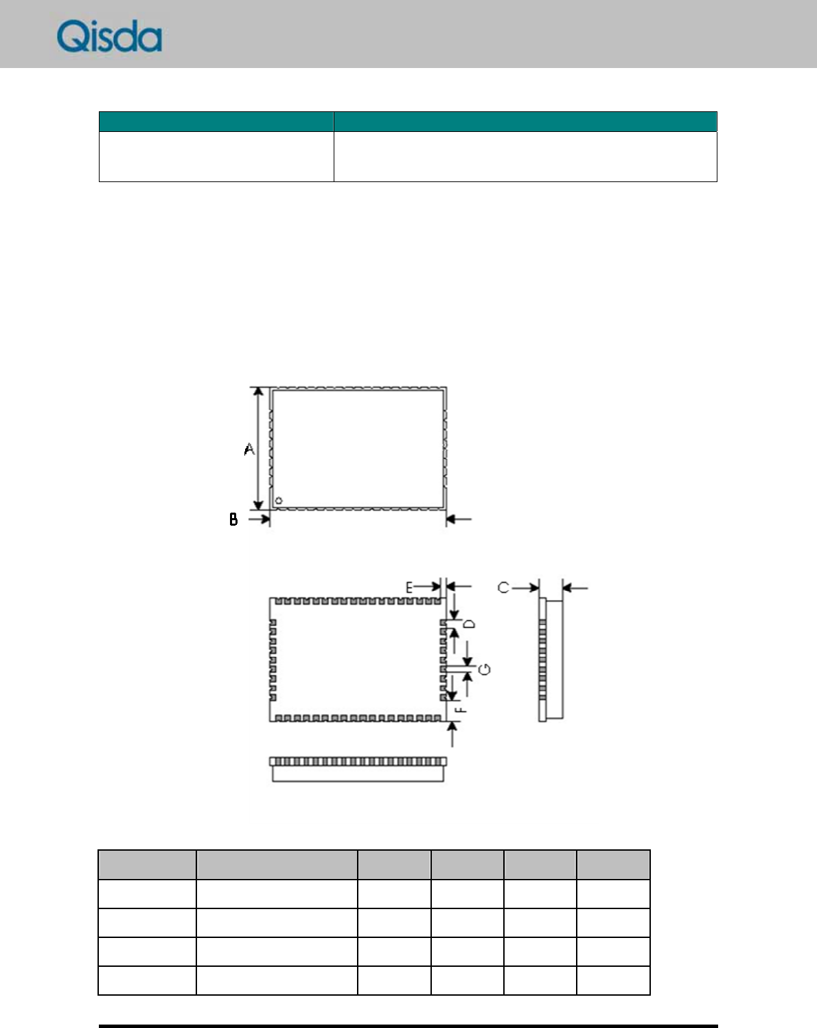
5. Mechanical specification
5.1. Package Type
54pin LGA, 1,6mm pitch
5.2. Package dimensions
Figure 3 : Package dimensions
Parameter Description Min. Typ. Max. Units
A Height 0.15 21 0.15 mm
B Width 0.15 30 0.3 mm
C Thickness 0.2 4 0.15 mm
D Pin to Pin Pitch tbd 1.6 tbd mm
- 19 - Version: 0.0.1 – 2011/12/02
E Edge to Pin tbd 0.9 tbd mm
F Edge to Pin tbd 3.6 tbd mm
G Pin Width tbd 1 tbd mm
Weight 5 g
- 20 - Version: 0.0.1 – 2011/12/02
6. Labeling and ordering information
6.1. Product label
2 Product Labels of W50 have been placed on Shielding Frame and
Shielding Case. For more information about the W50 Product Labels, please
refer to the below 6.1.1 and 6.1.2.
6.1.1. Shielding Frame Cover Label
The Label type of W50 Shielding Frame cover label is a 2D-Code Label
with 9 * 9 mm dimensions. The P/N has been defined as 4E.1HR02.001. The
2D-Code digits have been defined as below:
1st digit: Present the 2D-Code type.
2nd digits: Present the Main board type.
3rd~4th digits: Present the Model type.
5th~6th digits: Present the Date. Refer to the below figure for the Date
code rules.
7th digit: Present the Factory code.
8th~12th digits: Present the serial number.
6.1.2. Shielding Case Cover Label
The W50 Shielding Case cover label with 13 * 13 mm dimensions, defined
as 4E.1HR01.001, included below information:
A. 2D-Barode: The digital definition refer to the below 2D Barcode Defini-
tion chart.
- 21 - Version: 0.0.1 – 2011/12/02
B. P/N: Present the Harman PCBA Part Number.
C. S/N: Present the Harman Serial Number.
D. EC: Present the Engineering Changer Number.
2D Barcode Definition (1/3)
xxx 1xxxxxxxx
xx 01 xxxxxxxx, LICHRG#
Desc.
Qisda
Supplier
Code
Harman
Serial
No.
EC
Level
Harman
Module No.
Harman
PCBA
Part. No.
Fixed Specified
Key
Digits 3 digits 9 digits 2 digits 2 digits 8 digits+1 7 digits
2D Barcode Definition (2/3)
YYYYMMDD,KD_PC# GW50, KD_SN# 9J1HR01001 S0x, MAC-ADR#
Supplier
Production
Date,
Fixed
Specified
Key
Qisda In-
ternal Pro-
ject No.
Fixed Speci-
fied Key
Qisda In-
ternal Part
No.
Qisda In-
ternal Ver-
sion No.
Fixed Spe-
cified Key
8 digits+1 6 digits 4 digits+1 6 digits 10 digits 3 digits+1 8 digits
2D Barcode Definition (3/3)
xxxxxxxxxxxx, BLUE-TOOTH# xxxxxxxxxxxx,
WiFi MAC, Fixed Specified Key BT MAC,
12 digits+1 11 digits 12 digits+1
6.2. Ordering information
Ordering No. Product
CWM-01-3V3 Bluetooth/WLAN Module 3,3V supply
7. Product handling
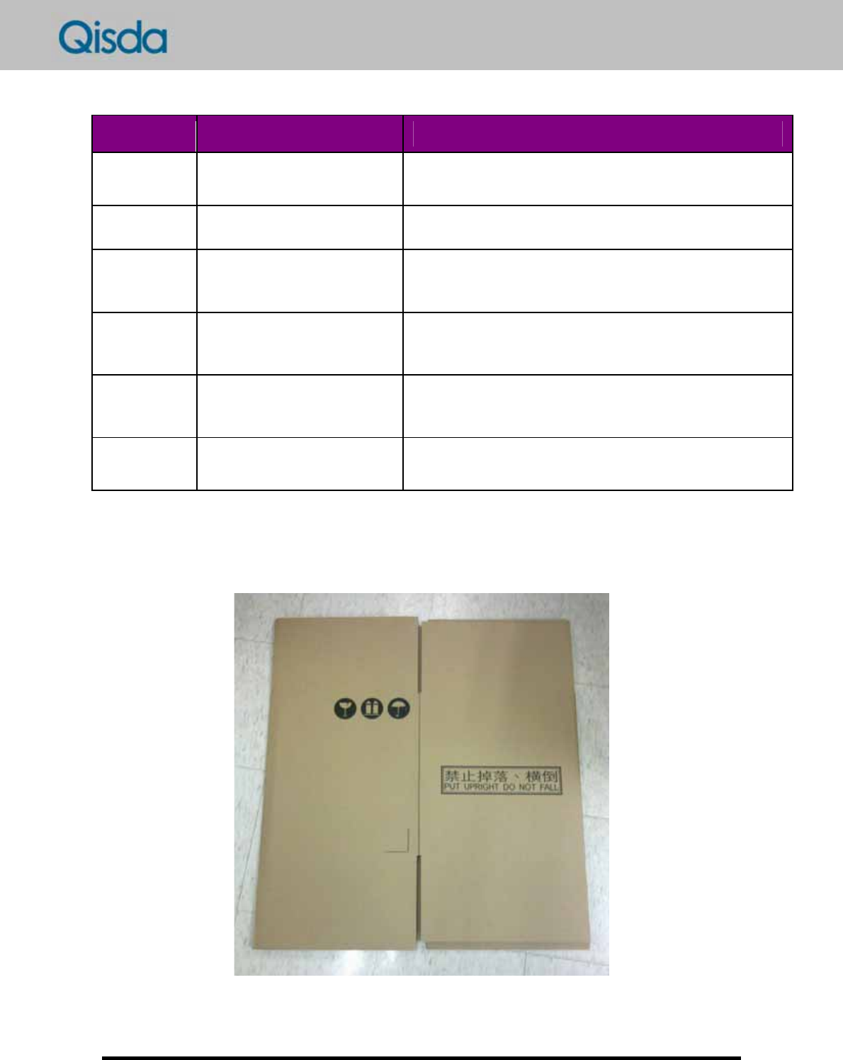
7.1. Packaging
Below Table 1 displays the W50 Packaging list, including Humidity Protec-
- 22 - Version: 0.0.1 – 2011/12/02
tion Materials, Packing Materials, Labels, and Taps. For more information
about the illustration of W50 packaging materials, please refer to the Figure 1
and Figure 2.
Table 1 W50 Packaging table
Type Item Spec. Qisda P/N Packaging
Figure No.
Aluminum
Bag
L460 * W410 * T0.15
mm
ALUMINUM BAG
GW50
4G.1HR01.00
1 8
Humidity In-
dicator
CARD HUMIDITY IN-
DICATOR GP 4J.G3501.002 9
1. Humid-
ity Pro-
tection
Materi-
als
DESICCANT
BAG
DESICCANT BAG
68*89 3H.09005.001 12
Taping Reel PLATE TAPING REEL
13IN. GW50 4B.1HR02.001 4
Pizza Box L356 * W344 * T61
mm 4D.1HR01.001 10
2. Pack-
ing
Materi-
als
Carton L355 * W340 * T386
mm (Pizza Box * 5) 4D.1HR02.001 1
OOB Label 100*50mm 4E.1HR03.001 2
Carton Label 50*15mm (Print on
Carton ) X 3
3. Labels
Caution
label
LABEL ATTENTION
56M31
55 mm * 55 mm
4E.G3503.001 11
Cover Tap COVER TAPE GW50 4B.1HR01.001 5
4. Taps
Carrier Tap CARRIER TAPE GW50 4B.1HR03.001 6
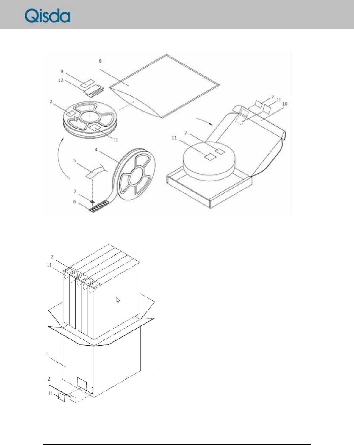
- 23 - Version: 0.0.1 – 2011/12/02
Figure 1 W50 Packaging 1/2
Figure 2 W50 Packaging 2/2
- 24 - Version: 0.0.1 – 2011/12/02
7.2. Packing Materials
7.2.1. Humidity Protection Materials
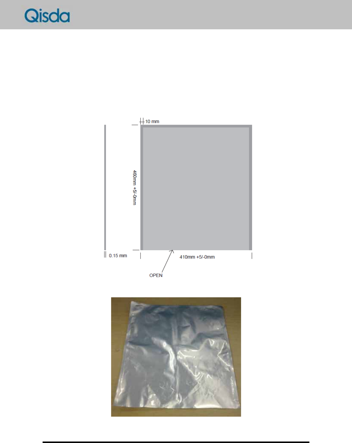
7.2.1.1. Aluminum Bag: The L460*W410*T0.15 mm dimensions Aluminum bag is
prepared for the W50 module vacuum packing on the Humidity pro-
tection purpose. The P/N has been defined as 4G.1HR01.001. Please
see the below illustration and picture for the W50 Aluminum bag:
- 25 - Version: 0.0.1 – 2011/12/02
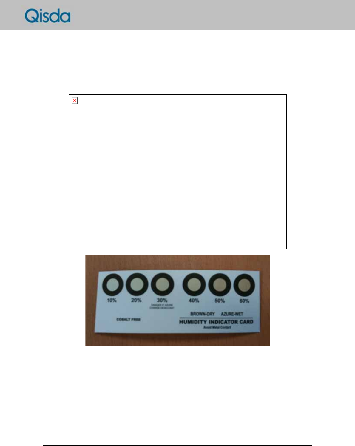
7.2.1.2. Humidity Indicator: The L102*W38 mm dimensions Humidity Indicator is
prepared for including in the W50 Aluminum Bag on the Humidity In-
spection purpose. The P/N has been defined as 4J.G3501.002. Please
see the below illustration and picture for the W50 Humidity Indicator:
湿
度卡
图
.jpg
- 26 - Version: 0.0.1 – 2011/12/02
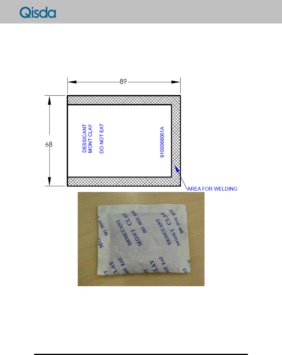
7.2.1.3. Desiccant: The L89*W68 mm dimensions and Mineral Bentonite inside
Desiccant is prepared for the W50 module packaging on the Humidity
prevention purpose. The P/N has been defined as 3H.09005.001. Please
see the below illustration and picture for the W50 Desiccant:
- 27 - Version: 0.0.1 – 2011/12/02
7.2.2. Packing Materials
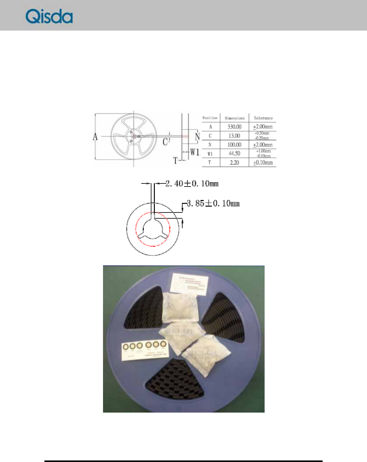
7.2.2.1. Reel: The 13” dimension and PS Black Reel is prepared for the W50
module packaging, met to ESD standard Ohm: 10^7Ω~10^11Ω and
EIA-471-D. The P/N has been defined as 4B.1HR02.002. Please see the
below illustrations and pictures for the W50 Reel:
7.2.2.2. Pizza Box: The L356*W344*T61mm dimensions and B Flute Pizza Box is
prepared for the W50 Reel(with Aluminum Bag) inside. The P/N has
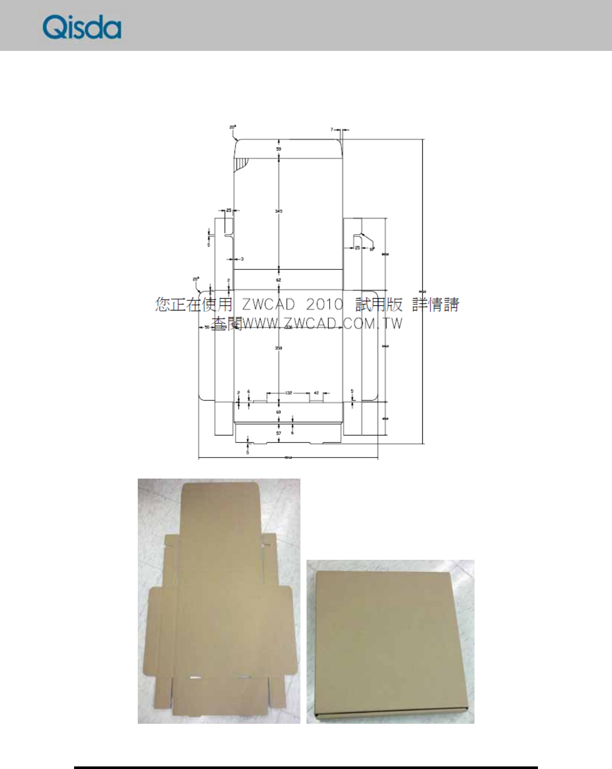
- 28 - Version: 0.0.1 – 2011/12/02
been defined as 4D.1HR01.001. Please see the below illustration and
pictures for the W50 Pizza Box:
- 29 - Version: 0.0.1 – 2011/12/02
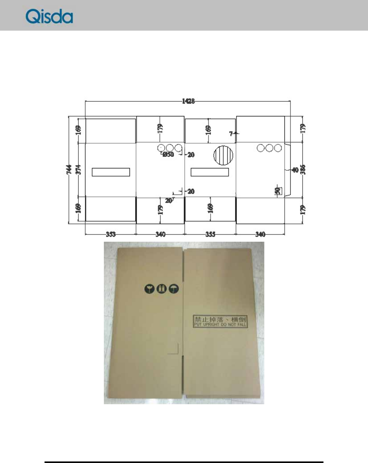
7.2.2.3. Carton: The L355*W340*T384mm dimensions and AB/F Carton is pre-
pared for the 5 Pizza Boxes inside. The P/N has been defined as
4D.1HR02.001. Please see the below illustration and picture for the W50
Carton:
7.2.3. Labels
7.2.3.1. OOB Label: 4 OOB Labels on Reel, Aluminum Bag, Pizza Box and Car-
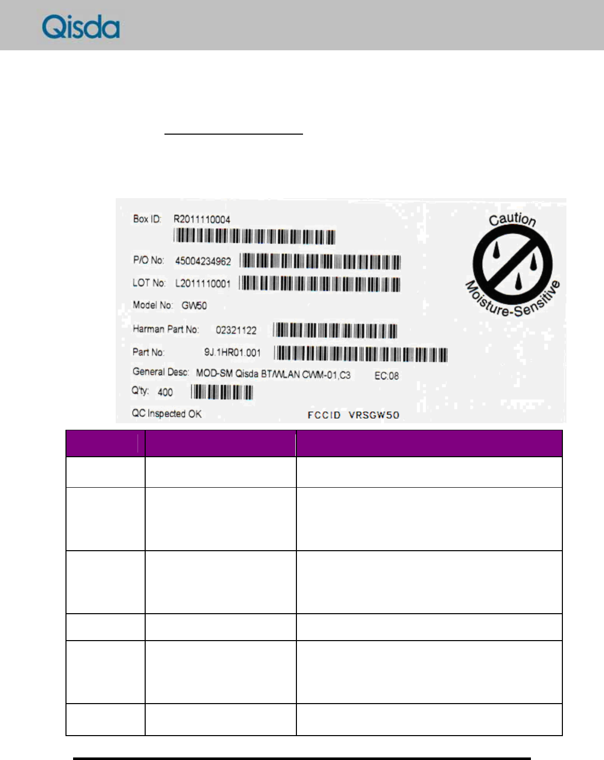
- 30 - Version: 0.0.1 – 2011/12/02
ton are placed for the W50. For more information about the W50 OOB
Labels, please refer to the below description.
The W50 OOB Label on Reel with 100 * 50 mm dimensions defined
as 4E.1HR01.001. Please see the below picture illustration and detail
information.
Item Content Remark
Reel ID R+Year+Month+SN SN is from 0001~9999 Ex. R2011040001
PIO No Defined by Harman, will be
changed for each ship-
ment
Lot No L+Year+month+SN (a) 5 Pizza boxes are in 1 Lot. (b) SN is from
0001~9999
Ex. L2011040001
Model No GW50 Qisda Model No.
Harman Part
No
Defined by Harman, will be
changed for each ship-
ment
C1b sample:2318091
C3/D1 sample:2321122
D2 sample : 2357720
Part No. 9J.1HR01.001 Qisda Part No.
- 31 - Version: 0.0.1 – 2011/12/02
Item Content Remark
General
Desc.
MOD-SM Qisda
BT/WLANCWM-01.C1A
Add sample build status,
Ex.C1a.EVT3-2/C1b.EVT3-3/C3.EVT3-4
Q’ty 400 400 pcs for each Reel
EC Started at 03 and be up-
dated by every pilot run
EVT 3-2(C1a): EC05/ 3-3 (C1b): EC06/ 3-4(C3):
EC07
DVT (D1a/b): EC08/ (D2): EC09
FCC ID VRSGW50
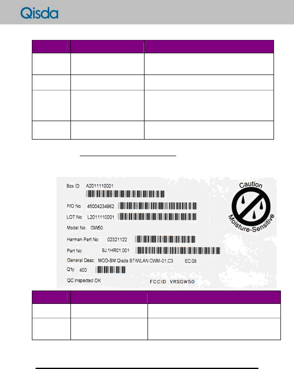
The W50 OOB Label on Aluminum Bag with 100 * 50 mm dimensions
defined as 4E.1HR01.001. Please see the below picture illustration and
detail information.
Item Content Remark
Bag ID A+Year+Month+SN SN is from 0001~9999 Ex. A2011040001
PIO No Defined by Harman, will be
changed for each shipment
- 32 - Version: 0.0.1 – 2011/12/02
Item Content Remark
Lot No L+Year+month+SN (a) 5 Pizza boxes are in 1 Lot. (b) SN is from
0001~9999
Ex. L2011040001
Model No GW50 Qisda Model No.
Harman Part
No
Defined by Harman, will be
changed for each shipment
C1b sample:2318091
C3/D1 sample:2321122
D2 sample :2357720
Part No. 9J.1HR01.001 Qisda Part No.
General
Desc.
MOD-SM Qisda
BT/WLANCWM-01.C1A
Add sample build status,
Ex.C1a.EVT3-2/C1b.EVT3-3/C3.EVT3-4
Q’ty 400 400 pcs for each Aluminum Bag
EC Started at 03 and be up-
dated by every pilot run
EVT 3-2(C1a): EC05/ 3-3 (C1b): EC06/ 3-4(C3): EC07
DVT (D1a/b): EC08/ (D2): EC09
FCC ID VRSGW50
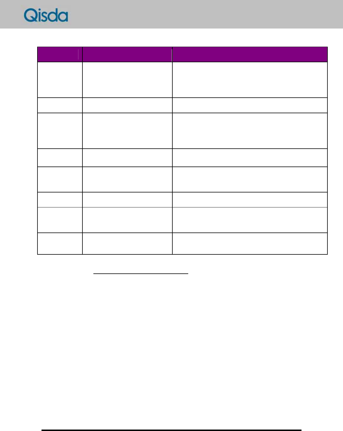
The W50 OOB Label on Pizza Box with 100 * 50 mm dimensions de-
fined as 4E.1HR01.001. Please see the below picture illustration and
detail information.
- 33 - Version: 0.0.1 – 2011/12/02
Item Content Remark
Box ID B+Year+Month+SN SN is from 0001~9999 Ex. B2011040001
PIO No Defined by Harman, will be
changed for each shipment
Lot No L+Year+month+SN (a) 5 Pizza boxes are in 1 Lot. (b) SN is from
0001~9999
Ex. L2011040001
Model No GW50 Qisda Model No.
Harman
Part No
Defined by Harman, will be
changed for each shipment
C1b sample:2318091
C3/D1 sample:2321122
D2 sample : 2357720
Part No. 9J.1HR01.001 Qisda Part No.
General
Desc.
MOD-SM Qisda
BT/WLANCWM-01.C1A
Add sample build status,
Ex.C1a.EVT3-2/C1b.EVT3-3/C3.EVT3-4
Q’ty 400 400 pcs for each Pizza Box
EC Started at 03 and be updated by
every pilot run
EVT 3-2(C1a): EC05/ 3-3 (C1b): EC06/ 3-4(C3):
EC07
- 34 - Version: 0.0.1 – 2011/12/02
Item Content Remark
DVT (D1a/b): EC08/ (D2): EC09
FCC ID VRSGW50
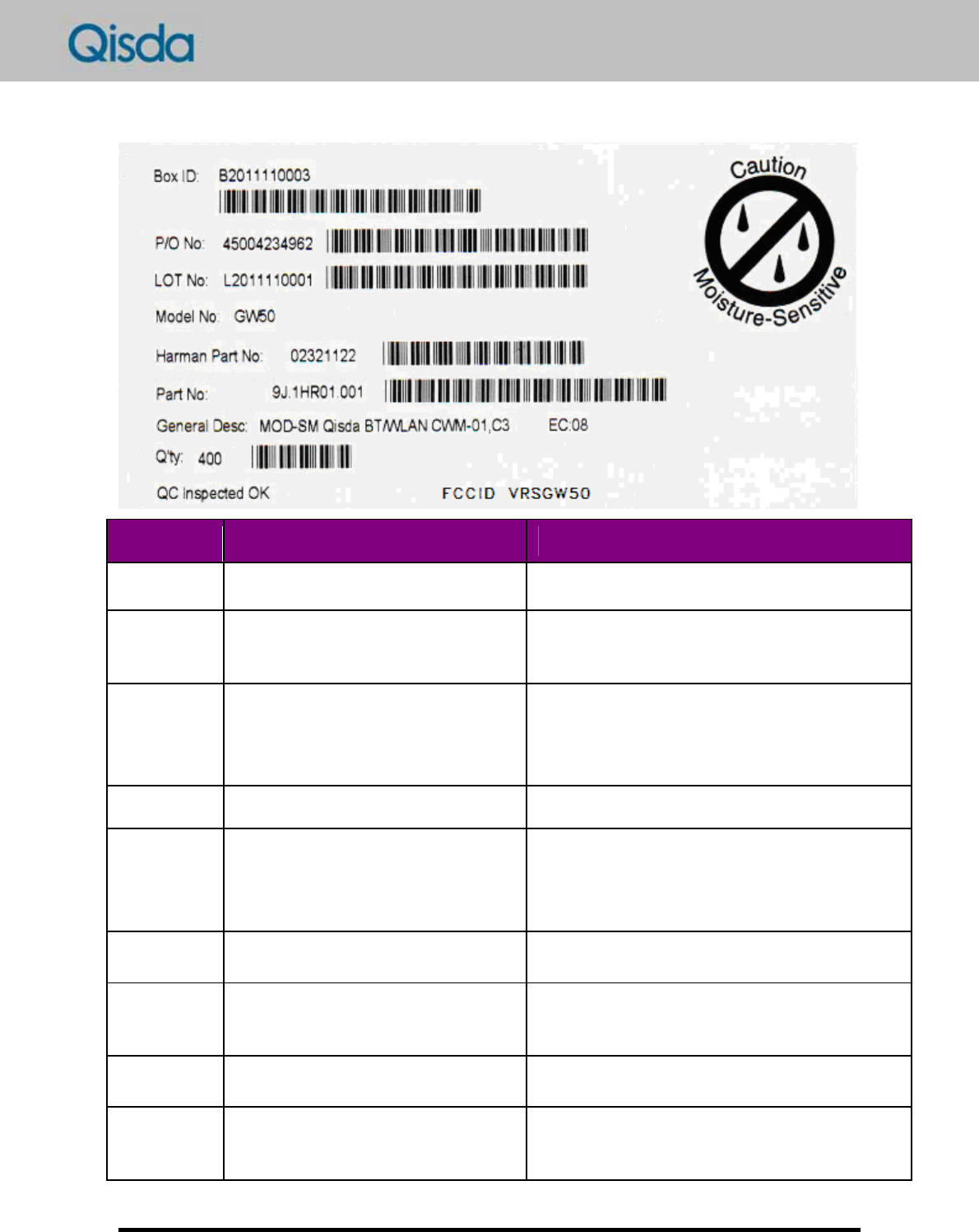
The W50 OOB Label on Carton with 100 * 50 mm dimensions de-
fined as 4E.1HR01.001. Please see the below picture illustration and
detail information.
Item Content Remark
Carton ID C+Year+Month+SN SN is from 0001~9999 Ex. C2011040001
PIO No Defined by Harman, will be
changed for each ship-
ment
Lot No L+Year+month+SN (a) 5 Pizza boxes are in 1 Lot. (b) SN is from
0001~9999
Model No GW50 Qisda Model Number
Harman
Part No
Defined by Harman, will be
chan
g
ed for each shi
p
-
(a) EVT3-3(C1b sample): 02318091
(b) EVT3-4(C3 /D1 sample): 02321122
- 35 - Version: 0.0.1 – 2011/12/02
Item Content Remark
ment (c ) D2 sample : 02357720
Part No. 9J.1HR01.001 Qisda Part Number
General
Desc.
MOD-SM Qisda BT/WLAN
CWM-01.CXX
Add sample build status as “XX”
Ex.C1A=EVT3-2/C1B=EVT3-3/ C3=EVT3-4
Q’ty Depend on shipment Q’ty 400 pcs for 1 Reel, Max Q’ty is 2000 pcs for each
Carton
EC Start from 03 and be up-
dated by every pilot run
EVT 3-2(C1a): EC05/ 3-3 (C1b): EC06/ 3-4(C3): EC07
DVT (D1a/b): EC08/ (D2): EC09
FCC ID VRSGW50
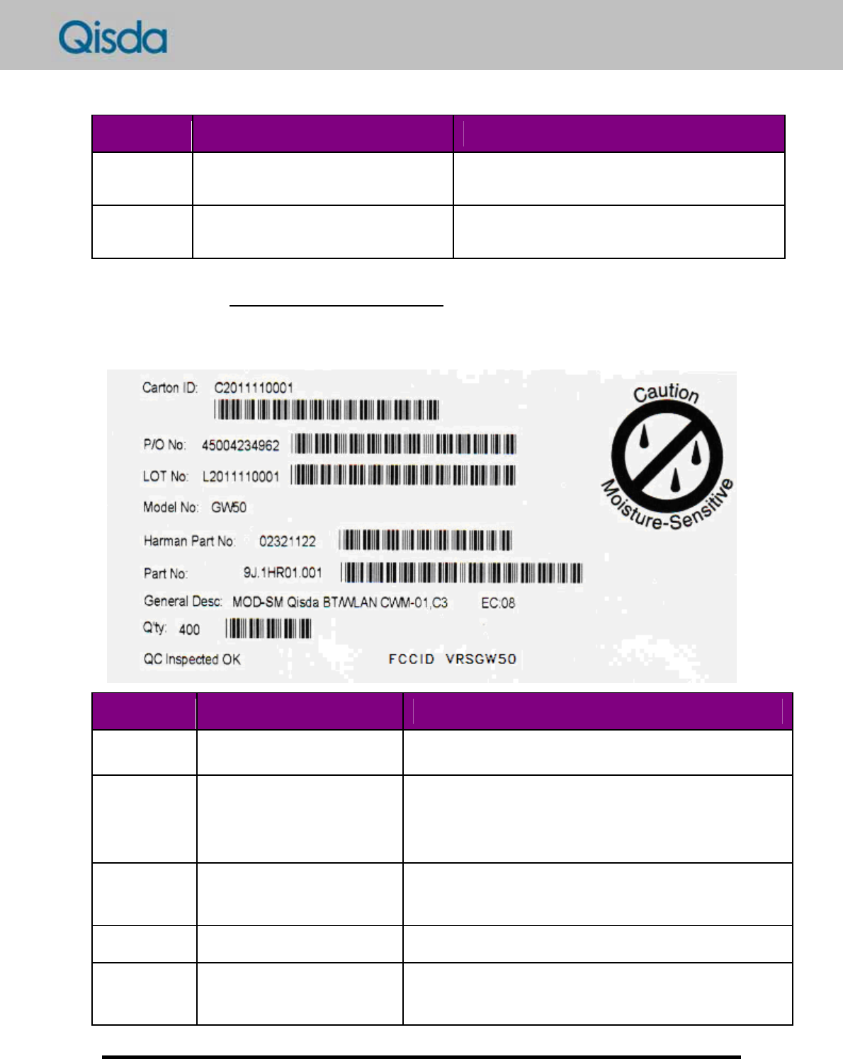
7.2.3.2. Carton Label: The L50*W15 mm dimensions’ Carton Label, printed on
Carton, is prepared for the W50 moving caution language. Please see
the below picture on the W50 Carton:
7.2.3.3. Caution Label: The L55*W55 mm dimensions’ Caution Label is pre-
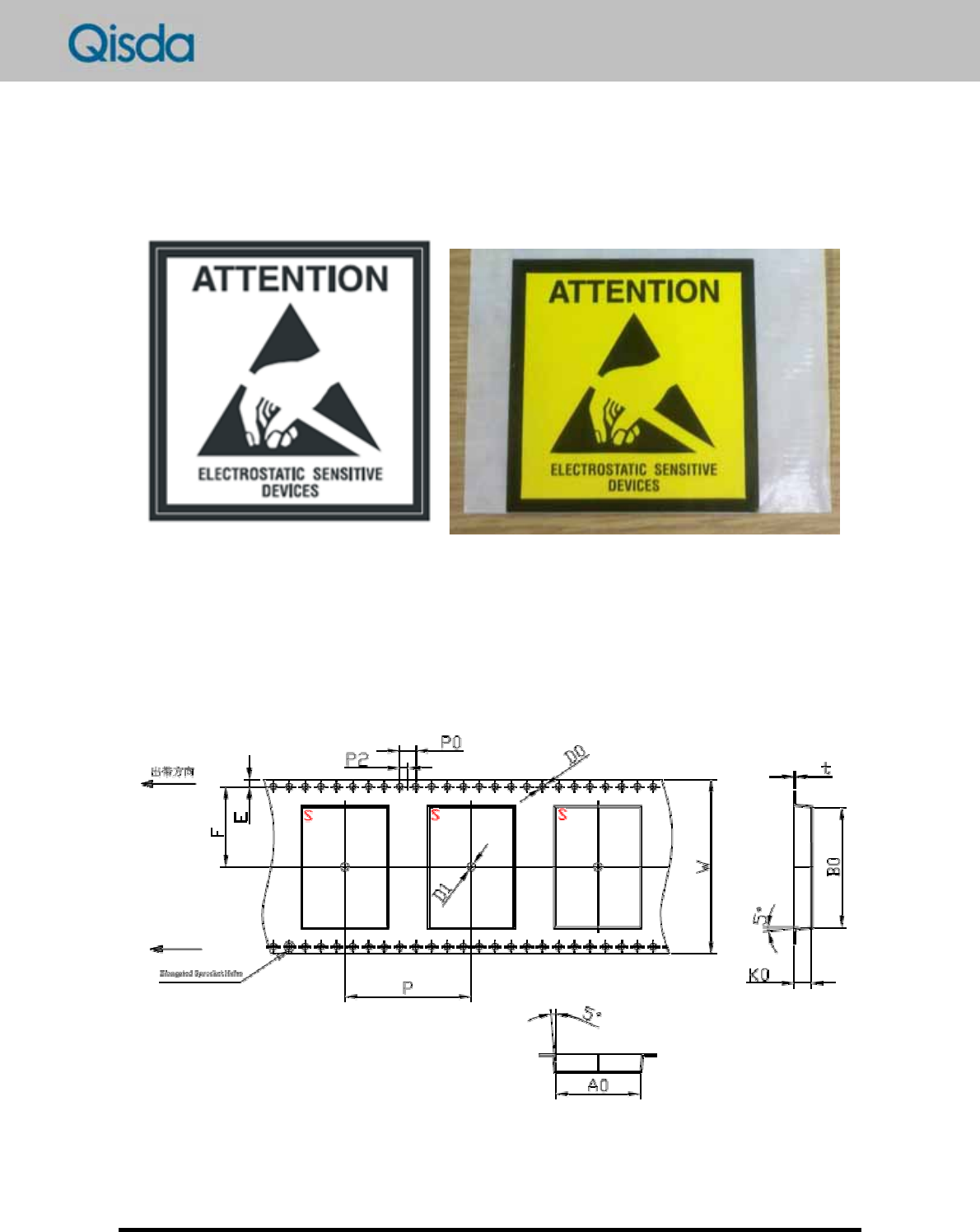
- 36 - Version: 0.0.1 – 2011/12/02
pared for the ESD Indicator purpose. The P/N has been defined as
4E.G3503.00. Please see the below illustration and picture for the W50
Caution Label:
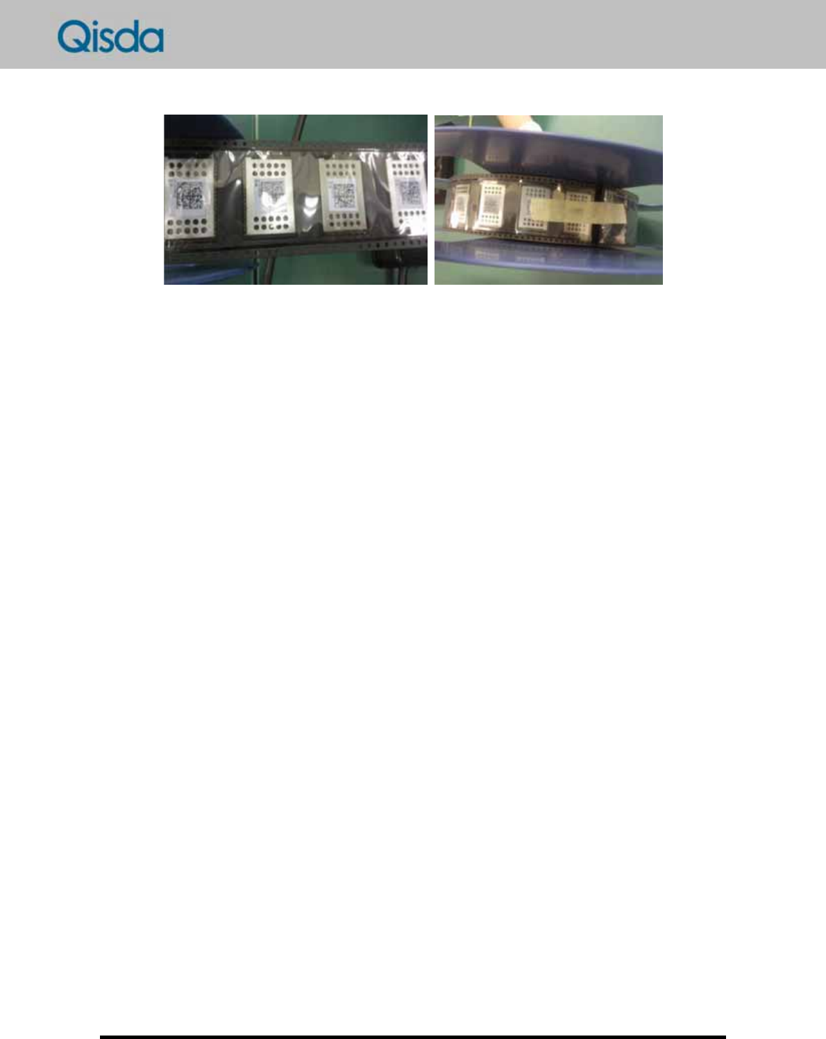
7.2.4. Tapes: The 400 pcs W50 of per Reel with PS Black Cover and Carrier
Tapes are prepared for the W50 Module packaging, met to ESD stan-
dard Ohm: 10^4Ω~10^6Ω and EIA-481-D. The P/N has been defined as
Cover Tap-4B.1HR01.001 and Carrier Tap-4B.1HR03.001. Please see the
below illustration and pictures for the W50 Carrier and Cover Tapes:
- 37 - Version: 0.0.1 – 2011/12/02
7.3. Shipment, storage and handling
The W50 Shipment, Storage and Handling are based and acting on per Carton
with 5 Pizza Box packages and 2,000 pcs W50 inside.
8. Certifications
8.1. FCC Regulations:
This device complies with part 15 of the FCC Rules. Operation is subject to the following
two conditions: (1) This device may not cause harmful interference, and (2) this device must
accept any interference received, including interference that may cause undesired operation.
This device has been tested and found to comply with the limits for a Class B digital de-
vice, pursuant to Part 15 of the FCC Rules. These limits are designed to provide reasonable
protection against harmful interference in a residential installation. This equipment generates,
uses and can radiated radio frequency energy and, if not installed and used in accordance with
the instructions, may cause harmful interference to radio communications. However, there is
no guarantee that interference will not occur in a particular installation If this equipment does
cause harmful interference to radio or television reception, which can be determined by turn-
ing the equipment off and on, the user is encouraged to try to correct the interference by one
or more of the following measures:
-Reorient or relocate the receiving antenna.
-Increase the separation between the equipment and receiver.
-Connect the equipment into an outlet on a circuit different from that to which the receiver is
connected.
-Consult the dealer or an experienced radio/TV technician for help.

- 38 - Version: 0.0.1 – 2011/12/02
Changes or modifications not expressly approved by the party responsible for compliance
could void the user‘s authority to operate the equipment.
RF Exposure Information
This Modular Approval is limited to OEM installation for mobile and fixed applications
only. The antenna installation and operating configurations of this transmitter, including any
applicable source-based time-averaging duty factor, antenna gain and cable loss must satisfy
MPE categorical Exclusion Requirements of §2.1091.
The antenna(s) used for this transmitter must be installed to provide a separation distance of
at least 20 cm from all persons, must not be collocated or operating in conjunction with any
other antenna or transmitter, except in accordance with FCC multi-transmitter product pro-
cedures.
The end user has no manual instructions to remove or install the device and a separate ap-
proval is required for all other operating configurations, including portable configurations
with respect to 2.1093 and different antenna configurations.
Maximum antenna gain allowed for use with this device is 2 dBi.
When the module is installed in the host device, the FCC ID label must be visible through a
window on the final device or it must be visible when an access panel, door or cover is easily
re-moved. If not, a second label must be placed on the outside of the final device that con-
tains the following text: “Contains FCC ID: VRSGW50”.
9. Contact
Qisda Corporation
18 Jihu Road, Neihu,
Taipei 114, Taiwan
Tel: +886 2 2799-8800
Fax: +886 2 2799-9688
Website: Qisda.com