Qisda GW52 MOD-SM QIS BT/WLAN CWM-02B-BT2-SP D5 User Manual
Qisda Corporation MOD-SM QIS BT/WLAN CWM-02B-BT2-SP D5
Qisda >
User Manual

Product System (PS)
Form No: QTY0-0B-008-05(120104)
1
GW52 Datasheet
Product System (PS)
Form No: QTY0-0B-008-05(120104)
2
Revision History
Version
History
Date
Author
1
Initial Version
2016/01/06
Kuo Fang
2
Add Electrical Characteristics
Add Reset timing and Power on /off
sequence
2016/01/20
Kuo Fang
3
Modify :
a. Block Diagram
b. Wording
c. Module PCB Pad & Stencil design
recommendation
d. Reflow Profile
Technical change:
a. Change BT output power: -3.3dBm to
-2.5dBm
Add part:
a. Bluetooth power class : Class 2
b. Module Label Content
c. Packing Drawing
d. Packing Label Drawing
e. Floor Life and Shelf Life (IPC
J-STD-033B)
2016/01/26
Kuo Fang
4
Add 1.1 Ordering Information
Modify : Wording
2016/03/08
Joseph Lin

Product System (PS)
Form No: QTY0-0B-008-05(120104)
3
Table of Contents
1. INTRODUCTION ................................................................................................................................... 5
1.1 Ordering Information ......................................................................................................... 5
2. REFERENCE DOCUMENT ................................................................................................................... 5
3. REQUIREMENT ................................................................................................................................... 6
3.1 H/W Requirement................................................................................................................ 6
3.1.3 Host Interface - SDIO Interface ............................................................................ 8
3.1.4 UART Interface ......................................................................................................... 8
3.1.5 WLAN_RF .................................................................................................................. 8
3.1.6 BT_RF ......................................................................................................................... 8
3.1.7 Digital Audio Interface ........................................................................................... 9
3.1.8 Sleep_CLK ................................................................................................................ 9
3.1.9 Joint Test Action Group (JTAG) and Test Interface ...................................... 9
3.1.10 Antenna Diagnosis ............................................................................................... 9
3.1.11 Antenna Select .................................................................................................... 10
3.1.12 VCC_VIO ................................................................................................................ 11
3.1.13 VCC_3V3 ............................................................................................................... 11
3.1.14 RF Subsystem Requirement ............................................................................ 11
3.1.14.1 Radio Specification 802.11B/G WLAN ............................................... 11
3.1.14.2 Radio Specification 802.15 Bluetooth ................................................ 12
3.1.15 BB Subsystem Requirement ........................................................................... 13
3.1.15.1 PIN Assignment ....................................................................................... 13
3.1.16 Critical Component Lists .................................................................................. 14
3.1.17 Reset Timing and Power on /off Sequence ................................................. 14
3.2 Electrical Characteristics ............................................................................................... 16
3.3 S/W Requirement .............................................................................................................. 17
3.4 Mechanical Requirement ................................................................................................ 17
3.4.1 Form factor ............................................................................................................. 17
3.4.2 Dimension ............................................................................................................... 17
3.4.3 Weight ...................................................................................................................... 17
3.4.4 Drawing .................................................................................................................... 18
3.4.5 PCB Pad & Stencil Design Recommendation ............................................... 19
4. MAINTAINABILITY & QUALITY ......................................................................................................... 20
4.1 Maintainability ................................................................................................................... 20
4.2 Quality Target .................................................................................................................... 20
5. ENVIRONMENTAL REQUIREMENTS .................................................................................................. 20
5.1 Operating and Storage Requirements ........................................................................ 20

Product System (PS)
Form No: QTY0-0B-008-05(120104)
4
5.1.1 Temperature ........................................................................................................... 20
5.1.2 Floor Life ................................................................................................................. 20
5.1.3 Shelf Life.................................................................................................................. 20
6. HANDLING REQUIREMENTS............................................................................................................. 20
7. REFLOW PROFILE ............................................................................................................................ 21
8. MODULE LABEL CONTENT ............................................................................................................. 22
9. PACKING DRAWING ......................................................................................................................... 23
10. PACKING LABEL DRAWING .......................................................................................................... 24
11. CERTIFICATIONS ............................................................................................................................ 25
11.1. FCC Regulations: .......................................................................................................... 25
12. CONTACT ....................................................................................................................................... 26
Product System (PS)
Form No: QTY0-0B-008-05(120104)
5
1. INTRODUCTION
GW52 is built on the Marvell® 88W8787 low-cost highly-integrated IEEE
802.11b/g/n MAC/Baseband/RF WLAN and Bluetooth Baseband/RF system-on-chip
(SoC).The module supports IEEE 802.11n with maximum data rates up to 72Mbps
(20 MHz channel) and 150 Mbps (40MHz), 802.11g payload data rates of 6, 9, 12, 18,
24, 36, 48, and 54 Mbps, as well as 802.11b data rates of 1, 2, 5.5 and 11 Mbps for
WLAN operation.
For Bluetooth operation, the module supports Bluetooth 3.0 + High Speed (HS)
(also compliant with Bluetooth 2.1 + EDR).
For security, the 88W8787 supports the IEEE 802.11i security standard through
implementation of the Advanced Encryption Standard (AES)/Counter Mode
CBC-MAC Protocol (CCMP), and Wired Equivalent Privacy (WEP) with Temporal Key
Integrity Protocol (TKIP) security mechanisms.
The module also supports Internet Protocol Security (IPsec) with DES/3DES/AES
encryption and MD5/SHA-1 authentication as well as 802.11e Quality of Service
(QoS). The module supports dual SDIO host interface for connecting the WLAN and
Bluetooth to the host processor. For Bluetooth application the high-speed UART (up
to 4MB/s, PCM/Inter-IC Sound (I2S), are supported too.
For better throughput of WLAN/BT the module provide different RF paths for WLAN
and Bluetooth for two antennas. By using of two antennas with enough decoupling it
enables to do without coexistence.
1.1 Ordering Information
Harman P/N
Qisda P/N
Descriptions
02932261
9J.35R02.001
D5 variant, Dual Antenna 802.11b/g/n + Bluetooth
3.0 Module
2. REFERENCE DOCUMENT
IEEE Std 802.11b-1999 (Supplement to ANSI/IEEE Std 802.11, 1999 Edition)
IEEE Std 802.11g.-2003 (Amendment to IEEE Std 802.11, 1999 Edition)
IEEE Std 802.11n -2009 (Amendment 5: Enhancements for Higher Throughput)
SIG Std Master Table of Contents & Compliance Requirements
Product System (PS)
Form No: QTY0-0B-008-05(120104)
6
3. REQUIREMENT
3.1 H/W Requirement
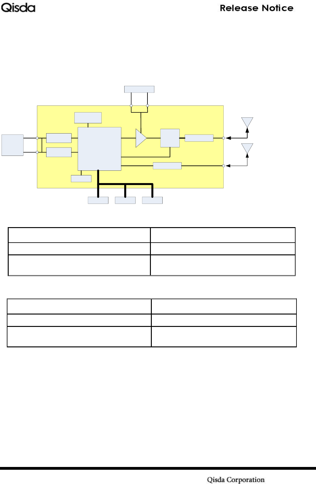
3.1.1 H/W Block Diagram
88W8787
WLAN/BT
PA
Band pass filter
EEPROM
Crystal
SP2T
Switch Band pass filter
UART SDIO PCM
LDO
3.3V to 3V
VCC_3.3V
LDO
3.3V to 1.8V
VCC_3V3
Module
Pin 23
Pin 24
Pin 32
Pin 33
WLAN
Antenna
BT
Antenna
AS179-92LF
LX5511LQ-TR
EXS00A-CS05684
MAX4835ETT18BD2V+T
TLV70030QDCKRQ1
DEA162450BT-1260B2
DEA162450BT-1260B2
25AA080CT-I/MS
88W8787-A1-BRD2A000-P123
WLAN TX
WLAN RX
BT TX/RX
Pin 17
Pin 2
Crystal Frequency: 38.4 MHz
WLAN frequency:
Features
Description
Frequency Band
2.401 – 2.473GHz
Number of selectable Sub channels
11channels
(f=2412+n*5MHz,n=1,…,11)
Channel 12 and 13 of WiFi 2.4G band are permanently disabled
Bluetooth frequency:
Features
Description
Frequency Band
2.401 – 2.480GHz
Number of selectable Sub
channels
79 channels
(f=2402+k MHz, k=0,…,78)
3.1.2 System Interface
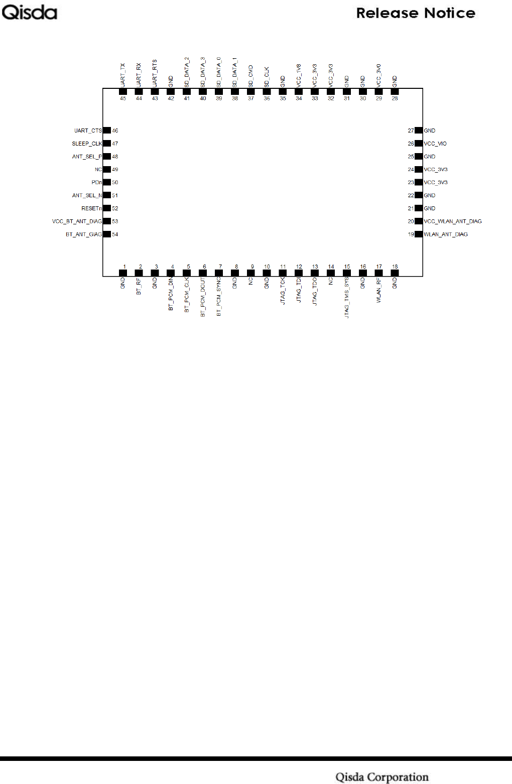
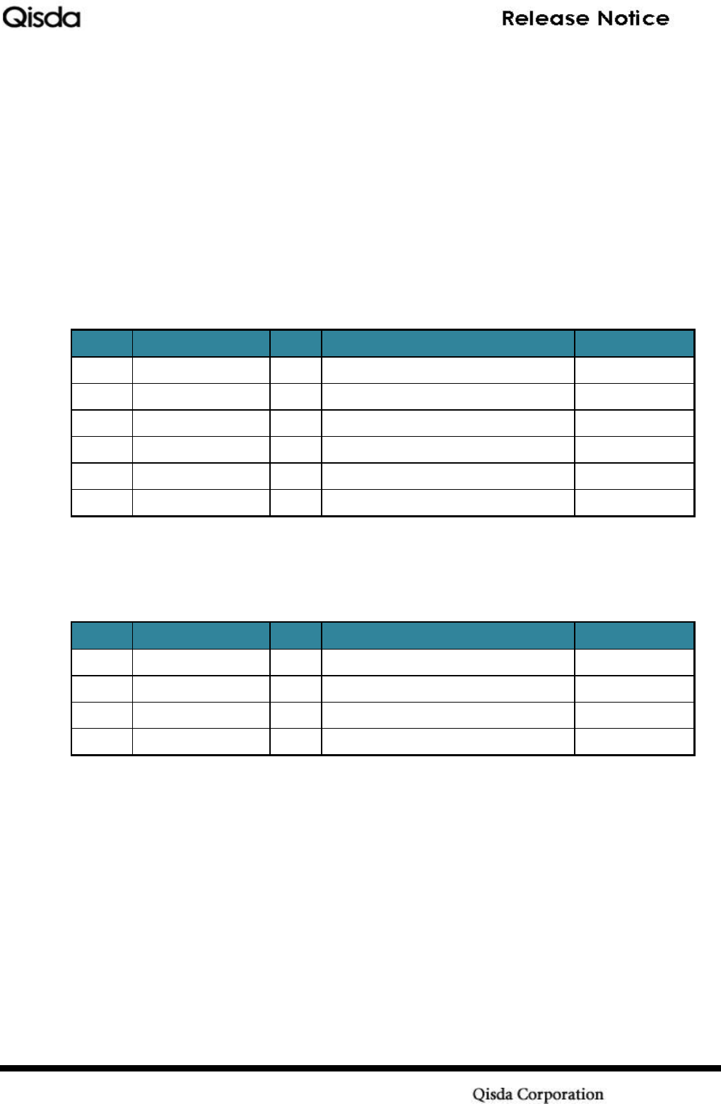
The form factor of GW52 module is 54 pins stamp hole.
The pin define of GW52 is shown in Figure 3-1 System Interface.
Product System (PS)
Form No: QTY0-0B-008-05(120104)
7
Figure 3-1 System Interface
Product System (PS)
Form No: QTY0-0B-008-05(120104)
8
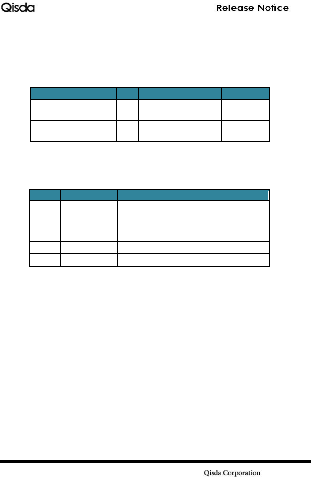
3.1.3 Host Interface - SDIO Interface
The GW52 with SDIO interface which comply with the high speed mode of SDIO
1.2 specification. The host controller could use the SDIO bus to access data from
the WLAN and/or Bluetooth device. There are two independent client drivers for
WLAN and/or Bluetooth inside the host software. Due to both of WLAN and BT
device share the same SDIO interface, the SDIO bus driver inside host software
contain an arbitration scheme.
The SDIO interface supports 4-bit SDIO transfer modes at the full clock range
of 0 to 50MHz.
Pin #
Signal Name
I/O
Signal Description
Supply
36
SD_CLK
I
SDIO clock
VCC_VIO
37
SD_CMD
I/O
SDIO command line
VCC_VIO
39
SD_DAT_0
I/O
SDIO data line bit 0
VCC_VIO
38
SD_DAT_1
I/O
SDIO data line bit 1
VCC_VIO
41
SD_DAT_2
I/O
SDIO data line bit 2
VCC_VIO
40
SD_DAT_3
I/O
SDIO data line bit 3
VCC_VIO
3.1.4 UART Interface
The GW52 module supports a high speed UART interface, compliant to the
industry standard 16550 specification. (For debug only)
Pin #
Signal Name
I/O
Signal Description
Supply
45
UART_TX
O
UART serial data output
VCC_VIO
44
UART_RX
I
UART serial data input
VCC_VIO
46
UART_CTS
I
UART Clear to send signal
VCC_VIO
43
UART_RTS
O
UART Ready to send signal
VCC_VIO
3.1.5 WLAN_RF
WLAN antenna input/output. The pin is connected to WLAN antenna. The
impedance of trace or antenna should be designed to 50 ohm.
3.1.6 BT_RF
Bluetooth antenna input/output. The pin is connected to BT antenna. The
impedance of trace or antenna should be designed to 50 ohm.
Product System (PS)
Form No: QTY0-0B-008-05(120104)
9
3.1.7 Digital Audio Interface
PCM interface supports continual transmission and reception of PCM data
without processor overhead. The PCM support data rates from 64 KHz to
2.048MHz with multi-slot handshake and synchronization PCM encoding/decoding
with A-law, μ-law, and linear voice.
Pin #
Signal Name
I/O
Signal Description
Supply
5
BT_PCM_CLK
I/O
PCM clock
VCC_VIO
7
BT_PCM_SYNC
I/O
PCM sync pulse
VCC_VIO
4
BT_PCM_DIN
I
PCM data input
VCC_VIO
6
BT_PCM_DOUT
O
PCM data output
VCC_VIO
3.1.8 Sleep_CLK
The sleep clock can be providing from external clock source.
External Sleep Clock Timing:
Symbol
Parameter
Min.
Typ.
Max
Units
CLK
Clock Frequency
32 or 32.768
-50ppm
32 or
32.768
32 or 32.768
+50ppm
KHz
THIGH
Clock high time
40
ns
TLOW
Clock low time
40
ns
TRISE
Clock rising time
5
ns
TFALL
Clock falling time
5
ns
3.1.9 Joint Test Action Group (JTAG) and Test Interface
JTAG is reserved for SW debug and failure analysis.
3.1.10 Antenna Diagnosis
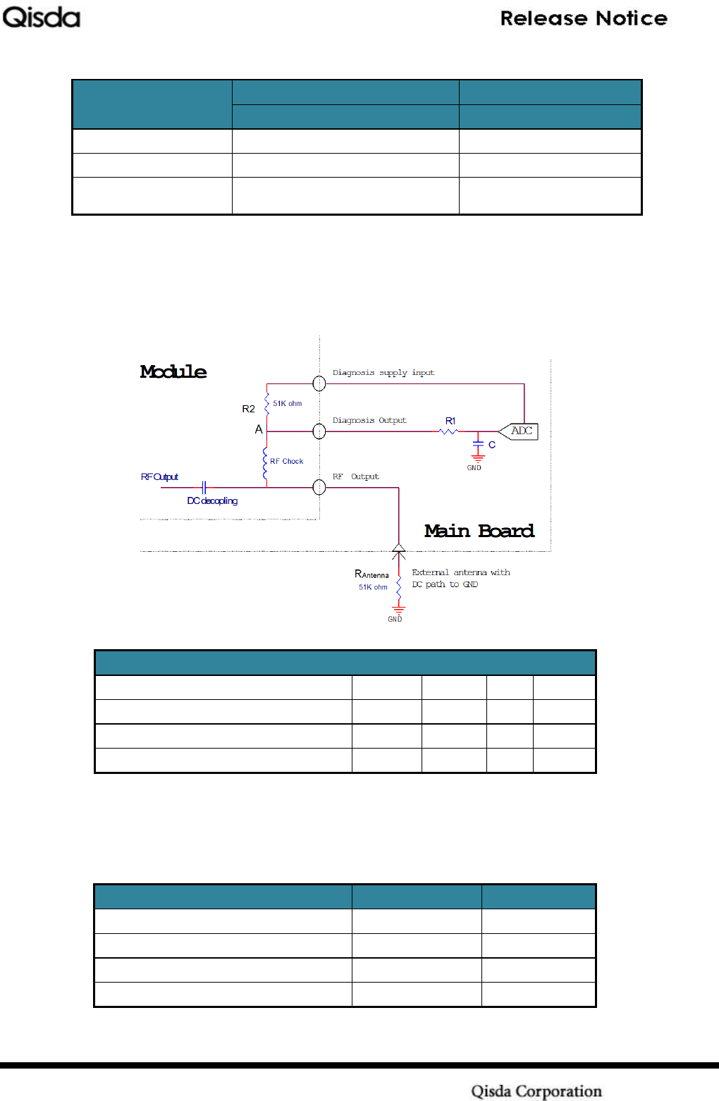
Antenna Diagnosis circuit is used to detect the connection status between
external antenna and GW52 RF ports. The reference schematics for antenna
diagnosis circuit are shown in Figure 3-2. The RAntenna is embedded in the external
antenna and cross between signal line and ground. RAntenna and R2 act as a voltage
divider.
There are three kinds of antenna connection status can be detected:
- Antenna port is open
- Antenna port is connected correctly
- Antenna port is short-circuited to GND.
The relationship between supply voltage of antenna diagnosis circuit and
measured voltage at point A are listed in Table 3-1.
Product System (PS)
Form No: QTY0-0B-008-05(120104)
10
Antenna
connection status
VCC_WLAN_ANT_DIAG=V1
WLAN_ANT_DIAG=V2
VCC_BT_ANT_DIAG
BT_ANT_DIAG
connected correctly
V1/2
V2/2
Open
V1
V2
Short-circuited to
Ground
0 V
0V
Table 3-1
R1 and C act as a low pass filter for removing all frequencies above the Nyquist
frequency. The resistor R1 can limit the current flowing into ADC if antenna
connector is short-circuited to battery voltage. The recommended value for RAntenna ,
R1 and C are listed in Table 3-2 Antenna interface.
Figure 3-2 Antenna interface
Antenna Diagnosis
Min
Typ
Max
Unit
RAntenna
51
K ohm
Proposal low pass filter R1
51
K ohm
Proposal low pass filter C
220
nF
Table 3-2 Recommendation for R1 & C
3.1.11 Antenna Select
ANT_SEL_P & ANT_SELN are differential control signals.
ANT_SEL_N
ANT_SEL_P
Antenna
0
0
0 (default)
1 (default)
Antenna 1
1
0
Antenna 0
1
1
Product System (PS)
Form No: QTY0-0B-008-05(120104)
11
3.1.12 VCC_VIO
VCC_VIO is an external power supply for interface. (3.3V or 1.8V)
VIO pin should be connected to the same supply.
3.1.13 VCC_3V3
The module draws all its power from the 3.3V supply.
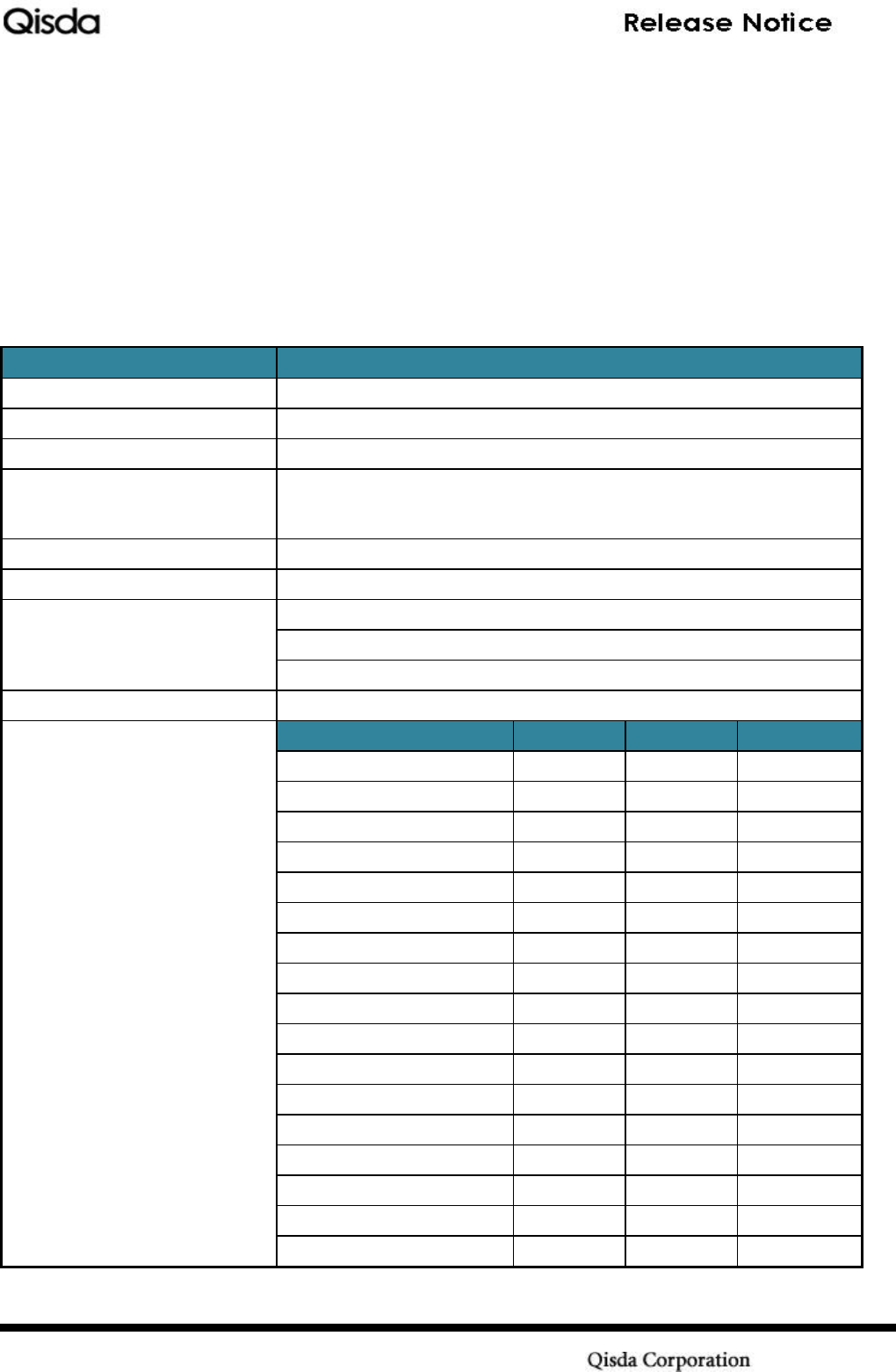
3.1.14 RF Subsystem Requirement
3.1.14.1 Radio Specification 802.11B/G WLAN
Features
Description
Frequency Band
2.4000 – 2.4835 GHz (2.4 GHz ISM Band)
Number of selectable Sub
11 channels
Channels
(f=2412+n*5MHz,n=0,…,12)
Modulation
OFDM,DSSS (Direct Sequence Spread Spectrum), DBPSK,DQPSK,
CCK ,16QAM, 64QAM
Supported rates
1, 2, 5.5, 11, 6, 9, 12, 18, 24, 36, 48, 54 Mbps
Maximum receive level
-10dBm (with PER < 8%)
Output Power
b Mode : 15±1.5 dBm @ 1, 2, 5.5, and 11Mbps
g Mode : 15±1.5 dBm @ 6, 9, 12, 18, 24, 36, 48 and 54Mbps
n mode : 15±1.5 dBm @ MCS0~7 HT20 & HT40
Carrier Frequency Accuracy
-2ppm~+2ppm in 25℃
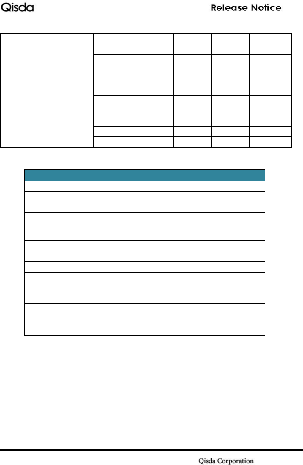
Sensitivity
Data Rate
Minimum
Typical
Maximum
802.11b @ 1Mbps
-94dBm
802.11b @ 2Mbps
-91dBm
802.11b @ 5.5Mbps
-89dBm
802.11b @ 11Mbps
-86dBm
802.11g @ 6Mbps
-88dBm
802.11g @ 9Mbps
-87dBm
802.11g @ 12Mbps
-85dBm
802.11g @ 18Mbps
-84dBm
802.11g @ 24Mbps
-80dBm
802.11g @ 36Mbps
-77dBm
802.11g @ 48Mbps
-73dBm
802.11g @ 54Mbps
-72dBm
802.11n @HT20 MCS0
-82dBm
802.11n @HT20 MCS1
-79dBm
802.11n @HT20 MCS2
-77dBm
802.11n @HT20 MCS3
-74dBm
802.11n @HT20 MCS4
-70dBm
Product System (PS)
Form No: QTY0-0B-008-05(120104)
12
802.11n @HT20 MCS5
-66dBm
802.11n @HT20 MCS6
-65dBm
802.11n @HT20 MCS7
-64dBm
802.11n @HT40 MCS0
-79dBm
802.11n @HT40 MCS1
-76dBm
802.11n @HT40 MCS2
-74dBm
802.11n @HT40 MCS3
-71dBm
802.11n @HT40 MCS4
-67dBm
802.11n @HT40 MCS5
-63dBm
802.11n @HT40 MCS6
-62dBm
802.11n @HT40 MCS7
-61dBm
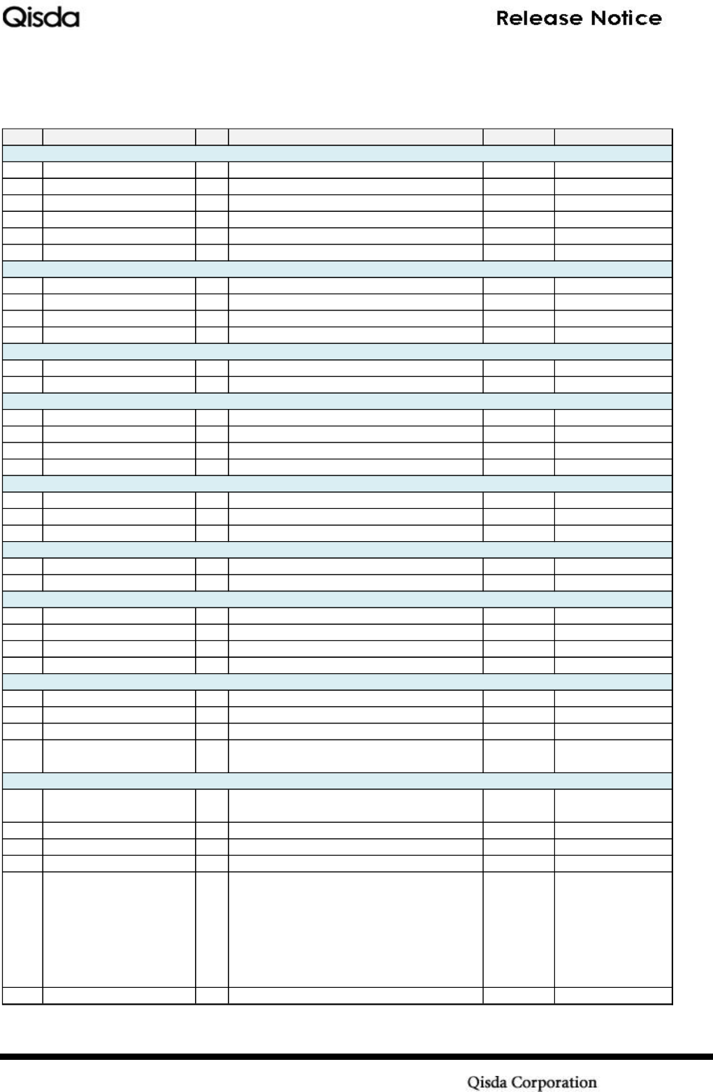
3.1.14.2 Radio Specification 802.15 Bluetooth
Features
Description
Frequency Band
2.4 GHz ISM Band
Number of selectable Sub
79 channels
Channels
(f=2402+k MHz, k=0,…,78)
Modulation
FHSS (Frequency Hopping Spread
Spectrum)
GFSK, π/4-DQPSK, 8DPSK
Supported rates
1, 2, 3 Mbps
Maximum receive level
-10dBm (with PER < 8%)
Power Class
Class 2
Output Power
Channel 2402 :-2.5dBm~1dBm
Channel 2441 :-2.5dBm~1dBm
Channel 2479: -2.5dBm~1dBm
Sensitivity
1Mbps: -80dBm @ 0.1% BER
2Mbps: -77dBm @ 0.01% BER
3Mbps: -80dBm @ 0.01% BER
Product System (PS)
Form No: QTY0-0B-008-05(120104)
13
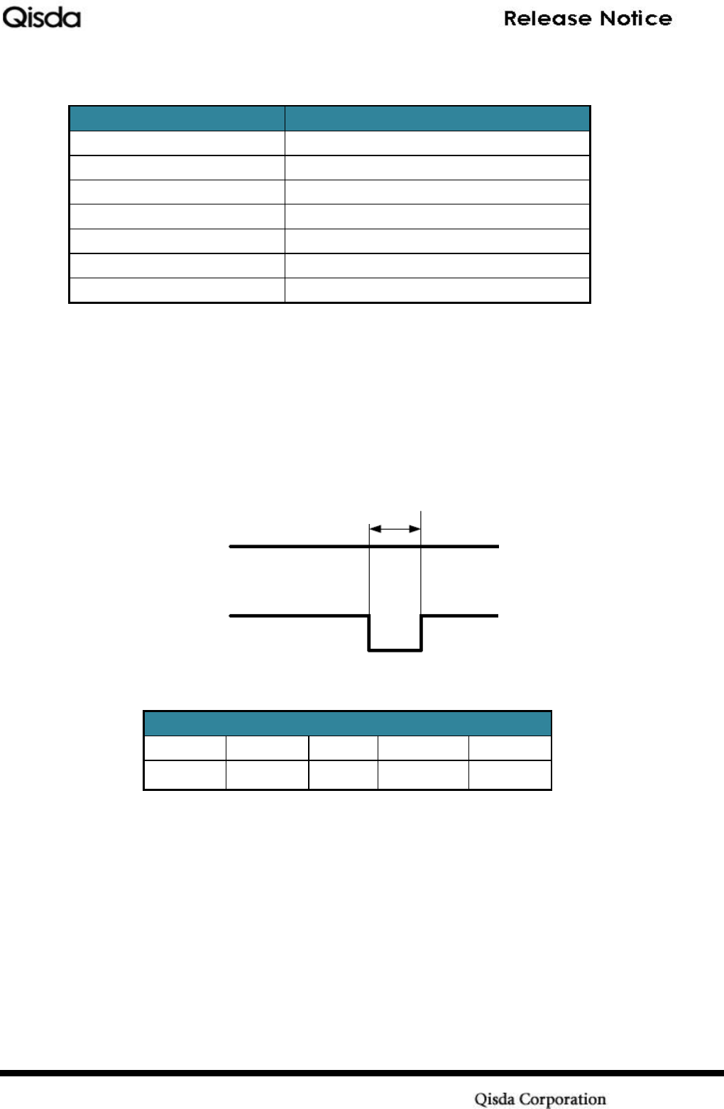
3.1.15 BB Subsystem Requirement
3.1.15.1 PIN Assignment
Pin # Sig nal Name I/O Signal Description Supply Remark
36 SD_CLK I SDIO clock VCC_VIO
37 SD_CMD I/O SDIO command line VCC_VIO
39 SD_DAT_0 I/O SDIO data line bit 0 VCC_VIO
38 SD_DAT_1 I/O SDIO data line bit 1 VCC_VIO
41 SD_DAT_2 I/O SDIO data line bit 2 VCC_VIO
40 SD_DAT_3 I/O SDIO data line bit 3 VCC_VIO
45 UART_TX O UART serial data output VCC_VIO
44 UART_RX I UART serial data input VCC_VIO
46 UART_CTS I UART Clear to send signal VCC_VIO
43 UART_RTS O UART Ready to send signal VCC_VIO
17 WLAN_RF I/O WLAN antenna in/out
2 BT_RF I/O Bluetooth antenna in/out
5 BT_PCM_CLK I/O PCM clock VCC_VIO
7 BT_PCM_SYNC I/O PCM sync pulse VCC_VIO
4 BT_PCM_DIN I PCM data input VCC_VIO
6 BT_PCM_DOUT O PCM data output VCC_VIO
52 RESETn I Reset signal VCC_VIO Active low
47 SLEEP_CLK I Sleep clock VCC_VIO
50 PDn I Full power down VCC_VIO Active low
48 ANT_SEL_P O Differential Antenna Select Positive output VCC_3V0
51 ANT_SEL_N O Differential Antenna Select Negative output VCC_3V0
53 VCC_BT_ANT_DIAG I External power for BT antenna diagnosis
54 BT_ANT_DIAG O BT antenna diagnosis output
20 VCC_WLAN_ANT_DIAG I External power for WLAN antenna diagnosis
19 WLAN_ANT_DIAG O WLAN antenna diagnosis output
11 JTAG_TCK I JTAG Tset Clock VCC_VIO
12 JTAG_TDI I JTAG Tset Data Input VCC_VIO
13 JTAG_TDO O JTAG Test Data Output VCC_VIO
15 JTAG_TMS_SYS I
JTAG Test Mode Select
(Selects theSystem JTAG controller)
VCC_VIO
23,24,
32,33
VCC_3V3 PI 3.3V power input
29 VCC_3V0 PO 3.0V monitoring output Leave unconnected.
34 VCC_1V8 PO 1.8V monitoring output Leave unconnected.
9,26 VCC_VIO PI 1.8/3.3V Host Interface Supply
14, 49 NC Not connected Leave unconnected.
Antenna Diagnosis
Joint Test Action Group (JTAG) and Test Interface
1,3,8,
10,16,
18,21,
22,25,
27,28,
30,31,
35,42,
GND
Power & Gro und
P
Ground
Antenna Select
SDIO Interface
Control & Power Interface
UART Interface
WLAN and Bluetooth RF Interface
Audio Interface – PCM
Product System (PS)
Form No: QTY0-0B-008-05(120104)
14
3.1.16 Critical Component Lists
Components
Product Name
BT/WIFI PROCESSOR SOC
Marvell -88W8787-A1-BRD2A000-P123
LDO REGULATOR IC
MAXIM - MAX4835ETT18BD2+T
POWER AMPLIFIER
MICROSEMI - LX5511LQ-TR
ANALOG SWITCH
SKYWORKS - AS179-92LF
EEPROM
MICROCHIP – 25AA080CT-I/MS
BANDPASS FILTER
TDK - DEA162450BT-1260B2
QUARTZ CRYSTAL
NDK - EXS00A-CS05684
3.1.17 Reset Timing and Power on /off Sequence
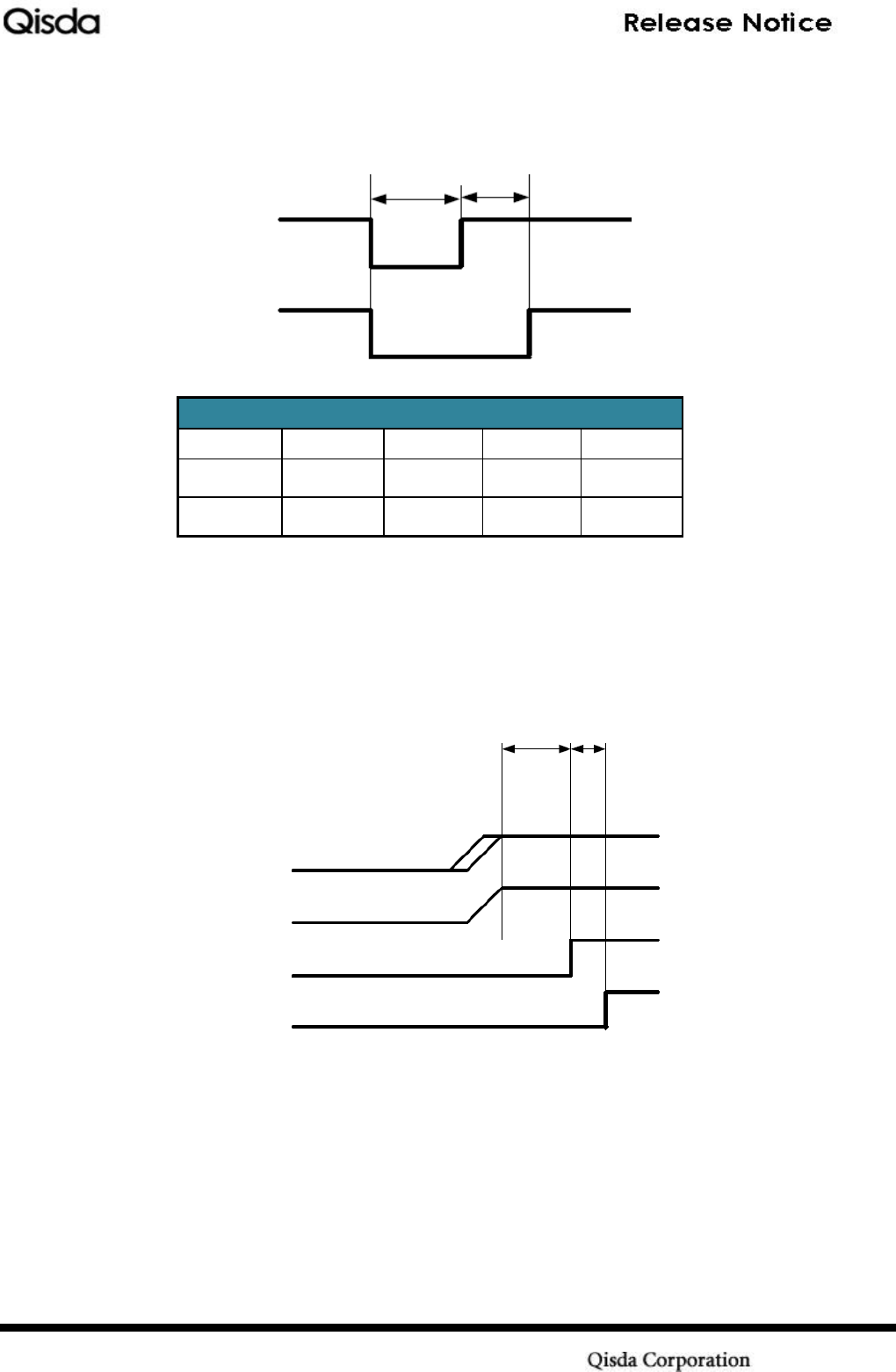
RESETn & PDn
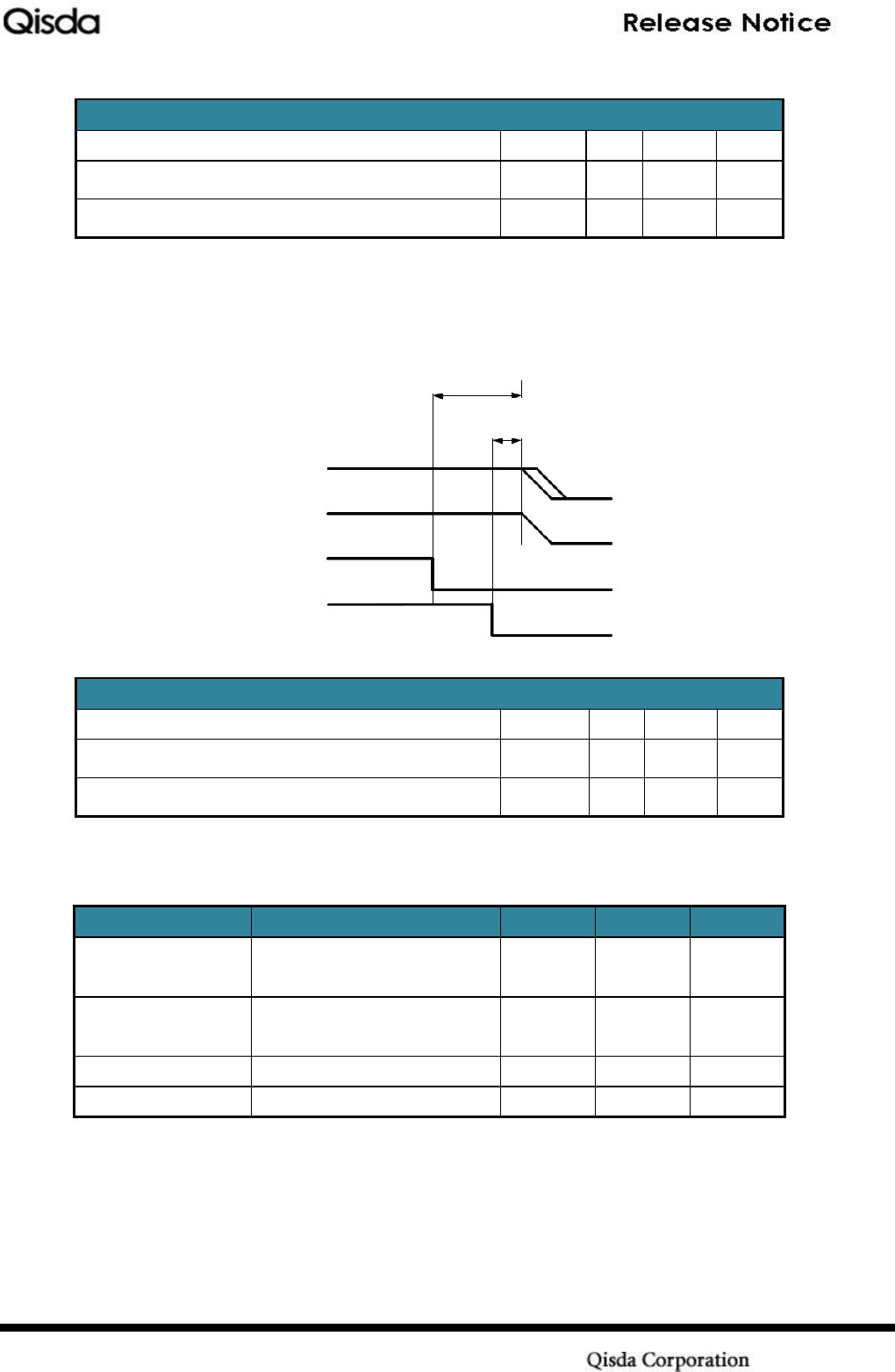
The module can be reset anytime by pulling down the RESETn for at least 5ms. It
is also possible to reset the module by PDn-RESETn sequence, the low duration
for PDn should be at least 700ms.
Reset by RESETn
RESET timing
min
typ
max
unit
tRST
5
ms
PDn
RESETn
H
H
L
L
tRST
Product System (PS)
Form No: QTY0-0B-008-05(120104)
15
Reset by RESETn & PDn
RESET timing
min
typ
max
unit
tPD
700
ms
tRST
5
ms
Power on sequence
When power on the module, the external powers and PDn and RESETn have to
meet the power sequence requirement, then the module can be powered on
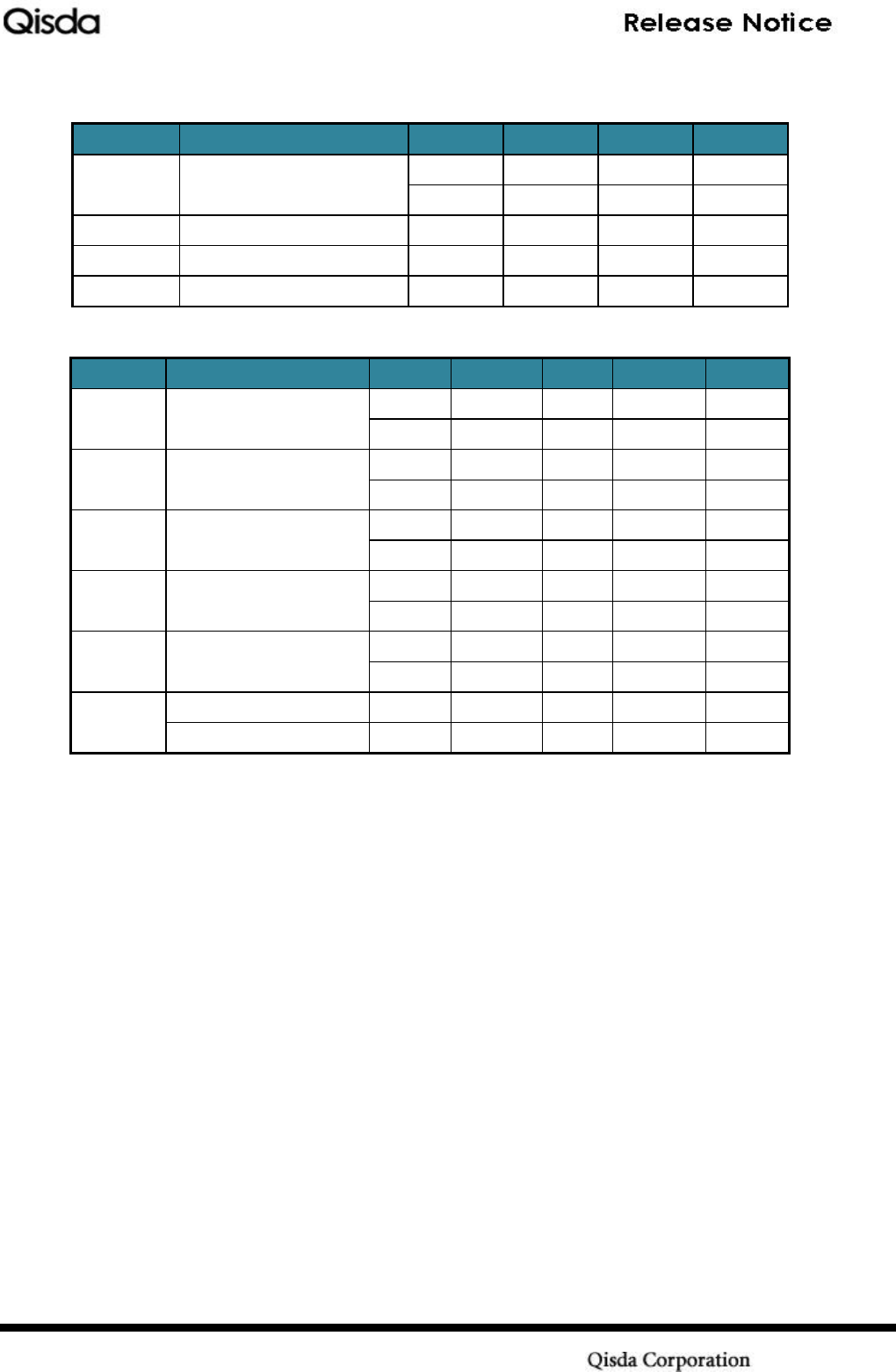
successfully and function well. The VCC_VIO can be rise before VCC_3V3 but the
rising of VCC_VIO should not be later than VCC_3V3.
EESETn
PDn
H
L
H
L
tRST
tPD
RESET
n
PD
n
H
L
H
L
tRST
tPD
PDn
RESETn
VCC_VIO
VCC_3V3
Product System (PS)
Form No: QTY0-0B-008-05(120104)
16
RESET timing
min
typ
max
unit
RESETn to VCC_3V3, tPD
700
ms
RESETn to PDn , tRST
5
ms
Power off sequence
In order to power off the module, PDn and RESETn have to meet the power off
sequence.
RESETn and PDn timing
min
typ
max
unit
PDn to VCC_3V3, tPD
0
ms
RESETn to VCC_3V3, tRST
500
us
3.2 Electrical Characteristics
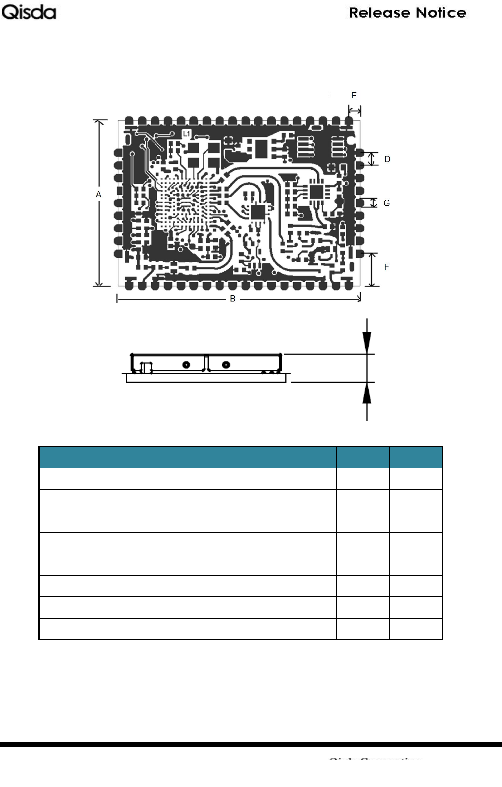
Absolute maximum ratings
Symbol
Parameter
Min.
Max.
Units
VCC_VIO
Power supply voltage
with respect to VSS
0
4.2
V
VCC_3V3
Power supply voltage
with respect to VSS
0
3.45
V
Tstg
Storage Temperature
-40
90
℃
Ta
Ambient Temperature
-40
90
℃
PDn
tRST
tPD
RESETn
VCC_VIO
VCC_3V3
Product System (PS)
Form No: QTY0-0B-008-05(120104)
17
Recommended operating conditions
Symbol
Parameter
Min.
Typ.
Max
Units
VCC_VIO
Digital I/O power supply
1.62
1.8
1.98
V
2.97
3.3
3.63
V
VCC_3V3
Main power supply
3.15
3.3
3.45
V
I_VIO
Current Supply VCC_VIO
205
mA
I_3V3
Current Supply 3V3
285
400
mA
DC Characteristics
Symbol
Parameters
Mode
Min.
Typ.
Max
Units
VIH
Input High Voltage
1.8V
1.2
2.1
V
3.3V
2.3
3.6
V
VIL
Input Low Voltage
1.8V
-0.3
0.6
V
3.3V
-0.3
1.1
V
VHYS
Input hysteresis
1.8V
250
mV
3.3V
400
mV
VOH
Output High Voltage
1.8V
1.22
V
3.3V
2.57
V
VOL
Output Low Voltage
1.8V
0.4
V
3.3V
0.4
V
PDn
PDn input, High level
1.4
5.5
V
PDn input, Low level
-0.3
0.5
V
3.3 S/W Requirement
MFG Test SW: MFG-8787-WIFI-SD-BT-SD-WIN-X86-1.2.7.23-14.0.11.p57
(Software of GW52 is design and will managed by customer)
3.4 Mechanical Requirement
3.4.1 Form factor
54 Pins LGA, 1.6mm Pitch
3.4.2 Dimension
21mm (L) x 30mm (W) x 4mm (H)
3.4.3 Weight
Typ: 3.67 (g)
Product System (PS)
Form No: QTY0-0B-008-05(120104)
18
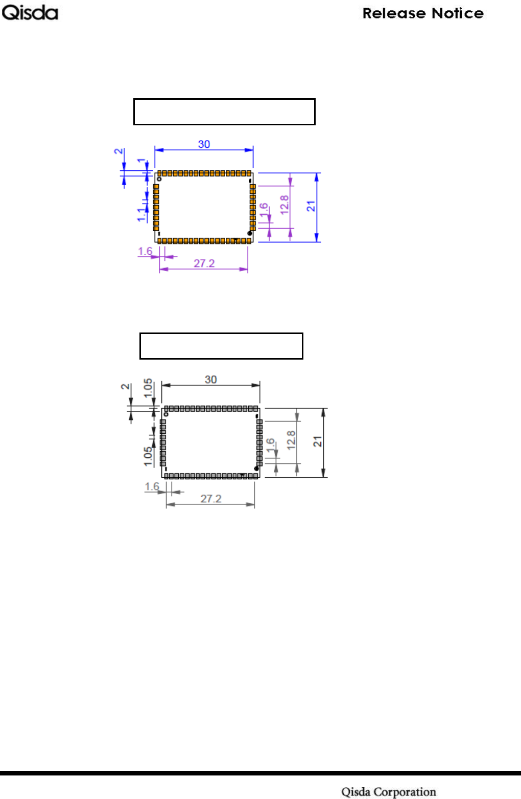
3.4.4 Drawing
Parameter
Description
Min.
Typ.
Max.
Units
A
Length
20.85
21
21.15
mm.
B
Width
29.85
30
30.15
mm.
C
Height
3.78
4
4.22
mm.
D
Pin To Pin Pitch
1.55
1.6
1.65
mm.
E
Edge To Pin Center
1.25
1.4
1.55
mm.
F
Edge To Pin Center
3.95
4.1
4.25
mm.
G
Pin Width
0.8
1
1.2
mm.
Weight
Weight
3.49
3.67
3.85
g
C
C
Product System (PS)
Form No: QTY0-0B-008-05(120104)
19
3.4.5 PCB Pad & Stencil Design Recommendation
WiFi + BT PCB PAD Design
WiFi + BT Stencil Design
Product System (PS)
Form No: QTY0-0B-008-05(120104)
20
4. MAINTAINABILITY & QUALITY
4.1 Maintainability
Module cannot be reworked.
Qisda will analyze failures and update report to customer by 8D format.
4.2 Quality Target
The quality target for the delivered quality (0 Km-line failures) is zero defects.
Quality target is complaint rate at delivery <50ppm.
5. ENVIRONMENTAL REQUIREMENTS
5.1 Operating and Storage Requirements
5.1.1 Temperature
Operating: - 40 to 90 °C
Storage: - 40 to 90 °C
5.1.2 Floor Life
Ambient Condition: ≦30 °C/60% RH
Maximum Floor time: 168 hour (MSL 3)
5.1.3 Shelf Life
When stored in a noncondensing atmospheric environment of < 40°C/90%
RH. (Moisture Barrier Bag)
6. HANDLING REQUIREMENTS
Do not touch any pin of module while assembling.
Product System (PS)
Form No: QTY0-0B-008-05(120104)
21
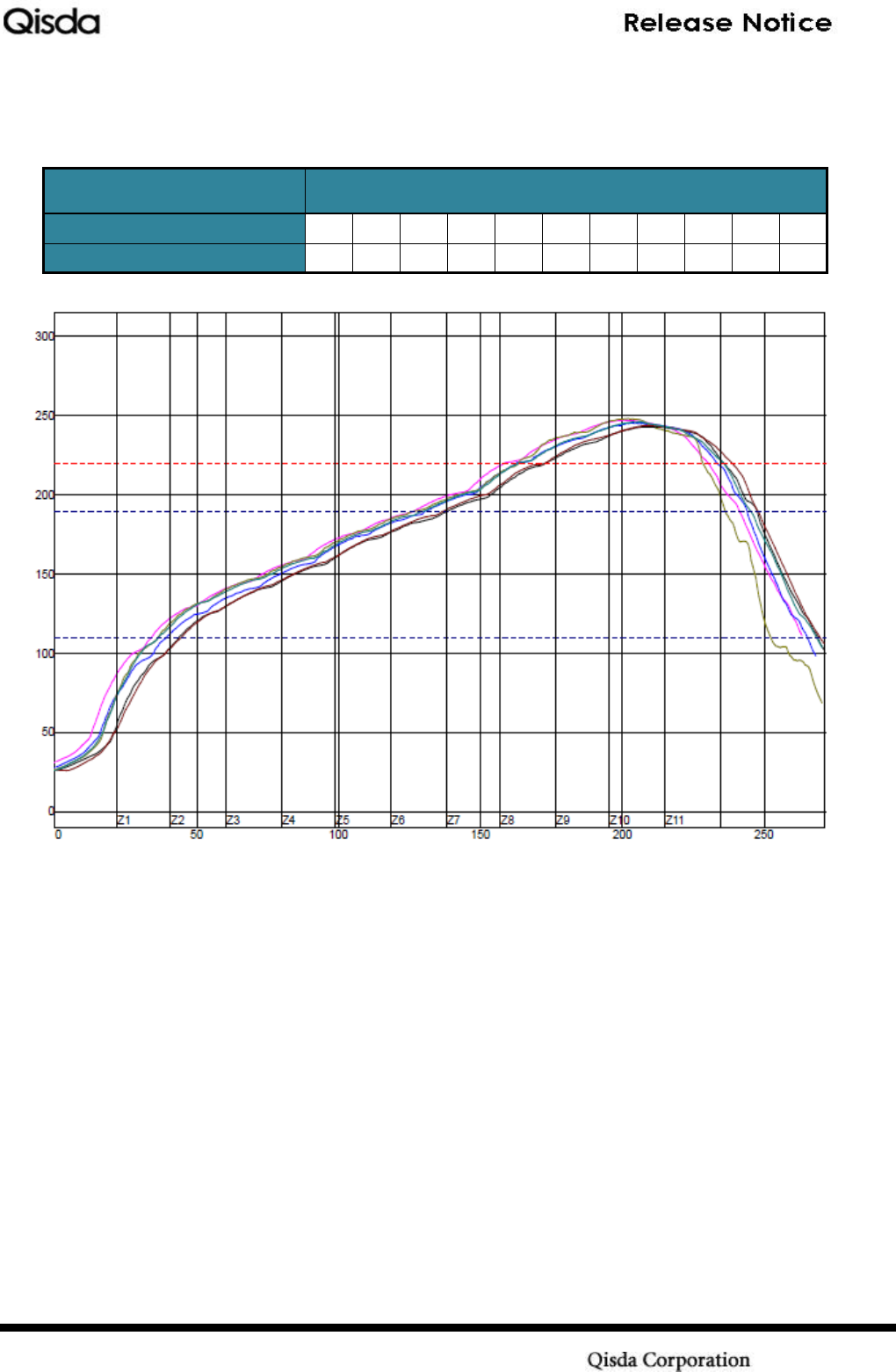
7. REFLOW PROFILE
Temperature setting (°C)
Conveyor speed : 110cm/1minute
Temperature region
Z1
Z2
Z3
Z4
Z5
Z6
Z7
Z8
Z9
Z10
Z11
The temperature zone
135
145
155
170
190
200
210
240
250
255
240
Product System (PS)
Form No: QTY0-0B-008-05(120104)
22
8. MODULE LABEL CONTENT
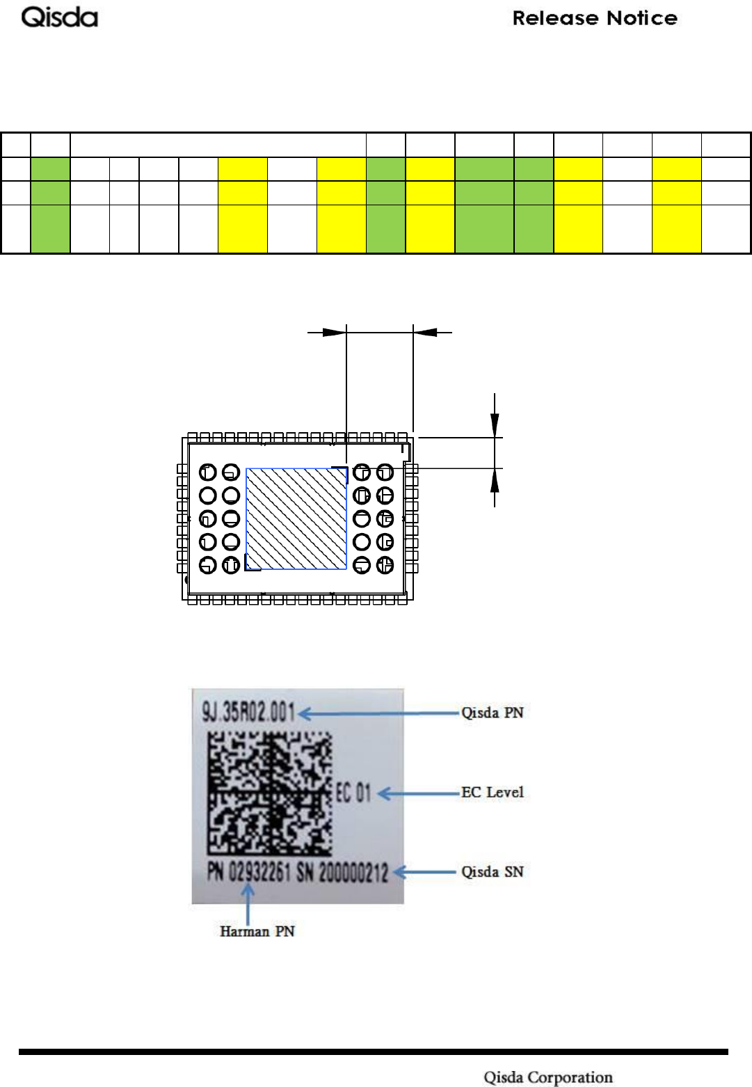
2D Barcode Definition
242
200000
001
01
01
029322
61,
LICHRG#
YYYYMM
DD,
PC#
GW52,
SN#
9J35R02001
A00,
MAC-AD
R#
XXXXXX
XXXXXX,
BLUE-TO
OTH#
XXXXXX
XXXXXX,
Digits
3
9
2
2
8+1
7
8+1
3
4+1
3
10
3+1
8
12+1
11
12+1
Desc.
Qisda
supplier
Code
Harman
Serial
No.
EC
Level
Harman
Module
No.
Harman
PCBA
Part.
No.
Fixed
Specified
Key
Supplier
Productio
n Date,
Fixed
Specified
Key
Qisda
Internal
Project
No.
Fixed
Specified
Key
Qisda
Internal Part
No.
Qisda
Internal
Version
No.
Fxed
Specified
Key
WiFi
MAC,
Fixed
Specified
Key
BT MAC,
Label Location
A:3.35mm, B:8.25mm
B
A
Product System (PS)
Form No: QTY0-0B-008-05(120104)
23
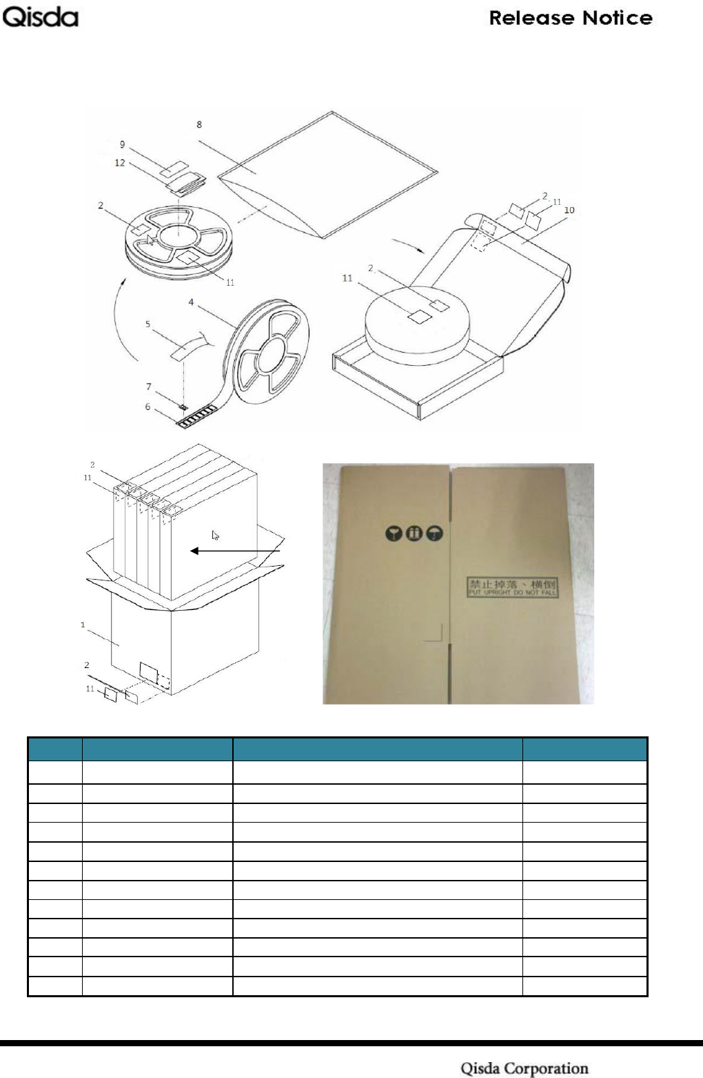
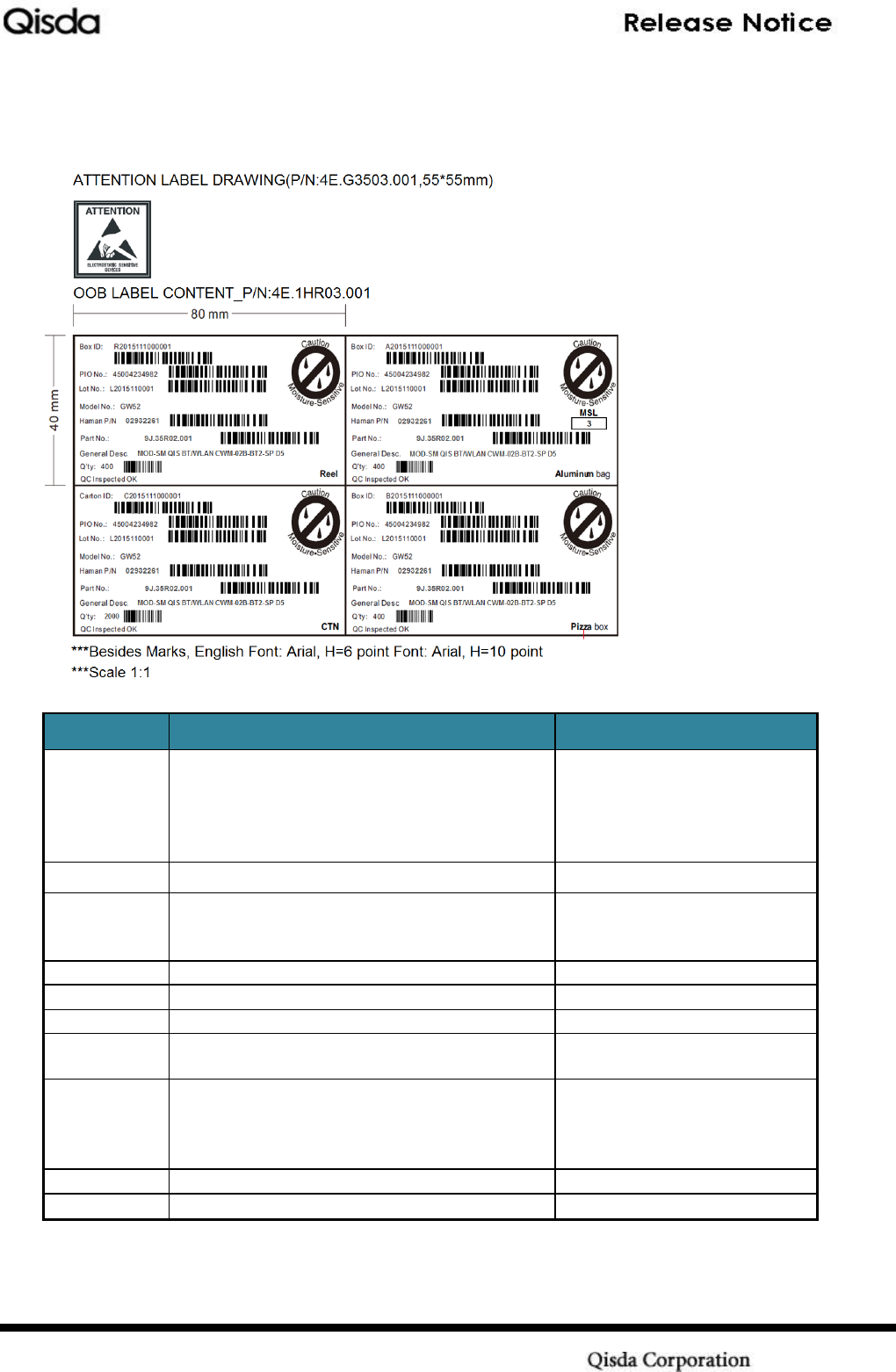
9. PACKING DRAWING
No.
Item
Spec.
Qisda P/N
1
Carton
L355*W340*T386mm (pizza box * 5)
4D.1HR02.001
2
OOB Label
80 * 40 mm
4E.1HR03.001
3
Carton Label
80 * 40 mm
4E.1HR03.001
4
Caution Label
55 mm* 55mm Label Attention 56M31
4E.G3503.001
5
Taping Reel
PLATE Taping reel 13IN.
4B.1HR02.001
6
Cover Tap
COVER TAPE
4B.1HR01.001
7
Carrier Tap
CARRIER TAPE
4B.1HR03.001
8
Module
GW52
9J.35R02.001
9
Aluminum Bag
L460*W410*T0.15mm ALUMINUM BAG
4G.1HR01.001
10
Humidity Indicator
CARD HUMINITY INDICATOR GP
4J.G3501.002
11
Pizza Box
L356*W344*T61 mm
4D.1HR01.001
12
Desiccant Bag
Desiccant Bag 68 * 89
3H.09005.001
Product System (PS)
Form No: QTY0-0B-008-05(120104)
24
10. PACKING LABEL DRAWING
Item
Content
Remark
Reel ID
X code (R/A/B/C) + Year + Month + SN
R = Reel
A = Aluminum bag
B = Pizza box
C = Carton
SN is from 0001 ~ 9999
Ex: R2016120001
P/O No
Defined by Harman
Lot No
L + Year + Month + SN
(a) 5 pizza boxes are in 1 Lot.
(b) SN is from 0001 ~ 9999
Ex: L2016120001
Model No
GW52
Qisda Model No.
Harman P/N
02932261
Defined by Harman
Part No
9J.35R02.001
Qisda Part No.
General
Desc.
MOD-SM QIS BT/WLAN CWM-02B-BT2-SP
D5
Quantity
400 pcs for each Reel
400 pcs for each Aluminum bag
400 pcs for each Pizza box
2000 pcs for each Carton
Quantity depend on real
shipment quantity
EC
01
Started at 01
MSL
Level 3

Product System (PS)
Form No: QTY0-0B-008-05(120104)
25
11. CERTIFICATIONS
11.1. FCC Regulations:
This device complies with part 15 of the FCC Rules. Operation is subject to the
following two conditions: (1) This device may not cause harmful interference, and
(2) this device must accept any interference received, including interference that
may cause undesired operation.
This device has been tested and found to comply with the limits for a Class B digital
device, pursuant to Part 15 of the FCC Rules. These limits are designed to provide
reasonable protection against harmful interference in a residential installation. This
equipment generates uses and can radiate radio frequency energy and, if not
installed and used in accordance with the instructions, may cause harmful
interference to radio communications. However, there is no guarantee that
interference will not occur in a particular installation If this equipment does
cause harmful interference to radio or television reception, which can be
determined by turning the equipment off and on, the user is encouraged to try to
correct the interference by one or more of the following measures:
-Reorient or relocate the receiving antenna.
-Increase the separation between the equipment and receiver.
-Connect the equipment into an outlet on a circuit different from that to which the
receiver is connected.
-Consult the dealer or an experienced radio/TV technician for help.
Changes or modifications not expressly approved by the party responsible for
compliance could void the user‘s authority to operate the equipment.
RF Exposure Information
This Modular Approval is limited to OEM installation for mobile and fixed
applications only. The antenna installation and operating configurations of this
transmitter, including any applicable source-based time-averaging duty factor,
antenna gain and cable loss must satisfy MPE categorical Exclusion Requirements
of §2.1091.
The antenna(s) used for this transmitter must be installed to provide a separation
distance of at least 20 cm from all persons, must not be collocated or operating in
conjunction with any other antenna or transmitter, except in accordance with FCC
multi-transmitter product procedures.

Product System (PS)
Form No: QTY0-0B-008-05(120104)
26
The end user has no manual instructions to remove or install the device and a
separate approval is required for all other operating configurations, including
portable configurations with respect to 2.1093 and different antenna configurations.
This project uses monopole antenna for testing only, so the antenna type limitation.
The antenna gain limits 2dBi. When the module is installed in the host device, the
FCC ID label must be visible through a window on the final device or it must be
visible when an access panel, door or cover is easily re-moved. If not, a second
label must be placed on the outside of the final device that contains the following
text: “Contains FCC ID: VRSGW52”.
12. CONTACT
Qisda Corporation
No.157,Shanying Rd., Gueishan Dist.,
Taoyuan City 333, Taiwan
Tel: +886 3 359 5000-2987
Fax: +886 3 359 3387
Website: Qisda.com