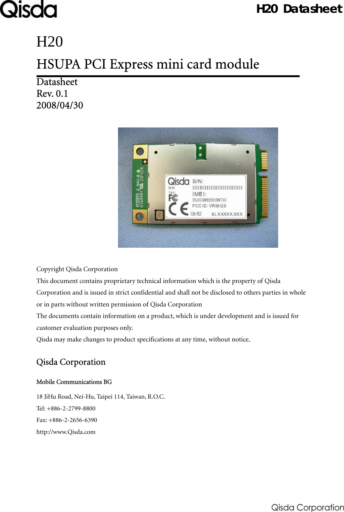
Qisda H20 HSUPA PCI Express mini card module User Manual H20 Manual 2

Qisda Corporation HSUPA PCI Express mini card module H20 Manual 2

UserMan 20090313

  Datasheet H20 HSUPA PCI Express mini card module   Datasheet Rev. 0.1 2008/04/30               Copyright Qisda Corporation This document contains proprietary technical information which is the property of Qisda Corporation and is issued in strict confidential and shall not be disclosed to others parties in whole or in parts without written permission of Qisda Corporation The documents contain information on a product, which is under development and is issued for customer evaluation purposes only.   Qisda may make changes to product specifications at any time, without notice.  Qisda Corporation Mobile Communications BG 18 JiHu Road, Nei-Hu, Taipei 114, Taiwan, R.O.C. Tel: +886-2-2799-8800 Fax: +886-2-2656-6390 http://www.Qisda.com     H20 Datasheet
  HISTORY Version Date  Notes VER: 0.1  2008-APR-30  FIRST RELEASE
   1. INTRODUCTION .................................................................................................... 4 1.1 Description.............................................................................................................4 1.2 Application Device .................................................................................................4 2. FEATURES ............................................................................................................... 5 2.1 General Characteristics ..........................................................................................5 2.2 RF Functionalities ..................................................................................................6 Maximum TX Power............................................................................................6 Parametric Performance ......................................................................................6 Sensitivity.............................................................................................................7 Radio Frequency ..................................................................................................7 3. HARDWARE DESCRIPTION................................................................................... 10 3.1 System Interface....................................................................................................10 3.2 Functional Diagram .............................................................................................11 3.3 Pin Description ....................................................................................................12 3.4 Terminal Definition..............................................................................................14 3.5 Electrical Characteristics ......................................................................................16 DC characteristics ..............................................................................................16 Digital interface..................................................................................................17 USB Transceiver DC characteristics ...................................................................17 USIM Interface...................................................................................................18 3.6 Environmental......................................................................................................19 3.7 Physical Package ...................................................................................................20 4. SOFTWARE CHARACTERISTICS............................................................................ 23 4.1 Introduction .........................................................................................................23 4.2 Software Architecture ...........................................................................................23
  1. INTRODUCTION 1.1 Description Overview This document describes all the functions, features, and interfaces of the HSUPA PCI Express Mini Card Module – H20 from Qisda. Qisda H20 HSUPA module supports Tri-band WCDMA/HSDPA/HSUPA and Quad-band GSM/GPRS/EDGE network connection capability. Qisda H20 HSUPA card can provides high speed data connection, the data speed of downlink and uplink path is up to 7.2Mbps and 5.76Mbps respectively. Furthermore, users can ease to use this module by using the “HMTool” application software that we provide for Windows XP and Vista system. With the Qisda H20 HSUPA module, devices are enhanced in both functionality and usability based on state of the art wireless technology.  1.2 Application Device Scope Qisda H20 module is a high speed modem card with PCI Express minicard form factor and is focusing on the Notebook, UMPC, MID and other portable device marketing.  ¾ Notebook  ¾ Ultra Mobile PC  ¾ Mobile Internet Device  ¾ Wireless Router  ¾ USB Modem  ¾ Car Embedded System
  2. FEATURES  2.1 General Characteristics z Bands: Tri Band WCDMA and Quad Band GSM Band  TX  RX GSM850 824~849 MHz 869~894MHz EGSM900 880~915 MHz  925~960MHz DCS1800 1710~1785MHz 1805~1880MHz PCS1900 1850~1910MHz 1930~1990MHz WCDMA850 824~849 MHz  869~894MHz WCDMA1900 1850~1910MHz  1930~1990MHz WCDMA2100 1920~1980MHz  2110~2170MHz  z Support SIM Interface: 1.8V/3V z Form factor   i. Dimension: 50.95 x 30 x 5.0 mm   ii. Weight: 12g z Power Operation Voltage: 3.3V +/- 9% z Power Consumption: Speech Mode: Band  Typ  Max  Unit GSM850 / PCL=5  385  410  mA EGSM900 / PCL=5  385  410  mA DCS / PCL=0  330  350  mA PCS / PCL=0  330  350  mA WCDMA (all band)  750  820  mA  Standby Mode:  Typ (Average)  Max (Average)  Unit GSM / Page frame=2  3.5  4.5  mA GSM / Page frame=9  1.5  3  mA DCS / Page frame=2  3.5  4.5  mA DCS / Page frame=9  1.9  3.5  mA PCS / Page frame=2  3.5  4.5  mA PCS / Page frame=9  1.6  3  mA WCDMA / DRX=6 (0.64 S)  4.2  5.5  mA WCDMA / DRX=9 (5.12 S)  1.7  3  mA
  z Hardware Interface: 52 Pins PCI Express Mini Card connector interface 2 RF Antenna Coaxial Connectors z Software Interface: USB driver HMTool software tool.    2.2 RF Functionalities Maximum TX Power The performance of the transmitter meets test requirement ETSI TS 151 010-1 chapter 13.3 for GSM, chapter 13.17.3 for EDGE and TS 34.121 chapter 5.2&5.4.3 for WCDMA, chapter 5.2A for HSDPA, chapter 5.2B for HSUPA. Band  Max  Min GSM850  33 dBm ±2dBm  5 dBm ±5dBm EGSM  33 dBm ±2dBm  5 dBm ±5dBm DCS  30 dBm ±2dBm  0 dBm ±5dBm PCS  30 dBm ±2dBm  0 dBm ±5dBm GSM850(EDGE)  27 dBm ±3dBm  5 dBm ±5dBm EGSM(EDGE)  27 dBm ±3dBm  5 dBm ±5dBm DCS(EDGE)  26 dBm ±3dBm  2 dBm ±5dBm PCS(EDGE)  26 dBm ±3dBm  2 dBm ±5dBm UMTS-2100  24 dBm +1/-3dBm  Less than -50dBm UMTS-1900  24 dBm +1/-3dBm  Less than -50dBm UMTS-850  24 dBm +1/-3dBm  Less than -50dBm 1/15≦βo/βd≦12/15 (HS-DPCCH)  24 dBm +1/-3dBm   13/15≦βo/βd≦15/8 (HS-DPCCH)  23 dBm +2/-3dBm   15/7≦βo/βd≦15/0 (HS-DPCCH)  22 dBm +3/-3dBm   Sub-test 1 (E-DCH)  24 dBm +1.7/-5.2dBm   Sub-test 2 (E-DCH)  22 dBm +3.7/-5.2dBm   Sub-test 3 (E-DCH)  23 dBm +2.7/-5.2dBm   Sub-test 4 (E-DCH)  22 dBm +3.7/-5.2dBm   Sub-test 5 (E-DCH)  24 dBm +1.7/-5.2dBm    Parametric Performance Tests carried out at -20ºC, 25ºC and 60ºC for each voltage 3V, 3.3V and 3.6V. The Measured Peak Phase, RMS Phase, frequency error, power level, and static sensitivity meets ETSI TS 151 010-1 chapter 13.1 for GSM and TS 34.121 chapter 5.13.1 for WCDMA, chapter 5.13.1A for HSDPA Band (GSM)  Peak Phase Error  RMS Phase Error GSM850 <20° <5° EGSM <20° <5° DCS <20° <5° PCS <20° <5°
  Band (GSM)  Peak Phase Error  RMS Phase Error Band (WCDMA)  Error Vector Magnitude   UMTS-2100(HS-DPCCH) <17.5%   UMTS-1900(HS-DPCCH) <17.5%   UMTS-850(HS-DPCCH) <17.5%    Sensitivity The performance of the receiver meets test requirement ETSI TS 151 010-1 chapter 14.2.1 for GSM, chapter 14.18.1 for EDGE and TS 34.121 chapter 6.2 for WCDMA.  Band  Typical  Min GSM850  -107 dBm  -104 dBm EGSM  -107 dBm  -104 dBm DCS  -107 dBm  -103 dBm PCS  -107 dBm  -103 dBm EDGE(GMSK modulation)  -107 dBm  -104 dBm EDGE(8-PSK modulation)  -104 dBm  -102 dBm UMTS-2100(Primary)  -109 dBm  -106.7 dBm UMTS-2100(Secondary)  -109 dBm  N/A UMTS-1900(Primary)  -107 dBm  -104.7 dBm UMTS-1900(Secondary)  -109 dBm  N/A UMTS-850(Primary)  -109 dBm  -106.7 dBm UMTS-850(Secondary)  -109 dBm  N/A  Radio Frequency GSM850 (850 MHz) Frequency Range  TX 824-849 MHz; RX 869-894 MHz Channel Spacing  200 KHz Number of Channels  124 Carriers x 8 (TDMA) Modulation  GMSK / 8-PSK Duplex Spacing  45 MHz Frequency Stability  +/- 0.1 ppm (Uplink TX) Power Output  33 dBm Class 8 (2 W peak) – 5 dBm Output Impedance  50 Ohm Spurious Emission  -36 dBm up to 1 GHz (< -30 dBm > 1 GHz) EGSM (900 MHz) Frequency Range  TX 880-915 MHz; RX 925-960 MHz Channel Spacing  200 KHz Number of Channels  124 Carriers x 8 (TDMA) Modulation  GMSK / 8-PSK Duplex Spacing  45 MHz Frequency Stability  +/- 0.1 ppm (Uplink TX) Power Output  33 dBm Class 8 (2 W peak) – 5 dBm Output Impedance  50 Ohm Spurious Emission  -36 dBm up to 1 GHz (< -30 dBm > 1 GHz)
  DCS (1800 MHz) Frequency Range  TX 1710-1785 MHz; RX 1805-1880 MHz Channel Spacing  200 KHz Number of Channels  374 Carriers x 8 (TDMA) Modulation  GMSK / 8-PSK Duplex Spacing  95 MHz Frequency Stability  +/- 0.1 ppm (Uplink TX) Power Output  30 dBm – 0 dBm Output Impedance  50 Ohm Spurious Emission  -36 dBm up to 1 GHz (< -30 dBm > 1 GHz) Compatible with phase 2 feature PCS (1900 MHz) Frequency Range  TX: 1850~1910MHz; RX: 1930~1990MHz Channel Spacing  200KHz Number of Channels  299 Carriers x 8 (TDMA) Modulation  GMSK / 8-PSK Duplex Spacing  80 MHz Frequency Stability  +/- 0.1 ppm (Uplink TX) Power Output  30 dBm – 0 dBm Output Impedance  50 Ohm Spurious Emission  -36 dBm up to 1 GHz (< -30 dBm > 1 GHz) Compatible with phase 2 feature WCDMA_IMT (2100 MHz) Frequency Range  TX: 1920~1980MHz; RX: 2110~2170MHz Channel Raster  200KHz Number of Channels  299 Carriers x 8 (TDMA) Modulation QPSK Duplex Spacing  190 MHz Frequency Stability  +/- 0.1 ppm (Uplink TX) Power Output  24 dBm +1/-3dBm - less than -50dBm Output Impedance  50 Ohm Spurious Emission  -67dBm(925-935MHz);-79dBm(935-960MHz);-71dBm(1805-1880MHz) ;-60dBm(1845-1880MHz);-41dBm(1885-1920MHz) WCDMA_PCS (1900 MHz) Frequency Range  TX: 1850~1910MHz; RX: 1930~1990MHz Channel Raster  200KHz Number of Channels  299 Carriers x 8 (TDMA) Modulation QPSK Duplex Spacing  80 MHz Frequency Stability  +/- 0.1 ppm (Uplink TX) Power Output  24 dBm +1/-3dBm - less than -50dBm Output Impedance  50 Ohm Spurious Emission   WCDMA_850 (850 MHz) Frequency Range  TX 824-849 MHz; RX 869-894 MHz Channel Raster  200KHz Number of Channels  299 Carriers x 8 (TDMA) Modulation QPSK Duplex Spacing  45 MHz
  Frequency Stability  +/- 0.1 ppm (Uplink TX) Power Output  24 dBm +1/-3dBm - less than -50dBm Output Impedance  50 Ohm Spurious Emission  -60dBm(869-894MHz;1930-1990MHz;2110-2155MHz)
  3. HARDWARE DESCRIPTION  3.1 System Interface The I/O connectors of H20 module are PCI EXPRESS MINI CARD and two RF antenna connectors. Table 3-1 summarizes the 25 signals and 18 power lines that are supported by the PCI Express Mini Card System Interface. Table 3-2 shows the antenna interface. Table 3-1 System Interface Signal Group  Pin no.  Description Power  5  3.3V power source GND 13 Return current path USB  2  USB serial data interface compliant to the USB 2.0 specification PERST#  1  Function reset to the card W_DISABLE#  1  Shutdown the HSDPA module UIM 4 SIM function LED 3 Status indicators  Table 3-2 Antenna interface Signal Group  Connector no.  Description ANT 2 Antenna interface
  3.2 Functional Diagram
  3.3 Pin Description  Pin Signal name  Direction  Description 1 NC    No connect 2 +3.3Vaux  Power  3.3V power source 3 NC    No connect 4 GND  Power  Return current path 5 NC    No connect 6 NC    No connect 7 NC    No connect 8  UIM_PWR  Output  Power source for the USIM 9 GND  Power  Return current path 10  UIM_DATA  Input / Output  USIM data signal 11 NC    No connect 12  UIM_CLK  Output  USIM clock signal 13 NC    No connect 14 UIM_RESET  Output  USIM reset signal 15 GND  Power  Return current path 16 NC    No connect 17 NC    No connect 18 GND  Power  Return current path 19 NC    No connect 20 W_DISABLE#  Input Active low signal. This signal is used by the system to shutdown the HSDPA module. 21 GND  Power  Return current path 22 PERST#  Input  Active low signal. Function reset to the card. 23 NC    No connect 24 +3.3Vaux  Power  3.3V power source 25 NC    No connect 26 GND  Power  Return current path 27 GND  Power  Return current path 28 NC    No connect 29 GND  Power  Return current path 30 NC    No connect 31 NC    No connect
  32 NC    No connect 33 NC    No connect 34 GND  Power  Return current path 35 GND  Power  Return current path 36  USB_D-  Input / Output  USB serial data interface (negative) 37 GND  Power  Return current path 38  USB_D+  Input / Output  USB serial data interface (postive) 39 +3.3Vaux  Power  3.3V power source 40 GND  Power  Return current path 41 +3.3Vaux  Power  3.3V power source 42 LED_WWAN#  Output  Active low signal. WAN status LED driver. 43 GND  Power  Return current path 44 LED_WLAN#  Output  Active low signal. LAN status LED driver. 45 NC    No connect 46 LED_WPAN#  Output  Active low signal. PAN status LED driver. 47 NC    No connect 48 NC    No connect 49 NC    No connect 50 GND  Power  Return current path 51 NC    No connect 52 +3.3Vaux  Power  3.3V power source
  3.4 Terminal Definition  Recommend antenna connect Hirose Coaxial Connectors
   System connector 52 pins PCI Express Mini Card
  3.5 Electrical Characteristics DC characteristics Pin Function/ Name  Direction  Parameter  Min Typ Max Unit 1 NC       2 +3.3Vaux  Power  Power Supply Voltage  3.0  3.3  3.6  V 3 NC       4 GND  Power  Ground   5 NC       6 NC       7 NC       Supply Voltage  1.5  2.85  3.05  V 8 UIM_PWR  Output Current     150    mA 9 GND  Power  Ground   10  UIM_DATA  Input / Output           11 NC       12 UIM_CLK  Output           13 NC       14 UIM_RESET  Output           15 GND  Power  Ground   16 NC       17 NC       18 GND  Power  Ground   19 NC       Logic High Input Voltage  1.69  2.6  3.3  V 20 W_DISABLE#  Input Logic Low Input Voltage  -0.3  0  0.91  V 21 GND  Power  Ground   Logic High Input Voltage  1.69  2.6  3.3  V 22 PERST#  Input Logic Low Input Voltage  -0.3  0  0.91  V 23 NC       24 +3.3Vaux  Power  Power Supply Voltage  3.0  3.3  3.6  V 25 NC       26 GND  Power  Ground   27 GND  Power  Ground   28 NC       29 GND  Power  Ground   30 NC       31 NC
  32 NC       33 NC       34 GND  Power  Ground   35 GND  Power  Ground   36  USB_D-  Input / Output  Termination Voltage  3.0  3.3  3.6  V 37 GND  Power  Ground   38  USB_D+  Input / Output  Termination Voltage  3.0  3.3  3.6  V 39 +3.3Vaux  Power  Power Supply Voltage  3.0  3.3  3.6  V 40 GND  Power  Ground   41 +3.3Vaux  Power  Power Supply Voltage  3.0  3.3  3.6  V 42 LED_WWAN#  Output  Driver current  0    150  mA 43 GND  Power  Ground   44 LED_WLAN#  Output  Driver current  0    150  mA 45 NC       46 LED_WPAN#  Output  Driver current  0    300  mA 47 NC       48 NC       49 NC       50 GND  Power  Ground   51 NC       52 +3.3Vaux  Power  Power Supply Voltage  3.0  3.3  3.6  V  Digital interface Parameter  Min  Typ  Max  Unit Logic High Input Voltage  1.69  2.6  2.9  V Logic Low Input Voltage  -0.3  0  0.91  V Logic High Output Voltage  2.15  2.6  2.6  V Logic Low Output Voltage  -0.3  0  0.45  V  USB Transceiver DC characteristics The USB interface is powered from 3.3V power source. Parameter  Comments  Min  Ty p  Max  Unit Input sensitivity (differential)  |D+-D-|, VIN=0.8 to 2.5V  0.2     V Output voltage Logic LOW Logic HIGH  RL=1.5KΩ to 3.6V RL=1.5KΩ to GND, IO=1mA   2.8   0.3 3.6  V V Series output resistance  D+, D-  28  33  44  Ω
  Internal pull-up resistor  3.3V to D+, 3.3V to D-  1.425  1.5  1.575  KΩ Internal pull-down resistor  D+ to GND, D- to GND  14.3  15  24.8  KΩ  USIM Interface The USIM signals are defined on system connector to provide the interface between the removable User Identity Module. USIM interface usually run off either 1.8V or 3.0V. Pin  Name  Direction  Description 8 UIM_PWR  Output  Power source for the USIM 10  UIM_DATA  Input / Output  USIM data signal 12 UIM_CLK  Output  USIM clock signal 14 UIM_RESET  Output  USIM reset signal  Parameter  Comments  Min  Typ  Max  Unit Logic High Input Voltage   1.8525 2.85  3.15  V Logic Low Input Voltage   -0.3 0 0.9975 V Logic High Output Voltage   2.4 2.85 2.85  V Logic Low Output Voltage   -0.3 0 0.45 V Schmitt Hysteresis    150      mV Logic input leakage current    -200    200  nA Internal pull-up resistor  Programmable range  1    30  KΩ
  3.6 Environmental Operational temperature: -20 ~ +60 ℃ Functional temperature: -20 ~ +70 ℃ Storage temperature: -40 ~ +85 ℃  Note: ¾ The maximum case temperature (Tc) of shielding case cover should be under 90 ℃ (@RF TX power = 24dBm) for ensure all of the characteristics of H20 module can be fulfilled the ETSI specification.  ¾
  3.7 Physical Package Top View
   Bottom View
   Side View
  4. SOFTWARE CHARACTERISTICS  4.1 Introduction We provide the PC Tool – HMTool for H20 HSUPA card. The main functions in this tool are Contacts (only SIM card), SMS, Settings, and Network Management.  4.2 Software Architecture
-28- FEDERAL COMMUNICATIONS COMMISSION INTERFERENCE STATEMENT  This mobile device meets guidelines for exposure to radio waves. Your mobile device is a radio transmitter and receiver. It is designed not to exceed the limits for exposure to radio waves recommended by international guidelines.  This equipment has been tested and found to comp ly with the limits for a Class B digit al device, pursuant to P art 15 of the FCC Ru les. Thes e limit s are  designed to provide  reasonable protection against harmful interfer ence in a residential inst allation. This equipment generates, uses and c an radiate radio frequency energy  and, if not inst alled and used in accordance with the instructions,  may cause harmful  interference to radio communications. However , there is no guarant ee that interference will not occur in a particular inst allation. If this equipment  does cause harmful i nterference to radio or television reception, which c an be determined  by turning the equipment of f and on, th e user is encouraged to try to  correct the interference by one  or more of the following  measures: –  Reorient or relocate the receiving antenna. –  Increase the separation between the equipment and receiver. –  Connect the equipment into an outlet on a circ uit dif ferent from that to w hich the receiver is connected. –  Consult the dealer or an experienced radio/TV technician for help. CAUTION: Any changes or modifications not expre ssly approved by the p arty responsible for compliance could void the user's authority to operate the equipment.   FCC RF Radiation Exposure Statement This equipment complies with F CC RF radiation  exposure limits set forth for an uncontrolled environment. This equipment must be inst alled and operated with a minimum dist ance of  20cm between the radiator and your body.

Navigation menu