Qisda M27 GSM/GPRS MODULE User Manual USERS MANUAL
Qisda Corporation GSM/GPRS MODULE USERS MANUAL
UserManual.wiki
>
Qisda
>
M27 User Manual
USERS MANUAL
Navigation menu
Upload a User Manual
Namespaces
Wiki Guide
HTML
PDF
Info
Views
User Manual
Discussion / Help
Navigation
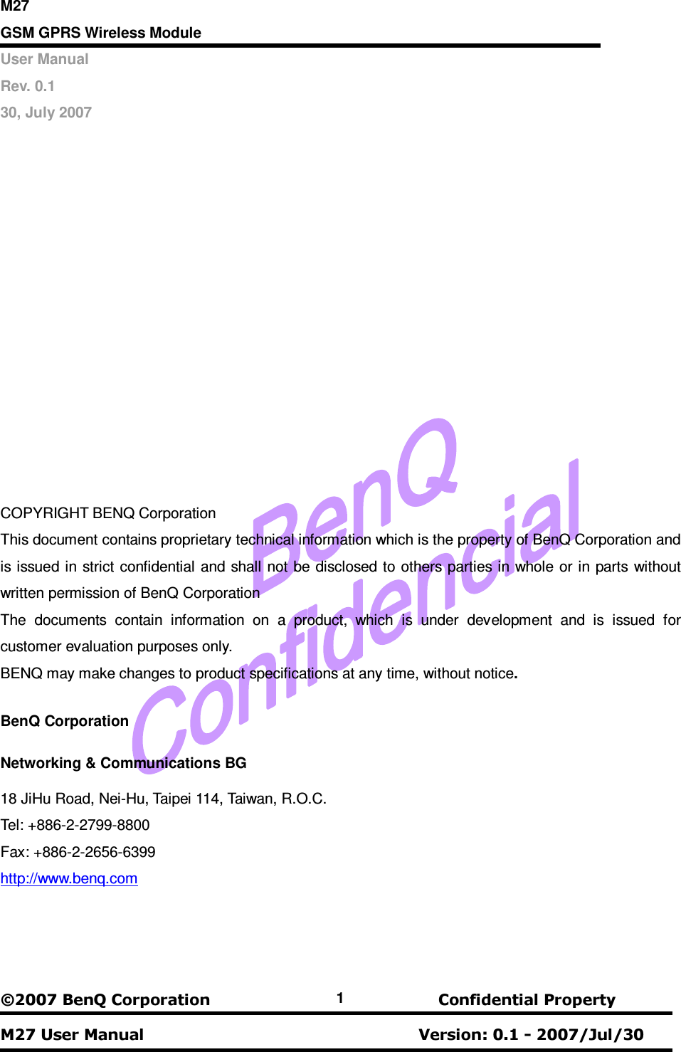
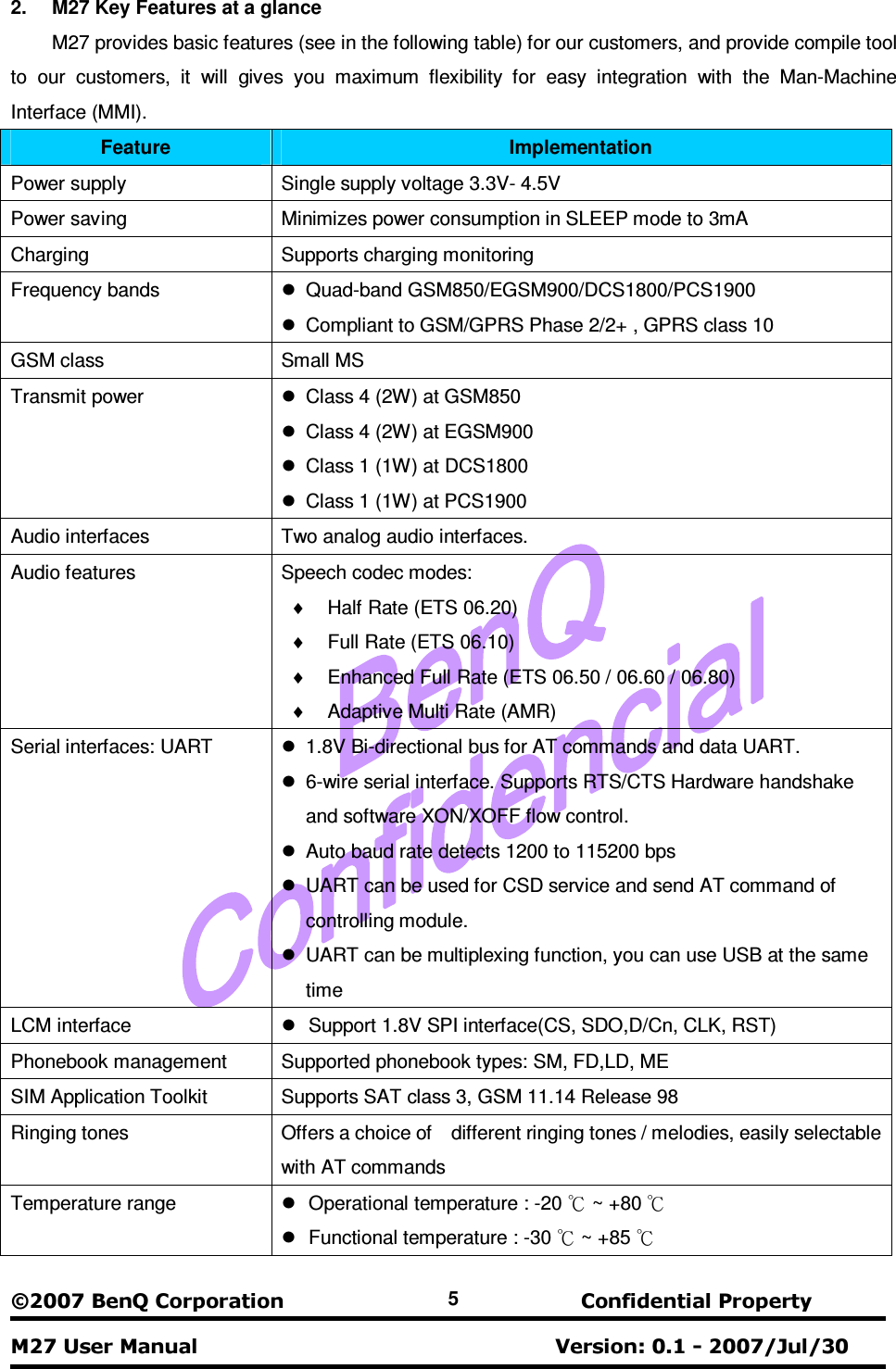
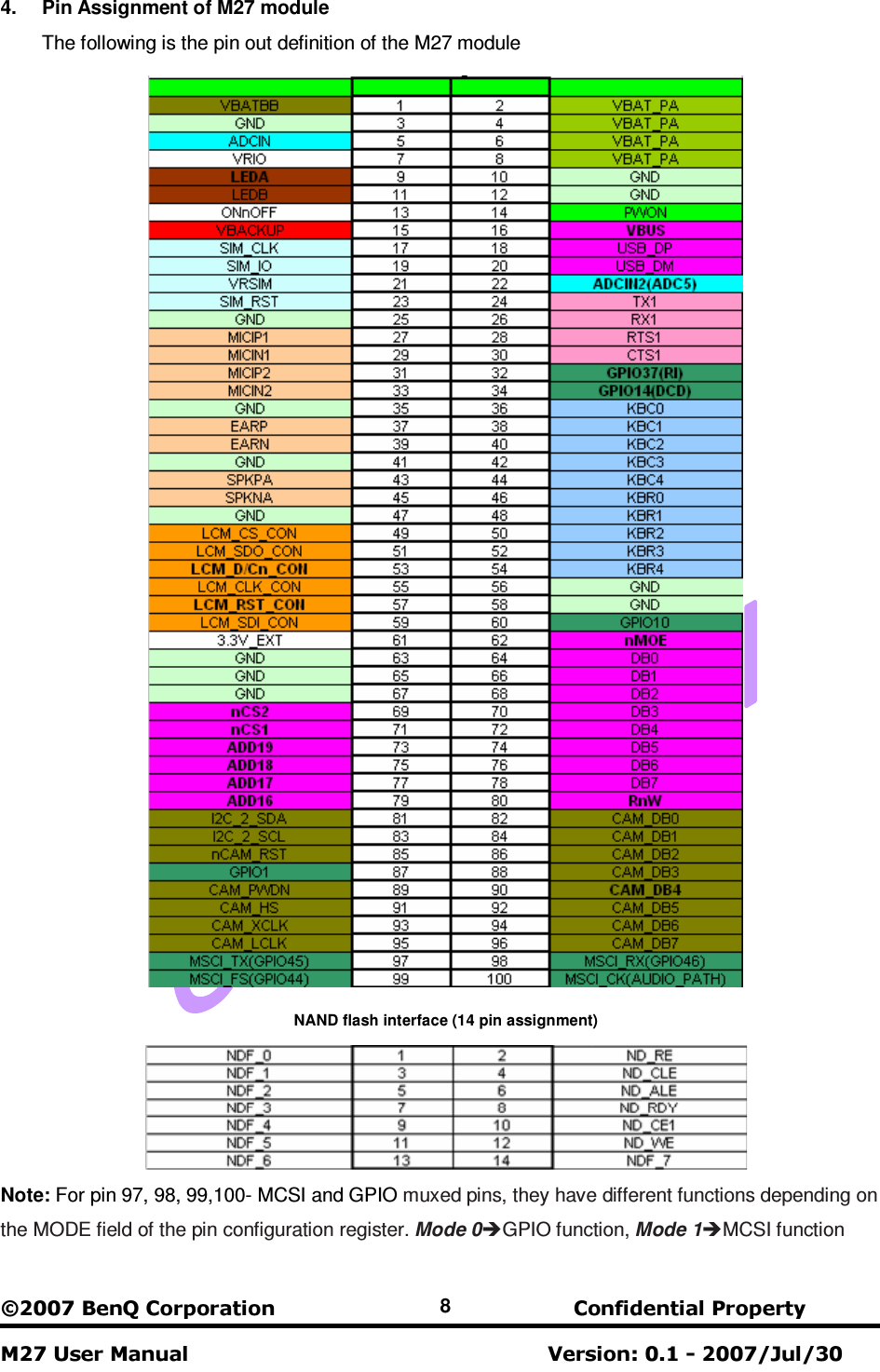
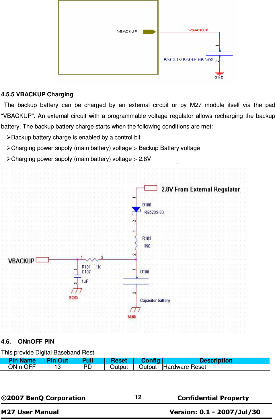
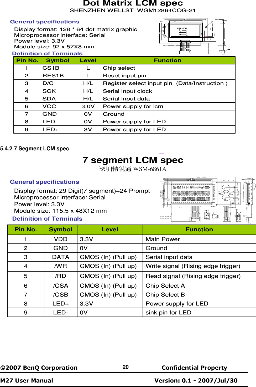
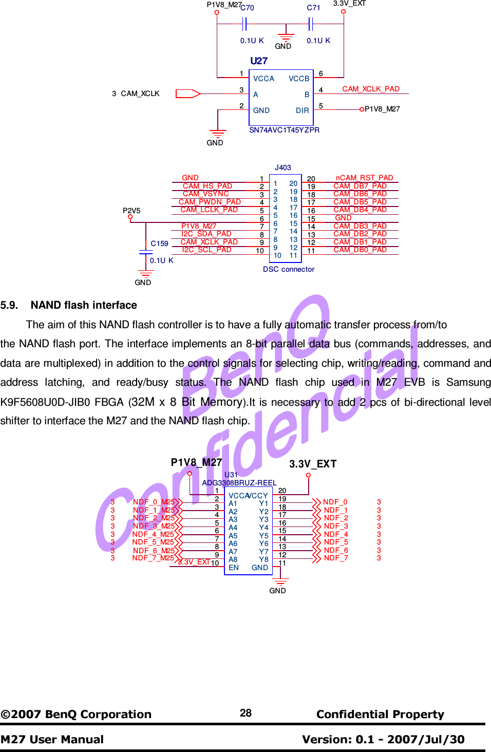
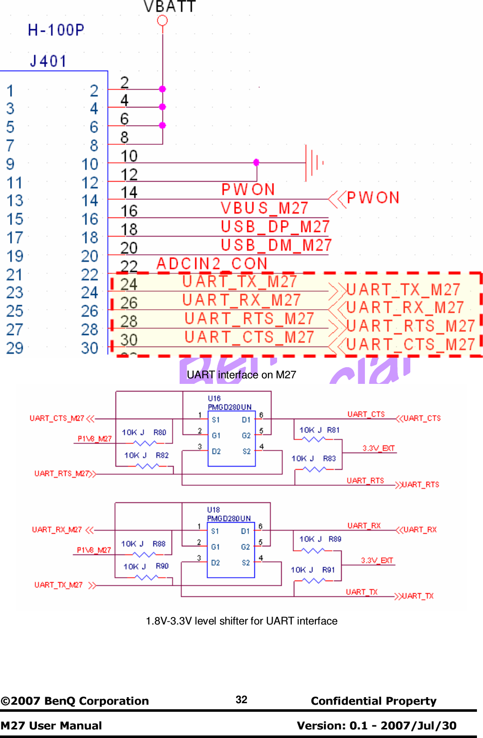
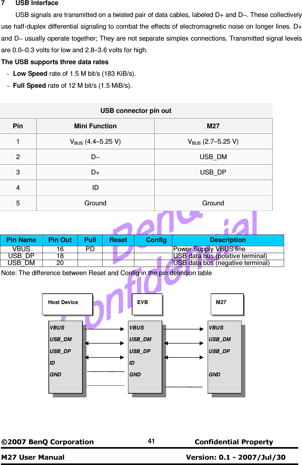
![©2007 B e n Q C o r p o r a t i o n C o n f i d e n t i a l P r o p e r t y M 27 U s e r M a n u a l V e r s i o n : 0. 1 - 2007/ J u l / 3 0 36 U5PMGD280UNS11D23G2 5S2 4G12D1 6UART_RXBUART_TXB3.3V1.8V R1310K JR1210K JR1410K JR1510K JUART_CTSBU6PMGD280UNS11D23G2 5S2 4G12D1 63.3VUART_RSTB1.8V R1910K JR1710K JR2010K JR2110K JU1EXAR XR16M2550 / NXP SC16C852LD330D027D229 D128D532RTSA# 23RXA 4TXA 5VCC 26D431CTSA# 25D61D72A020A119A218IOR#14IOW#12UART_CSA#7UART_CSB#8UART_INTA22UART_INTB21UART_RESET24TXB 6RXB 3RTSB# 15GND13XTAL110XTAL211GND33NC9NC17 CTSB# 16D0D1D4D3D2D6D5D7A0A2A1D[0..7]A[0..2] A[0..2]UART_CSA#IOW#IOR#UART_INTAUART_RESETUART_CSB#UART_INTBR8 0 ohmX124MHz21C722P JC622P JR11576K JD[0..7] 1.8V U2PMGD280UNS11D23G2 5S2 4G12D1 6UART_RXA3.3VUART_TXA1.8V R210K JR110K JR410K JR510K JUART_CTSAU4PMGD280UNS11D23G2 5S2 4G12D1 6UART_RSTA3.3V1.8V R710K JR610K JR910K JR1010K JLevel shifter Dual UART interface EXAR XR16M2550 HIGH PERFORMANCE LOW VOLTAGE DUART WITH 16-BYTE FIFO Package 32 PIN QFN(5x5mm), 48 PIN TQFP (9x9mm)](https://usermanual.wiki/Qisda/M27/User-Guide-872835-Page-36.png)
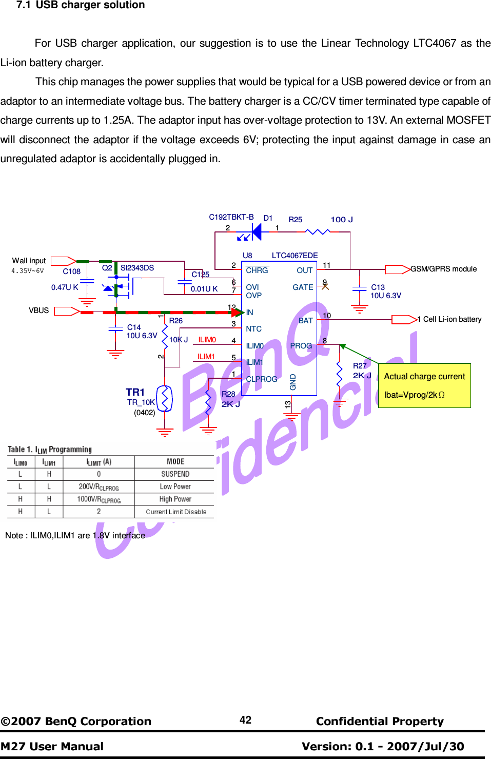
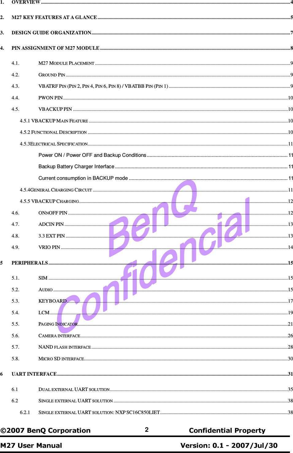
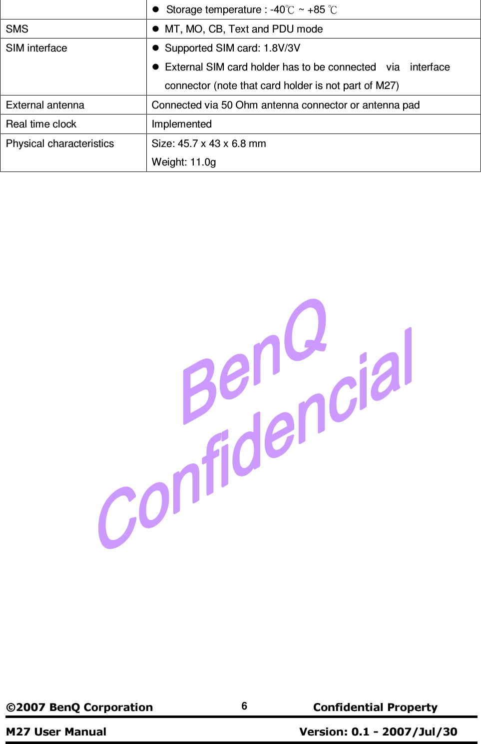
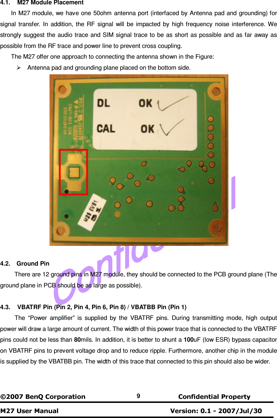
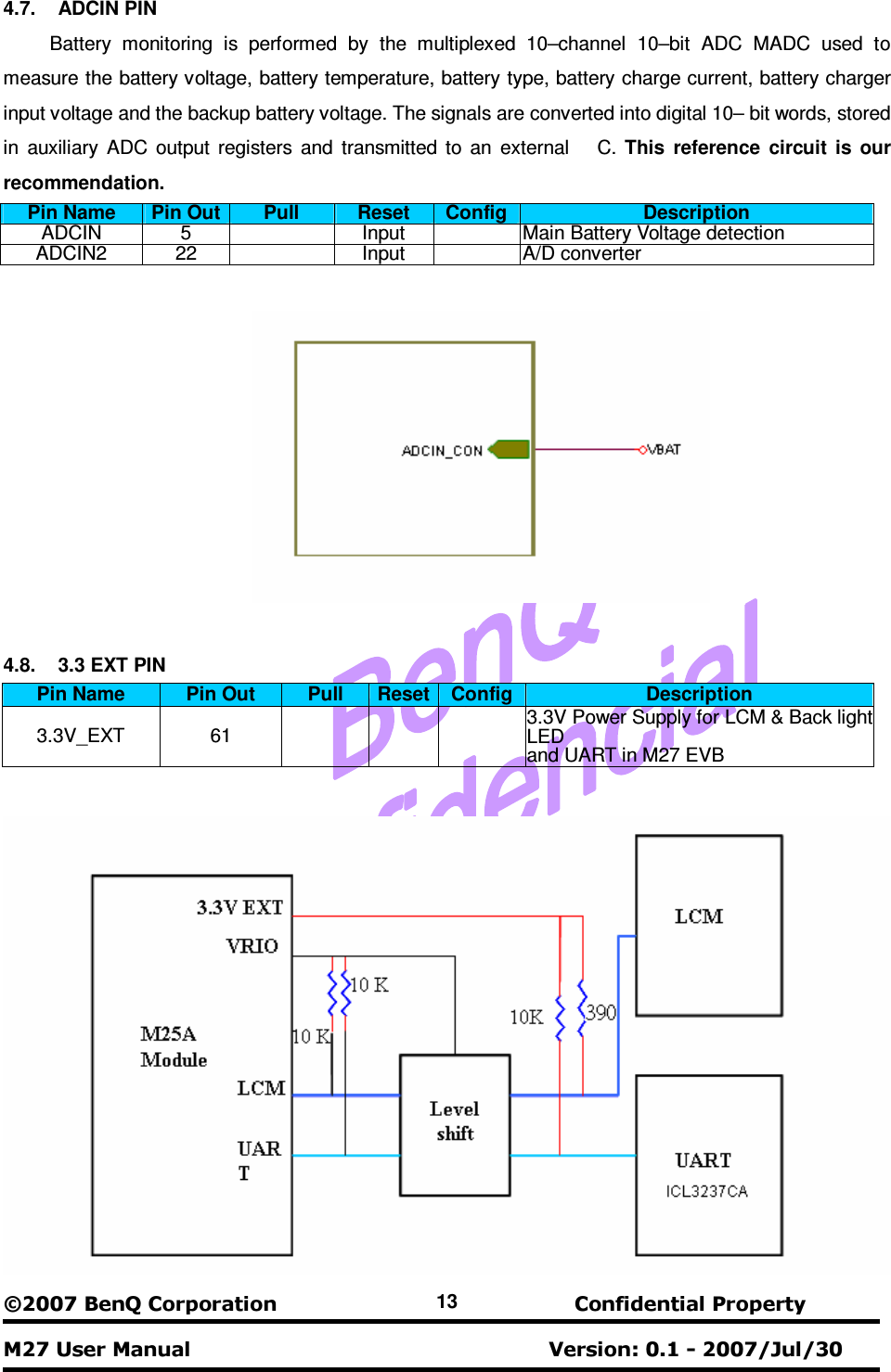
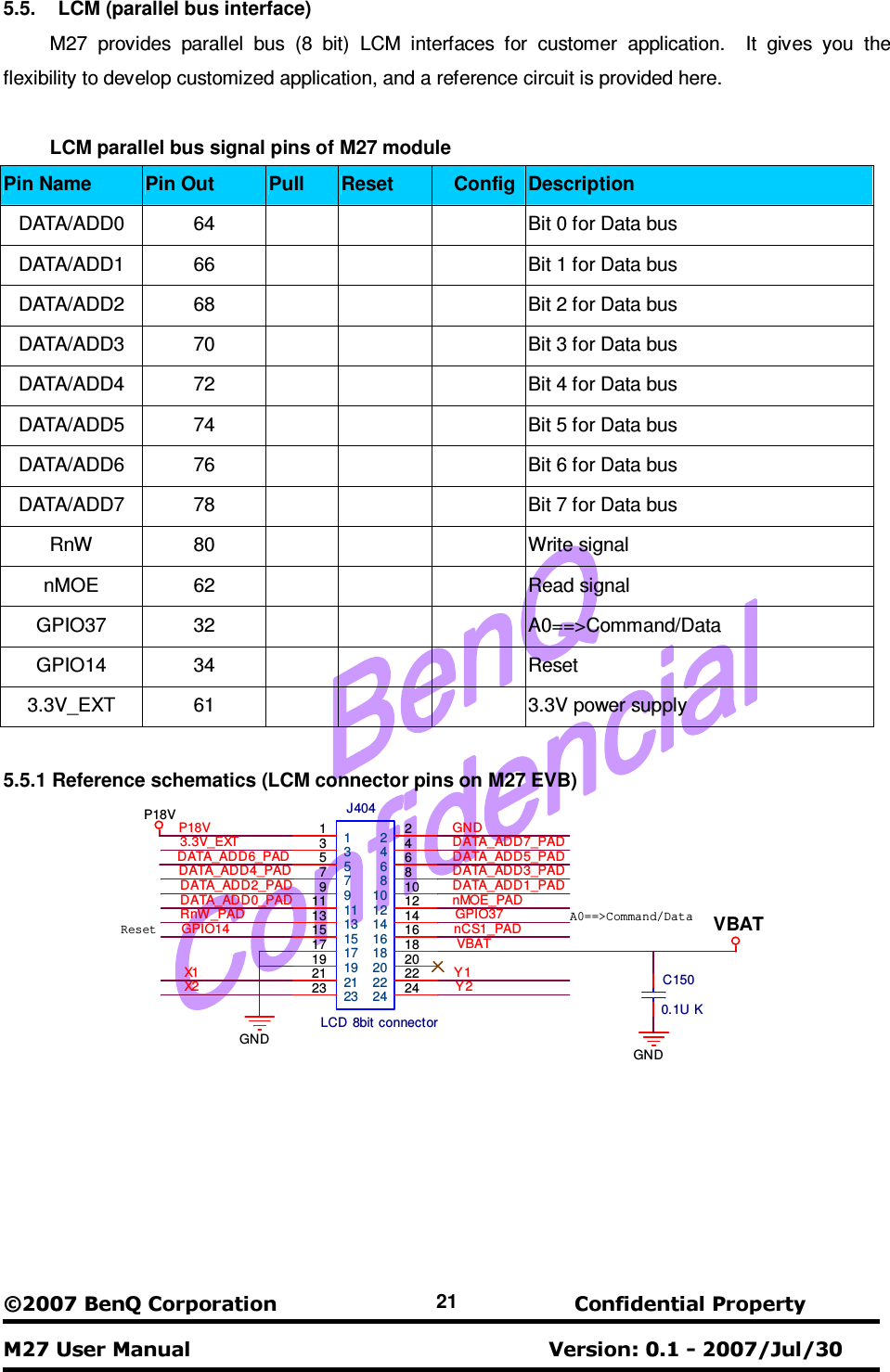
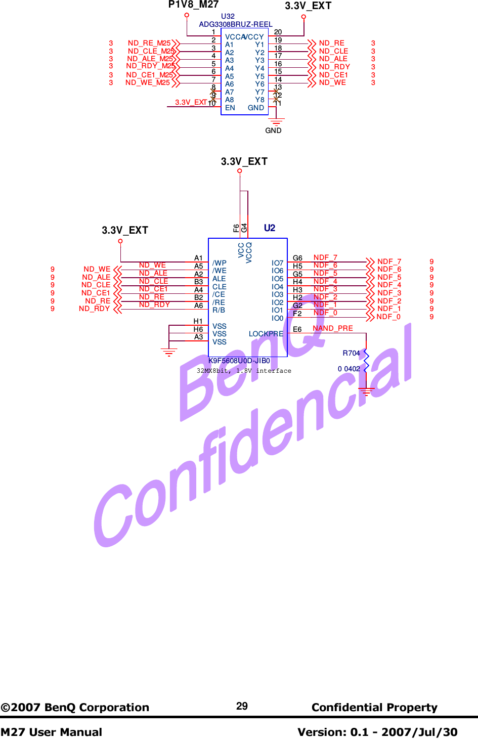
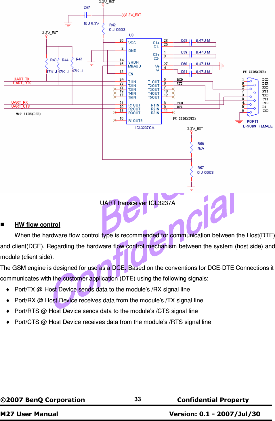
![©2007 B e n Q C o r p o r a t i o n C o n f i d e n t i a l P r o p e r t y M 27 U s e r M a n u a l V e r s i o n : 0. 1 - 2007/ J u l / 3 0 39 U16SC16C850LIETVDD A1N.C. A2IORA3N.C. A4XTAL2A5XTAL1A6A2B1N.C. B2N.C. B3IOWB4LOWPWRB5CSB6A0C1VSSC2A1C3VSSC4TX C5RX C6INTD1RTS D2VDD D4D7D5 D6D6DSR F2N.C. E2CD E3D1E4D3E5D5E6RESETF1DTR E1RI F3D0F4D2F5D4F6CTS D3D0D1D3D2D4D5D7D6A0A1A2D[0..7]A[0..2] A[0..2]D[0..7]IOW#IOR#UART_RESETNote : UART_TXA, UART_RXA, UART_RSTA, UART_CTSA are from M27X324MHz21C2822P JC2722P JR58576K JR57 0 ohmUART_CSA#UART_INTAUART_LOWPWRC220.1U K1.8VUART_RXBU18PMGD280UNS11D23G2 5S2 4G12D1 63.3VUART_TXB1.8V R5210K JR5110K JR5310K JR5410K J](https://usermanual.wiki/Qisda/M27/User-Guide-872835-Page-39.png)
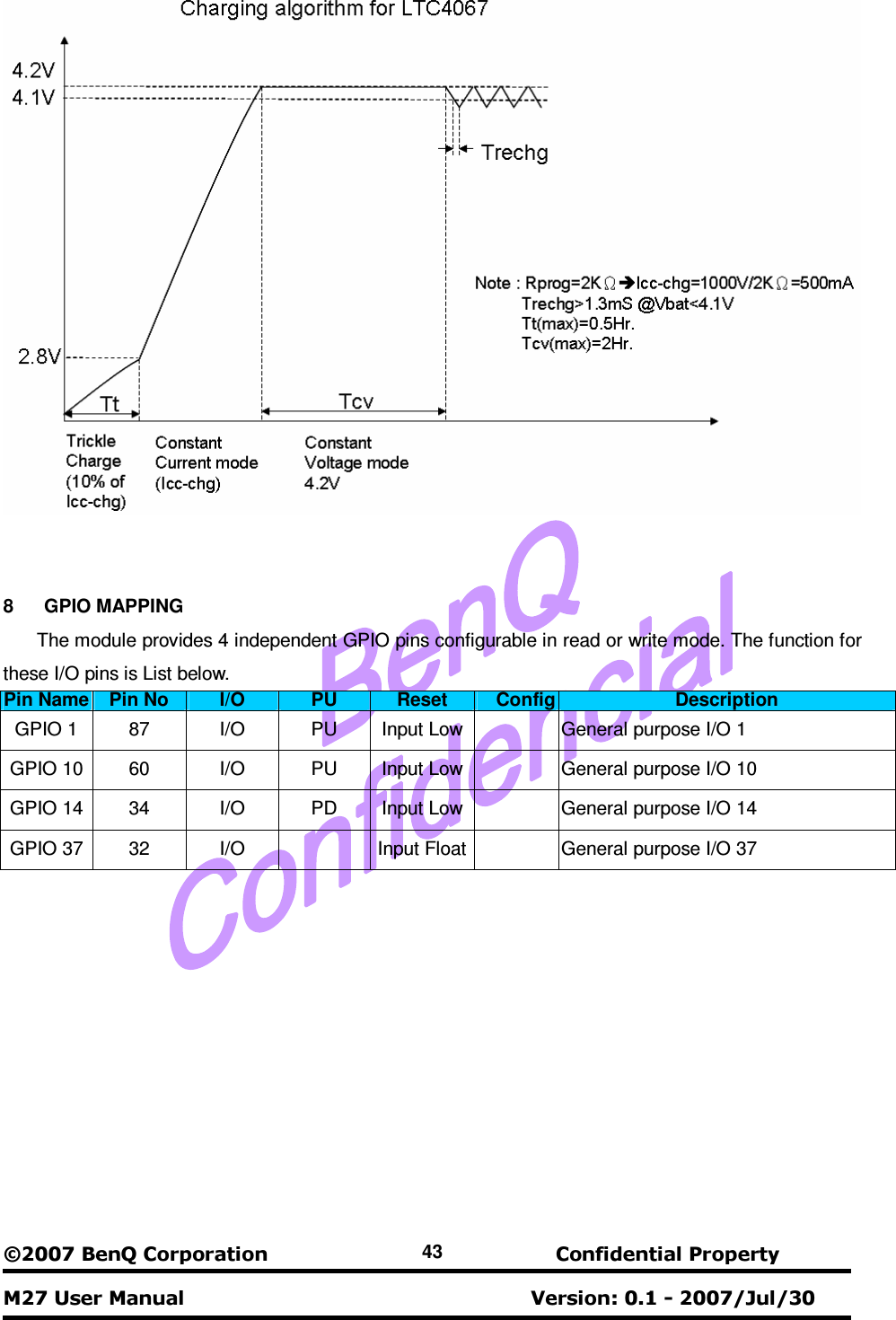
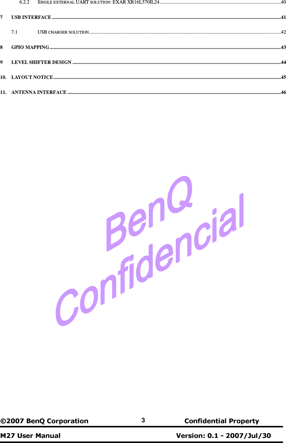
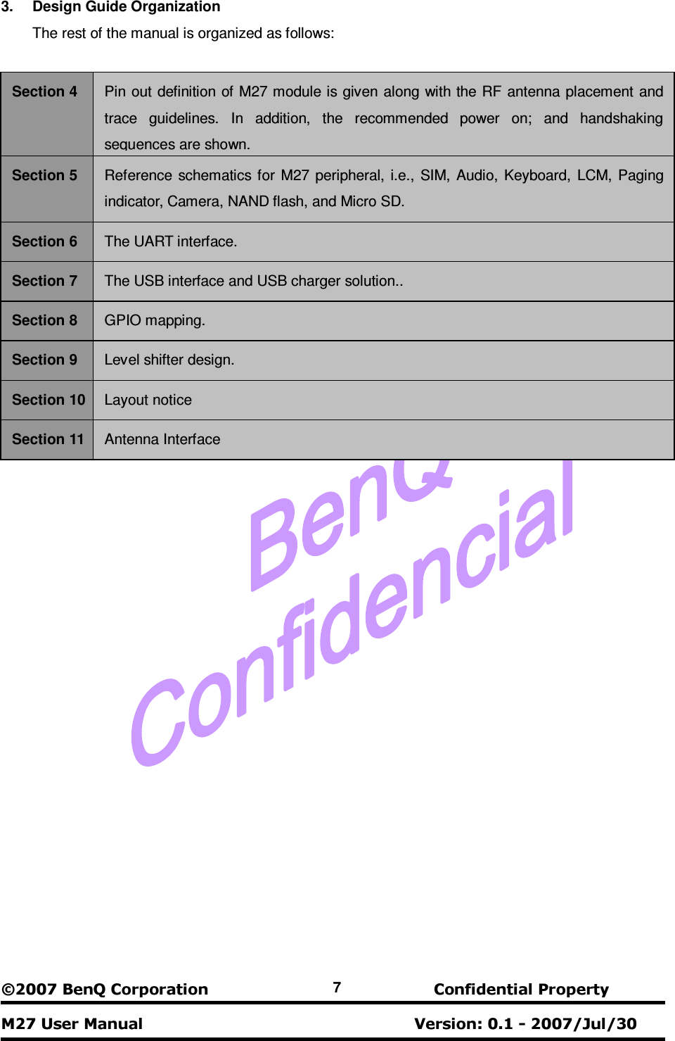
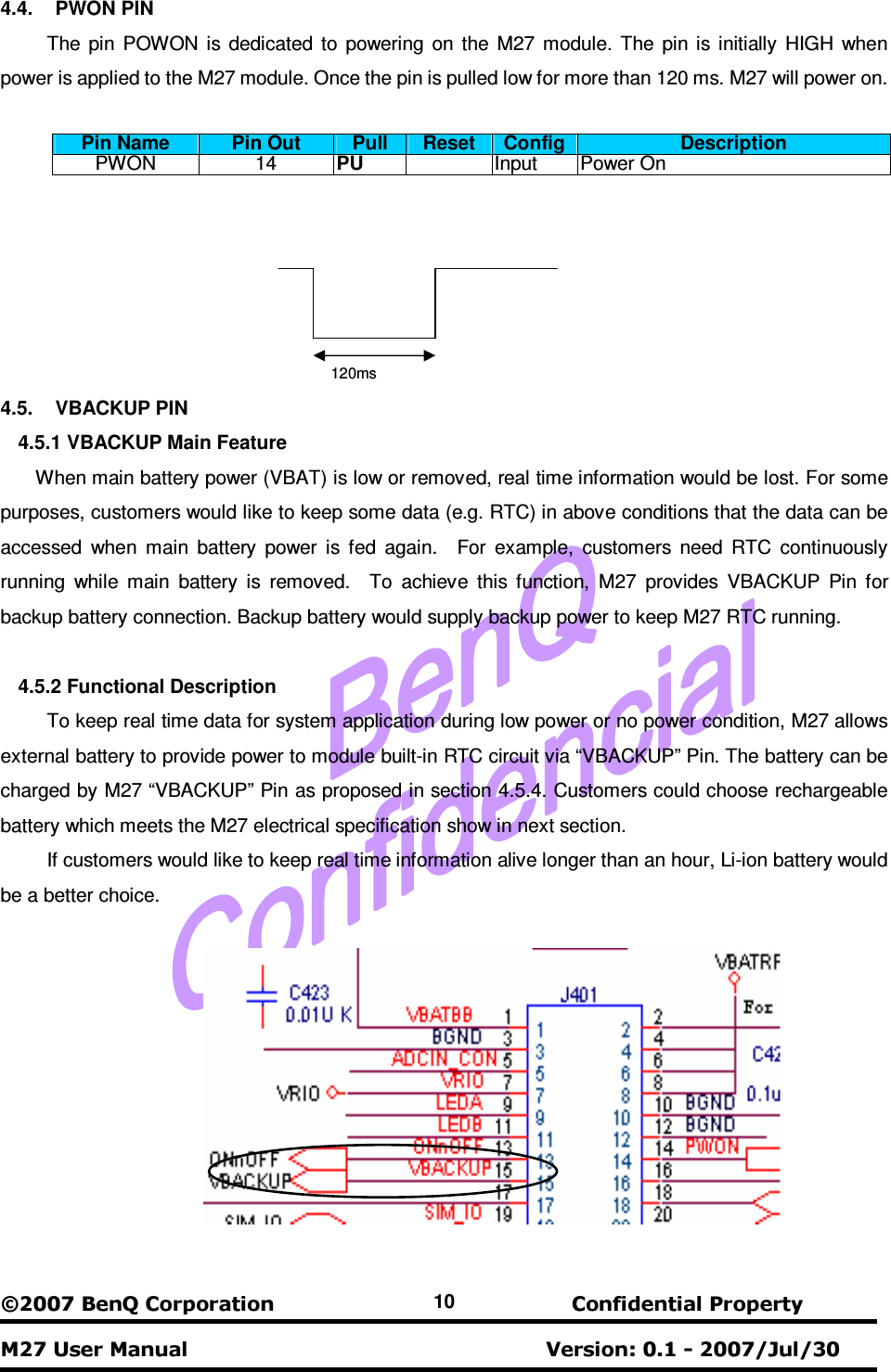
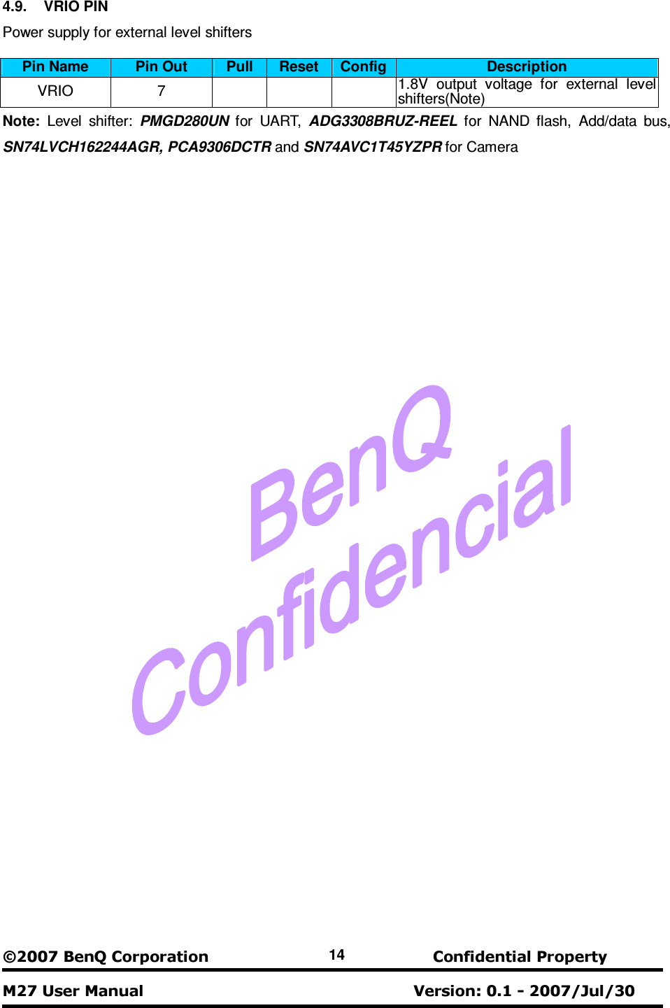
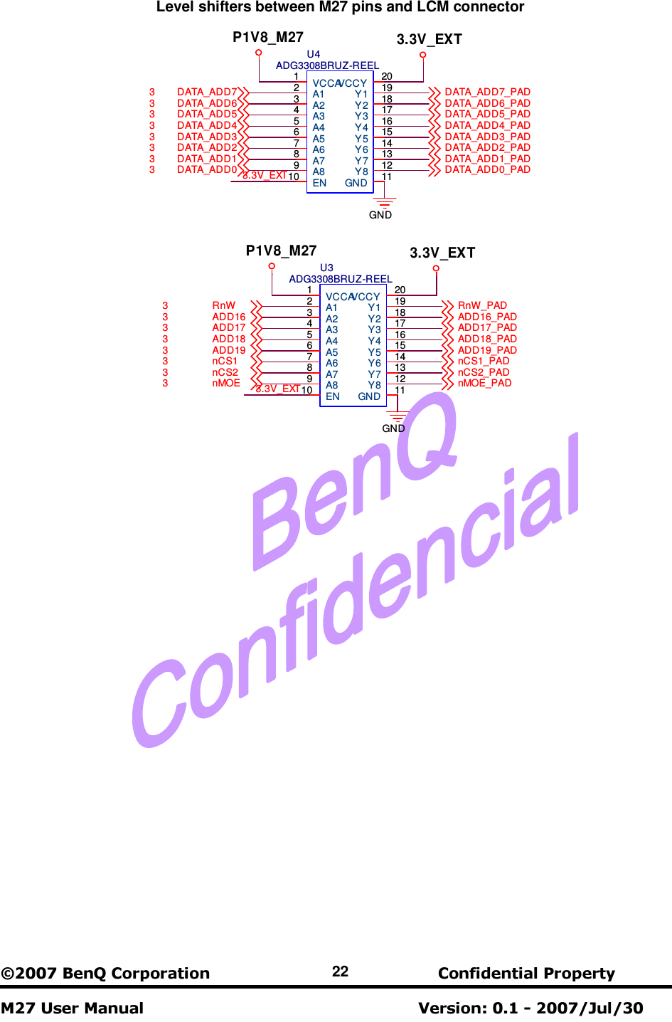
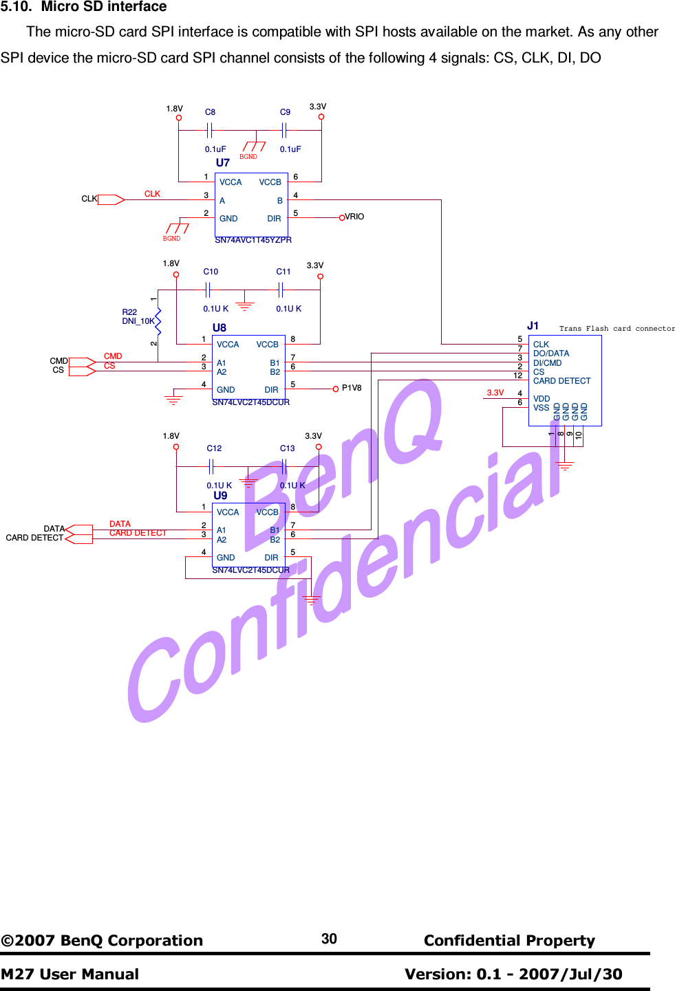
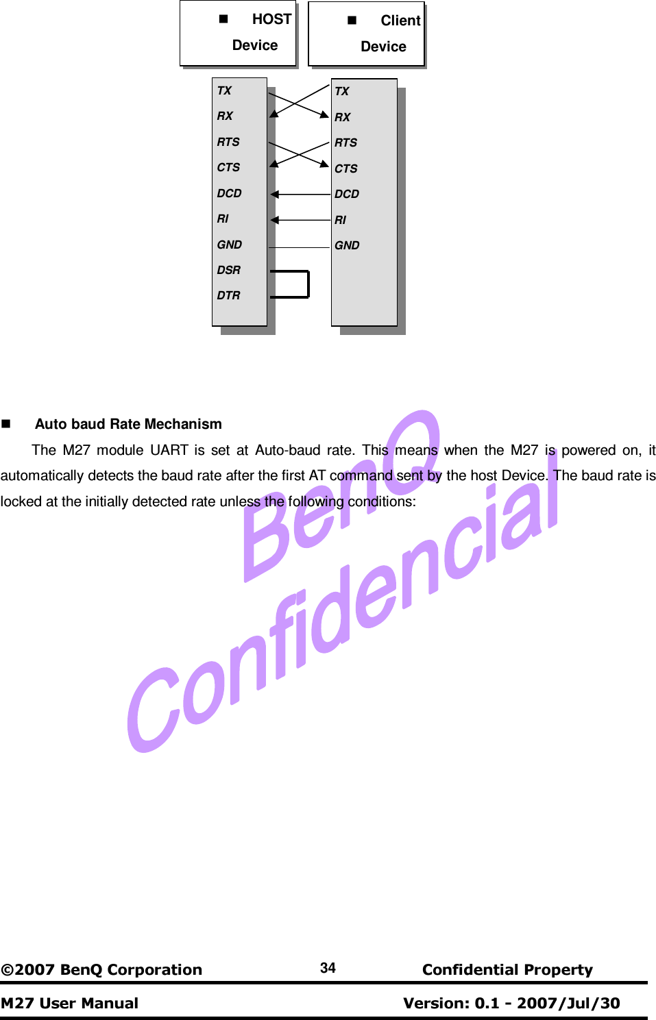
![©2007 B e n Q C o r p o r a t i o n C o n f i d e n t i a l P r o p e r t y M 27 U s e r M a n u a l V e r s i o n : 0. 1 - 2007/ J u l / 3 0 40 6.2.2 Single external UART solution: EXAR XR16L570IL24 UART_INTA1.8VUART_RXBU14PMGD280UNS11D23G2 5S2 4G12D1 63.3VUART_TXB1.8V R4510K JR4410K JR4610K JR4710K JC200.047U KY124MHZCont 1GND2OUT 3VDD4U13 XR16L570IL24D323D020D222 D121D51RXA 4TXA 5VCC 19D424CTS# 18D62D73A014A113A212IOR#11IOW#9UART_CS#6UART_INT15UART_RESET17PwrSave7CLK8GND10RTS# 163.3VD0D1D4D3D2D6D5D7A0A2A1D[0..7]IOR#A[0..2] A[0..2]D[0..7]IOW#UART_CSA#UART_RESETSingle UART interface EXAR XR16L570IL24 SMALLEST 1.62V TO 5.5V UART WITH 16-BYTE FIFO AND POWERSAVE Package 24 PIN QFN(4x4mm), 32 PIN QFN(5x5mm)](https://usermanual.wiki/Qisda/M27/User-Guide-872835-Page-40.png)