Qisda M27 GSM/GPRS MODULE User Manual USERS MANUAL
Qisda Corporation GSM/GPRS MODULE USERS MANUAL
Qisda >
USERS MANUAL

©2007 B e n Q C o r p o r a t i o n C o n f i d e n t i a l P r o p e r t y
M 27 U s e r M a n u a l V e r s i o n : 0. 1 - 2007/ J u l / 3 0
1
M27
GSM GPRS Wireless Module
User Manual
Rev. 0.1
30, July 2007
COPYRIGHT BENQ Corporation
This document contains proprietary technical information which is the property of BenQ Corporation and
is issued in strict confidential and shall not be disclosed to others parties in whole or in parts without
written permission of BenQ Corporation
The documents contain information on a product, which is under development and is issued for
customer evaluation purposes only.
BENQ may make changes to product specifications at any time, without notice.
BenQ Corporation
Networking & Communications BG
18 JiHu Road, Nei-Hu, Taipei 114, Taiwan, R.O.C.
Tel: +886-2-2799-8800
Fax: +886-2-2656-6399
http://www.benq.com

©2007 B e n Q C o r p o r a t i o n C o n f i d e n t i a l P r o p e r t y
M 27 U s e r M a n u a l V e r s i o n : 0. 1 - 2007/ J u l / 3 0
2
1.
OVERVIEW ...........................................................................................................................................................................................................4
2.
M27 KEY FEATURES AT A GLANCE .............................................................................................................................................................5
3.
DESIGN GUIDE ORGANIZATION..................................................................................................................................................................7
4.
PIN ASSIGNMENT OF M27 MODULE ...........................................................................................................................................................8
4.1.
M27
M
ODULE
P
LACEMENT
...............................................................................................................................................................9
4.2.
G
ROUND
P
IN
.......................................................................................................................................................................................9
4.3.
VBATRF
P
IN
(P
IN
2,
P
IN
4,
P
IN
6,
P
IN
8)
/
VBATBB
P
IN
(P
IN
1) ...................................................................................................9
4.4.
PWON
PIN .......................................................................................................................................................................................10
4.5.
VBACKUP
PIN ...............................................................................................................................................................................10
4.5.1
VBACKUP
M
AIN
F
EATURE
..................................................................................................................................................................10
4.5.2
F
UNCTIONAL
D
ESCRIPTION
...................................................................................................................................................................10
4.5.3E
LECTRICAL
S
PECIFICATION
...................................................................................................................................................................11
Γ
Power ON / Power OFF and Backup Conditions......................................................................................................11
Γ
Backup Battery Charger Interface.............................................................................................................................11
Γ
Current consumption in BACKUP mode ................................................................................................................... 11
4.5.4G
ENERAL
C
HARGING
C
IRCUIT
...............................................................................................................................................................11
4.5.5
VBACKUP
C
HARGING
..........................................................................................................................................................................12
4.6.
ON
N
OFF
PIN ...................................................................................................................................................................................12
4.7.
ADCIN
PIN ......................................................................................................................................................................................13
4.8.
3.3
EXT
PIN .....................................................................................................................................................................................13
4.9.
VRIO
PIN .........................................................................................................................................................................................14
5
PERIPHERALS ...................................................................................................................................................................................................15
5.1.
SIM ...................................................................................................................................................................................................15
5.2.
A
UDIO
...............................................................................................................................................................................................15
5.3.
KEYBOARD....................................................................................................................................................................................17
5.4.
LCM..................................................................................................................................................................................................19
5.5.
P
AGING
I
NDICATOR
...........................................................................................................................................................................21
5.6.
C
AMERA INTERFACE
.........................................................................................................................................................................26
5.7.
NAND
FLASH INTERFACE
................................................................................................................................................................28
5.8.
M
ICRO
SD
INTERFACE
......................................................................................................................................................................30
6
UART INTERFACE............................................................................................................................................................................................31
6.1
D
UAL EXTERNAL
UART
SOLUTION
.................................................................................................................................................35
6.2
S
INGLE EXTERNAL
UART
SOLUTION
..............................................................................................................................................38
6.2.1
S
INGLE EXTERNAL
UART
SOLUTION
:
NXP
SC16C850LIET........................................................................................................38

©2007 B e n Q C o r p o r a t i o n C o n f i d e n t i a l P r o p e r t y
M 27 U s e r M a n u a l V e r s i o n : 0. 1 - 2007/ J u l / 3 0
3
6.2.2
S
INGLE EXTERNAL
UART
SOLUTION
:
EXAR
XR16L570IL24 .....................................................................................................40
7
USB INTERFACE ...............................................................................................................................................................................................41
7.1
USB
CHARGER SOLUTION
................................................................................................................................................................42
8
GPIO MAPPING .................................................................................................................................................................................................43
9
LEVEL SHIFTER DESIGN ..............................................................................................................................................................................44
10.
LAYOUT NOTICE..............................................................................................................................................................................................45
11.
ANTENNA INTERFACE ..................................................................................................................................................................................46
©2007 B e n Q C o r p o r a t i o n C o n f i d e n t i a l P r o p e r t y
M 27 U s e r M a n u a l V e r s i o n : 0. 1 - 2007/ J u l / 3 0
4
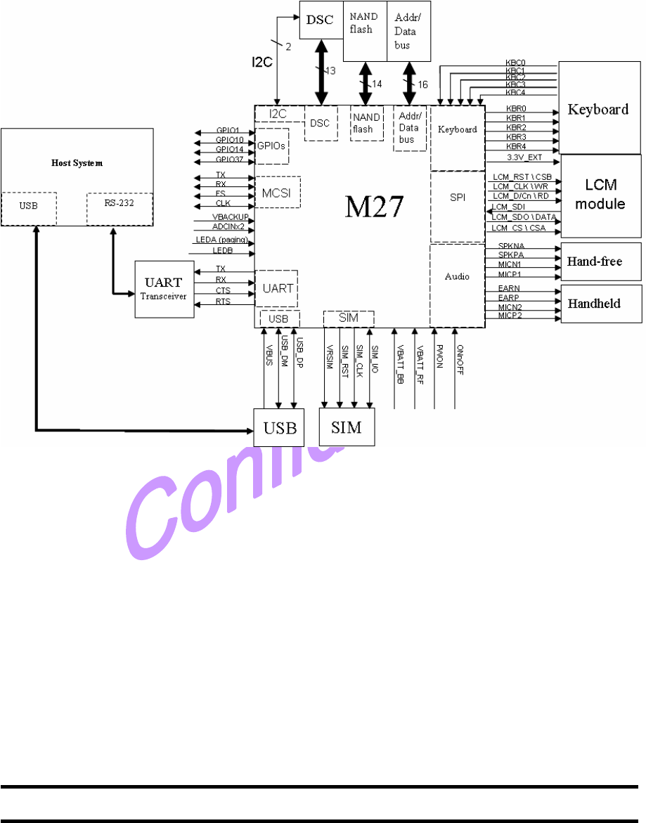
1. Overview
This design guide is based mainly on the M27 evaluation board (EVB). The M27 EVB enables you
to evaluate the M27 module and peripheral design. In addition, it provides sample firmware that you can
use as a starting point to develop code. To give the users the system concept of the interconnections
between the host and M27 module, a system block diagram is provided as the following:
The reference schematics for M27 peripherals will be given in details in this design guide. Since the
interconnections between the host and M27 vary by application, we tend to give only reference designs
of general functions, such as AT command by RS232, re-download mechanisms, and flow control of
USB, etc.

©2007 B e n Q C o r p o r a t i o n C o n f i d e n t i a l P r o p e r t y
M 27 U s e r M a n u a l V e r s i o n : 0. 1 - 2007/ J u l / 3 0
5
2. M27 Key Features at a glance
M27 provides basic features (see in the following table) for our customers, and provide compile tool
to our customers, it will gives you maximum flexibility for easy integration with the Man-Machine
Interface (MMI).
Feature Implementation
Power supply Single supply voltage 3.3V- 4.5V
Power saving Minimizes power consumption in SLEEP mode to 3mA
Charging Supports charging monitoring
Frequency bands Quad-band GSM850/EGSM900/DCS1800/PCS1900
Compliant to GSM/GPRS Phase 2/2+ , GPRS class 10
GSM class Small MS
Transmit power Class 4 (2W) at GSM850
Class 4 (2W) at EGSM900
Class 1 (1W) at DCS1800
Class 1 (1W) at PCS1900
Audio interfaces Two analog audio interfaces.
Audio features Speech codec modes:
♦ Half Rate (ETS 06.20)
♦ Full Rate (ETS 06.10)
♦ Enhanced Full Rate (ETS 06.50 / 06.60 / 06.80)
♦ Adaptive Multi Rate (AMR)
Serial interfaces: UART 1.8V Bi-directional bus for AT commands and data UART.
6-wire serial interface. Supports RTS/CTS Hardware handshake
and software XON/XOFF flow control.
Auto baud rate detects 1200 to 115200 bps
UART can be used for CSD service and send AT command of
controlling module.
UART can be multiplexing function, you can use USB at the same
time
LCM interface Support 1.8V SPI interface(CS, SDO,D/Cn, CLK, RST)
Phonebook management Supported phonebook types: SM, FD,LD, ME
SIM Application Toolkit Supports SAT class 3, GSM 11.14 Release 98
Ringing tones Offers a choice of different ringing tones / melodies, easily selectable
with AT commands
Temperature range Operational temperature : -20 ~ +к80 к
Functional temperature : -30 ~ +к85 к

©2007 B e n Q C o r p o r a t i o n C o n f i d e n t i a l P r o p e r t y
M 27 U s e r M a n u a l V e r s i o n : 0. 1 - 2007/ J u l / 3 0
6
Storage temperature : -40 ~ +85 к к
SMS MT, MO, CB, Text and PDU mode
SIM interface Supported SIM card: 1.8V/3V
External SIM card holder has to be connected via interface
connector (note that card holder is not part of M27)
External antenna Connected via 50 Ohm antenna connector or antenna pad
Real time clock Implemented
Physical characteristics Size: 45.7 x 43 x 6.8 mm
Weight: 11.0g

©2007 B e n Q C o r p o r a t i o n C o n f i d e n t i a l P r o p e r t y
M 27 U s e r M a n u a l V e r s i o n : 0. 1 - 2007/ J u l / 3 0
7
3. Design Guide Organization
The rest of the manual is organized as follows:
Section 4 Pin out definition of M27 module is given along with the RF antenna placement and
trace guidelines. In addition, the recommended power on; and handshaking
sequences are shown.
Section 5 Reference schematics for M27 peripheral, i.e., SIM, Audio, Keyboard, LCM, Paging
indicator, Camera, NAND flash, and Micro SD.
Section 6 The UART interface.
Section 7 The USB interface and USB charger solution..
Section 8 GPIO mapping.
Section 9 Level shifter design.
Section 10 Layout notice
Section 11 Antenna Interface
©2007 B e n Q C o r p o r a t i o n C o n f i d e n t i a l P r o p e r t y
M 27 U s e r M a n u a l V e r s i o n : 0. 1 - 2007/ J u l / 3 0
8
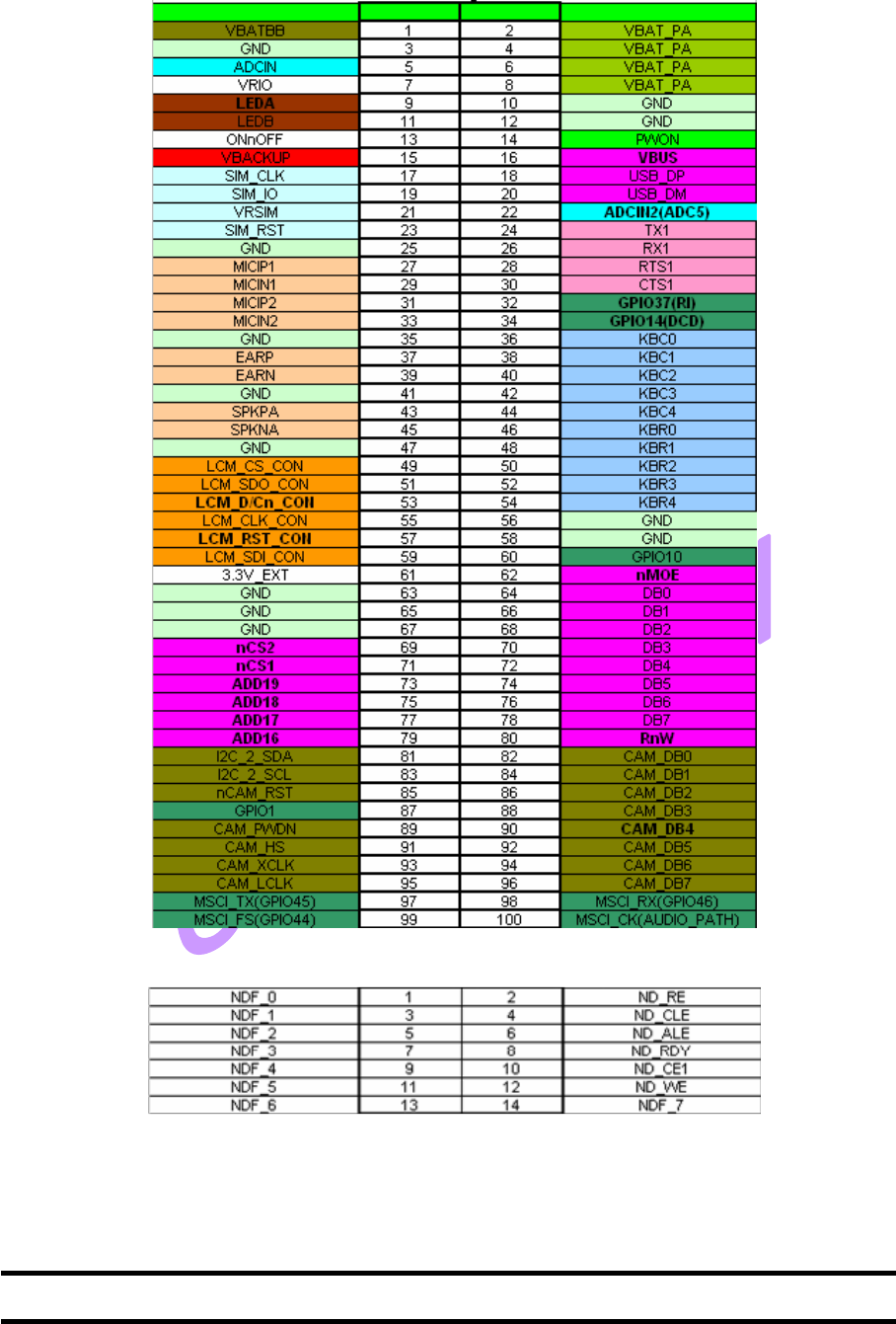
4. Pin Assignment of M27 module
The following is the pin out definition of the M27 module
NAND flash interface (14 pin assignment)
Note: For pin 97, 98, 99,100- MCSI and GPIO muxed pins, they have different functions depending on
the MODE field of the pin configuration register. Mode 0GPIO function, Mode 1MCSI function
©2007 B e n Q C o r p o r a t i o n C o n f i d e n t i a l P r o p e r t y
M 27 U s e r M a n u a l V e r s i o n : 0. 1 - 2007/ J u l / 3 0
9
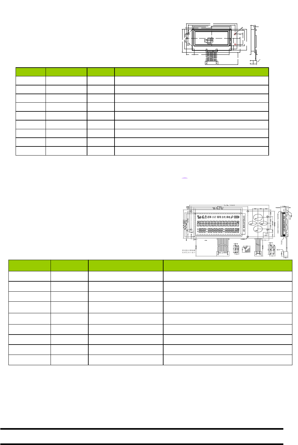
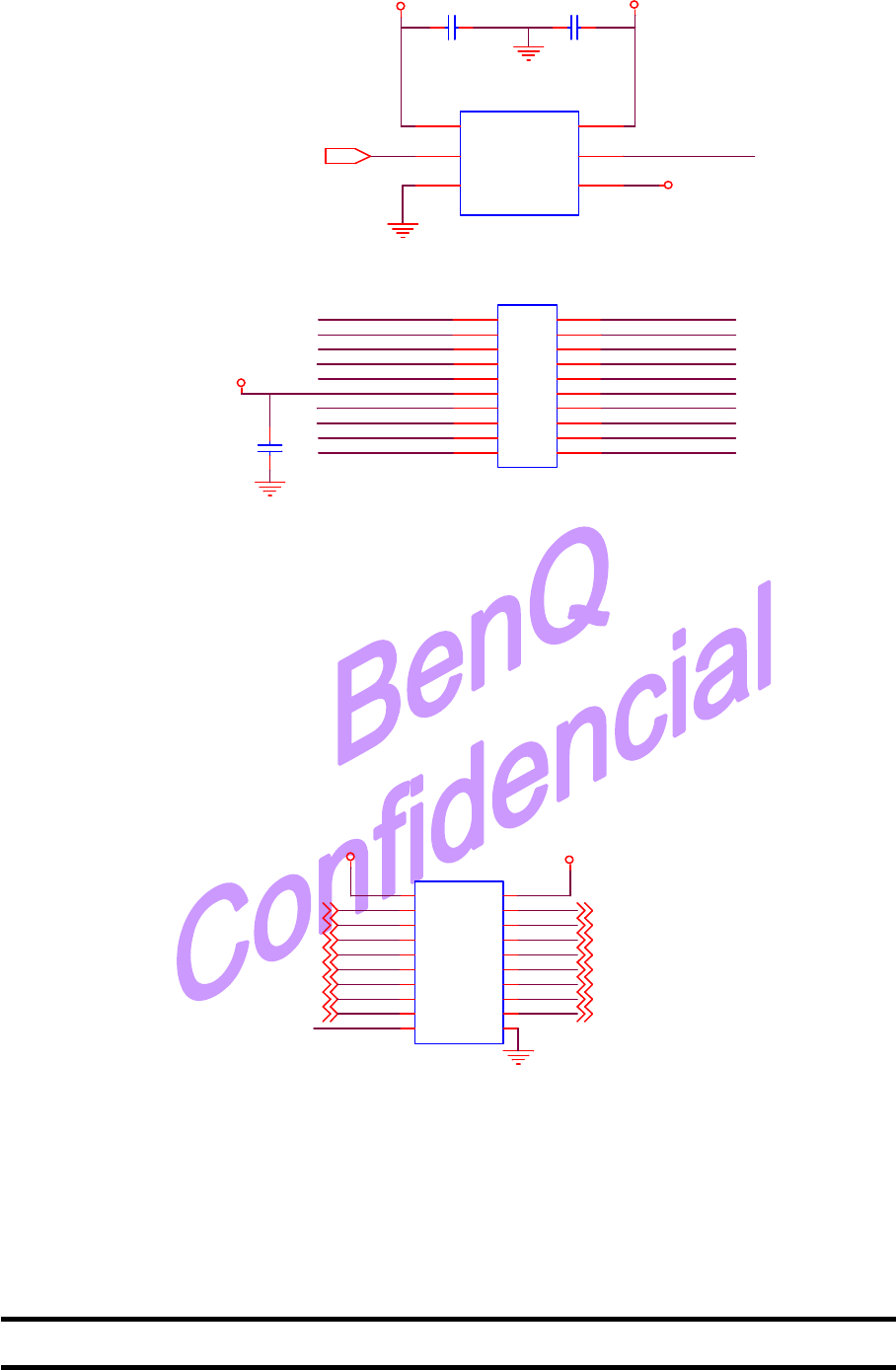
4.1. M27 Module Placement
In M27 module, we have one 50ohm antenna port (interfaced by Antenna pad and grounding) for
signal transfer. In addition, the RF signal will be impacted by high frequency noise interference. We
strongly suggest the audio trace and SIM signal trace to be as short as possible and as far away as
possible from the RF trace and power line to prevent cross coupling.
The M27 offer one approach to connecting the antenna shown in the Figure:
Antenna pad and grounding plane placed on the bottom side.
4.2. Ground Pin
There are 12 ground pins in M27 module, they should be connected to the PCB ground plane (The
ground plane in PCB should be as large as possible).
4.3. VBATRF Pin (Pin 2, Pin 4, Pin 6, Pin 8) / VBATBB Pin (Pin 1)
The “Power amplifier” is supplied by the VBATRF pins. During transmitting mode, high output
power will draw a large amount of current. The width of this power trace that is connected to the VBATRF
pins could not be less than 80mils. In addition, it is better to shunt a 100uF (low ESR) bypass capacitor
on VBATRF pins to prevent voltage drop and to reduce ripple. Furthermore, another chip in the module
is supplied by the VBATBB pin. The width of this trace that connected to this pin should also be wider.
©2007 B e n Q C o r p o r a t i o n C o n f i d e n t i a l P r o p e r t y
M 27 U s e r M a n u a l V e r s i o n : 0. 1 - 2007/ J u l / 3 0
10
4.4. PWON PIN
The pin POWON is dedicated to powering on the M27 module. The pin is initially HIGH when
power is applied to the M27 module. Once the pin is pulled low for more than 120 ms. M27 will power on.
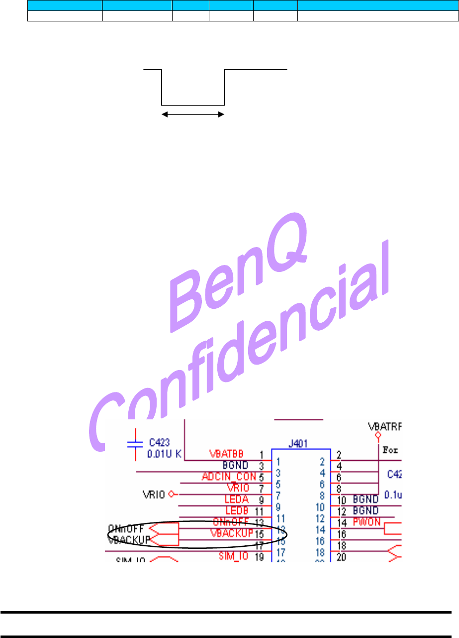
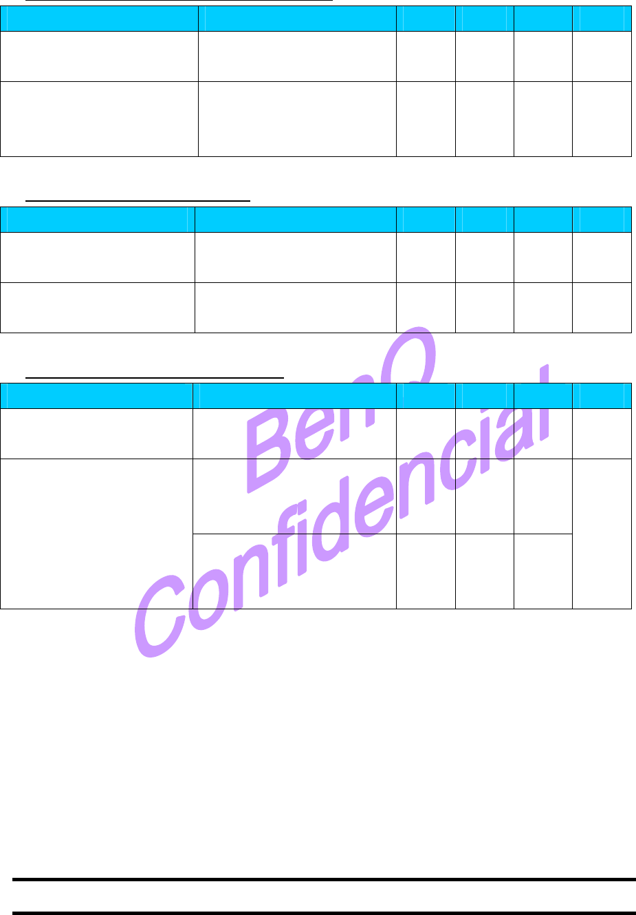
4.5. VBACKUP PIN
4.5.1 VBACKUP Main Feature
When main battery power (VBAT) is low or removed, real time information would be lost. For some
purposes, customers would like to keep some data (e.g. RTC) in above conditions that the data can be
accessed when main battery power is fed again. For example, customers need RTC continuously
running while main battery is removed. To achieve this function, M27 provides VBACKUP Pin for
backup battery connection. Backup battery would supply backup power to keep M27 RTC running.
4.5.2 Functional Description
To keep real time data for system application during low power or no power condition, M27 allows
external battery to provide power to module built-in RTC circuit via “VBACKUP” Pin. The battery can be
charged by M27 “VBACKUP” Pin as proposed in section 4.5.4. Customers could choose rechargeable
battery which meets the M27 electrical specification show in next section.
If customers would like to keep real time information alive longer than an hour, Li-ion battery would
be a better choice.
Pin Name
Pin Out
Pull
Reset
Config
Description
PWON 14 PU Input Power On
120ms
©2007 B e n Q C o r p o r a t i o n C o n f i d e n t i a l P r o p e r t y
M 27 U s e r M a n u a l V e r s i o n : 0. 1 - 2007/ J u l / 3 0
11
4.5.3Electrical Specification
Power ON / Power OFF and Backup Conditions
PARAMETER TEST CONDITIONS MIN TYP Max UNIT
Battery voltage to enter
ACTIV mode from OFF mode
Measured on the VBAT
terminal 3.3 V
Battery voltage to enter
BACKUP mode from ACTIV
mode
VBACKUP 3.2, measured on
the VBAT terminal, monitored
on the ONnOFF terminal
2.6 2.75 2.9 V
Backup Battery Charger Interface
PARAMETER TEST CONDITIONS MIN TYP Max UNIT
Backup battery charging
current
VBACKUP = 2.8 V 350 500 900 µA
End backup battery charging
voltage:
IVBACKUP = −10 µA, 2.9 3.1 3.3 V
Current consumption in BACKUP mode
PARAMETER TEST CONDITIONS MIN TYP Max UNIT
VBACKUP OFF mode VBAT=3.6V,
Ck=32KHz Clock ON 43 65 µA
VBACKUP=3.2V,
VBAT=0V,
Ck=32KHz Clock ON
8.6 12
BACKUP on backup battery
mode VBACKUP=0V,
VBAT=2.4V,
Ck=32KHz Clock ON
16 22
µA
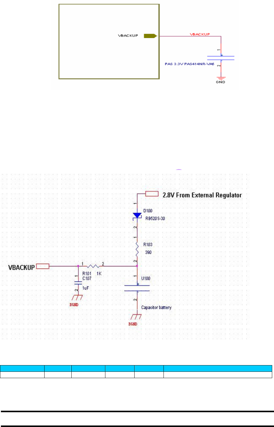
4.5.4General Charging Circuit
“VBACKUP” Pin is the in M27 to connect external Li-ion battery. This reference circuit is our
recommendation.
©2007 B e n Q C o r p o r a t i o n C o n f i d e n t i a l P r o p e r t y
M 27 U s e r M a n u a l V e r s i o n : 0. 1 - 2007/ J u l / 3 0
12
4.5.5 VBACKUP Charging
The backup battery can be charged by an external circuit or by M27 module itself via the pad
“VBACKUP”. An external circuit with a programmable voltage regulator allows recharging the backup
battery. The backup battery charge starts when the following conditions are met:
Backup battery charge is enabled by a control bit
Charging power supply (main battery) voltage > Backup Battery voltage
Charging power supply (main battery) voltage > 2.8V
4.6. ONnOFF PIN
This provide Digital Baseband Rest
Pin Name Pin Out
Pull Reset Config
Description
ON n OFF 13 PD Output Output Hardware Reset
©2007 B e n Q C o r p o r a t i o n C o n f i d e n t i a l P r o p e r t y
M 27 U s e r M a n u a l V e r s i o n : 0. 1 - 2007/ J u l / 3 0
13
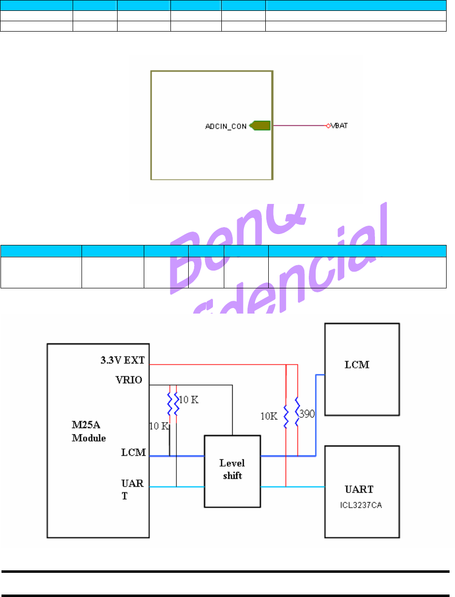
4.7. ADCIN PIN
Battery monitoring is performed by the multiplexed 10–channel 10–bit ADC MADC used to
measure the battery voltage, battery temperature, battery type, battery charge current, battery charger
input voltage and the backup battery voltage. The signals are converted into digital 10– bit words, stored
in auxiliary ADC output registers and transmitted to an external C.Γ This reference circuit is our
recommendation.
4.8. 3.3 EXT PIN
Pin Name Pin Out Pull Reset
Config
Description
3.3V_EXT 61 3.3V
Power Supply for LCM & Back light
LED
and UART in M27 EVB
Pin Name
Pin Out
Pull
Reset
Config
Description
ADCIN 5 Input Main Battery Voltage detection
ADCIN2 22 Input A/D converter

©2007 B e n Q C o r p o r a t i o n C o n f i d e n t i a l P r o p e r t y
M 27 U s e r M a n u a l V e r s i o n : 0. 1 - 2007/ J u l / 3 0
14
4.9. VRIO PIN
Power supply for external level shifters
Note: Level shifter: PMGD280UN for UART, ADG3308BRUZ-REEL for NAND flash, Add/data bus,
SN74LVCH162244AGR, PCA9306DCTR and SN74AVC1T45YZPR for Camera
Pin Name Pin Out Pull Reset
Config
Description
VRIO 7 1.8V output voltage for external
level
shifters(Note)
©2007 B e n Q C o r p o r a t i o n C o n f i d e n t i a l P r o p e r t y
M 27 U s e r M a n u a l V e r s i o n : 0. 1 - 2007/ J u l / 3 0
15
5 Peripherals
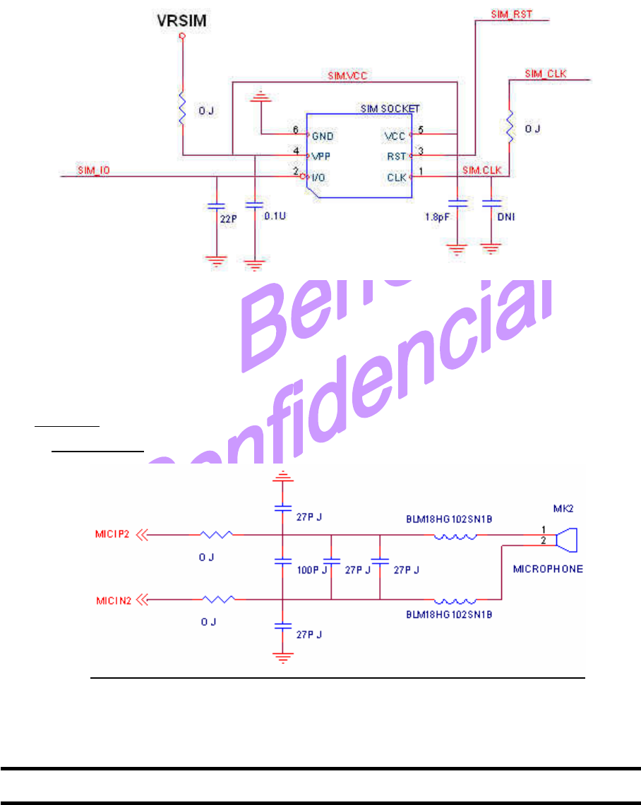
5.1. SIM
The SIM Card digital interface in the M27 ensures the translation of logic levels between M27 and the
SIM Card, for the transmission of 3 different signals: SIM_CLK; a reset signal from M27 to the SIM
Card (SIM_RST); and serial data from M27 to the SIM Card (SIM_IO). The SIM card interface can be
programmed to drive a 1.8V SIM Card.
6 Pin SIM Socket
5.2. Audio
There are 2 embedded audio drivers built in the BenQ M27 module. The 2 drivers can drive different
kinds of audio load (such as Handheld, or hands free).
Handheld
Microphone 2
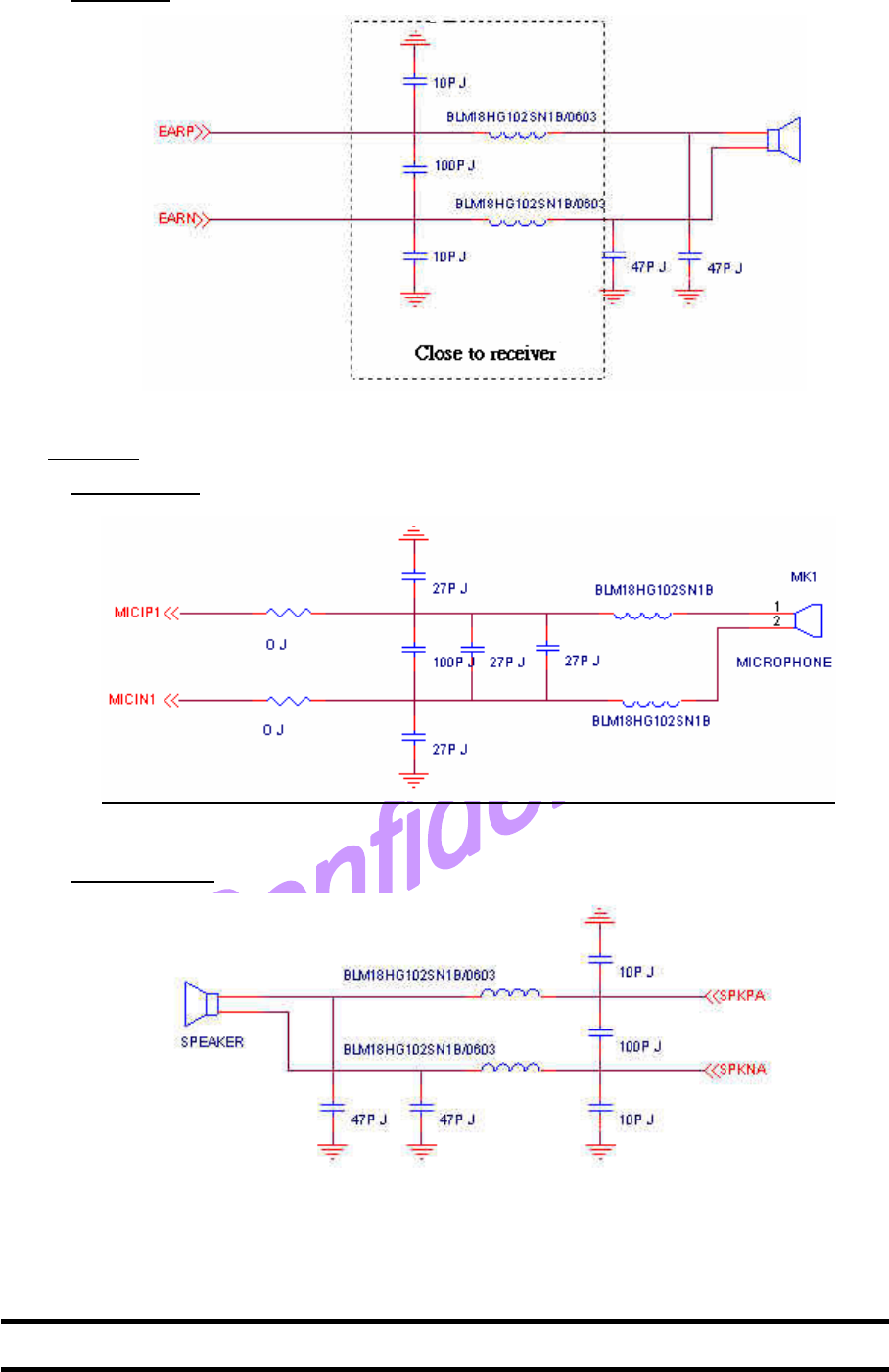
©2007 B e n Q C o r p o r a t i o n C o n f i d e n t i a l P r o p e r t y
M 27 U s e r M a n u a l V e r s i o n : 0. 1 - 2007/ J u l / 3 0
16
Ear output
Hand free
Microphone 1
Speaker output
©2007 B e n Q C o r p o r a t i o n C o n f i d e n t i a l P r o p e r t y
M 27 U s e r M a n u a l V e r s i o n : 0. 1 - 2007/ J u l / 3 0
17
Audio Path Selection AT Commands
The M27 module provides the switching of audio paths using AT commands (In connection status):
Default value: case (1)
(1) AT$HANDHELD (EARN, EARP, MICIN2, MICIP2)
(2) AT$HANDFREE (SPKPA, SPKNA, MICIN1, MICIP1)
5.3. KEYBOARD
5.3.1 Keyboard Controller Overview
The keyboard controller can handle up to 5*5 keyboards, operates on a 32-kHz clock, and can
generate wake-up events when the device is in sleep mode, and this reference circuit is our
recommendation.
Pin Name Pin Out
Pull Reset Config
Description
KBR0 46 PU Input high Keypad matrix 4 Row access
KBR1 48 PU Input high Keypad matrix 4 Row access
KBR2 50 PU Input high Keypad matrix 4 Row access
KBR3 52 PU Input high Keypad matrix 4 Row access
KBR4 54 PU Input high Keypad matrix 4 Row access
KBC0 36 Output Keypad matrix 4 column access
KBC1 38 Output Keypad matrix 4 column access
KBC2 40 Output Keypad matrix 4 column access
KBC3 44 Output Keypad matrix 4 column access
KBC4 46 Output Keypad matrix 4 column access
5.3.2 Reference circuit
5.3.3 Main Features
ROW4
C37 22P J
C38 22P J
C39 22P J
C40 22P J
C41 22P J
ROW0
ROW2
ROW4 ROW3
ROW1
T3 15V 150PF
.
1.2
T2 15V 150PF
.
1.2
T4 15V 150PF
.
1.2
T5 15V 150PF
.
1.2
T6 15V 150PF
.
1.2
KBC0
KBC2
KBC4
KBC1
KBC3
KBR0
KBC0
Close to the Key Pad
connector
KBC2KBC1
KBC3 KBC4
J8
KB connector
1
122
3
344
5
566
7
788
9
910 10
ROW4
ROW2
ROW0
KBC1
ROW3
KBC0
ROW1
KBC2
KBC3 KBC4
R31
100 J
R32
100 J
R33
100 J
R34
100 J
R35
100 J
KBR1
KBR3
KBR2
KBR4
ROW0
ROW1
ROW2
ROW3
©2007 B e n Q C o r p o r a t i o n C o n f i d e n t i a l P r o p e r t y
M 27 U s e r M a n u a l V e r s i o n : 0. 1 - 2007/ J u l / 3 0
18
The keyboard controller includes the following main features:
- Support of multi-configuration keyboards up to 5 rows x 5 columns
- Integrated programmable timer
- Programmable interrupt (IT) generation on key events
- Event detection on both key press and key release
- Multi-key press detection and decoding
- Long key detection on prolonged key press
- Programmable time-out on permanent key press or after keyboard release
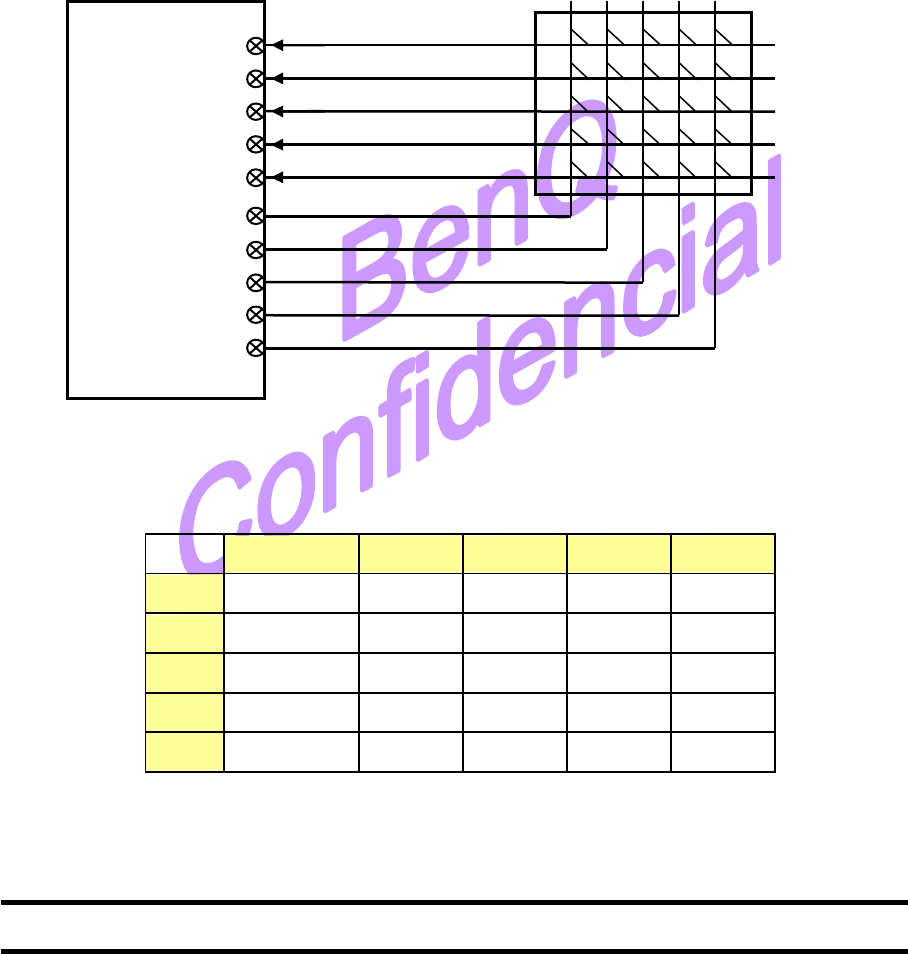
5.3.4 Signals and I/O Description
Figure shows a typical 5*5 keyboard connection to the M27 keyboard controller.
5.3.5 Key Mapping
C0 C1 C2 C3 C4
R0 Select Up Down Dial Return
R1 Vol+ 1 2 3 SMS
R2 Vol- 4 5 6 ESC
R3 Re-Dial 7 8 9 Del
R4 Handfree * 0 # Set
Matrix Keyboard
M27
Module
KBR0
KBR1
KBR2
KBR3
KBR4
KBC0
KBC1
KBC2
KBC3
KBC4
©2007 B e n Q C o r p o r a t i o n C o n f i d e n t i a l P r o p e r t y
M 27 U s e r M a n u a l V e r s i o n : 0. 1 - 2007/ J u l / 3 0
19
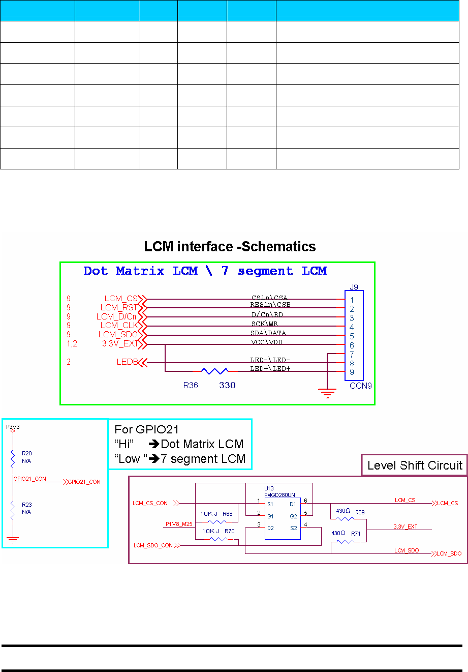
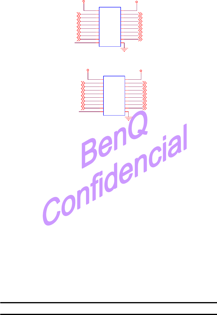
5.4. LCM (SPI interface)
M27 Provides SPI LCM interface for customer application, it gives you the flexibility to develop
customized application, and this reference circuit is our recommendation.
Pin Name Pin Out Pull Reset Config
Description
3.3_EXT 61
Power Supply for LCM & Back light LED
LCM_CS 49 Chip Select \ Chip Select A
LCM_SDO 51 Serial input data \ Serial Input Data
LCM_D/Cn 53 Register select Input pin
(Data/Instruction) \ Read signal
LCM_CLK 55 Serial Input clock \ Write signal
LCM_RST 57 Reset Input Pin \ Chip Select B
LEDB 11 Back light LED Sink
5.4.1 Reference schematics
5.4.2 Dot Matrix LCM spec
©2007 B e n Q C o r p o r a t i o n C o n f i d e n t i a l P r o p e r t y
M 27 U s e r M a n u a l V e r s i o n : 0. 1 - 2007/ J u l / 3 0
20
Dot Matrix LCM spec
SHENZHEN WELLST WGM12864COG-21
General specifications
Display format: 128 * 64 dot matrix graphic
Microprocessor interface: Serial
Power level: 3.3V
Module size: 92 x 57X8 mm
Definition of Terminals
Power supply for LED3VLED+9
Power supply for LED0VLED-8
Ground0VGND7
Power supply for lcm3.0VVCC6
Serial input dataH/LSDA5
Serial input clockH/LSCK4
Register select input pin (Data/Instruction )H/LD/C3
Reset input pin LRES1B2
Chip selectLCS1B1
FunctionLevelSymbolPin No.
0. 4 5
0. 47 5
0.49
0.5 1 5
DOTS: 1 2 8 *6 4
6 5 . 5V . A
3 8 .0V .A
5 2 .0± 0. 2
1 . 6
MAX 8.0
MAX 12.0
7 1 . 1
1 9. 0
3 0. 0
8 . 0
2 0. 0
48 . 3
9 2 . 0
8 6 . 0
5 7 .0
1 0.5
2 6 .0
43 . 03 . 0
3 5 .0
1 1 .5
6 4 . 01 4 . 0
1
130
9
2 . 5 4 X 7 = 2 0 . 3 2
19
6 . 0
8 . 0
է ڬ
5.4.2 7 Segment LCM spec
7 segment LCM spec
څતᔲຏ ˪ ˦ ˠ ˀˉ ˋ ˉ ˄ ˔
General specifications
Definition of Terminals
Display format: 29 Digit(7 segment)+24 Prompt
Microprocessor interface: Serial
Power level: 3.3V
Module size: 115.5 x 48X12 mm
sink pin for LED0VLED-9
Power supply for LED3.3VLED+8
Chip Select BCMOS (In) (Pull up)/CSB7
Chip Select ACMOS (In) (Pull up)/CSA6
Read signal (Rising edge trigger)CMOS (In) (Pull up)/RD5
Write signal (Rising edge trigger)CMOS (In) (Pull up)/WR4
Serial input dataCMOS (In) (Pull up)DATA3
Ground0VGND2
Main Power3.3VVDD1
FunctionLevelSymbolPin No.
©2007 B e n Q C o r p o r a t i o n C o n f i d e n t i a l P r o p e r t y
M 27 U s e r M a n u a l V e r s i o n : 0. 1 - 2007/ J u l / 3 0
21
5.5. LCM (parallel bus interface)
M27 provides parallel bus (8 bit) LCM interfaces for customer application. It gives you the
flexibility to develop customized application, and a reference circuit is provided here.
LCM parallel bus signal pins of M27 module
Pin Name Pin Out Pull Reset Config
Description
DATA/ADD0 64 Bit 0 for Data bus
DATA/ADD1 66 Bit 1 for Data bus
DATA/ADD2 68 Bit 2 for Data bus
DATA/ADD3 70 Bit 3 for Data bus
DATA/ADD4 72 Bit 4 for Data bus
DATA/ADD5 74 Bit 5 for Data bus
DATA/ADD6 76 Bit 6 for Data bus
DATA/ADD7 78 Bit 7 for Data bus
RnW 80 Write signal
nMOE 62 Read signal
GPIO37 32 A0==>Command/Data
GPIO14 34 Reset
3.3V_EXT 61 3.3V power supply
5.5.1 Reference schematics (LCM connector pins on M27 EVB)
P18V
VBAT
X1
X2 Y1
Y2
GND
VBAT
GPIO14
Reset
C150
0.1U K
GND
A0==>Command/Data
P18V
DATA_ADD6_PAD
3.3V_EXT
J404
LCD 8bit connector
1
1
10 10
3
3
12 12
5
5
14 14
7
7
16 16
9
9
19
19 17
17 15
15
11
11
13
13
18 18
20 20
22 22
24 24
23
23 21
21
88
66
44
22
DATA_ADD4_PAD
DATA_ADD0_PAD
RnW_PAD
DATA_ADD2_PAD
DATA_ADD5_PAD
GND
DATA_ADD7_PAD
DATA_ADD3_PAD
nCS1_PAD
GPIO37
nMOE_PAD
DATA_ADD1_PAD
©2007 B e n Q C o r p o r a t i o n C o n f i d e n t i a l P r o p e r t y
M 27 U s e r M a n u a l V e r s i o n : 0. 1 - 2007/ J u l / 3 0
22
Level shifters between M27 pins and LCM connector
3.3V_EXT
P1V8_M27
U4
ADG3308BRUZ-REEL
VCCA
1
A2
3
A4
5A3
4
A1
2
A5
6
A6
7
A7
8
A8
9
EN
10 GND 11
VCCY 20
Y1 19
Y2 18
Y3 17
Y4 16
Y5 15
Y6 14
Y7 13
Y8 12
3.3V_EXT
GND
DATA_ADD73 DATA_ADD63 DATA_ADD53 DATA_ADD43 DATA_ADD33 DATA_ADD23 DATA_ADD13 DATA_ADD03
DATA_ADD7_PAD
DATA_ADD6_PAD
DATA_ADD5_PAD
DATA_ADD4_PAD
DATA_ADD3_PAD
DATA_ADD2_PAD
DATA_ADD1_PAD
DATA_ADD0_PAD
RnW_PAD
ADD16_PAD
ADD17_PAD
ADD18_PAD
ADD19_PAD
nCS1_PAD
nCS2_PAD
nMOE_PAD
RnW3 ADD163 ADD173 ADD183 ADD193 nCS13 nCS23 nMOE3
U3
ADG3308BRUZ-REEL
VCCA
1
A2
3
A4
5A3
4
A1
2
A5
6
A6
7
A7
8
A8
9
EN
10 GND 11
VCCY 20
Y1 19
Y2 18
Y3 17
Y4 16
Y5 15
Y6 14
Y7 13
Y8 12
3.3V_EXT
P1V8_M27
3.3V_EXT
GND
©2007 B e n Q C o r p o r a t i o n C o n f i d e n t i a l P r o p e r t y
M 27 U s e r M a n u a l V e r s i o n : 0. 1 - 2007/ J u l / 3 0
23
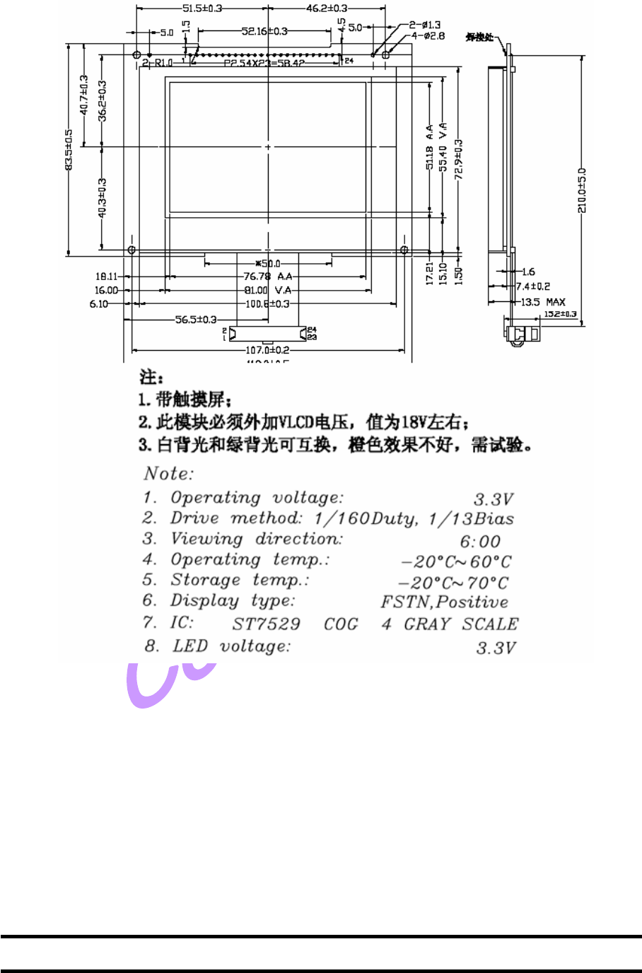
5.5.2 Dimension and Pin assignment for parallel bus type LCM (YMC240160-04AAAYDGL)
©2007 B e n Q C o r p o r a t i o n C o n f i d e n t i a l P r o p e r t y
M 27 U s e r M a n u a l V e r s i o n : 0. 1 - 2007/ J u l / 3 0
24
Pin assignment of parallel bus type LCM (YMC240160-04AAAYDGL)
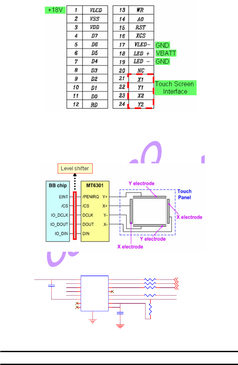
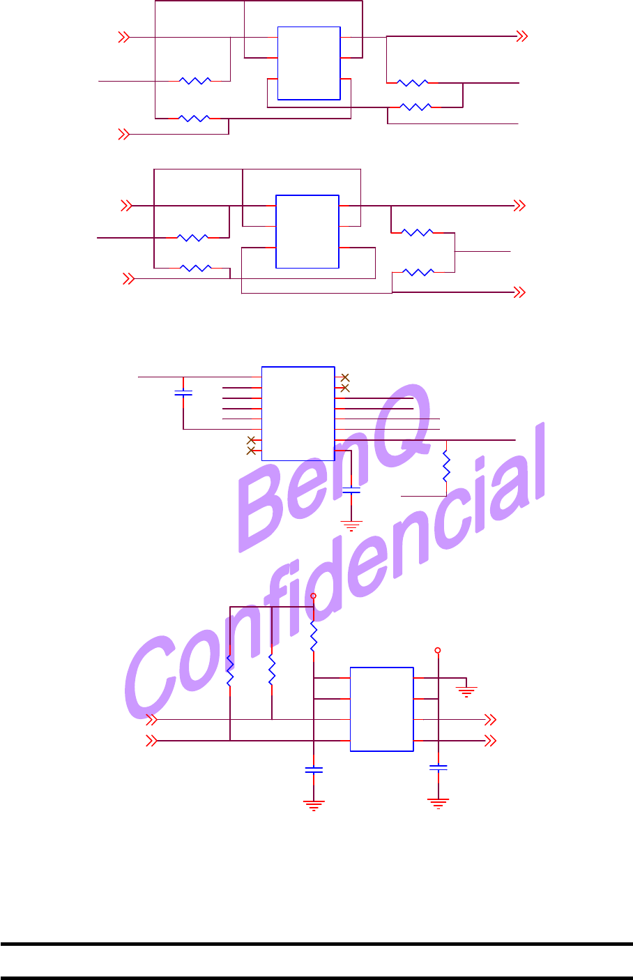
5.6. Touch screen controller
For USB charger application, there are two choices for the touch screen controller with SPI
interface or I2C interface.
5.6.1 SPI type touch screen controller(MTK MT6301)
3.3V_EXT C146
0.1U K
LCM_CS 5
LCM_CLK 5
LCM_SDO 5
R167
0 0402
R168
0 0402
R169
0 0402
R171
0 0402
LCM_SDI
GND
R173
47K J
3.3V_EXT
GND
C147
0.1U K
X1
U25
MT6301
+Vcc
5
Y+
7
Y-
9X-
8
X+
6
GND
10
VBAT
11
AUX
12 Vref 13
IOVdd 14
PenIRQ 15
Dout 16
Busy 1
Din 2
nCS 3
DCLK 4
GND
17
Y1
X2
Y2 PenIRQGND
©2007 B e n Q C o r p o r a t i o n C o n f i d e n t i a l P r o p e r t y
M 27 U s e r M a n u a l V e r s i o n : 0. 1 - 2007/ J u l / 3 0
25
LCM_SDI_CON3
LCM_SDI
LCM_CLK 5
U15
PMGD280UN
S1
1
D2
3
G2 5
S2 4
G1
2
D1 6
3.3V_EXT
LCM_CLK
R76
10K J
R77
10K J
LCM_CLK_CON3
P1V8_M27
R78
10K J
R79
10K J
LCM_CS_CON3 LCM_CS 5
LCM_SDO_CON3
LCM_SDO 5
U13
PMGD280UN
S1
1
D2
3
G2 5
S2 4
G1
2
D1 6
LCM_SDO
3.3V_EXT
LCM_CS
P1V8_M27 R68
10K J
R69
10K J
R70
10K J
R71
10K J
5.6.2 I
2
C type touch screen controller(TI TSC2003)
U28 TSC2003
+Vdd
1
Y+
3
Y-
5X-
4
X+
2
GND
6
Vbat1
7
Vbat2
8Vref 9
PENIRQ 10
SDA 11
SCL 12
A1 13
A0 14
IN2 15
IN1 16
X1
Y1
Y2
X2
3.3V_EXT C149
0.1U K
GND
R172
47K J
PenIRQ
3.3V_EXT
GND
GND
I2C_SCL_PAD
I2C_SDA_PAD
C148
0.1U K
GND
C144
0.1U K
C145
0.1U K
GND
GND
P1V8_M27
GND
R164
150K
3.3V_EXT
R165
10K J
R166
10K J
U22
PCA9306DCTR
GND 1
SCL1 3
SDA2
5SDA1 4
Vref1 2
SCL2
6
Vref 2
7
EN
8
I2C_SCL 3
I2C_SDA 3
I2C_SCL_PAD
I2C_SDA_PAD
©2007 B e n Q C o r p o r a t i o n C o n f i d e n t i a l P r o p e r t y
M 27 U s e r M a n u a l V e r s i o n : 0. 1 - 2007/ J u l / 3 0
26
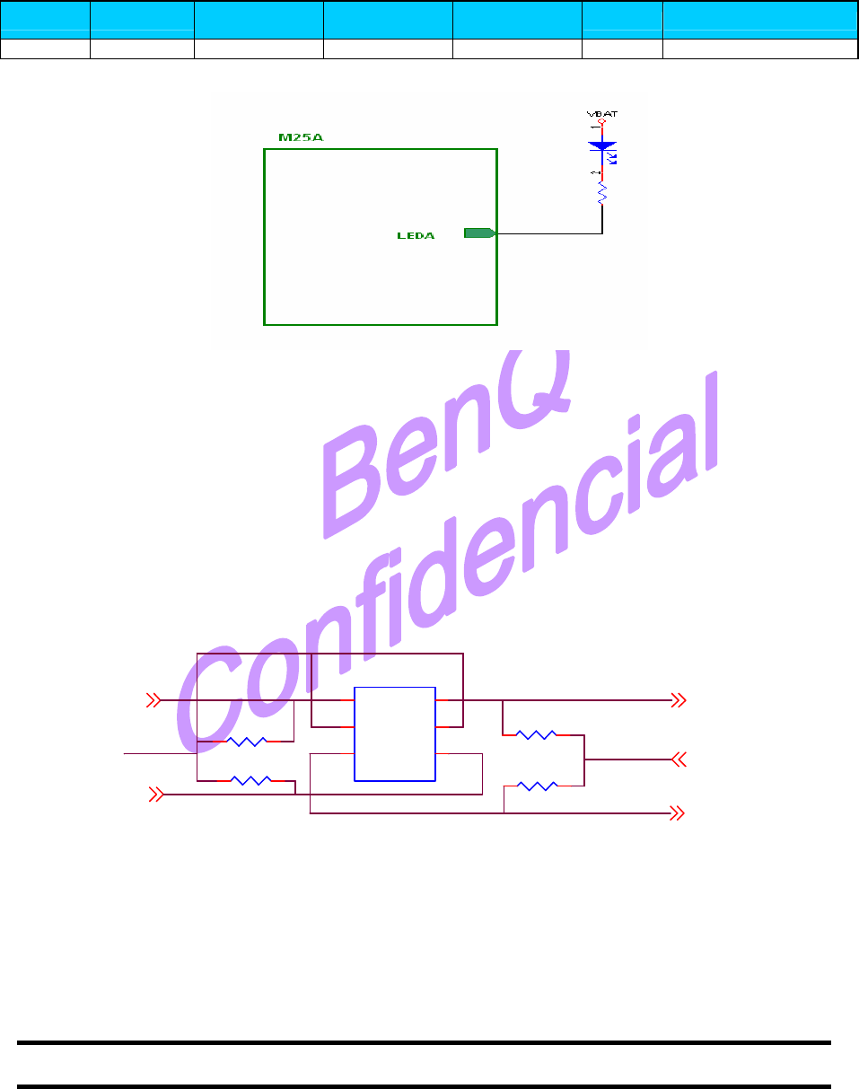
5.7. Paging Indicator
LEDA is dedicated for paging indication. The application circuit is shows as below. The diagram
below illustrates the application schematic for LED driver inputs LEDA. In each case the current
limiter resistor R has to be selected in order to be compliant with maximum current drive capability of
each input.
Name Pin Max drive
current
Highest level
voltage
Lowest level
voltage supply
Description
LEDA 9 20mA VBATBB 2.4 VBATBB
paging indicator
LEDA is controlled through software program using a dedicated GPIO, which is built in the M27
module, it can write program to control the LED pin state.
5.8. Camera interface
The camera interface supports data in ITU-R BT.656 format. The ITU-R BT.656 Standard specifies
a method for transferring YUV422 data over an 8-bit interface. The Parallel Camera module can provide
a Camera Reference clock (CAM_XCLK) to the camera sensor based on on-chip APLL (48MHz) clock
sources
CAM_PWDN_PAD
nCAM_RST_PAD
3.3V_EXT
CAM_PWDN3
nCAM_RST3
P1V8_M27
U20
PMGD280UN
S1
1
D2
3
G2 5
S2 4
G1
2
D1 6
3.3V_EXT 3,5,7,8
R162
10K J
R160
10K J
R161
10K J
R163
10K J
560Ө
©2007 B e n Q C o r p o r a t i o n C o n f i d e n t i a l P r o p e r t y
M 27 U s e r M a n u a l V e r s i o n : 0. 1 - 2007/ J u l / 3 0
27
C144
0.1U K
C145
0.1U K
GND
GND
P1V8_M27
GND
R164
150K
3.3V_EXT
R165
10K J
R166
10K J
U22
PCA9306DCTR
GND 1
SCL1 3
SDA2
5SDA1 4
Vref1 2
SCL2
6
Vref 2
7
EN
8
I2C_SCL 3
I2C_SDA 3
I2C_SCL_PAD
I2C_SDA_PAD
CAM_DB4_PAD
CAM_DB3_PAD
CAM_DB2_PAD
CAM_DB1_PAD
CAM_DB0_PAD
CAM_PWDN_PAD
C140
0.1U K
C141
0.1U K
C142
0.1U K
C143
0.1U K
GND
U21
SN74LVCH162244AGR
Gnd1
4
Gnd2
10
Gnd3
15
Gnd4
21
Gnd5
28
Gnd6
34
Gnd7
39
Gnd8
45
Vcc1 7
Vcc2 18
Vcc3 31
Vcc4 42
1Y0 2
1Y1 3
1Y2 5
1Y3 6
2Y0 8
2Y1 9
2Y2 11
2Y3 12
3Y0 13
3Y1 14
3Y2 16
3Y3 17
4Y0 19
4Y1 20
4Y2 22
4Y3 23
1A0
47
1A1
46
1A2
44
1A3
43
1OE
1
2A0
41
2A1
40
2A2
38
2A3
37
2OE
48
3A0
36
3A1
35
3A2
33
3A3
32
3OE
25
4A0
30
4A1
29
4A2
27
4A3
26
4OE
24
GND
GND
CAM_DB0 3
CAM_DB1 3
CAM_DB3_CAM_VS 3
CAM_DB2 3
CAM_DB5 3
CAM_DB4 3
CAM_DB7 3
CAM_DB6 3
CAM_HS 3
CAM_LCLK 3
P1V8_M27
CAM_HS_PAD
CAM_LCLK_PAD
CAM_DB7_PAD
CAM_DB6_PAD
CAM_DB5_PAD
©2007 B e n Q C o r p o r a t i o n C o n f i d e n t i a l P r o p e r t y
M 27 U s e r M a n u a l V e r s i o n : 0. 1 - 2007/ J u l / 3 0
28
C70
0.1U K
C71
0.1U K
P1V8_M27
CAM_XCLK3 CAM_XCLK_PAD
P1V8_M27 3.3V_EXT
U27
SN74AVC1T45YZPR
A
3
GND
2
VCCA
1VCCB 6
B4
DIR 5
GND
GND
CAM_DB7_PAD
CAM_DB0_PAD
CAM_DB1_PAD
CAM_DB2_PAD
CAM_DB3_PAD
GND
CAM_HS_PAD
J403
DSC connector
1
120 20
2
219 19
3
318 18
4
417 17
5
5
10
10 9
98
8
6
6
7
7
16 16
15 15
14 14
13 13
12 12
11 11
CAM_PWDN_PAD
CAM_LCLK_PAD
GND
P2V5
C159
0.1U K
I2C_SDA_PAD
CAM_XCLK_PAD
I2C_SCL_PAD
nCAM_RST_PAD
CAM_DB6_PAD
CAM_DB5_PAD
CAM_DB4_PAD
GND
CAM_VSYNC
P1V8_M27
5.9. NAND flash interface
The aim of this NAND flash controller is to have a fully automatic transfer process from/to
the NAND flash port. The interface implements an 8-bit parallel data bus (commands, addresses, and
data are multiplexed) in addition to the control signals for selecting chip, writing/reading, command and
address latching, and ready/busy status. The NAND flash chip used in M27 EVB is Samsung
K9F5608U0D-JIB0 FBGA (
32M x 8 Bit Memory
).It is necessary to add 2 pcs of bi-directional level
shifter to interface the M27 and the NAND flash chip.
NDF_2 3
NDF_1 3
NDF_0 3
NDF_5 3
NDF_4 3
NDF_3 3
NDF_7 3
NDF_6 3
NDF_1_M253 NDF_0_M253
NDF_2_M253
NDF_4_M253 NDF_3_M253
NDF_6_M253 NDF_5_M253
NDF_7_M253
U31
ADG3308BRUZ-REEL
VCCA
1
A2
3
A4
5A3
4
A1
2
A5
6
A6
7
A7
8
A8
9
EN
10 GND 11
VCCY 20
Y1 19
Y2 18
Y3 17
Y4 16
Y5 15
Y6 14
Y7 13
Y8 12
P1V8_M27 3.3V_EXT
GND
3.3V_EXT
©2007 B e n Q C o r p o r a t i o n C o n f i d e n t i a l P r o p e r t y
M 27 U s e r M a n u a l V e r s i o n : 0. 1 - 2007/ J u l / 3 0
29
ND_ALE 3
ND_CLE 3
ND_RE 3
ND_CE1 3
ND_RDY 3
ND_WE 3
ND_CLE_M253 ND_RE_M253
ND_CE1_M253
ND_RDY_M253 ND_ALE_M253
ND_WE_M253
P1V8_M27 3.3V_EXT
U32
ADG3308BRUZ-REEL
VCCA
1
A2
3
A4
5A3
4
A1
2
A5
6
A6
7
A7
8
A8
9
EN
10 GND 11
VCCY 20
Y1 19
Y2 18
Y3 17
Y4 16
Y5 15
Y6 14
Y7 13
Y8 12
GND
3.3V_EXT
U2
K9F5608U0D-JIB0
IO0 F2
IO1 G2
IO2 H2
IO3 H3
IO4 H4
IO5 G5
IO6 H5
IO7 G6
/CE
A4
/RE
B2
/WE
A5
ALE
A2
CLE
B3
VCC F6
VSS
A3
VSS
H1
/WP
A1
R/B
A6
LOCKPRE E6
VCCQ G4
VSS
H6
3.3V_EXT
NDF_2
NDF_4
NDF_0
NDF_3
NAND_PRE
NDF_7
NDF_5
NDF_6
ND_CE1
ND_RE
ND_CLE
NDF_1ND_RDY
ND_WE
ND_ALE
32MX8bit, 1.8V interface
3.3V_EXT
R704
0 0402
NDF_0 9
NDF_4 9
NDF_3 9
NDF_2 9
NDF_1 9
NDF_7 9
NDF_5 9
NDF_6 9
ND_RE9
ND_CLE9
ND_RDY9
ND_ALE9 ND_WE9
ND_CE19
©2007 B e n Q C o r p o r a t i o n C o n f i d e n t i a l P r o p e r t y
M 27 U s e r M a n u a l V e r s i o n : 0. 1 - 2007/ J u l / 3 0
30
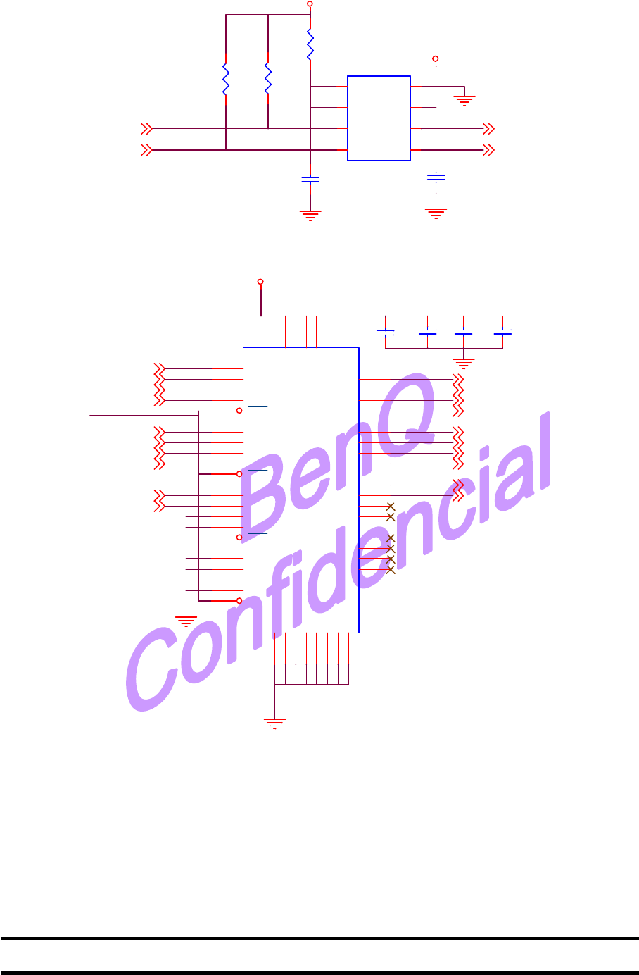
5.10. Micro SD interface
The micro-SD card SPI interface is compatible with SPI hosts available on the market. As any other
SPI device the micro-SD card SPI channel consists of the following 4 signals: CS, CLK, DI, DO
U9
SN74LVC2T45DCUR
A1
2
A2
3
GND
4
VCCA
1VCCB 8
B2 6
B1 7
DIR 5
U8
SN74LVC2T45DCUR
A1
2
A2
3
GND
4
VCCA
1VCCB 8
B2 6
B1 7
DIR 5
J1
GND
1
CS
2DI/CMD
3
VDD
4
CLK
5
VSS
6
DO/DATA
7
GND
8
GND
9
GND
10
CARD DETECT
12
R22
DNI_10K
12
1.8V
P1V8
1.8V
3.3V
3.3V
CARD DETECT
DATA
CS
C10
0.1U K
C11
0.1U K
C12
0.1U K
C13
0.1U K
VRIO
CLK
BGND
C8
0.1uF
C9
0.1uF
3.3V
BGND
1.8V
U7
SN74AVC1T45YZPR
A
3
GND
2
VCCA
1VCCB 6
B4
DIR 5
CLK
DATA
CARD DETECT
CS
CMD CMD
3.3V
Trans Flash card connector
©2007 B e n Q C o r p o r a t i o n C o n f i d e n t i a l P r o p e r t y
M 27 U s e r M a n u a l V e r s i o n : 0. 1 - 2007/ J u l / 3 0
31
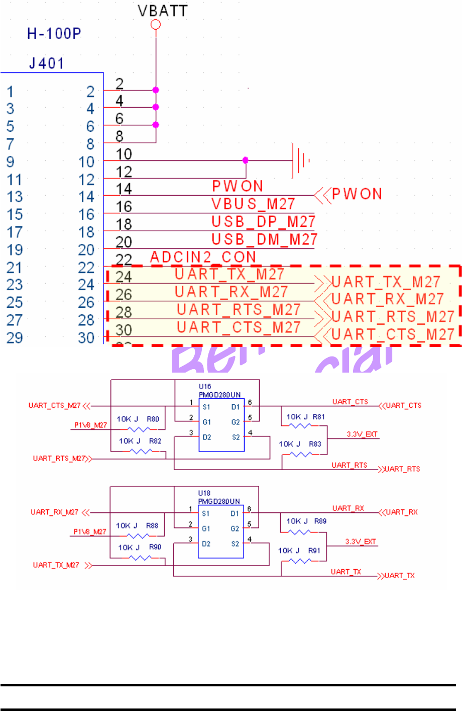
6 UART Interface
UART/RS232
The UART includes the following additional features
- Hardware flow control (such as RTS/CTS) consists of two control signal lines between the Host
(DTE) and Client (DCE) that are used to control the flow of data between the devices.
- Auto-baud rate with the possibility of baud-rates ranging from 1200 to 115.2K bits.
Pin Name
Pin Out Pull Reset Config
Description
TX 24 Output / 1
UART-Transmit Data(M27 side)
RX 26 PU Input UART-Receive Data(M27 side)
RTS 28 1 UART-Request To Send(M27 side)
CTS 30 PD Input UART-Clear To Send(M27 side)
Note: The difference between Reset and Config in the pin definition table
M27 only provide 1.8V UART interface. If the host (DTE) is 3.3V system, it needs additional Level
shifter circuit on EVB.
UART Interfaces
ٛTX
RX
RTS
CTS
DCD
RI
GND
DSR
DTR
RX
TX
CTS
RTS
DCD
RI
GND
Client Device
M27 (DCE)
HOST Device
(DTE)
VDD2=3.3V
VDD1=1.8V
Level shift
10K 10K
©2007 B e n Q C o r p o r a t i o n C o n f i d e n t i a l P r o p e r t y
M 27 U s e r M a n u a l V e r s i o n : 0. 1 - 2007/ J u l / 3 0
32
UART interface on M27
1.8V-3.3V level shifter for UART interface
©2007 B e n Q C o r p o r a t i o n C o n f i d e n t i a l P r o p e r t y
M 27 U s e r M a n u a l V e r s i o n : 0. 1 - 2007/ J u l / 3 0
33
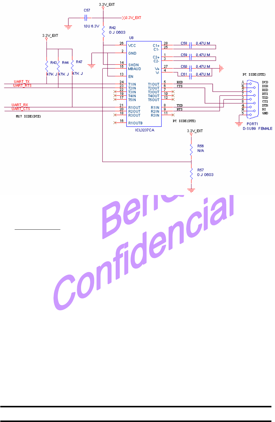
UART transceiver ICL3237A
HW flow control
When the hardware flow control type is recommended for communication between the Host(DTE)
and client(DCE). Regarding the hardware flow control mechanism between the system (host side) and
module (client side).
The GSM engine is designed for use as a DCE. Based on the conventions for DCE-DTE Connections it
communicates with the customer application (DTE) using the following signals:
♦ Port/TX @ Host Device sends data to the module’s /RX signal line
♦ Port/RX @ Host Device receives data from the module’s /TX signal line
♦ Port/RTS @ Host Device sends data to the module’s /CTS signal line
♦ Port/CTS @ Host Device receives data from the module’s /RTS signal line

©2007 B e n Q C o r p o r a t i o n C o n f i d e n t i a l P r o p e r t y
M 27 U s e r M a n u a l V e r s i o n : 0. 1 - 2007/ J u l / 3 0
34
Auto baud Rate Mechanism
The M27 module UART is set at Auto-baud rate. This means when the M27 is powered on, it
automatically detects the baud rate after the first AT command sent by the host Device. The baud rate is
locked at the initially detected rate unless the following conditions:
Client
Device
HOST
Device
TX
RX
RTS
CTS
DCD
RI
GND
DSR
DTR
TX
RX
RTS
CTS
DCD
RI
GND
©2007 B e n Q C o r p o r a t i o n C o n f i d e n t i a l P r o p e r t y
M 27 U s e r M a n u a l V e r s i o n : 0. 1 - 2007/ J u l / 3 0
35
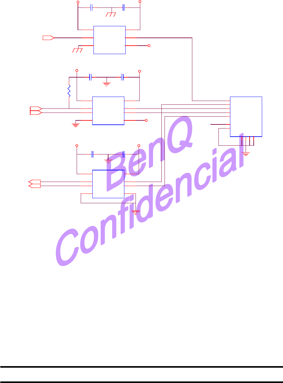
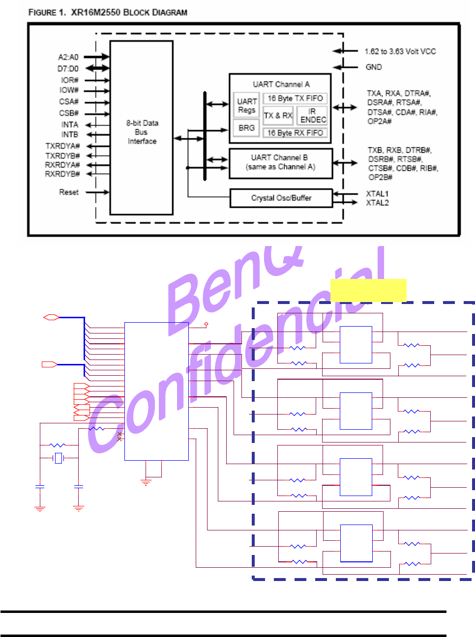
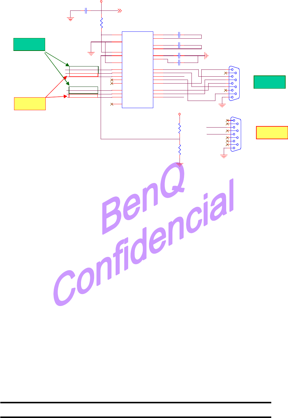
6.1 Dual external UART solution
M27 support 1 UART interface. M27 module support 4 bit address and 8 bit data bus with some
associated control lines. The memory bus is Intel interface with 2 independent Read/Write control lines.
For dual external UART port, there are 2 chips which are pin-to-pin compatible, except the ground plane.
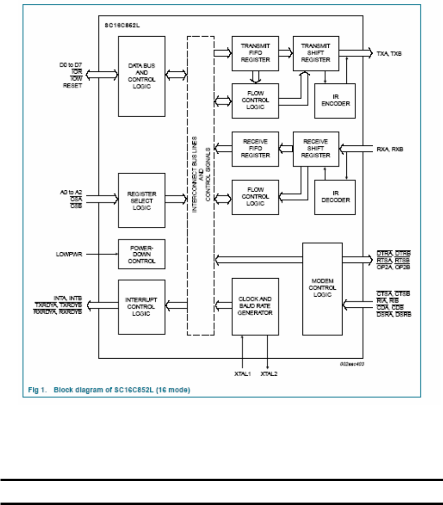
The one is the NXP SC16C852L, the other is EXAR XR16M2550. The function blocks and reference
schematics are shown below. For single external UART solution, please refer to section 6.2.
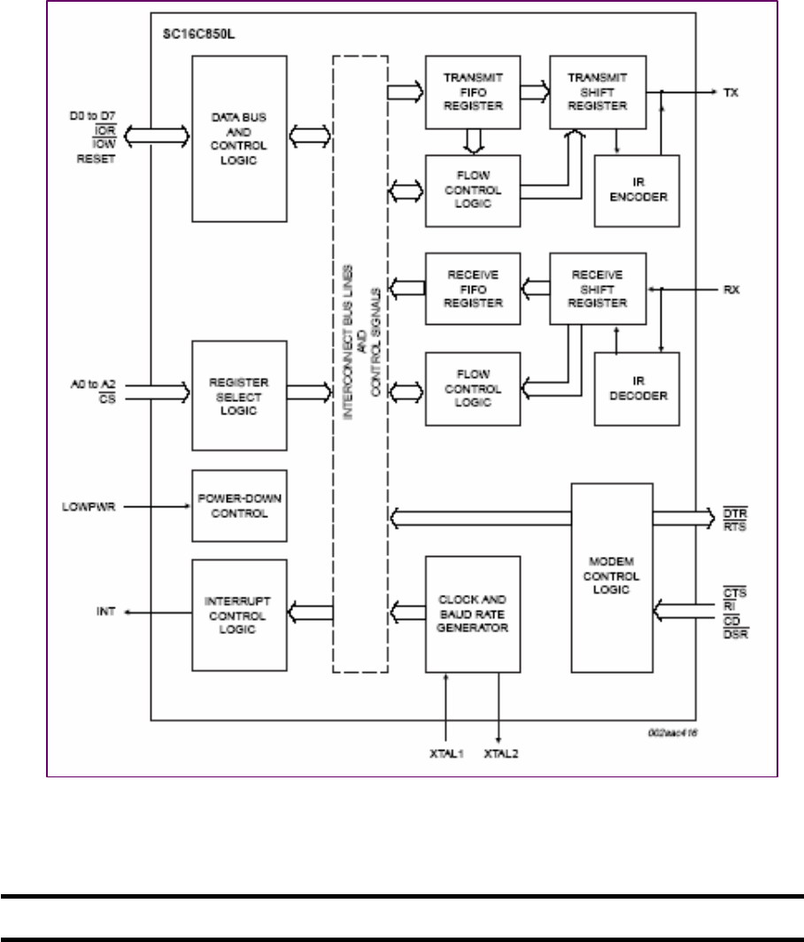
Dual UART interface NXP SC16C852L
1.8 V dual UART, 5 Mbit/s (max.) with 128-byte FIFOs, parallel bus interface
Package HVQFN32(5x5mm), LQFP48(9x9mm)
©2007 B e n Q C o r p o r a t i o n C o n f i d e n t i a l P r o p e r t y
M 27 U s e r M a n u a l V e r s i o n : 0. 1 - 2007/ J u l / 3 0
36
U5
PMGD280UN
S1
1
D2
3
G2 5
S2 4
G1
2
D1 6
UART_RXB
UART_TXB
3.3V
1.8V R13
10K J
R12
10K J
R14
10K J
R15
10K J
UART_CTSB
U6
PMGD280UN
S1
1
D2
3
G2 5
S2 4
G1
2
D1 6
3.3V
UART_RSTB
1.8V R19
10K J
R17
10K J
R20
10K J
R21
10K J
U1
EXAR XR16M2550 / NXP SC16C852L
D3
30
D0
27
D2
29 D1
28
D5
32
RTSA# 23
RXA 4
TXA 5
VCC 26
D4
31
CTSA# 25
D6
1
D7
2
A0
20
A1
19
A2
18
IOR#
14
IOW#
12
UART_CSA#
7
UART_CSB#
8
UART_INTA
22
UART_INTB
21
UART_RESET
24
TXB 6
RXB 3
RTSB# 15
GND
13
XTAL1
10
XTAL2
11
GND
33
NC
9
NC
17 CTSB# 16
D0
D1
D4
D3
D2
D6
D5
D7
A0
A2
A1
D[0..7]
A[0..2] A[0..2]
UART_CSA#
IOW#
IOR#
UART_INTA
UART_RESET
UART_CSB#
UART_INTB
R8 0 ohm
X1
24MHz
21
C7
22P J
C6
22P J
R11
576K J
D[0..7] 1.8V U2
PMGD280UN
S1
1
D2
3
G2 5
S2 4
G1
2
D1 6
UART_RXA
3.3V
UART_TXA
1.8V R2
10K J
R1
10K J
R4
10K J
R5
10K J
UART_CTSA
U4
PMGD280UN
S1
1
D2
3
G2 5
S2 4
G1
2
D1 6UART_RSTA
3.3V
1.8V R7
10K J
R6
10K J
R9
10K J
R10
10K J
Level shifter
Dual UART interface
EXAR XR16M2550
HIGH PERFORMANCE LOW VOLTAGE DUART WITH 16-BYTE FIFO
Package 32 PIN QFN(5x5mm), 48 PIN TQFP (9x9mm)
©2007 B e n Q C o r p o r a t i o n C o n f i d e n t i a l P r o p e r t y
M 27 U s e r M a n u a l V e r s i o n : 0. 1 - 2007/ J u l / 3 0
37
RS232_TX2
RS232_RX2
CTS
UART_TXA
UART_RXA
UART_RSTA
UART_TXB
R18
0 J 0603
RXD
CTS
DCD
DSR
RI
PC SIDE(DTE)
RXD
RTS
PC SIDE(DTE)
RTS
TXD
TXDDCD
RI
GND
DTR
3.3V_EXT 3,5,7,9
C1
10U 6.3V
3.3V
R3
0 J 0603
UART_CTSA
U3
ICL3237CA
VCC
26
GND
2
MBAUD
15
EN
13
T1IN
24
T2IN
23
T3IN
22
R1OUT
21
R2OUT
20
R3OUT
18
T4IN
19
T5IN
17
R1OUTB
16
SHDN
14
C1+ 28
C1- 25
C2+ 1
C2- 3
V+ 27
V- 4
T1OUT 5
T2OUT 6
T3OUT 7
R1IN 8
R2IN 9
R3IN 11
T4OUT 10
T5OUT 12
PORT1
D-SUB9 FEMALE
5
9
4
8
3
7
2
6
1
C2 0.47U M
UART_RXB
C3 0.47U M
C4 0.47U M
C5 0.47U M
M27 SIDE(DCE)
RS232_RX2
3.3V_EXT
R16
N/A
RS232_TX2
PORT2
D-SUB9 FEMALE
5
9
4
8
3
7
2
6
1
UART
UART
UART
UART
©2007 B e n Q C o r p o r a t i o n C o n f i d e n t i a l P r o p e r t y
M 27 U s e r M a n u a l V e r s i o n : 0. 1 - 2007/ J u l / 3 0
38
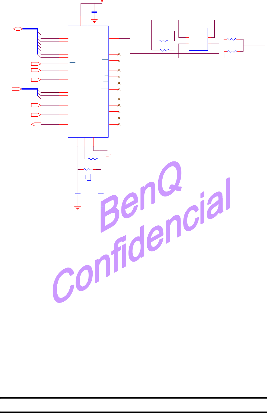
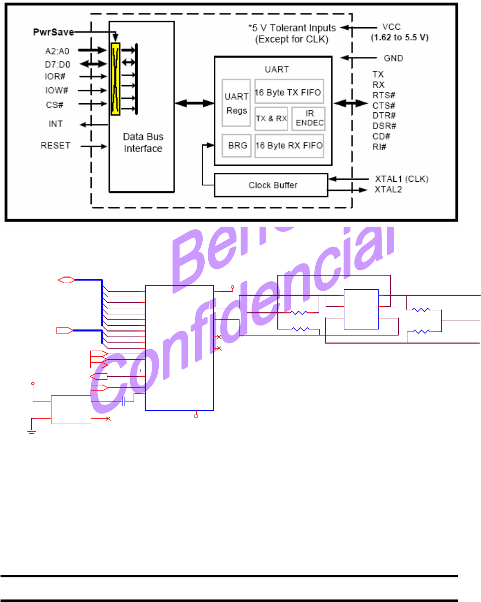
6.2 Single external UART solution
For single external UART solution, there are two options: the one is NXP SC16C850LIET, the other
is EXAR XR16L570IL24. The function block and reference schematics are shown below:
6.2.1 Single external UART solution: NXP SC16C850LIET
Single UART interface NXP SC16C850LIET
1.8 V single UART, 5 Mbit/s (max.) with 128-byte FIFOs parallel bus interface
Package TFBGA36(3.5x3.5mm), HVQFN32( 5x5mm)
©2007 B e n Q C o r p o r a t i o n C o n f i d e n t i a l P r o p e r t y
M 27 U s e r M a n u a l V e r s i o n : 0. 1 - 2007/ J u l / 3 0
39
U16
SC16C850LIET
VDD A1
N.C. A2
IOR
A3
N.C. A4
XTAL2
A5
XTAL1
A6
A2
B1
N.C. B2
N.C. B3
IOW
B4
LOWPWR
B5
CS
B6
A0
C1
VSS
C2
A1
C3
VSS
C4
TX C5
RX C6
INT
D1
RTS D2
VDD D4
D7
D5 D6
D6
DSR F2
N.C. E2
CD E3
D1
E4
D3
E5
D5
E6
RESET
F1
DTR E1
RI F3
D0
F4
D2
F5
D4
F6
CTS D3
D0
D1
D3
D2
D4
D5
D7
D6
A0
A1
A2
D[0..7]
A[0..2] A[0..2]
D[0..7]
IOW#
IOR#
UART_RESET
Note : UART_TXA, UART_RXA, UART_RSTA,
UART_CTSA are from M27
X3
24MHz
21
C28
22P J
C27
22P J
R58
576K J
R57 0 ohm
UART_CSA#
UART_INTA
UART_LOWPWR
C22
0.1U K
1.8V
UART_RXB
U18
PMGD280UN
S1
1
D2
3
G2 5
S2 4
G1
2
D1 6
3.3V
UART_TXB
1.8V R52
10K J
R51
10K J
R53
10K J
R54
10K J
©2007 B e n Q C o r p o r a t i o n C o n f i d e n t i a l P r o p e r t y
M 27 U s e r M a n u a l V e r s i o n : 0. 1 - 2007/ J u l / 3 0
40
6.2.2 Single external UART solution: EXAR XR16L570IL24
UART_INTA
1.8V
UART_RXB
U14
PMGD280UN
S1
1
D2
3
G2 5
S2 4
G1
2
D1 6
3.3V
UART_TXB
1.8V R45
10K J
R44
10K J
R46
10K J
R47
10K J
C20
0.047U K
Y1
24MHZ
Cont 1
GND
2
OUT 3
VDD
4
U13 XR16L570IL24
D3
23
D0
20
D2
22 D1
21
D5
1RXA 4
TXA 5
VCC 19
D4
24
CTS# 18
D6
2
D7
3
A0
14
A1
13
A2
12
IOR#
11
IOW#
9
UART_CS#
6
UART_INT
15
UART_RESET
17
PwrSave
7
CLK
8
GND
10
RTS# 16
3.3V
D0
D1
D4
D3
D2
D6
D5
D7
A0
A2
A1
D[0..7]
IOR#
A[0..2] A[0..2]
D[0..7]
IOW#
UART_CSA#
UART_RESET
Single UART interface EXAR XR16L570IL24
SMALLEST 1.62V TO 5.5V UART WITH 16-BYTE FIFO AND POWERSAVE
Package 24 PIN QFN(4x4mm), 32 PIN QFN(5x5mm)
©2007 B e n Q C o r p o r a t i o n C o n f i d e n t i a l P r o p e r t y
M 27 U s e r M a n u a l V e r s i o n : 0. 1 - 2007/ J u l / 3 0
41
7 USB Interface
USB signals are transmitted on a twisted pair of data cables, labeled D+ and D−. These collectively
use half-duplex differential signaling to combat the effects of electromagnetic noise on longer lines. D+
and D− usually operate together; They are not separate simplex connections. Transmitted signal levels
are 0.0–0.3 volts for low and 2.8–3.6 volts for high.
The USB supports three data rates
- Low Speed rate of 1.5 M bit/s (183 KiB/s).
- Full Speed rate of 12 M bit/s (1.5 MiB/s).
USB connector pin out
Pin Mini Function M27
1 V
BUS
(4.4–5.25 V) V
BUS
(2.7–5.25 V)
2 D− USB_DM
3 D+ USB_DP
4 ID
5 Ground Ground
Pin Name Pin Out Pull Reset Config
Description
VBUS 16 PD Power Supply VBUS line
USB_DP 18 USB data bus (positive terminal)
USB_DM 20 USB data bus (negative terminal)
Note: The difference between Reset and Config in the pin definition table
M27 Host Device EVB
VBUS
USB_DM
USB_DP
ID
GND
VBUS
USB_DM
USB_DP
GND
VBUS
USB_DM
USB_DP
ID
GND
©2007 B e n Q C o r p o r a t i o n C o n f i d e n t i a l P r o p e r t y
M 27 U s e r M a n u a l V e r s i o n : 0. 1 - 2007/ J u l / 3 0
42
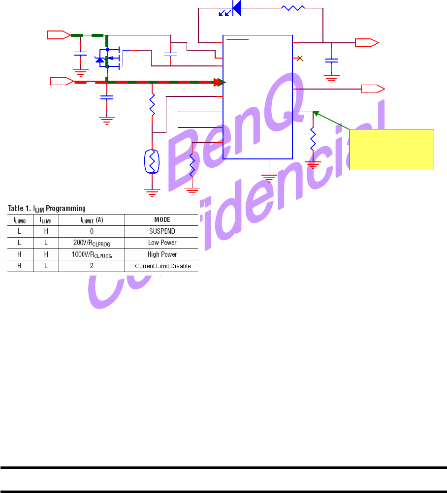
7.1 USB charger solution
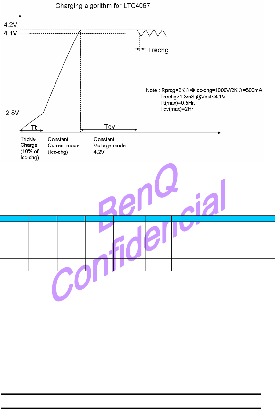
For USB charger application, our suggestion is to use the Linear Technology LTC4067 as the
Li-ion battery charger.
This chip manages the power supplies that would be typical for a USB powered device or from an
adaptor to an intermediate voltage bus. The battery charger is a CC/CV timer terminated type capable of
charge currents up to 1.25A. The adaptor input has over-voltage protection to 13V. An external MOSFET
will disconnect the adaptor if the voltage exceeds 6V; protecting the input against damage in case an
unregulated adaptor is accidentally plugged in.
U8 LTC4067EDE
ILIM0
4
CHRG
2
NTC
3
IN
12
CLPROG
1
GND
13
PROG 8
OVI
6
BAT 10
GATE 9
OUT 11
ILIM1
5
OVP
7
TR1
TR_10K
(0402)
R26
10K J
12
GSM/GPRS module
1 Cell Li-ion battery
C125
0.01U K
C108
0.47U K
Q2 SI2343DS
R28
2K J
ILIM0
ILIM1
Wall input
4.35V~6V
C14
10U 6.3V
D1
C192TBKT-B
12 R25
100 J
R27
2K J
C13
10U 6.3V
VBUS
Note : ILIM0,ILIM1 are 1.8V interface
Actual charge current
Ibat=Vprog/2kӨ
©2007 B e n Q C o r p o r a t i o n C o n f i d e n t i a l P r o p e r t y
M 27 U s e r M a n u a l V e r s i o n : 0. 1 - 2007/ J u l / 3 0
43
8 GPIO MAPPING
The module provides 4 independent GPIO pins configurable in read or write mode. The function for
these I/O pins is List below.
Pin Name
Pin No I/O PU Reset Config
Description
GPIO 1
87 I/O PU Input Low
General purpose I/O 1
GPIO 10
60 I/O PU Input Low
General purpose I/O 10
GPIO 14
34 I/O PD Input Low
General purpose I/O 14
GPIO 37
32 I/O Input Float
General purpose I/O 37
©2007 B e n Q C o r p o r a t i o n C o n f i d e n t i a l P r o p e r t y
M 27 U s e r M a n u a l V e r s i o n : 0. 1 - 2007/ J u l / 3 0
44
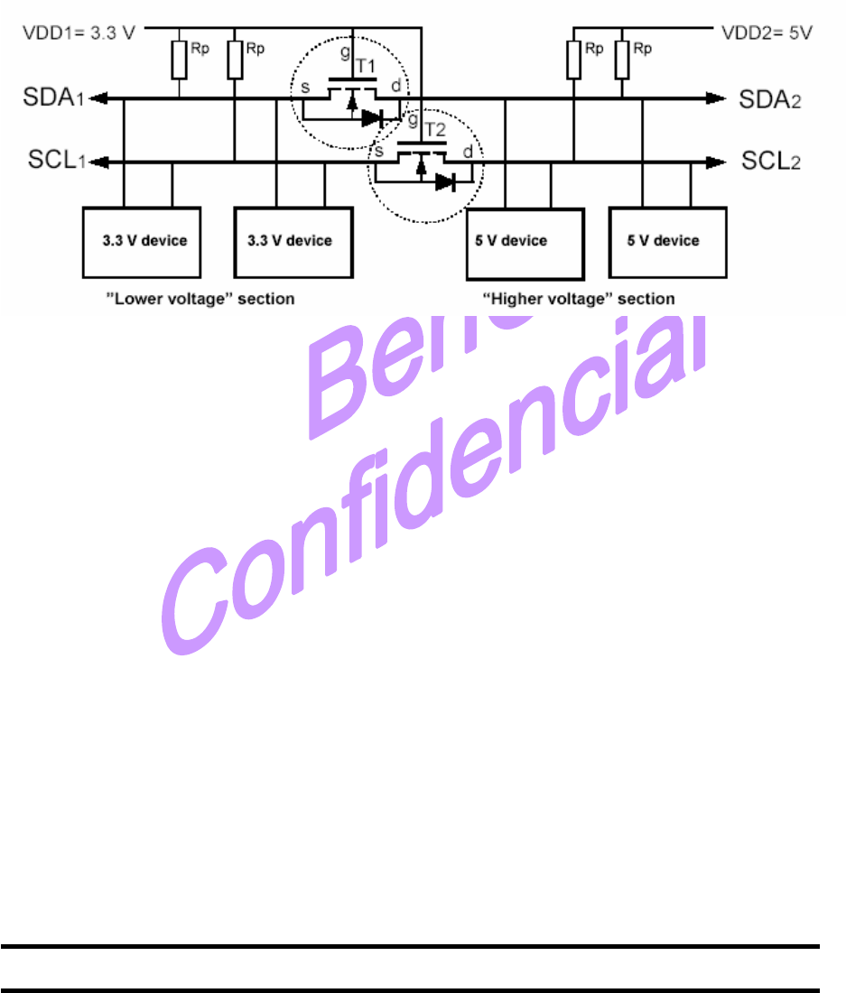
9
Level Shifter Design
9.1 Introduction
The bi-directional level shifter circuit described in this application note consists of one discrete
MOS-FET for each bus line. In spite of its surprising simplicity, it not only fulfils the requirement of
bi-directional level shifting without a direction control signal, but it also has the next additional features:
- Isolating of a powered-down bus section from the rest of the bus system,
- Protection of the “Lower voltage” side against high voltage spikes at the ‘Higher voltage” side.
The bi-directional level shifter can be used in standard mode (0 to 100 kbit/s) or in fast mode (0 to 400
kbit/s) I2C-bus systems, without any change. The following descriptions apply for both modes.

©2007 B e n Q C o r p o r a t i o n C o n f i d e n t i a l P r o p e r t y
M 27 U s e r M a n u a l V e r s i o n : 0. 1 - 2007/ J u l / 3 0
45
10. Layout notice
10.1 THT hole and pad size for 2x7 connector
©2007 B e n Q C o r p o r a t i o n C o n f i d e n t i a l P r o p e r t y
M 27 U s e r M a n u a l V e r s i o n : 0. 1 - 2007/ J u l / 3 0
46
11. Antenna Interface
11.1 Antenna Installation & Consideration
M27 is capable of sustaining a total mismatch at the antenna pad without any damage, even when
transmitting at maximum RF power. The RF interface has an impedance of 50Ω. M27 must be applied
to 50 ohm load/ antenna, or else the output power will degrade seriously. Antenna supplier needs to
ensure that the impedance of the operating frequency range is closed to 50Ω.
The external antenna must be matched properly to achieve best performance regarding radiated
power, DC-power consumption, modulation accuracy and harmonic suppression. Antenna matching
networks are not included on the M27 PCB and should be placed in the host application.
Due to the Antenna selection is more important for the wireless performance, this application will
provide the Antenna requirements for mobile quad-band modules (GSM850. EGSM, DCS and PCS)
(Table11.1~Table11.4).
Table11.1. Frequency Bands
Item Description Requirement
1 Transmit Bands (TX)
GSM850: 869 ~ 894 MHz
EGSM: 880 ~ 915 MHz
DCS: 1710 ~ 1785 MHz
PCS: 1850 ~ 1910 MHz
2 Receive Bands (RX)
GSM850: 824 ~ 849 MHz
EGSM: 925 ~ 960 MHz
DCS: 1805 ~ 1880 MHz
PCS: 1930 ~ 1990 MHz
Table11.2. VSWR
Item Description Requirement
1 VSWR Љ
ЉЉ
Љʳ
ʳʳ
ʳ2 : 1
2 Measurement
Network analyzer
is used to measure
VSWR, and
the result must be measured
with the matching circuit provided by
Antenna vendor.
©2007 B e n Q C o r p o r a t i o n C o n f i d e n t i a l P r o p e r t y
M 27 U s e r M a n u a l V e r s i o n : 0. 1 - 2007/ J u l / 3 0
47
Table11.3. Gain
Item Description Requirement
1 Average gain Њ
ЊЊ
Њ 0 dBi
2 Peak gain
Њ
ЊЊ
Њ 0.5 dBi
The gain deviation (Peak gain –
minimum
gain) of all angles in H-
plane should be less
than 4dB in low, middle and high channels.
The higher gain in DCS/PCS
band would
be preferred.
3 Measurement
The same as the Table11.2 item2. mea
sure
the radiation pattern at
the lowest, middle
and highest frequency for each band.
And it
must be measured in Chamber, including
XY, XZ and YZ planes.
Table11.4. Power Rating
Item Description Requirement
1 .Maximum Value: 2W(CW)
2 Measuring Method
A 50Ө coaxial cable is connected to the 50
Ө
feeding point on the PCB. The power is
applied for 10 minutes at the middle
frequency of each Tx band. After the test
then measure the VSWR.
3 Criteria
The antenna shall satisfy the VSWR as
described in Table11.2. No visual deteriora-
tion shall occur during or after the test.
©2007 B e n Q C o r p o r a t i o n C o n f i d e n t i a l P r o p e r t y
M 27 U s e r M a n u a l V e r s i o n : 0. 1 - 2007/ J u l / 3 0
48
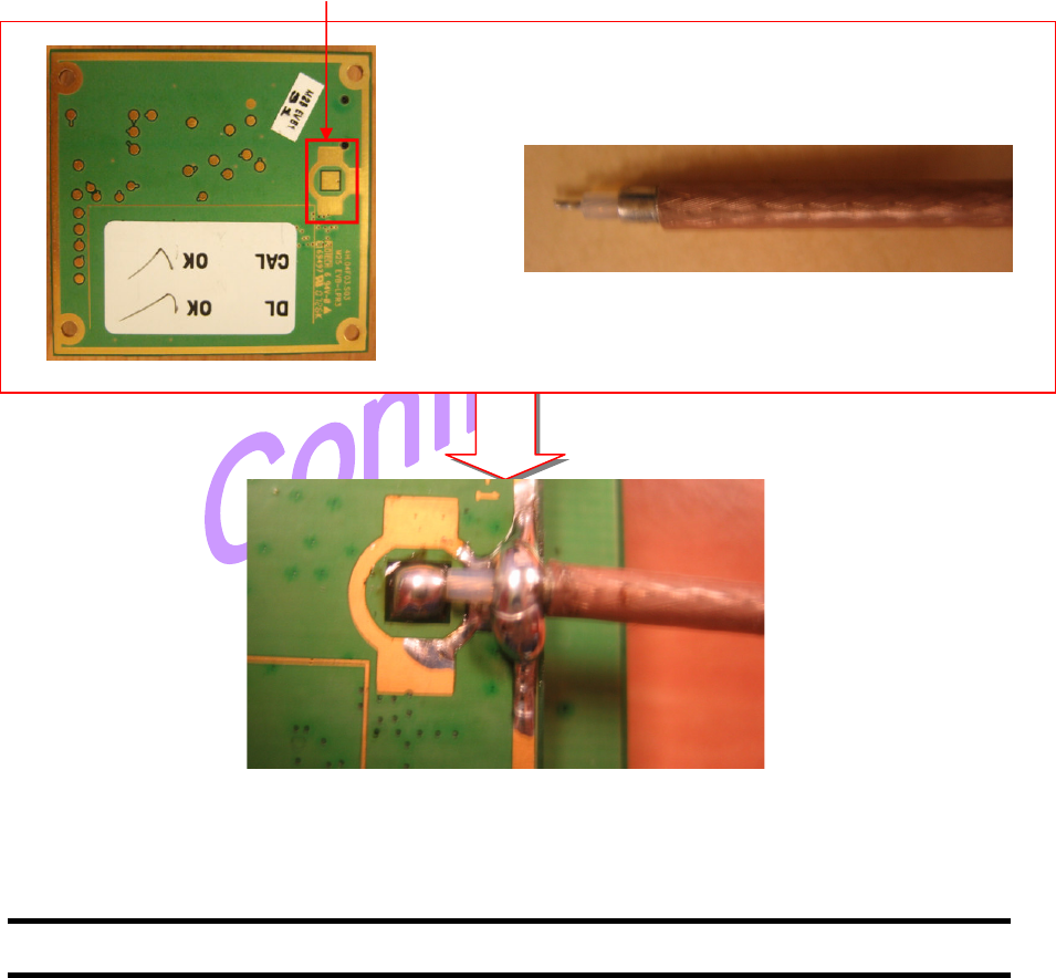
11.2 Antenna Pad & Cable S
oldering
The antenna can be soldered to the antenna pad. For proper grounding connect the
antenna to the ground plane on the bottom of M27 which must be connected to the ground
plane of the application.(Fig.11.1)
Notes on soldering:
To prevent damage to the module and to obtain long-term solder joint properties you are
advised to maintain the standards of good engineering practice for soldering.
Be sure to solder the antenna core to the pad and the shielding of the coax cable to the
ground plane of the module next to the antenna pad. The direction of the cable is not
relevant from the electrical point of view.
M27 material properties:
M27 PCB: FR4
Antenna pad: Gold plated pad
Fig.11.1 Antenna Pad & Cable Soldering
Antenna Pad
Antenna Cable

©2007 B e n Q C o r p o r a t i o n C o n f i d e n t i a l P r o p e r t y
M 27 U s e r M a n u a l V e r s i o n : 0. 1 - 2007/ J u l / 3 0
49
˙ ˖ ˖ ʳ˜ ˗ ˍ ʳ˩ ˥ ˦ ˠ ˅ ˊ
˙ ˖ ˖ ʳ˜ ˗ ˍ ʳ˩ ˥ ˦ ˠ ˅ ˊ˙ ˖ ˖ ʳ˜ ˗ ˍ ʳ˩ ˥ ˦ ˠ ˅ ˊ
˙ ˖ ˖ ʳ˜ ˗ ˍ ʳ˩ ˥ ˦ ˠ ˅ ˊ ʳ
ʳʳ
ʳ
˧ ˻ ˼ ̆ ʳ˷ ˸ ̉ ˼ ˶ ˸ ʳ˶ ̂ ̀ ̃ ˿ ˼ ˸ ̆ ʳ̊ ˼ ̇ ˻ ʳˣ ˴ ̅ ̇ ʳ˄ ˈ ʳ̂ ˹ ʳ̇ ˻ ˸ ʳ˙ ˖ ˖ ʳ˥ ̈ ˿ ˸ ̆ ˁʳˢ ̃ ˸ ̅ ˴ ̇ ˼ ̂ ́ ʳ˼ ̆ ʳ̆ ̈ ˵ ˽ ˸ ˶ ̇ ʳ̇ ̂ ʳ̇ ˻ ˸ ʳ˹ ̂ ˿ ˿ ̂ ̊ ˼ ́ ˺ ʳ̇ ̊ ̂ ʳ
˶ ̂ ́ ˷ ˼ ̇ ˼ ̂ ́ ̆ ˍ ʳ
˄ ˁ̇ ˻ ˼ ̆ ʳ˷ ˸ ̉ ˼ ˶ ˸ ʳ̀ ˴ ̌ ʳ́ ̂ ̇ ʳ˶ ˴ ̈ ̆ ˸ ʳ˻ ˴ ̅ ̀ ˹ ̈ ˿ ʳ˼ ́ ̇ ˸ ̅ ˹ ˸ ̅ ˸ ́ ˶ ˸ ʿ ʳ˴ ́ ˷ ʳ
˅ ˁ̇ ˻ ˼ ̆ ʳ˷ ˸ ̉ ˼ ˶ ˸ ʳ̀ ̈ ̆ ̇ ʳ˴ ˶ ˶ ˸ ̃ ̇ ʳ˴ ́ ̌ ʳ˼ ́ ̇ ˸ ̅ ˹ ˸ ̅ ˸ ́ ˶ ˸ ʳ̅ ˸ ˶ ˸ ˼ ̉ ˸ ˷ ʿ ʳ˼ ́ ˶ ˿ ̈ ˷ ˼ ́ ˺ ʳ˼ ́ ̇ ˸ ̅ ˹ ˸ ̅ ˸ ́ ˶ ˸ ʳ̇ ˻ ˴ ̇ ʳ̀ ˴ ̌ ʳ˶ ˴ ̈ ̆ ˸ ʳ̈ ́ ˷ ˸ ̆ ˼ ̅ ˸ ˷ ʳ
̂ ̃ ˸ ̅ ˴ ̇ ˼ ̂ ́ ˁʳ
˖ ˻ ˴ ́ ˺ ˸ ̆ ʳ̂ ̅ ʳ̀ ̂ ˷ ˼ ˹ ˼ ˶ ˴ ̇ ˼ ̂ ́ ̆ ʳ́ ̂ ̇ ʳ˸ ̋ ̃ ̅ ˸ ̆ ̆ ˿ ̌ ʳ˴ ̃ ̃ ̅ ̂ ̉ ˸ ˷ ʳ˵ ̌ ʳ̇ ˻ ˸ ʳ̃ ˴ ̅ ̇ ̌ ʳ̅ ˸ ̆ ̃ ̂ ́ ̆ ˼ ˵ ˿ ˸ ʳ˹ ̂ ̅ ʳ˶ ̂ ̀ ̃ ˿ ˼ ˴ ́ ˶ ˸ ʳ˶ ̂ ̈ ˿ ˷ ʳ̉ ̂ ˼ ˷ ʳ
̇ ˻ ˸ ʳ̈ ̆ ˸ ̅ ʺ ̆ ʳ˴ ̈ ̇ ˻ ̂ ̅ ˼ ̇ ̌ ʳ̇ ̂ ʳ̂ ̃ ˸ ̅ ˴ ̇ ˸ ʳ̇ ˻ ˸ ʳ˸ ̄ ̈ ˼ ̃ ̀ ˸ ́ ̇ ˁʳ
ˠ ˴ ̋ ˼ ̀ ̈ ̀ ʳ˴ ́ ̇ ˸ ́ ́ ˴ ʳ˺ ˴ ˼ ́ ʳ˴ ˿ ˿ ̂ ̊ ˸ ˷ ʳ˹ ̂ ̅ ʳ̈ ̆ ˸ ʳ̊ ˼ ̇ ˻ ʳ̇ ˻ ˼ ̆ ʳ˷ ˸ ̉ ˼ ˶ ˸ ʳ˼ ̆ ʳ˃ ˷ ˕ ˼ ˁʳ
˪ ˻ ˸ ́ ʳ̇ ˻ ˸ ʳ̀ ̂ ˷ ̈ ˿ ˸ ʳ˼ ̆ ʳ˼ ́ ̆ ̇ ˴ ˿ ˿ ˸ ˷ ʳ˼ ́ ʳ̇ ˻ ˸ ʳ˻ ̂ ̆ ̇ ʳ˷ ˸ ̉ ˼ ˶ ˸ ʿ ʳ̇ ˻ ˸ ʳ˙ ˖ ˖ ʳ˜ ˗ ʳ˿ ˴ ˵ ˸ ˿ ʳ̀ ̈ ̆ ̇ ʳ˵ ˸ ʳ̉ ˼ ̆ ˼ ˵ ˿ ˸ ʳ̇ ˻ ̅ ̂ ̈ ˺ ˻ ʳ˴ ʳ̊ ˼ ́ ˷ ̂ ̊ ʳ
̂ ́ ʳ̇ ˻ ˸ ʳ˹ ˼ ́ ˴ ˿ ʳ˷ ˸ ̉ ˼ ˶ ˸ ʳ̂ ̅ ʳ˼ ̇ ʳ̀ ̈ ̆ ̇ ʳ˵ ˸ ʳ̉ ˼ ̆ ˼ ˵ ˿ ˸ ʳ̊ ˻ ˸ ́ ʳ˴ ́ ʳ˴ ˶ ˶ ˸ ̆ ̆ ʳ̃ ˴ ́ ˸ ˿ ʿ ʳ˷ ̂ ̂ ̅ ʳ̂ ̅ ʳ˶ ̂ ̉ ˸ ̅ ʳ˼ ̆ ʳ˸ ˴ ̆ ˼ ˿ ̌ ʳ̅ ˸ ˀ̀ ̂ ̉ ˸ ˷ ˁʳ˜ ˹ ʳ
́ ̂ ̇ ʿ ʳ˴ ʳ̆ ˸ ˶ ̂ ́ ˷ ʳ˿ ˴ ˵ ˸ ˿ ʳ̀ ̈ ̆ ̇ ʳ˵ ˸ ʳ̃ ˿ ˴ ˶ ˸ ˷ ʳ̂ ́ ʳ̇ ˻ ˸ ʳ̂ ̈ ̇ ̆ ˼ ˷ ˸ ʳ̂ ˹ ʳ̇ ˻ ˸ ʳ˹ ˼ ́ ˴ ˿ ʳ˷ ˸ ̉ ˼ ˶ ˸ ʳ̇ ˻ ˴ ̇ ʳ˶ ̂ ́ ̇ ˴ ˼ ́ ̆ ʳ̇ ˻ ˸ ʳ˹ ̂ ˿ ˿ ̂ ̊ ˼ ́ ˺ ʳ̇ ˸ ̆ ̇ ˍ ʳ
Ϙ˖ ̂ ́ ̇ ˴ ˼ ́ ̆ ʳ˙ ˖ ˖ ʳ˜ ˗ ˍ ʳ˩ ˥ ˦ ˠ ˅ ˊ ϙˁʳ