Quectel Wireless Solutions 201508UG96 UMTS/HSPA Module User Manual
Quectel Wireless Solutions Company Limited UMTS/HSPA Module
UserManual.wiki
>
Quectel Wireless Solutions
>
201508UG96 User Manual
User Manual
Navigation menu
Upload a User Manual
Namespaces
Wiki Guide
HTML
PDF
Info
Views
User Manual
Discussion / Help
Navigation
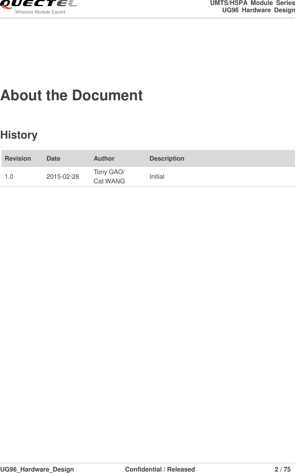
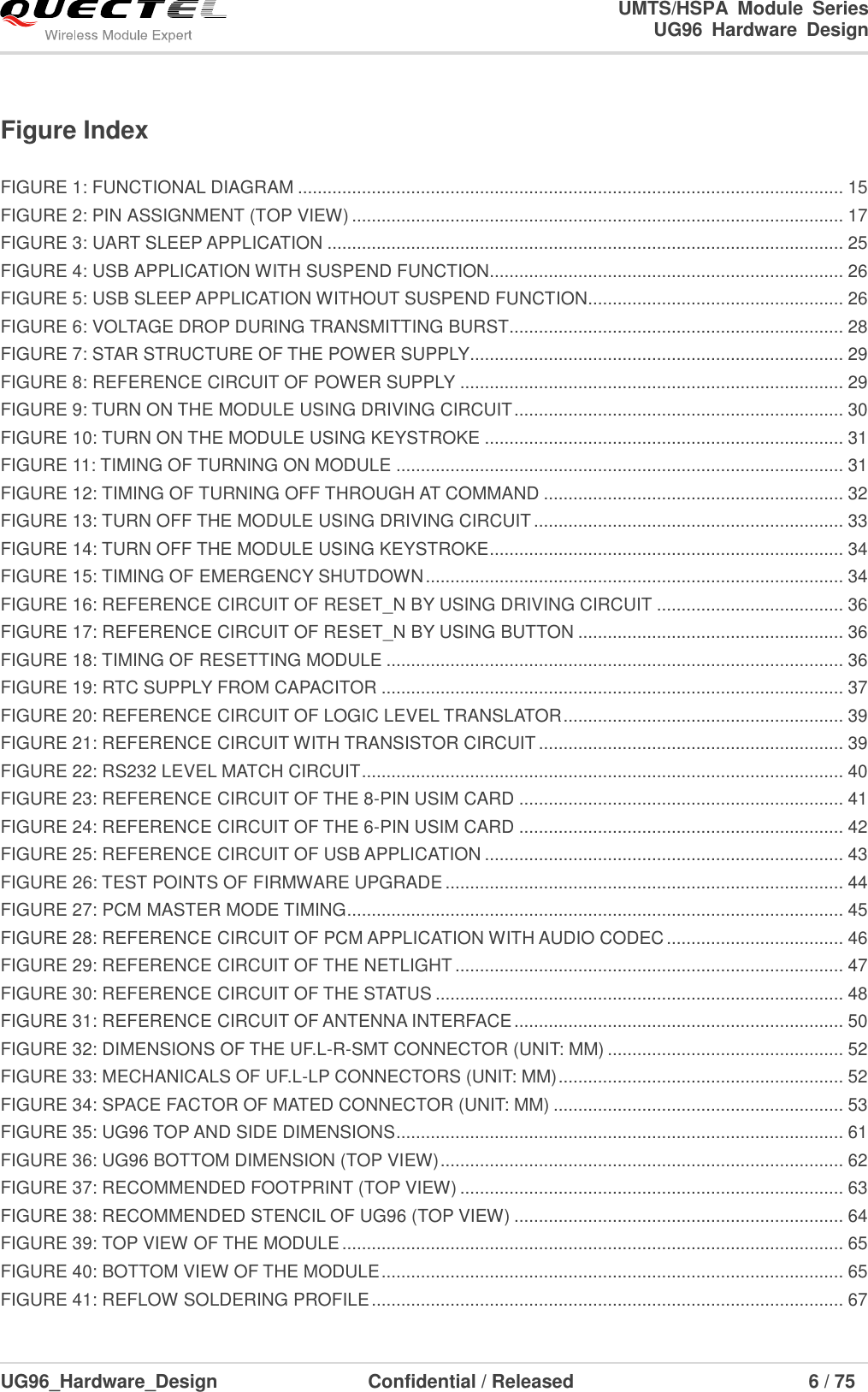
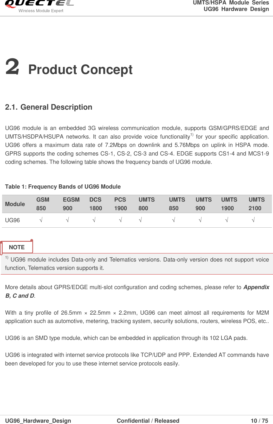
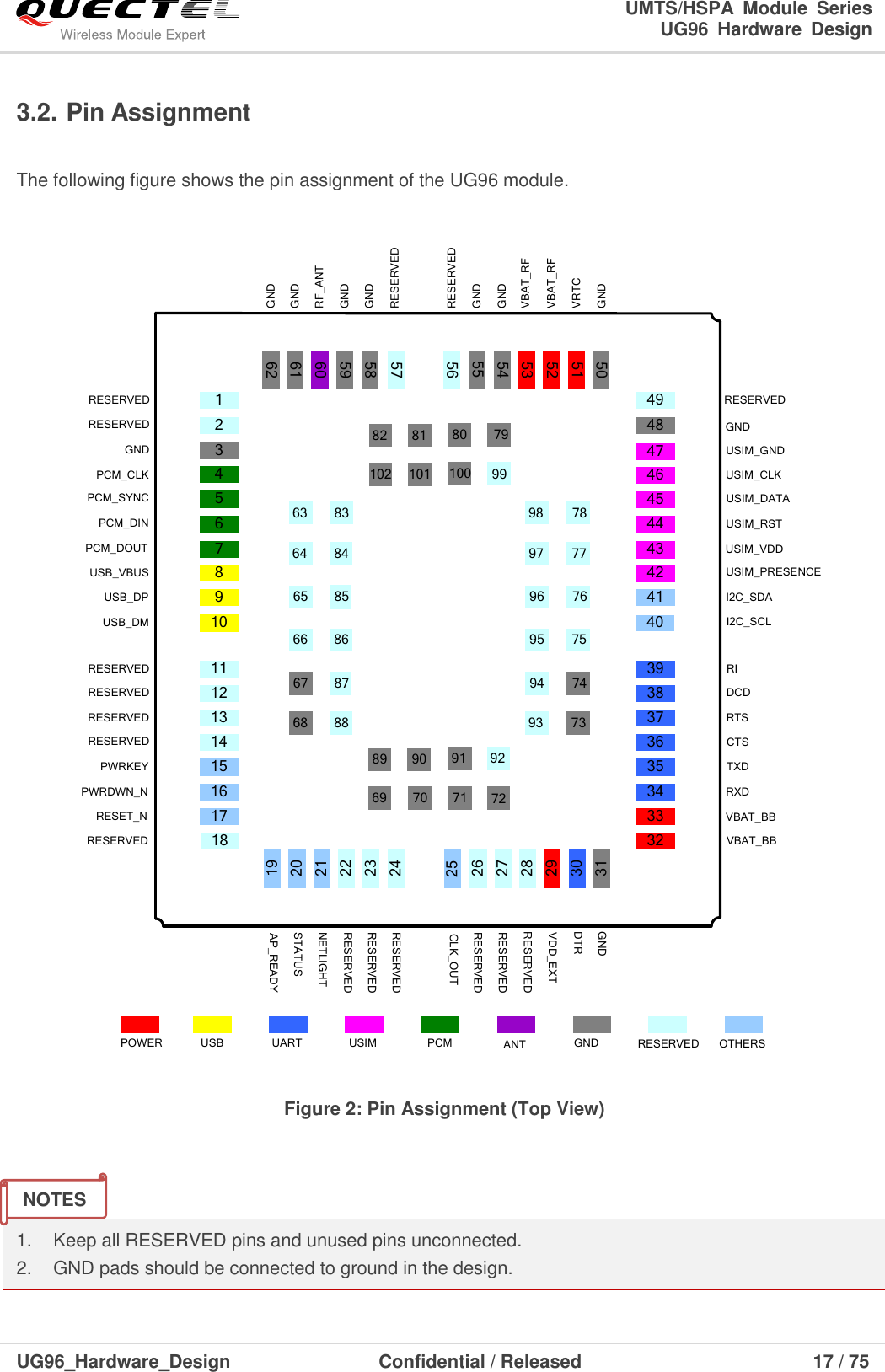
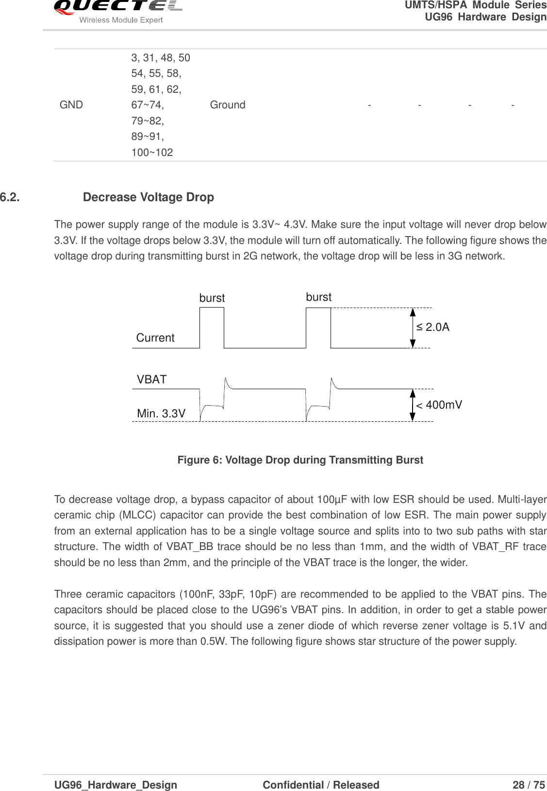
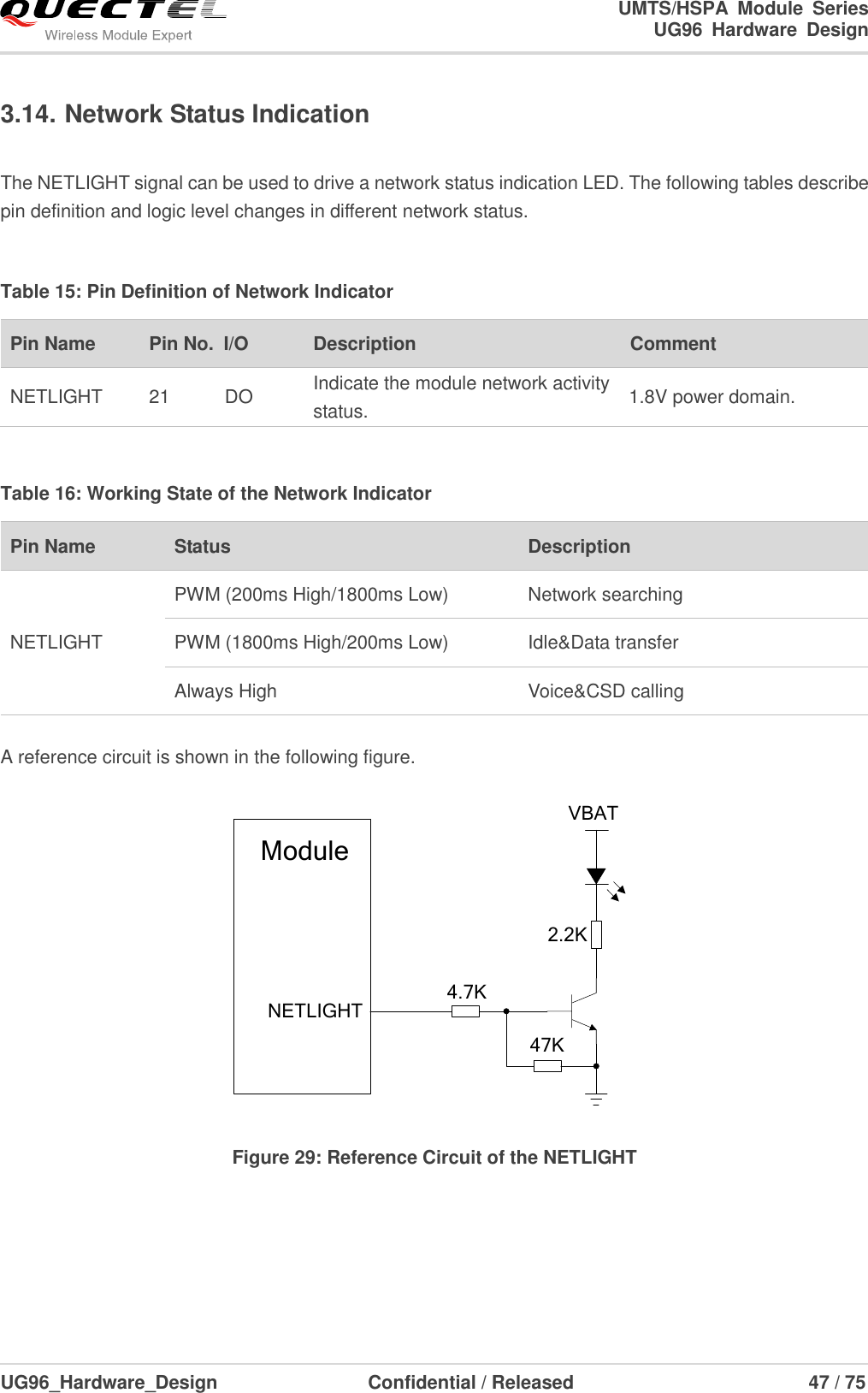
![UMTS/HSPA Module Series UG96 Hardware Design UG96_Hardware_Design Confidential / Released 15 / 75 PWRKEYRESET_N 32kHz PMU BasebandMCPRF_ANTUSIMSTATUSUARTVBAT_BBUSBVBAT_RFB1VDD_EXTVRTCNand+DDR PWRDWN_NRF TransceiverNETLIGHT26MHzDCXOB2/PCS1900GSM TX LBDuplexerPCMPMUResetI2CPA ASMB5/B6/GSM850B8/GSM900DC/DCB1B2B5/B6B8PM_HPM_LGSM TX HBDCS1800 Figure 1: Functional Diagram 2.5. Evaluation Board In order to help you to develop applications with UG96, Quectel supplies an evaluation board (UMTS&LTE-EVB), RS-232 to USB cable, USB data cable, power adapter, earphone, antenna and other peripherals to control or test the module. For details, please refer to document [2].](https://usermanual.wiki/Quectel-Wireless-Solutions/201508UG96/User-Guide-2705447-Page-16.png)
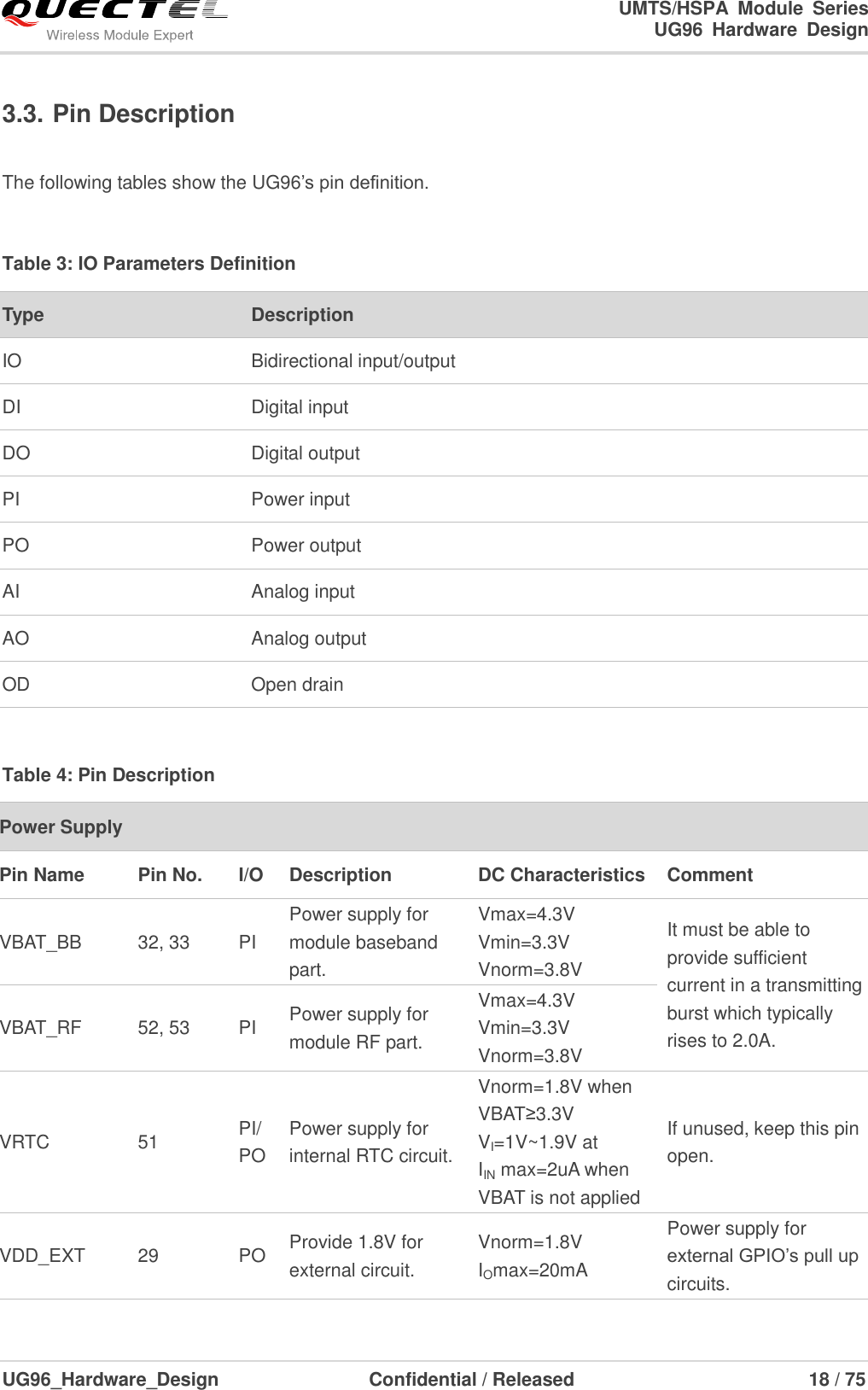
![UMTS/HSPA Module Series UG96 Hardware Design UG96_Hardware_Design Confidential / Released 27 / 75 1. In sleep mode, the module can still receive paging message, SMS, voice call and TCP/UDP data from the network normally. 2. The function of AP_READY is under development. 3.5.2. Minimum Functionality Mode Minimum functionality mode reduces the functionality of the module to minimum level, thus minimizes the current consumption at the same time. This mode can be set as below: Command AT+CFUN provides the choice of the functionality levels: <fun>=0, 1, 4. AT+CFUN=0: Minimum functionality, RF part and USIM card will be closed. AT+CFUN=1: Full functionality (by default). AT+CFUN=4: Disable RF function (airplane mode). All AT commands related to RF function are not accessible. For detailed information about command AT+CFUN, please refer to document [1]. 3.6. Power Supply 3.6.1. Power Supply Pins UG96 provides four VBAT pins dedicated to connect with the external power supply. There are two separate voltage domains for VBAT. VBAT_RF with two pads for module RF. VBAT_BB with two pads for module baseband. The following table shows the VBAT pins and ground pins. Table 6: VBAT and GND Pins Pin Name Pin No. Description Min. Typ. Max. Unit VBAT_RF 52, 53 Power supply for module RF part. 3.3 3.8 4.3 V VBAT_BB 32, 33 Power supply for module baseband part. 3.3 3.8 4.3 V NOTES](https://usermanual.wiki/Quectel-Wireless-Solutions/201508UG96/User-Guide-2705447-Page-28.png)
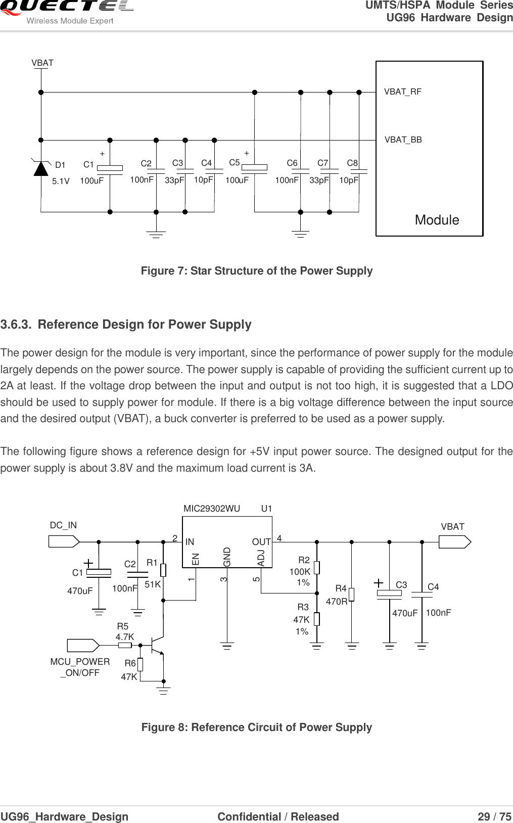
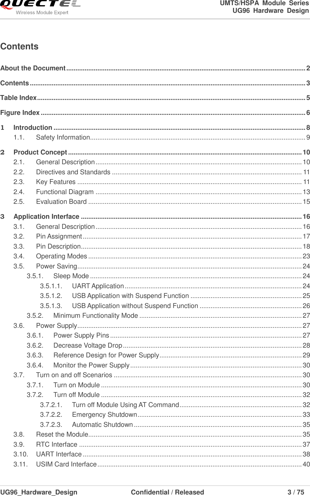
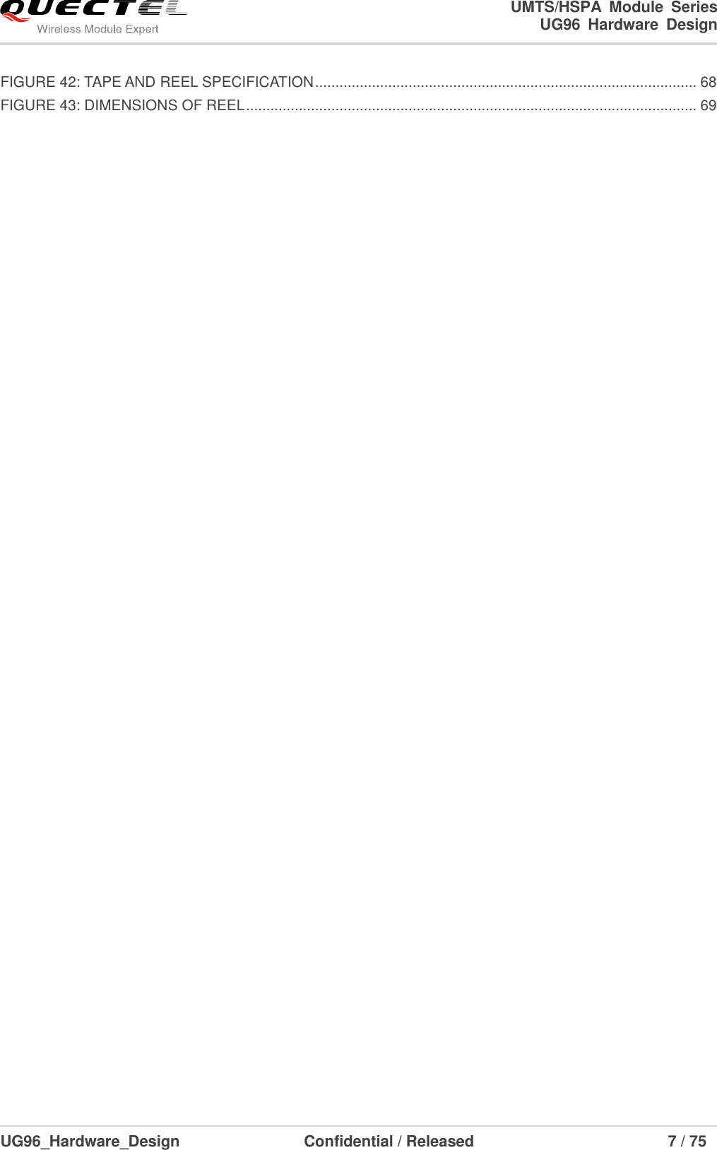
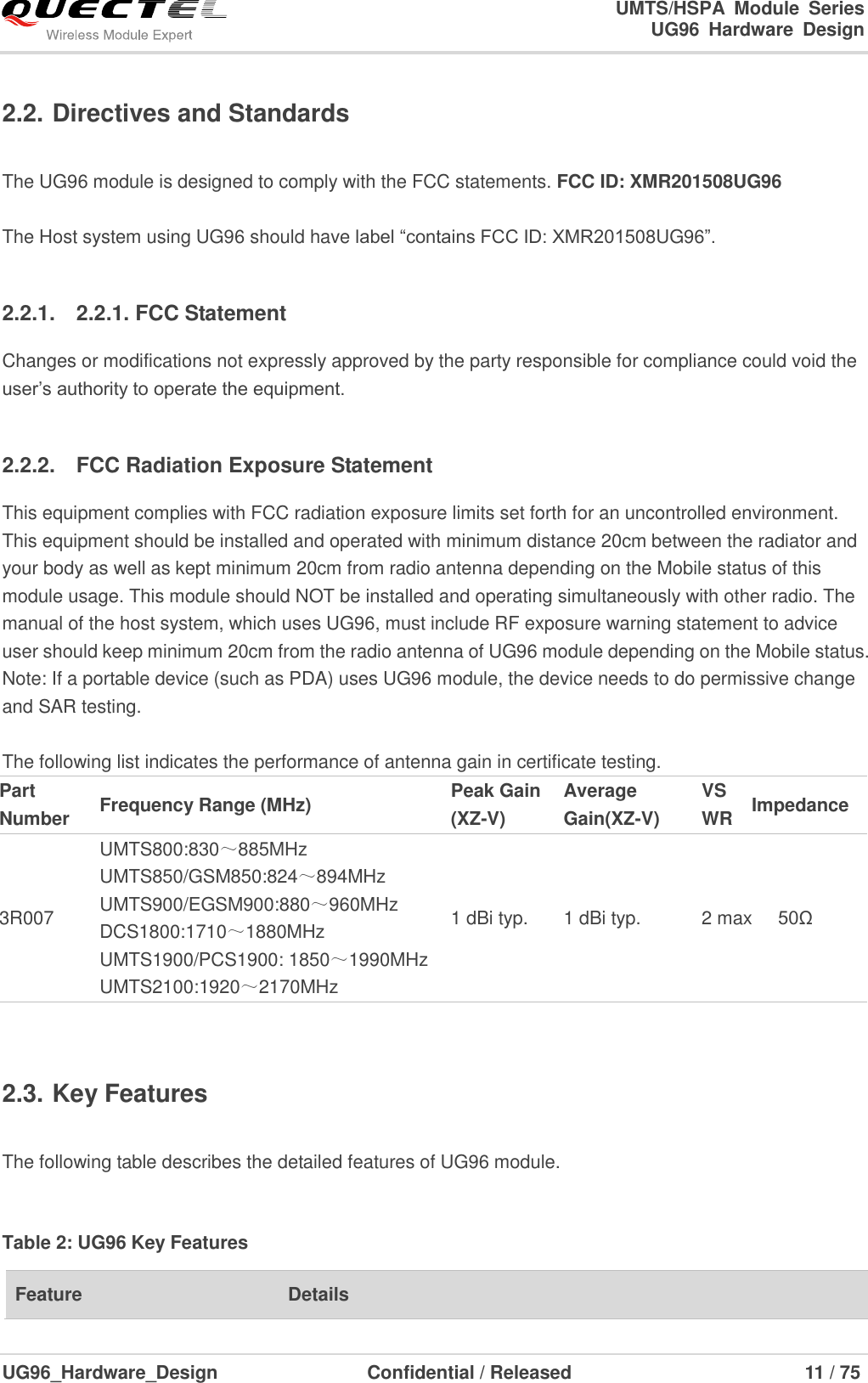
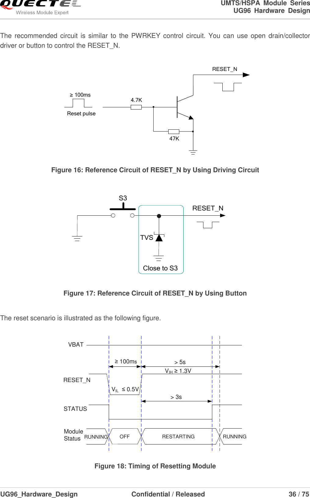
![UMTS/HSPA Module Series UG96 Hardware Design UG96_Hardware_Design Confidential / Released 30 / 75 It is suggested that you should switch off power supply for module in abnormal state, and then switch on power to restart module. 3.6.4. Monitor the Power Supply The command AT+CBC can be used to monitor the VBAT_BB voltage value displayed in millivolt. For more details, please refer to document [1]. 3.7. Turn on and off Scenarios 3.7.1. Turn on Module Turn on the module using the PWRKEY. The following table shows the pin definition of PWRKEY. Table 7: PWRKEY Pin Description Pin Name Pin No. Description DC Characteristics Comment PWRKEY 15 Turn on the module. VIHmax=2.1V VIHmin=1.3V VILmax=0.5V Pull-up to VRTC internally with 200kΩ resistor. When UG96 is in power down mode, it can be turned on to normal mode by driving the PWRKEY pin to a low level at least 100ms. It is recommended to use an open drain/collector driver to control the PWRKEY. The STATUS pin output a high level after UG96 is turned on. A simple reference circuit is illustrated in the following figure. Turn on pulsePWRKEY4.7K47K≥ 100ms Figure 9: Turn on the Module Using Driving Circuit NOTE](https://usermanual.wiki/Quectel-Wireless-Solutions/201508UG96/User-Guide-2705447-Page-31.png)
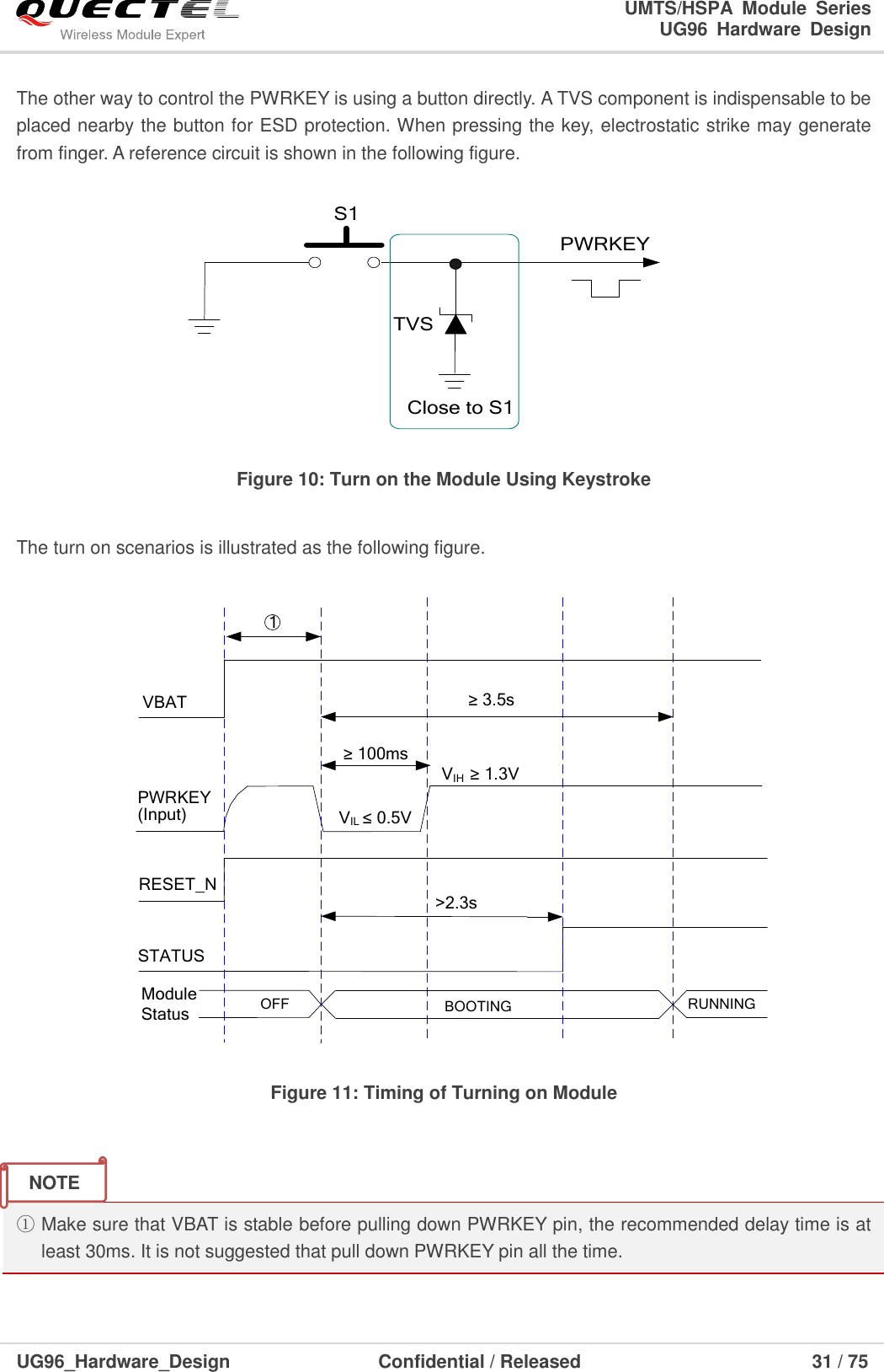
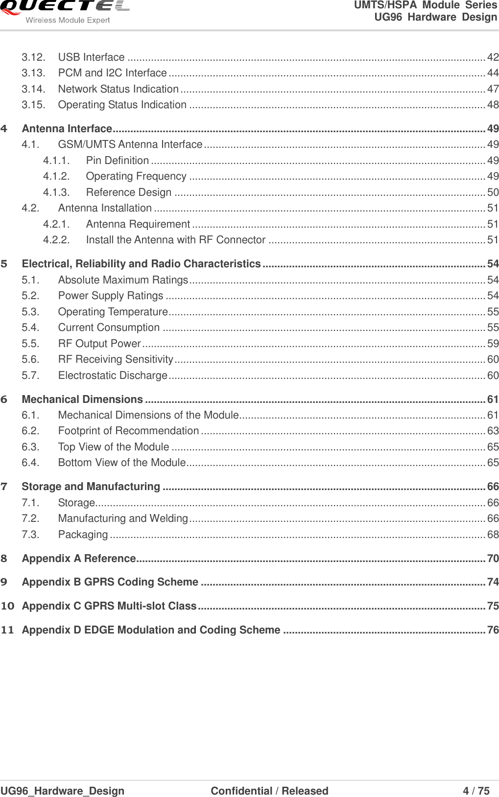
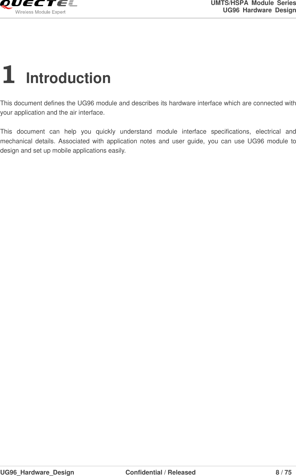
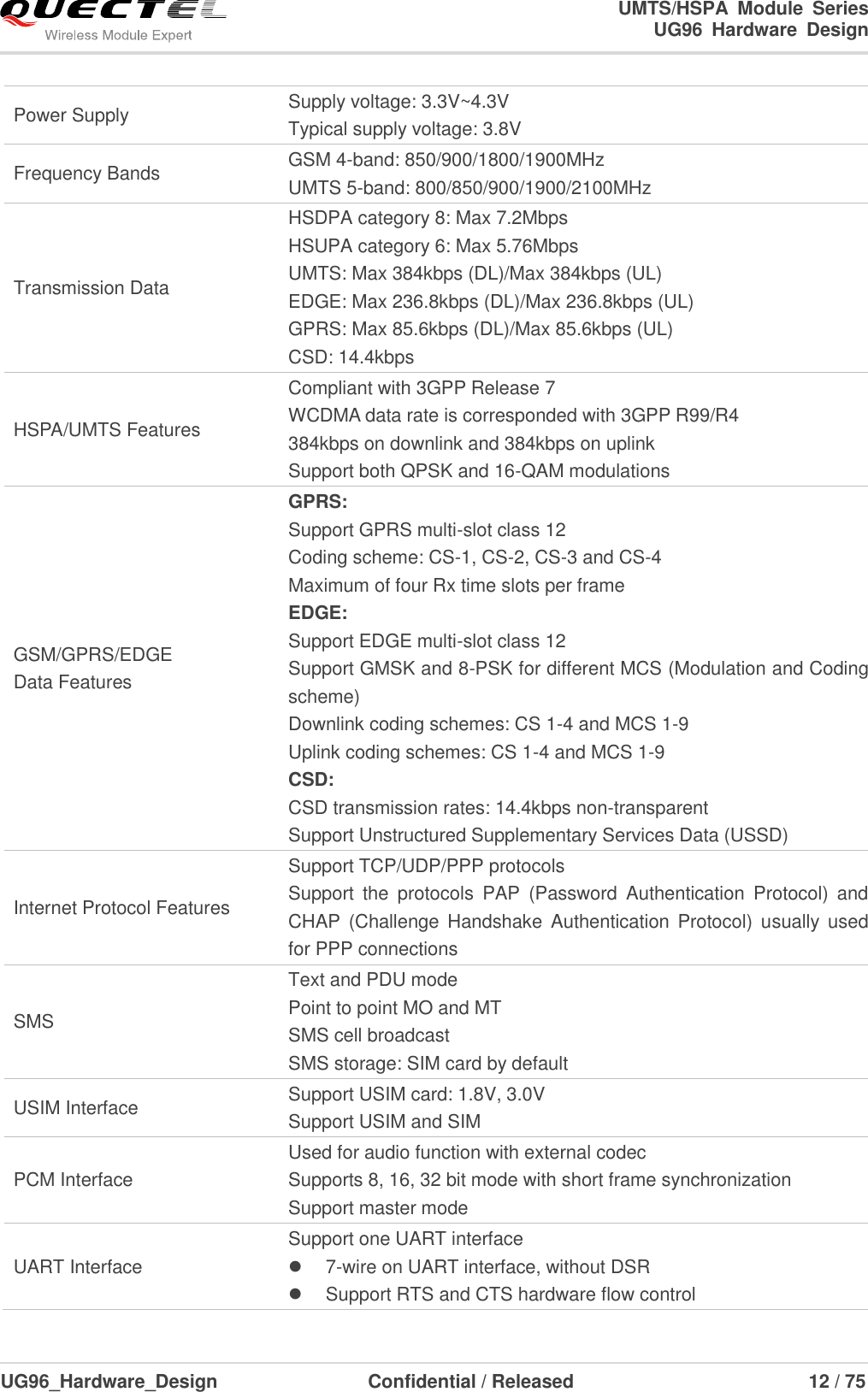
![UMTS/HSPA Module Series UG96 Hardware Design UG96_Hardware_Design Confidential / Released 32 / 75 3.7.2. Turn off Module The following procedures can be used to turn off the module: Normal power down procedure: Turn off the module using command AT+QPOWD. Emergency power down procedure: Turn off the module using the PWRDWN_N pin. Automatic shutdown: Turn off the module automatically if under-voltage or over-voltage is detected. 3.7.2.1. Turn off Module Using AT Command There are several different ways to turn off the module. It is recommended to turn off the module from AT command AT+QPOWD. It is a safe way to turn off the module. This command will let the module log off from the network and allow the firmware to save important data before completely disconnecting the power supply. The power-down scenario is illustrated as the following figure. VBATAT+QPOWDLog off network about 2s to 40sRUNNING Power-down procedure OFFModuleStatusSTATUSRXD Figure 12: Timing of Turning off through AT Command During power-down procedure, module will log off from network and save important data. After logging off, module sends out “OK”, and then sends out “POWERED DOWN” and shuts down the internal power supply. The power on VBAT pins is not allowed to be turned off before the URC “POWERED DOWN” is output to avoid data loss. If logging off is not done within 40s, module will shut down internal power supply forcibly. After that moment, the module enters the power down mode, no other AT commands can be executed, only the RTC is still active. Please refer to document [1] for details about the AT command of AT+QPOWD.](https://usermanual.wiki/Quectel-Wireless-Solutions/201508UG96/User-Guide-2705447-Page-33.png)
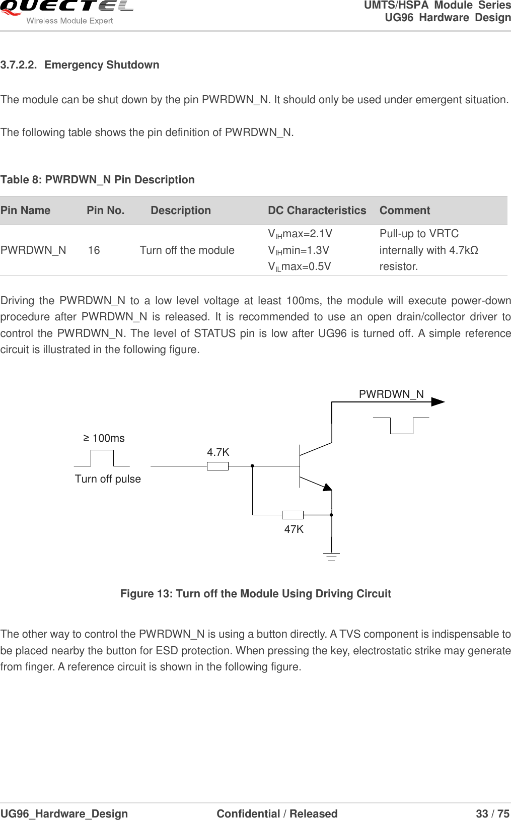
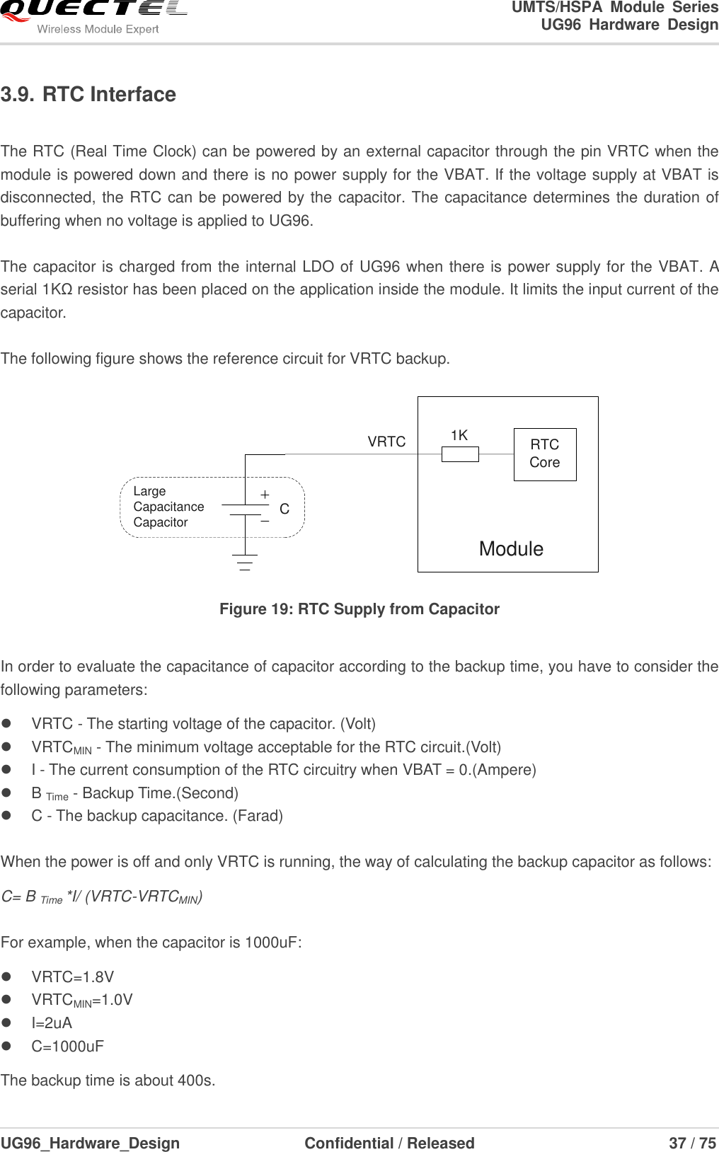
![UMTS/HSPA Module Series UG96 Hardware Design UG96_Hardware_Design Confidential / Released 35 / 75 3.7.2.3. Automatic Shutdown The module will constantly monitor the voltage applied on the VBAT, if the voltage ≤ 3.5V, the following URC will be presented: +QIND: “vbatt”,-1 If the voltage ≥ 4.21V, the following URC will be presented: +QIND: “vbatt”,1 The uncritical voltage is 3.3V to 4.3V, If the voltage > 4.3V or < 3.3V the module would automatically shut down itself. If the voltage < 3.3V, the following URC will be presented: +QIND: “vbatt”,-2 If the voltage > 4.3V, the following URC will be presented: +QIND: “vbatt”,2 The value of voltage threshold can be revised by AT command, refer to document [1] for details. 3.8. Reset the Module The RESET_N can be used to reset the module. Table 9: RESET_N Pin Description Pin Name Pin No. Description DC Characteristics Comment RESET_N 17 Reset the module. VIHmax=2.1V VIHmin=1.3V VILmax=0.5V Pull-up to VRTC internally with 200kΩ resistor. Active low. The module can be reset by driving the RESET_N to a low level voltage for more than 100ms and then releasing. NOTE](https://usermanual.wiki/Quectel-Wireless-Solutions/201508UG96/User-Guide-2705447-Page-36.png)
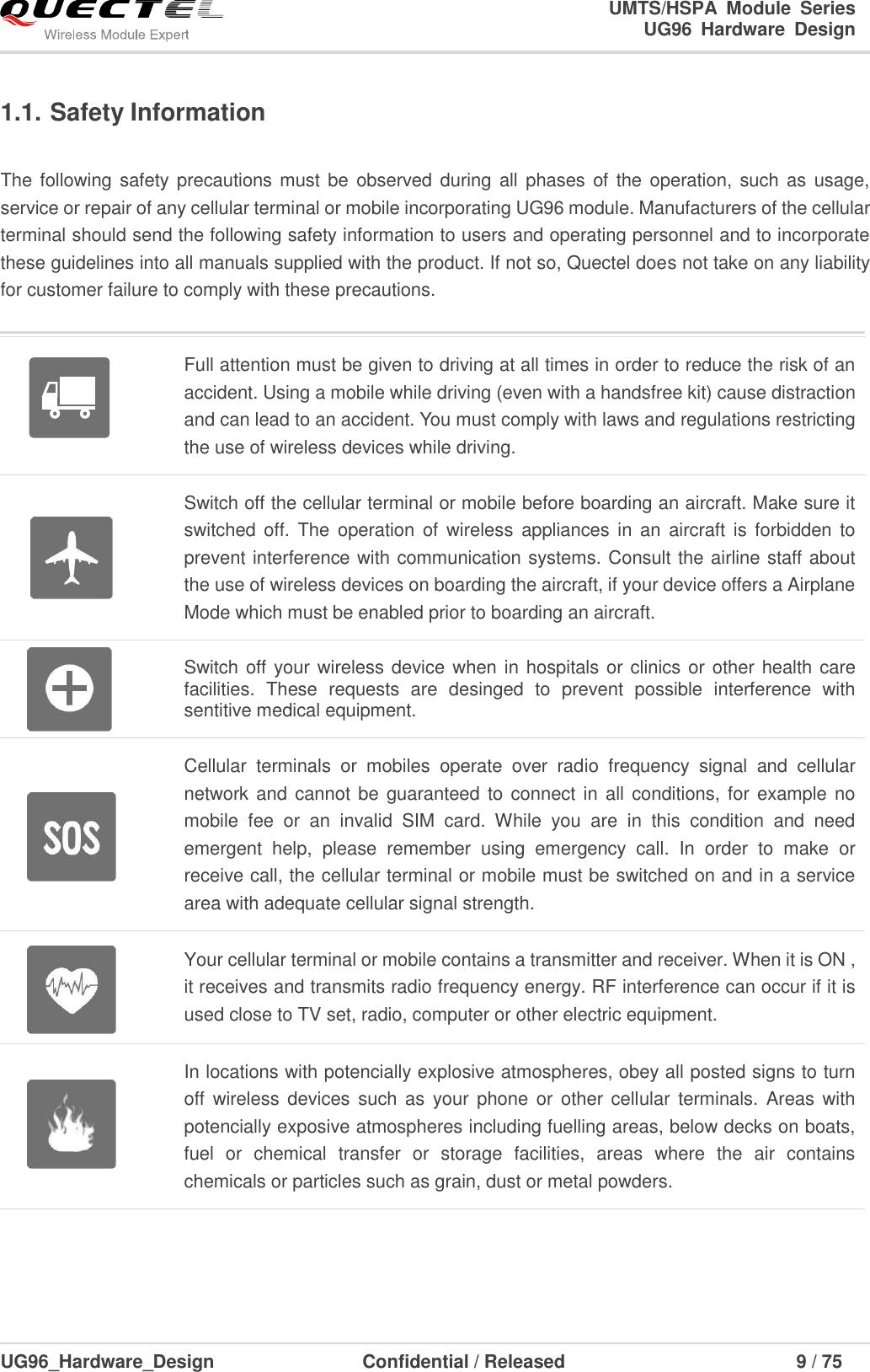
![UMTS/HSPA Module Series UG96 Hardware Design UG96_Hardware_Design Confidential / Released 40 / 75 The following figure is an example of connection between UG96 and PC. A voltage level translator and a RS-232 level translator chip must be inserted between module and PC, since the UART interface does not support the RS-232 level, while supports the 1.8V CMOS level only. TXS0108EPWRDCD_3.3VRTS_3.3VDTR_3.3VRXD_3.3VRI_3.3VCTS_3.3VTXD_3.3VDCDRTSDTRRXDRICTSTXDDCD_1.8VRTS_1.8VDTR_1.8VRXD_1.8VRI_1.8VCTS_1.8VTXD_1.8VVCCAModuleGND GNDVDD_EXT VCCB3.3VDIN1ROUT3ROUT2ROUT1DIN4DIN3DIN2DIN5R1OUTBFORCEON/FORCEOFF /INVALID3.3VDOUT1DOUT2DOUT3DOUT4DOUT5RIN3RIN2RIN1VCC GNDOETranslator DB9MPC sideDCDRTSDTRTXDRICTSRXDDSRGND123456789 Figure 22: RS232 Level Match Circuit 1. The module disables the hardware flow control by default. When hardware flow control is required, RTS and CTS should be connected to the host. AT command AT+IFC=2,2 is used to enable hardware flow control. AT command AT+IFC=0,0 is used to disable the hardware flow control. For more details, please refer to document [1]. 2. Rising edge on DTR will let the module exit from the data mode by default. It can be disabled by AT commands. Refer to document [1] for details. 3. DCD is used as data mode indication. Refer to document [1] for details. 4. It is suggested that you should set USB_DP, USB_DM and USB_VBUS pins as test points and then place these test points on the DTE for debug. 3.11. USIM Card Interface The USIM card interface circuitry meets ETSI and IMT-2000 SIM interface requirements. Both 1.8V and 3.0V USIM cards are supported. NOTES](https://usermanual.wiki/Quectel-Wireless-Solutions/201508UG96/User-Guide-2705447-Page-41.png)
![UMTS/HSPA Module Series UG96 Hardware Design UG96_Hardware_Design Confidential / Released 44 / 75 Keep the ESD components as close as possible to the USB connector. It is suggested that reserve RC circuit near USB connector for debug. The USB interface is recommended to be reserved for firmware upgrade in your design. The following figure shows the recommended test points. ModuleUSB_DMUSB_DPVBAT_BBUSB_VBUSPWRKEYGNDVBAT_RFUSB_DMUSB_DPVBATUSB_VBUSPWRKEYGNDConnector Figure 26: Test Points of Firmware Upgrade 1. UG96 module can only be used as a slave device. 2. It is suggested that you should set USB_DP, USB_DM and USB_VBUS pins as test points and then place these test points on the DTE for debug. 3. USB interface supports software debug and firmware upgrade by default. 3.13. PCM and I2C Interface UG96 provides one Pulse Code Modulation (PCM) digital interface for audio design, which supports the following features: Supports 8, 16, 32 bit mode with short frame synchronization, the PCM support 8 bit mode by default. The PCM codec default configuration is AT+QDAC=1. Refer to document [1] for more details. Supports master mode. Supports audio sample rate 8 kHz. NOTES](https://usermanual.wiki/Quectel-Wireless-Solutions/201508UG96/User-Guide-2705447-Page-45.png)
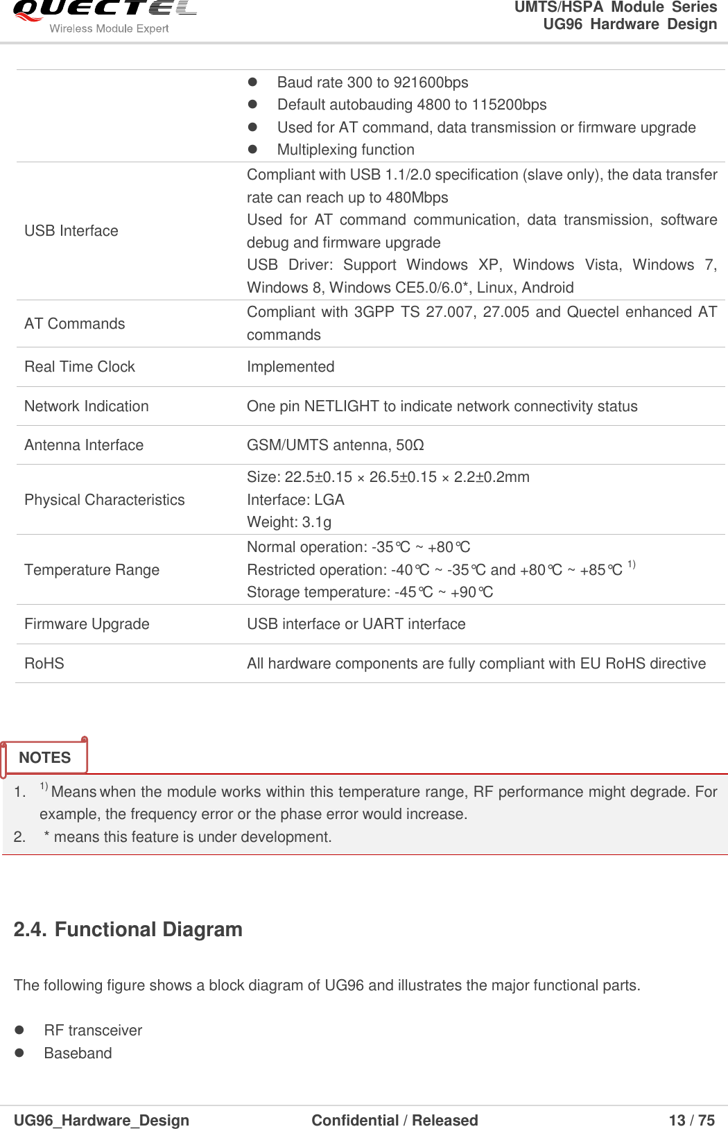
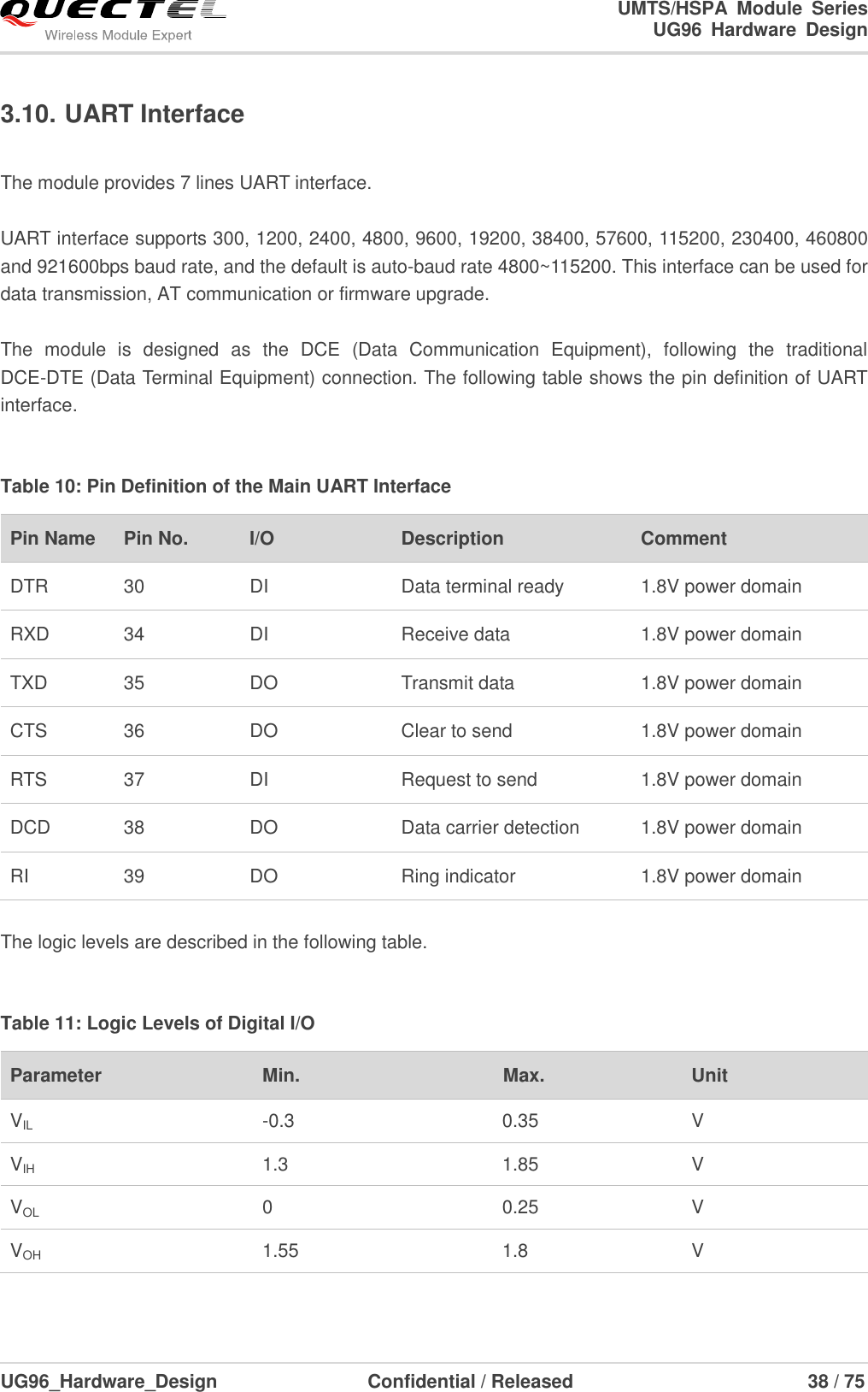
![UMTS/HSPA Module Series UG96 Hardware Design UG96_Hardware_Design Confidential / Released 45 / 75 The following table shows the pin definition of PCM and I2C interface. Table 14: Pin Definition of PCM and I2C Interface Pin Name Pin No. I/O Description Comment PCM_CLK 4 DO PCM data bit clock 1.8V power domain PCM_SYNC 5 DO PCM data frame sync signal 1.8V power domain PCM_IN 6 DI PCM data input 1.8V power domain PCM_OUT 7 DO PCM data output 1.8V power domain I2C_SCL 40 OD I2C serial clock Require external pull-up resistor. I2C_SDA 41 OD I2C serial data Require external pull-up resistor. CLK_OUT 25 DO Clock output Provide a digital clock output for an external audio codec. If unused, keep this pin open. In PCM audio format the MSB of the channel included in the frame (PCM_SYNC) is clocked on the second CLK falling edge after the PCM_SYNC pulse rising edge. The period of the PCM_SYNC signal (frame) lasts for Data word bit +1 clock pulses. UG96’s firmware has integrated the configurations on NAU8814 /ALC5616/MAX9860 application with I2C interface. AT+ADQC command is used to configure the external codec chip linked with PCM interface, and refer to document [1] for more details. Data bit is 32 bit and the sampling rate is 8 KHz. The following figure shows the timing of the application with ALC5616 codec. PCM_CLKPCM_SYNCPCM_IN/OUT32 1 031Sampling freq. = 8 KHz32-bit data wordBCLK = 264 KHz33MSB Figure 27: PCM Master Mode Timing](https://usermanual.wiki/Quectel-Wireless-Solutions/201508UG96/User-Guide-2705447-Page-46.png)
![UMTS/HSPA Module Series UG96 Hardware Design UG96_Hardware_Design Confidential / Released 46 / 75 In general, the BitClockFrequency (BCLK) is calculated by the following expression: BitClockFrequency=(DataWordBit +1) × SamplingFrequency The following figure shows the reference design of PCM interface with external codec IC. PCM_INPCM_OUTPCM_SYNCPCM_CLKI2C_SCLI2C_SDACODECModuleVDD_EXT1K1KBCLKLRCLKDACDATADCDATSCLSDABIASMICBIASMIC+MIC-SPK+SPK-CLK_OUT MCLKRsNM Figure 28: Reference Circuit of PCM Application with Audio Codec 1. It is recommended to reserve RC (e.g. R=22Ω, C=22pF) circuit on the PCM lines, especially for PCM_CLK. 2. UG96 module provides a digital clock output (CLK_OUT) for an external audio codec, the CLK_OUT function is disabled by default. When CLK_OUT is required, AT command is used to provide the codec with a 13/26MHz clock generated from the module. Refer to document [1] for details. If unused, keep this pin open. 3. A RC (e.g. R=22Ω, C=47pF) circuit is recommended to be reserved on CLK_OUT line. If external audio CODEC is MAX9860 or NAU8814, the RC circuit should be mounted, if it is ALC5616, then it is not mounted. NOTES](https://usermanual.wiki/Quectel-Wireless-Solutions/201508UG96/User-Guide-2705447-Page-47.png)
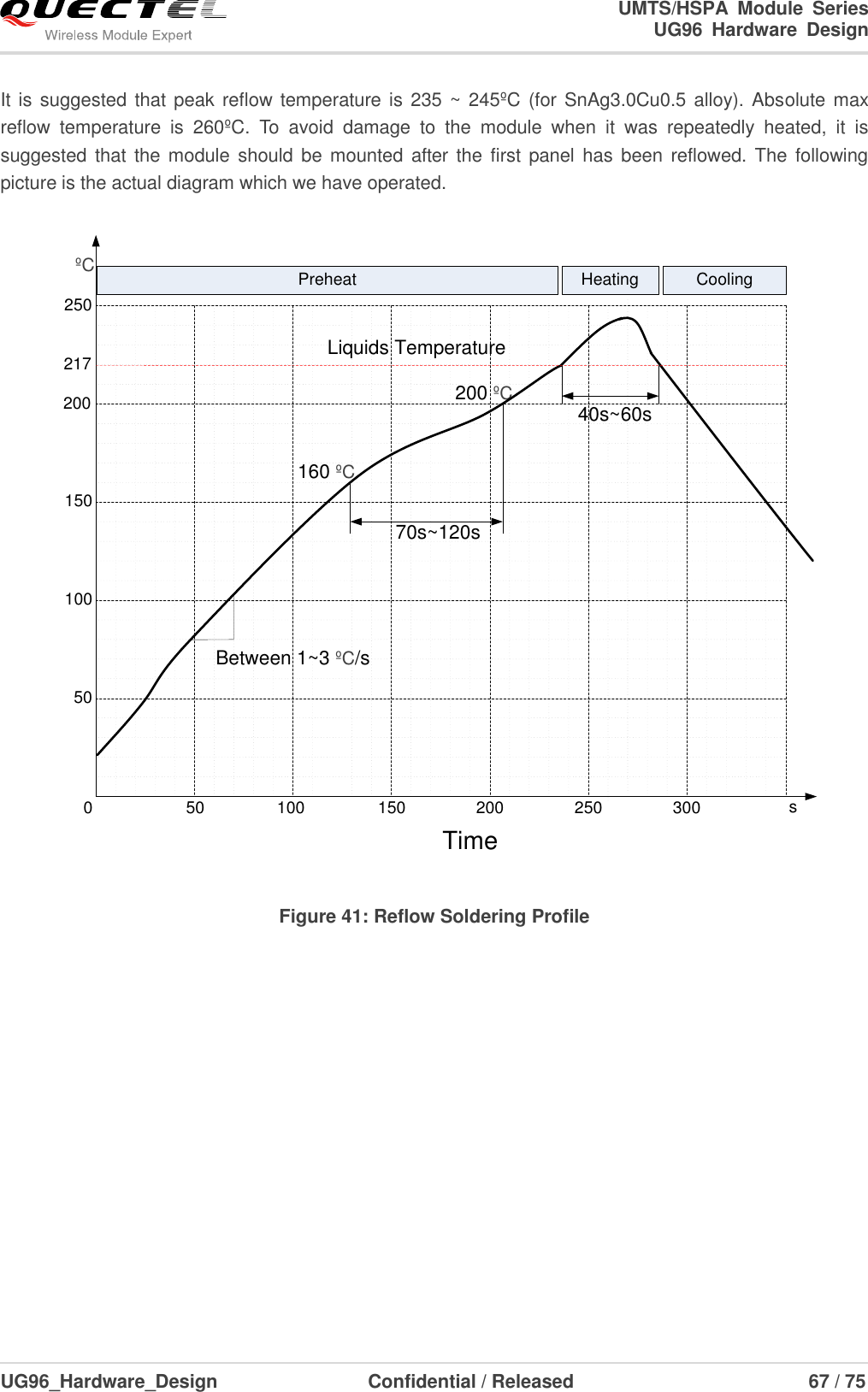
![UMTS/HSPA Module Series UG96 Hardware Design UG96_Hardware_Design Confidential / Released 66 / 75 7 Storage and Manufacturing 7.1. Storage UG96 is stored in the vacuum-sealed bag. The restriction of storage condition is shown as below. Shelf life in sealed bag is 12 months at < 40ºC/90%RH. After this bag is opened, devices that will be subjected to reflow solder or other high temperature process must be: Mounted within 72 hours at factory conditions of ≤ 30ºC/60%RH. Stored at <10% RH. Devices require bake, before mounting, if: Humidity indicator card is >10% when read 23ºC±5ºC. Mounted for more than 72 hours at factory conditions of ≤ 30ºC/60% RH. If baking is required, devices may be baked for 48 hours at 125ºC±5ºC. As plastic container cannot be subjected to high temperature, module needs to be taken out from container to high temperature (125ºC) bake. If shorter bake times are desired, please refer to IPC/JEDECJ-STD-033 for bake procedure. 7.2. Manufacturing and Welding The squeegee should push the paste on the surface of the stencil that makes the paste fill the stencil openings and penetrate to the PCB. The force on the squeegee should be adjusted so as to produce a clean stencil surface on a single pass. To ensure the module soldering quality, the thickness of stencil at the hole of the module pads should be 0.13mm. For details, please refer to document [6]. NOTE](https://usermanual.wiki/Quectel-Wireless-Solutions/201508UG96/User-Guide-2705447-Page-67.png)
![UMTS/HSPA Module Series UG96 Hardware Design UG96_Hardware_Design Confidential / Released 70 / 75 8 Appendix A Reference Table 29: Related Documents SN Document Name Remark [1] Quectel_WCDMA_UGxx_AT_Commands_Manual UGxx AT Commands Manual [2] Quectel_UMTS&LTE_EVB_User_Guide UMTS&LTE EVB User Guide [3] Quectel_UG96_Reference_Design UG96 Reference Design [4] Quectel_UG96&UG95&M95 R2.0_Reference_Design UG96, UG95 and M95 R2.0 Compatible Reference Design [5] Quectel_UG96&UG95&M95 R2.0_Compatible_ Design UG96, UG95 and M95 R2.0 Compatibility Design Specification [6] Quectel_Module_Secondary_SMT_User_Guide Module Secondary SMT User Guide Table 30: Terms and Abbreviations Abbreviation Description AMR Adaptive Multi-rate ARP Antenna Reference Point bps Bits Per Second CHAP Challenge Handshake Authentication Protocol CS Coding Scheme CSD Circuit Switched Data CTS Clear To Send DRX Discontinuous Reception DCE Data Communications Equipment (typically module) DTE Data Terminal Equipment (typically computer, external controller)](https://usermanual.wiki/Quectel-Wireless-Solutions/201508UG96/User-Guide-2705447-Page-71.png)