Quectel Wireless Solutions 201703FC20N WiFi Module User Manual
Quectel Wireless Solutions Company Limited WiFi Module
User Manual


FC20-N Series Hardware Design
FC20-N_Series_Hardware_Design Confidential / Released 1 /
47
Our aim is to provide customers with timely and comprehensive service. For any
assistance, please contact our company headquarters:
Quectel Wireless Solutions Co., Ltd.
Office 501, Building 13, No.99, Tianzhou Road, Shanghai, China, 200233
Tel: +86 21 5108 6236
Email: info@quectel.com
Or our local office. For more information, please visit:
http://www.quectel.com/support/salesupport.aspx
For technical support, or to report documentation errors, please visit:
http://www.quectel.com/support/techsupport.aspx
Or email to: Support@quectel.com
GENERAL NOTES
QUECTEL OFFERS THE INFORMATION AS A SERVICE TO ITS CUSTOMERS. THE INFORMATION
PROVIDED IS BASED UPON CUSTOMERS’ REQUIREMENTS. QUECTEL MAKES EVERY EFFORT
TO ENSURE THE QUALITY OF THE INFORMATION IT MAKES AVAILABLE. QUECTEL DOES NOT
MAKE ANY WARRANTY AS TO THE INFORMATION CONTAINED HEREIN, AND DOES NOT ACCEPT
ANY LIABILITY FOR ANY INJURY, LOSS OR DAMAGE OF ANY KIND INCURRED BY USE OF OR
RELIANCE UPON THE INFORMATION. ALL INFORMATION SUPPLIED HEREIN IS SUBJECT TO
CHANGE WITHOUT PRIOR NOTICE.
COPYRIGHT
THE INFORMATION CONTAINED HERE IS PROPRIETARY TECHNICAL INFORMATION OF
QUECTEL CO., LTD. TRANSMITTING, REPRODUCTION, DISSEMINATION AND EDITING OF THIS
DOCUMENT AS WELL AS UTILIZATION OF THE CONTENT ARE FORBIDDEN WITHOUT
PERMISSION. OFFENDERS WILL BE HELD LIABLE FOR PAYMENT OF DAMAGES. ALL RIGHTS
ARE RESERVED IN THE EVENT OF A PATENT GRANT OR REGISTRATION OF A UTILITY MODEL
OR DESIGN.
Copyright © Quectel Wireless Solutions Co., Ltd. 2016. All rights reserved.

FC20-N Series Hardware Design
FC20-N_Series_Hardware_Design Confidential / Released 2 /
47
About the Document
History
Revision
Date
Author
Description
1.0
2016-11-02
Power JIN
Initial

FC20-N Series Hardware Design
FC20-N_Series_Hardware_Design Confidential / Released 3 /
47
Contents
About the Document ................................................................................................................................... 2
Contents ....................................................................................................................................................... 3
Table Index ................................................................................................................................................... 5
Figure Index ................................................................................................................................................. 6
1 Introduction .......................................................................................................................................... 7
1.1. Safety Information ................................................................................................................... 7
2 Product Concept .................................................................................................................................. 9
2.1. General Description ................................................................................................................. 9
2.2. Directives and Standards ........................................................................................................ 9
2.2.1. FCC Statement ................................................................................................................. 9
2.2.2. FCC Radiation Exposure Statement ................................................................................ 9
2.3. Key Features ......................................................................................................................... 10
2.4. Functional Diagram ............................................................................................................... 11
2.5. Evaluation Board ................................................................................................................... 12
3 Application Interfaces ....................................................................................................................... 13
3.1. General Description ............................................................................................................... 13
3.2. Pin Assignment ...................................................................................................................... 14
3.3. Pin Description ...................................................................................................................... 15
3.4. Power Supply ........................................................................................................................ 18
3.5. WLAN Interface ..................................................................................................................... 20
3.5.1. WAKE_ON_WIRELESS Interface ................................................................................. 21
3.5.2. WLAN_EN ...................................................................................................................... 21
3.5.3. SDIO Interface ............................................................................................................... 21
3.6. Coexistence Interface ............................................................................................................ 23
3.7. Other Interfaces ..................................................................................................................... 23
3.7.1. DBG_TXD Interface ....................................................................................................... 23
3.7.2. 32KHz_IN Interface ........................................................................................................ 24
3.8. Antenna Interface .................................................................................................................. 24
3.8.1. Pin Definition of the RF Antenna .................................................................................... 24
3.8.2. Operating Frequency ..................................................................................................... 25
3.8.3. Reference Design .......................................................................................................... 25
3.8.4. Antenna Requirements .................................................................................................. 25
3.8.5. Install the Antenna with RF Connector .......................................................................... 26
4 Electrical, Reliability and Radio Characteristics ............................................................................ 29
4.1. General Description ............................................................................................................... 29
4.2. Electrical Characteristics ....................................................................................................... 29
4.3. I/O Interface Characteristics .................................................................................................. 30
4.4. Current Consumption ............................................................................................................ 30

FC20-N Series Hardware Design
FC20-N_Series_Hardware_Design Confidential / Released 4 /
47
4.5. RF Performance .................................................................................................................... 32
4.6. Electrostatic Discharge .......................................................................................................... 34
5 Mechanical Dimensions .................................................................................................................... 35
5.1. Mechanical Dimensions of the Module ................................................................................. 35
5.2. Recommended Footprint and Stencil .................................................................................... 37
5.3. Top and Bottom View of the Module ..................................................................................... 39
6 Storage, Manufacturing and Packaging .......................................................................................... 40
6.1. Storage .................................................................................................................................. 40
6.2. Soldering ............................................................................................................................... 41
6.3. Packaging .............................................................................................................................. 42
6.3.1. Tape and Reel Packaging .............................................................................................. 42
7 Appendix A References ..................................................................................................................... 44

FC20-N Series Hardware Design
FC20-N_Series_Hardware_Design Confidential / Released 5 /
47
Table Index
TABLE 1: FC20 SERIES PRODUCTS ................................................................................................................ 7
TABLE 2: KEY FEATURES ............................................................................................................................... 10
TABLE 3: I/O PARAMETERS DEFINITION ....................................................................................................... 15
TABLE 4: PIN DESCRIPTION ........................................................................................................................... 15
TABLE 5: POWER SUPPLY PINS AND GND PINS .......................................................................................... 18
TABLE 6: PIN DEFINITION OF WAKE_ON_WIRELESS ................................................................................. 21
TABLE 7: PIN DEFINITION OF WLAN_EN ....................................................................................................... 21
TABLE 8: PIN DEFINITION OF THE SDIO INTERFACE .................................................................................. 21
TABLE 9: PIN DEFINITION OF COEXISTENCE INTERFACE ......................................................................... 23
TABLE 10: PIN DEFINITION OF DBG_TXD INTERFACE ................................................................................ 24
TABLE 11: PIN DEFINITION OF 32KHZ_IN INTERFACE ................................................................................ 24
TABLE 12: PIN DEFINITION OF THE RF ANTENNA ....................................................................................... 24
TABLE 13: OPERATING FREQUENCY OF THE MODULE ............................................................................. 25
TABLE 14: ANTENNA CABLE REQUIREMENTS ............................................................................................. 26
TABLE 15: ANTENNA REQUIREMENTS .......................................................................................................... 26
TABLE 16: ABSOLUTE MAXIMUM RATINGS .................................................................................................. 29
TABLE 17: RECOMMENDED OPERATING CONDITIONS .............................................................................. 30
TABLE 18: GENERAL DC ELECTRICAL CHARACTERISTICS ....................................................................... 30
TABLE 19: CURRENT CONSUMPTION OF THE MODULE IN LOW POWER MODE .................................... 30
TABLE 20: CURRENT CONSUMPTION OF THE MODULE ............................................................................ 31
TABLE 21: CONDUCTED RF OUTPUT POWER AT 2.4GHZ .......................................................................... 32
TABLE 22: CONDUCTED RF OUTPUT POWER AT 5GHZ ............................................................................. 33
TABLE 23: CONDUCTED RF RECEIVING SENSITIVITY AT 2.4GHZ ............................................................. 33
TABLE 24: CONDUCTED RF RECEIVING SENSITIVITY AT 5GHZ ................................................................ 34
TABLE 25: REEL PACKAGING ......................................................................................................................... 43
TABLE 26: RELATED DOCUMENTS ................................................................................................................ 44
TABLE 27: TERMS AND ABBREVIATIONS ...................................................................................................... 44

FC20-N Series Hardware Design
FC20-N_Series_Hardware_Design Confidential / Released 6 /
47
Figure Index
FIGURE 1: FUNCTIONAL DIAGRAM OF FC20-N MODULE ............................................................................ 11
FIGURE 2: PIN ASSIGNMENT OF FC20 SERIES MODULE ........................................................................... 14
FIGURE 3: REFERENCE CIRCUIT FOR VDD_3V3 ........................................................................................ 19
FIGURE 4: TIMING OF POWER ON/OFF THE FC20 SERIES MODULE ....................................................... 20
FIGURE 5: WLAN INTERFACE CONNECTION ............................................................................................... 20
FIGURE 6: SDIO INTERFACE CONNECTION ................................................................................................. 22
FIGURE 7: COEXISTENCE INTERFACE CONNECTION ................................................................................ 23
FIGURE 8: REFERENCE CIRCUIT FOR RF ANTENNA INTERFACE ............................................................ 25
FIGURE 9: DIMENSIONS OF THE UF.L-R-SMT CONNECTOR (UNIT: MM) .................................................. 26
FIGURE 10: MECHANICALS OF UF.L-LP CONNECTORS (UNIT: MM) .......................................................... 27
FIGURE 11: SPACE FACTOR OF MATED CONNECTOR (UNIT: MM) ............................................................ 27
FIGURE 12: FC20 TOP AND SIDE DIMENSIONS (UNIT: MM) ........................................................................ 35
FIGURE 13: FC20 BOTTOM DIMENSIONS (UNIT: MM) ................................................................................. 36
FIGURE 14: RECOMMENDED FOOTPRINT (UNIT: MM) ................................................................................ 37
FIGURE 15: RECOMMENDED STENCIL (UNIT: MM) ..................................................................................... 38
FIGURE 16: TOP VIEW OF THE MODULE ...................................................................................................... 39
FIGURE 17: BOTTOM VIEW OF THE MODULE .............................................................................................. 39
FIGURE 18: REFLOW SOLDERING THERMAL PROFILE .............................................................................. 41
FIGURE 19: TAPE DIMENSIONS (UNIT: MM) .................................................................................................. 42
FIGURE 20: REEL DIMENSIONS (UNIT: MM) ................................................................................................. 43

FC20-N Series Hardware Design
FC20-N_Series_Hardware_Design Confidential / Released 7 /
47
1 Introduction
This document defines the FC20 series module and describes its hardware interface which is connected
with the customer’s application as well as its air interface.
The document can help customers quickly understand module interface specifications, as well as the
electrical and mechanical details. Associated with application note and user guide, customers can use
FC20 series module to design and set up mobile applications easily.
FC20 series module contains two variants: FC20 and FC20-N. Customers can choose the dedicated type
basing on their requirements. The following table shows the entire models of FC20 series.
Table 1: FC20 Series Products
1.1. Safety Information
The following safety precautions must be observed during all phases of the operation, such as usage,
service or repair of any cellular terminal or mobile incorporating FC20 series module. Manufacturers of
the cellular terminal should send the following safety information to users and operating personnel, and
incorporate these guidelines into all manuals supplied with the product. If not so, Quectel assumes no
liability for the customer’s failure to comply with these precautions.
Full attention must be given to driving at all times in order to reduce the risk of an
accident. Using a mobile while driving (even with a handsfree kit) causes
distraction and can lead to an accident. You must comply with laws and regulations
restricting the use of wireless devices while driving.
Module
Wi-Fi
BT
FC20-N
2.4GHz
Not Supported
FC20-N Series Hardware Design
FC20-N_Series_Hardware_Design Confidential / Released 8 /
47
Switch off the cellular terminal or mobile before boarding an aircraft. Make sure it is
switched off. The operation of wireless appliances in an aircraft is forbidden, so as
to prevent interference with communication systems. Consult the airline staff about
the use of wireless devices on boarding the aircraft, if your device offers an
Airplane Mode which must be enabled prior to boarding an aircraft.
Switch off your wireless device when in hospitals, clinics or other health care
facilities. These requests are desinged to prevent possible interference with
sensitive medical equipment.
Cellular terminals or mobiles operating over radio frequency signal and cellular
network cannot be guaranteed to connect in all conditions, for example no mobile
fee or with an invalid SIM card. While you are in this condition and need emergent
help, please remember using emergency call. In order to make or receive a call,
the cellular terminal or mobile must be switched on and in a service area with
adequate cellular signal strength.
Your cellular terminal or mobile contains a transmitter and receiver. When it is ON,
it receives and transmits radio frequency energy. RF interference can occur if it is
used close to TV set, radio, computer or other electric equipment.
In locations with potentially explosive atmospheres, obey all posted signs to turn
off wireless devices such as your phone or other cellular terminals. Areas with
potentially explosive atmospheres include fuelling areas, below decks on boats,
fuel or chemical transfer or storage facilities, areas where the air contains
chemicals or particles such as grain, dust or metal powders, etc.

FC20-N Series Hardware Design
FC20-N_Series_Hardware_Design Confidential / Released 9 /
47
2 Product Concept
2.1. General Description
FC20-N module is a low-power and low-cost wireless module based on QCA9377-3.
FC20-N module only supports 1×1 IEEE 802.11 b/g/n WLAN standards.
2.2. Directives and Standards
The FC20-N module is designed to comply with the FCC statements. FCC ID: XMR201703FC20N
The Host system using FC20-N should have label “contains FCC ID: XMR201701FC20N
2.2.1. FCC Statement
Changes or modifications not expressly approved by the party responsible for compliance could void the
user’s authority to operate the equipment.
2.2.2. FCC Radiation Exposure Statement
This equipment complies with FCC radiation exposure limits set forth for an uncontrolled environment.
This equipment should be installed and operated with minimum distance 20cm between the radiator and
your body as well as kept minimum 20cm from radio antenna depending on the Mobile status of this
module usage. This module should NOT be installed and operating simultaneously with other radio. The
manual of the host system, which uses FC20-N, must include RF exposure warning statement to advice
user should keep minimum 20cm from the radio antenna of FC20-N module depending on the Mobile
status. Note: If a portable device (such as PDA) uses FC20-N module, the device needs to do permissive
change and SAR testing.
Any Changes or modifications not expressly approved by the party responsible for compliance could void
the user's authority to operate the equipment.
Note: This equipment has been tested and found to comply with the limits for a Class B digital device,
pursuant to part 15 of the FCC Rules. These limits are designed to provide reasonable protection against
harmful interference in a residential installation. This equipment generates uses and can radiate radio
frequency energy and, if not installed and used in accordance with the instructions, may cause harmful

FC20-N Series Hardware Design
FC20-N_Series_Hardware_Design Confidential / Released 10 /
47
interference to radio communications. However, there is no guarantee that interference will not occur in a
particular installation. If this equipment does cause harmful interference to radio or television reception,
which can be determined by turning the equipment off and on, the user is encouraged to try to correct the
interference by one or more of the following measures:
-Reorient or relocate the receiving antenna.
-Increase the separation between theequipment and receiver.
-Connect the equipment into an outlet on a circuit different from that to which the receiver is connected.
-Consult the dealer or an experienced radio/TV technician for help.
2.3. Key Features
The following table describes the detailed features of FC20-N module.
Table 2: Key Features
Features
Implementation
Power Supply
Main supply voltage: 3.3V, 400mA
IO supply voltage: 1.8V
Transmission Data
FC20-N: 802.11b: 1, 2, 5.5, 11Mbps
802.11g: 6, 9, 12, 18, 24, 36, 48, 54Mbps
802.11n: 6.5, 13, 19.5, 26, 39, 52, 58.5, 65Mbps
Transmitting Power
FC20-N: 802.11b/11Mbps: 17dBm
802.11g/54Mbps: 15dBm
802.11n/HT20 MCS7: 14dBm
802.11n/HT40 MCS7: 13dBm
Protocol Features
FC20-N: IEEE 802.11b/g/n
Operator Mode
AP
STA*
Modulation
802.11b: DSSS
802.11g/n20/n40: OFDM
WLAN Interface
SDIO 3.0
Antenna Interface
Wi-Fi antenna, 50Ω
Physical Characteristics
Size: 16.6±0.15 × 13±0.15 × 2.1±0.2mm
Interface: LCC+LGA
Weight: about 0.81g
Temperature Range
Operating temperature range: -35°C~+75°C 1)
Extended temperature range : -40°C~+85°C 2)
FC20-N Series Hardware Design
FC20-N_Series_Hardware_Design Confidential / Released 11 /
47
1. 1) Within operation temperature range, the module is IEEE compliant.
2. 2) Within extended temperature range, the module remains the ability for data transmission. There is
no unrecoverable malfunction. There are also no effects on radio spectrum and no harm to radio
network. Only one or more parameters like Pout might reduce in their value and exceed the specified
tolerances. When the temperature returns to the normal operating temperature levels, the module will
meet IEEE compliant again.
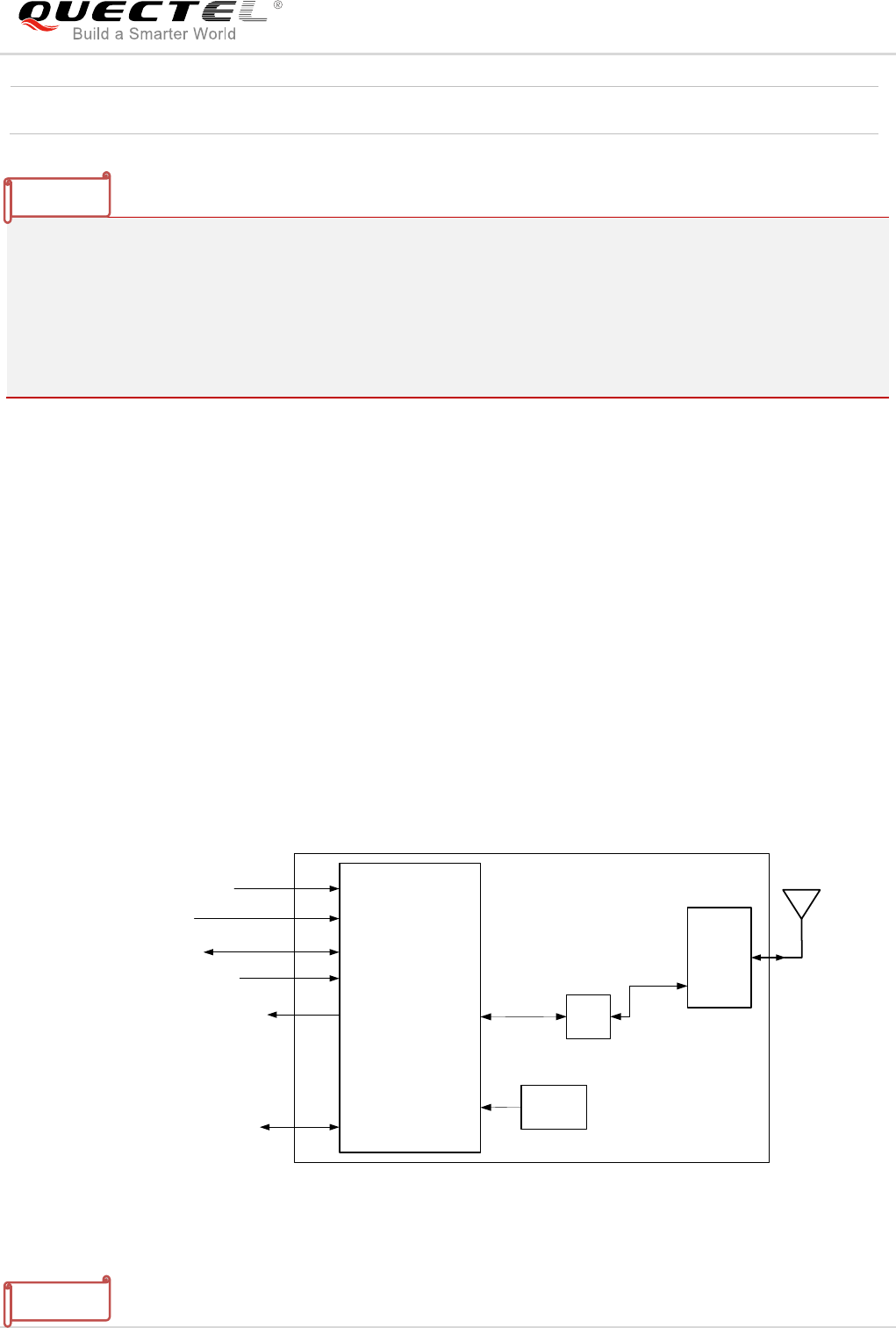
2.4. Functional Diagram
The following figure shows a block diagram of FC20-N module and illustrates the major functional parts.
Power supply
SDIO
PCM and UART
RF antenna
WLAN_EN
RF_ANT
VDD_3V3
VIO
Diplexer
48MHz
XO
TX/RX
SDIO
MAC/BB/Radio 2.4G
Filter
COEX_UART
WAKE_ON_WIRELESS
Figure 1: Functional Diagram of FC20-N Module
RoHS
All hardware components are fully compliant with EU RoHS directive
NOTES
NOTE

FC20-N Series Hardware Design
FC20-N_Series_Hardware_Design Confidential / Released 12 /
47
Please keep these pins open in FC20-N.
2.5. Evaluation Board
In order to help customers to develop applications with FC20-N module, Quectel supplies an evaluation
board (EVB), a RS-232 to USB cable, a USB data cable, a power adapter, 4 antennas and other
peripherals to control or test the module. For details, please refer to document [1].

FC20-N Series Hardware Design
FC20-N_Series_Hardware_Design Confidential / Released 13 /
47
3 Application Interfaces
3.1. General Description
FC20-N module is equipped with 38 LCC pads and 14 LGA pads that can be connected to the cellular
application platform. Sub-interfaces included in these pads are described in details in following chapters:
Power supply
WLAN interface
Coexistence interface
Antenna interface
FC20-N Series Hardware Design
FC20-N_Series_Hardware_Design Confidential / Released 14 /
47
3.2. Pin Assignment
32
34
35
33
36
37
38
29
28
30
31
27
26
24
23
25
22
21
20
19
17
16
18
15
14
13
47
48
49
46
WLAN_EN
GND
RF_ANT
GND
GND
SDIO_CMD
SDIO_CLK
SDIO_D0
SDIO_D1
SDIO_D2
SDIO_D3
VDD_3V3
GND
GND
RESERVED
DBG_TXD
BT_UART_CTS
BT_EN
VIO
RESERVED
GND Pins
LTE_UART_TXD
LTE_UART_RXD
BT_UART_RTS
3
4
2
1
5
6
8
9
7
10
11
12
51 50
52
40
39
41
42
44 4543
PCM_IN
PCM_SYNC
PCM_CLK
PCM_OUT
BT_UART_TXD
BT_UART_RXD
32KHz_IN
GND
GND
RESERVED
RESERVED
RESERVED
RESERVED
WAKE_ON_WIRELESS
Power Pins
GND
Signal Pins Reserved Pins
Figure 2: Pin Assignment of FC20 Series Module
Please keep all RESERVED pins open.
NOTE

FC20-N Series Hardware Design
FC20-N_Series_Hardware_Design Confidential / Released 15 /
47
3.3. Pin Description
The following tables show the pin definition of FC20 series.
Table 3: I/O Parameters Definition
Type
Description
IO
Bidirectional input/output
DI
Digital input
DO
Digital output
PI
Power input
Table 4: Pin Description
Power Supply
Pin Name
Pin No.
I/O
Description
DC Characteristics
Comment
VDD_3V3
21
PI
Main power supply
for module
Vmax=3.46V
Vmin=3.14V
Vnorm=3.3V
It must be able to
provide sufficient
current up to 0.9A.
VIO
11
PI
Power supply for
module IO pin
Vmax=1.89V
Vmin=1.71V
Vnorm=1.8V
It is powered by EC20
R2.0/EC21/EC25
module.
GND
1, 12, 20,
28, 29,
31, 36,
38~40,
43~45,
48~52
Ground
WLAN Interface
Pin Name
Pin No.
I/O
Description
DC Characteristics
Comment
WAKE_ON_
WIRELESS
32
DO
Wake up host
VOLmax=0.18V
VOHmin=1.62V
1.8V power domain.
Active low.
If unused, keep this
pin open.
WLAN_EN
9
DI
WLAN enabled
VILmin=-0.3V
VILmax=0.54V
1.8V power domain.
Active high.

FC20-N Series Hardware Design
FC20-N_Series_Hardware_Design Confidential / Released 16 /
47
VIHmin=1.26V
VIHmax=2.0V
SDIO_D3
22
IO
SDIO data pin bit 3
VOLmax=0.18V
VOHmin=1.62V
VILmin=-0.3V
VILmax=0.54V
VIHmin=1.26V
VIHmax=2.0V
1.8V power domain
SDIO_D2
23
IO
SDIO data pin bit 2
VOLmax=0.18V
VOHmin=1.62V
VILmin=-0.3V
VILmax=0.54V
VIHmin=1.26V
VIHmax=2.0V
1.8V power domain.
Require external
pull-up to 1.8V.
SDIO_D1
24
IO
SDIO data pin bit 1
VOLmax=0.18V
VOHmin=1.62V
VILmin=-0.3V
VILmax=0.54V
VIHmin=1.26V
VIHmax=2.0V
1.8V power domain
SDIO_D0
25
IO
SDIO data pin bit 0
VOLmax=0.18V
VOHmin=1.62V
VILmin=-0.3V
VILmax=0.54V
VIHmin=1.26V
VIHmax=2.0V
1.8V power domain
SDIO_CLK
26
DI
SDIO clock
VILmin=-0.3V
VILmax=0.54V
VIHmin=1.26V
VIHmax=2.0V
1.8V power domain
SDIO_CMD
27
IO
SDIO command
VOLmax=0.18V
VOHmin=1.62V
VILmin=-0.3V
VILmax=0.54V
VIHmin=1.26V
VIHmax=2.0V
1.8V power domain
BT Interface
Pin Name
Pin No.
I/O
Description
DC Characteristics
Comment
BT_EN
10
DI
Bluetooth enabled
VILmin=-0.3V
VILmax=0.54V
VIHmin=1.26V
VIHmax=2.0V
1.8V power domain.
Active high.

FC20-N Series Hardware Design
FC20-N_Series_Hardware_Design Confidential / Released 17 /
47
PCM_IN
13
DI
Bluetooth PCM data
input
VILmin=-0.3V
VILmax=0.54V
VIHmin=1.26V
VIHmax=2.0V
1.8V power domain.
If unused, keep this
pin open.
PCM_SYNC
14
DI
Bluetooth PCM data
frame sync signal
VILmin=-0.3V
VILmax=0.54V
VIHmin=1.26V
VIHmax=2.0V
1.8V power domain.
If unused, keep this
pin open.
PCM_CLK
15
DI
Bluetooth PCM clock
VILmin=-0.3V
VILmax=0.54V
VIHmin=1.26V
VIHmax=2.0V
1.8V power domain.
If unused, keep this
pin open.
PCM_OUT
16
DO
Bluetooth PCM data
output
VOLmax=0.18V
VOHmin=1.62V
1.8V power domain.
If unused, keep this
pin open.
BT_UART_
RTS
7
DO
Request to send
VOLmax=0.18V
VOHmin=1.62V
1.8V power domain.
If unused, keep this
pin open.
BT_UART_
CTS
8
DI
Clear to send
VILmin=-0.3V
VILmax=0.54V
VIHmin=1.26V
VIHmax=2.0V
1.8V power domain.
If unused, keep this
pin open.
BT_UART_
TXD
17
DO
Bluetooth transmits
data
VOLmax=0.18V
VOHmin=1.62V
1.8V power domain.
If unused, keep this
pin open.
BT_UART_
RXD
18
DI
Bluetooth receives
data
VILmin=-0.3V
VILmax=0.54V
VIHmin=1.26V
VIHmax=2.0V
1.8V power domain.
If unused, keep this
pin open.
Coexistence Interface
Pin Name
Pin No.
I/O
Description
DC Characteristics
Comment
LTE_UART_
TXD
5
DO
LTE coexistence
signal
VOLmax=0.18V
VOHmin=1.62V
1.8V power domain.
If unused, keep this
pin open.
LTE_UART_
RXD
6
DI
LTE coexistence
signal
VILmin=-0.3V
VILmax=0.54V
VIHmin=1.26V
VIHmax=2.0V
1.8V power domain.
If unused, keep this
pin open.
RF Interface
Pin Name
Pin No.
I/O
Description
DC Characteristics
Comment
FC20-N Series Hardware Design
FC20-N_Series_Hardware_Design Confidential / Released 18 /
47
RF_ANT
30
IO
WLAN and BT
antenna
50Ω impedance.
Other Pins
Pin Name
Pin No.
I/O
Description
DC Characteristics
Comment
DBG_TXD
4
DO
Software debugging
VOLmax=0.18V
VOHmin=1.62V
1.8V power domain.
If unused, keep this pin
open.
32KHz_IN
19
DI
Low power.
External 32.768KHz
clock input is
required in sleep
mode.
VILmin=-0.3V
VILmax=0.54V
VIHmin=1.26V
VIHmax=2.0V
1.8V power domain.
If unused, keep this pin
open.
RESERVED Pins
Pin Name
Pin No.
I/O
Description
DC Characteristics
Comment
RESERVED
2, 3,
33~35,
37, 41,
42, 46, 47
Reserved
Keep these pins
unconnected.
FC20-N module does not support BT interface and coexistence interface.
3.4. Power Supply
The following table shows the power supply pins and the ground pins of FC20 series. The VIO is powered
by EC20 R2.0/EC21/EC25.
Table 5: Power Supply Pins and GND Pins
Pin Name
Pin No.
Description
Min.
Typ.
Max.
Unit
VDD_3V3
21
Main power supply for module
3.14
3.3
3.46
V
VIO
11
Power supply for module IO
1.71
1.8
1.89
V
GND
1, 12, 20,
Ground
NOTE
FC20-N Series Hardware Design
FC20-N_Series_Hardware_Design Confidential / Released 19 /
47
28, 29, 31,
36, 38~40,
43~45,
48~52
FC20 series is powered by VDD_3V3, and it is recommended to use power supply chip whose maximum
output current is more than 1.2A.
The following figure shows a reference design for VDD_3V3, which is controlled by PM_ENABLE. And
PM_ENABLE should be connected to pin 127 of EC20 R2.0/EC21/EC25. For more details, please refer to
document [2], [3] or [4].
TPS630242
L1
L1
L2
L2
VIN
VIN
VIN
VINA
GND
EN
VOUT
VOUT
VOUT
PFM/PWM
FB
PGND
D2
D3
E1
E2
E3
E4
C4
D1 B1
A1
L1 L2
PGND
PGND
U402
D4
B2
B3
A2
A3
A4
B4
C1
C2
C3
C406
R408
C405
10uF
1M
L401
1uH
R407
100K
22uF
C407
22uF
PM_ENABLE
DC_5V
DC_5V
VDD_3V3
Figure 3: Reference Circuit for VDD_3V3
FC20-N Series Hardware Design
FC20-N_Series_Hardware_Design Confidential / Released 20 /
47
The following figure shows the recommended power on/off sequences for FC20 series.
VDD_3V3
≥ 5us
Module
Status Runnig
WLAN_EN
Power up Power down
TBD
PM_ENABLE
>0 > 0
VIO
BT_EN
Figure 4: Timing of Power ON/OFF the FC20 Series Module
Execute AT command AT+QWIFI=1 to open VDD_3V3 and WLAN.
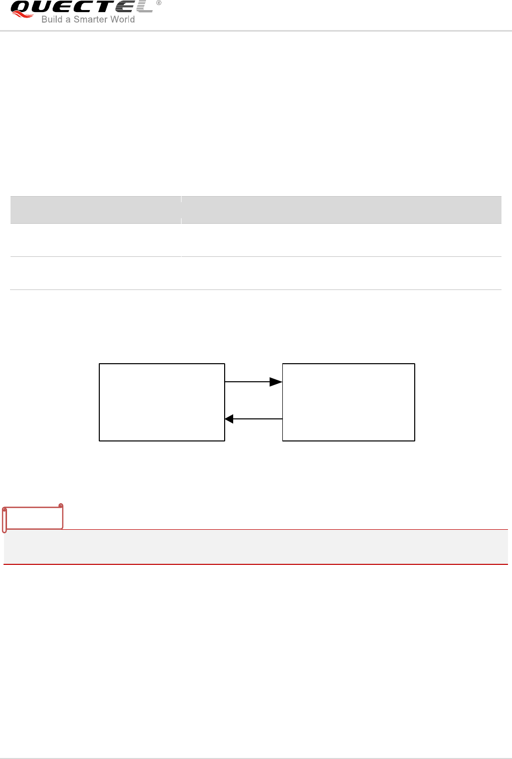
3.5. WLAN Interface
The following figure shows the WLAN interface connection between FC20 series and EC20
R2.0/EC21/EC25.
EC20 R2.0/
EC21/EC25
FC20 Series
SDIO
WLAN_ENWLAN_EN
WAKE_ON_WIRELESS
WAKE_ON_WIRELESS
SDIO
Figure 5: WLAN Interface Connection
FC20-N Series Hardware Design
FC20-N_Series_Hardware_Design Confidential / Released 21 /
47
3.5.1. WAKE_ON_WIRELESS Interface
WAKE_ON_WIRELESS interface is used to wake up the EC20 R2.0/EC21/EC25. When
WAKE_ON_WIRELESS is pulled down, EC20 R2.0/EC21/EC25 can be woken up.
Table 6: Pin Definition of WAKE_ON_WIRELESS
Pin Name
Pin No.
I/O
Description
Comment
WAKE_ON_WIRELESS
32
DO
Wake up host
Active low.
If unused, keep this pin
open.
3.5.2. WLAN_EN
WLAN_EN is used to control the WLAN function of FC20 series. When WLAN_EN is at high level voltage,
WLAN function will be enabled.
Table 7: Pin Definition of WLAN_EN
Pin Name
Pin No.
I/O
Description
Comment
WLAN_EN
9
DI
WLAN enabled
Active high
WLAN_EN is a sensitive signal, which should be guarded by ground and routed as close as possible to
FC20 series module.
3.5.3. SDIO Interface
The following table shows the pin definition of the SDIO interface of FC20 series.
Table 8: Pin Definition of the SDIO Interface
Pin Name
Pin No.
I/O
Description
Comment
SDIO_D3
22
IO
SDIO data pin bit 3
1.8V power domain
SDIO_D2
23
IO
SDIO data pin bit 2
1.8V power domain.
Require external pull-up to
NOTE
FC20-N Series Hardware Design
FC20-N_Series_Hardware_Design Confidential / Released 22 /
47
1.8V.
SDIO_D1
24
IO
SDIO data pin bit 1
1.8V power domain
SDIO_D0
25
IO
SDIO data pin bit 0
1.8V power domain
SDIO_CLK
26
DI
SDIO clock
1.8V power domain
SDIO_CMD
27
IO
SDIO command
1.8V power domain
The following figure shows the SDIO interface connection between FC20 series and EC20
R2.0/EC21/EC25.
SDIO_CLK
SDIO_CMD
SDIO_D0
SDIO_D1
SDIO_D2
SDIO_D3
EC20 R2.0/
EC21/EC25
FC20 Series
SD1_D0
SD1_D1
SD1_D2
SD1_D3
SD1_CLK
SD1_CMD
10K
NM_10K
VIO VIO VIO VIO VIO VIO
NM_10K
NM_10K
NM_10K
NM_10K
NM_10nF
Figure 6: SDIO Interface Connection
In order to ensure the performance of SDIO, please comply with the following principles:
SDIO signals are very high-speed signals. Please prevent crosstalk between them and other
sensitive signals.
Keep SDIO traces as parallel as possible in the same layer. Make sure SDIO lines are guarded by
ground vias and not crossed.
Do not route SDIO signal traces under crystals, oscillators, magnetic devices and RF signal traces.
The pull-up resistor on SDIO_D2 line must be mounted.
Keep SDIO traces as short as possible with equal length, and impedance control as 50Ω.
The spacing to all other signals is greater than 2 times of the line width.
FC20-N Series Hardware Design
FC20-N_Series_Hardware_Design Confidential / Released 23 /
47
3.6. Coexistence Interface
Coexistence function is only supported by FC20. Please keep these pins open in FC20-N.
The following table shows the pin definition of FC20’s coexistence interface.
Table 9: Pin Definition of Coexistence Interface
Pin Name
Pin No.
I/O
Description
Comment
LTE_UART_TXD
5
DO
LTE coexistence signal
If unused, keep this pin
open.
LTE_UART_RXD
6
DI
LTE coexistence signal
If unused, keep this pin
open.
FC20 module supports LTE-WLAN coexistence and LTE-BT coexistence. The following figure shows
the coexistence interface connection between FC20 and EC20 R2.0/EC21/EC25.
LTE_UART_RXD
LTE_UART_TXD
FC20
COEX_UART_RX
COEX_UART_TX
EC2 R2.0/
EC21/EC25
Figure 7: Coexistence Interface Connection
LTE-BT coexistence function is under development.
3.7. Other Interfaces
3.7.1. DBG_TXD Interface
DBG_TXD interface can be used for log output.
NOTE

FC20-N Series Hardware Design
FC20-N_Series_Hardware_Design Confidential / Released 24 /
47
Table 10: Pin Definition of DBG_TXD Interface
Pin Name
Pin No.
I/O
Description
Comment
DBG_TXD
4
DO
Software debugging
If unused, keep this pin
open.
3.7.2. 32KHz_IN Interface
The 32KHz clock is used in low power mode such as IEEE power saving mode and sleep mode. It serves
as a timer to determine when to wake up FC20 series module to receive beacons in various power saving
schemes, and to maintain basic logic operations when in sleep mode. The sleep clock signal is
transferred from EC20 R2.0/EC21/EC25 module.
Table 11: Pin Definition of 32KHz_IN Interface
Pin Name
Pin No.
I/O
Description
Comment
32KHz_IN
19
DI
Low power.
External 32.768KHz
clock input is required
in sleep mode.
If unused, keep this pin
open.
3.8. Antenna Interface
The pin 30 is the RF antenna pad. And the RF interface has an impedance of 50Ω.
3.8.1. Pin Definition of the RF Antenna
Table 12: Pin Definition of the RF Antenna
Pin Name
Pin No.
I/O
Description
Comment
GND
28
Ground
GND
29
Ground
FC20-N Series Hardware Design
FC20-N_Series_Hardware_Design Confidential / Released 25 /
47
RF_ANT
30
IO
RF antenna pad
50Ω impedance
GND
31
Ground
3.8.2. Operating Frequency
Table 13: Operating Frequency of the Module
Feature
Frequency
Unit
WLAN-2.4GHz
2.412~2.462
GHz
3.8.3. Reference Design
FC20 series module provides an RF antenna pad for antenna connection. The RF trace in host PCB
connected to the module’s RF antenna pad should be microstrip line or other types of RF trace, whose
characteristic impendence should be close to 50Ω. FC20 series module comes with grounding pads
which are next to the antenna pad in order to give a better grounding.
The RF external circuit is recommended as following figure. And a π-type matching circuit should be
reserved for better RF performance. The capacitors are not mounted by default.
RF_ANT R1
C1
NM
C2
NM
FC20 Series
0R
Figure 8: Reference Circuit for RF Antenna Interface
3.8.4. Antenna Requirements
The following table shows the requirements on RF antenna.
FC20-N Series Hardware Design
FC20-N_Series_Hardware_Design Confidential / Released 26 /
47
Table 14: Antenna Cable Requirements
Type
Requirements
2.412~2.462GHz
Cable insertion loss <1dB
Table 15: Antenna Requirements
Type
Requirements
Frequency Range
2.412~2.462GHz
VSWR
<2:1 recommended
Gain (dBi)
1 typical
Max Input Power (W)
50
Input Impedance (Ω)
50
Polarization Type
Vertical
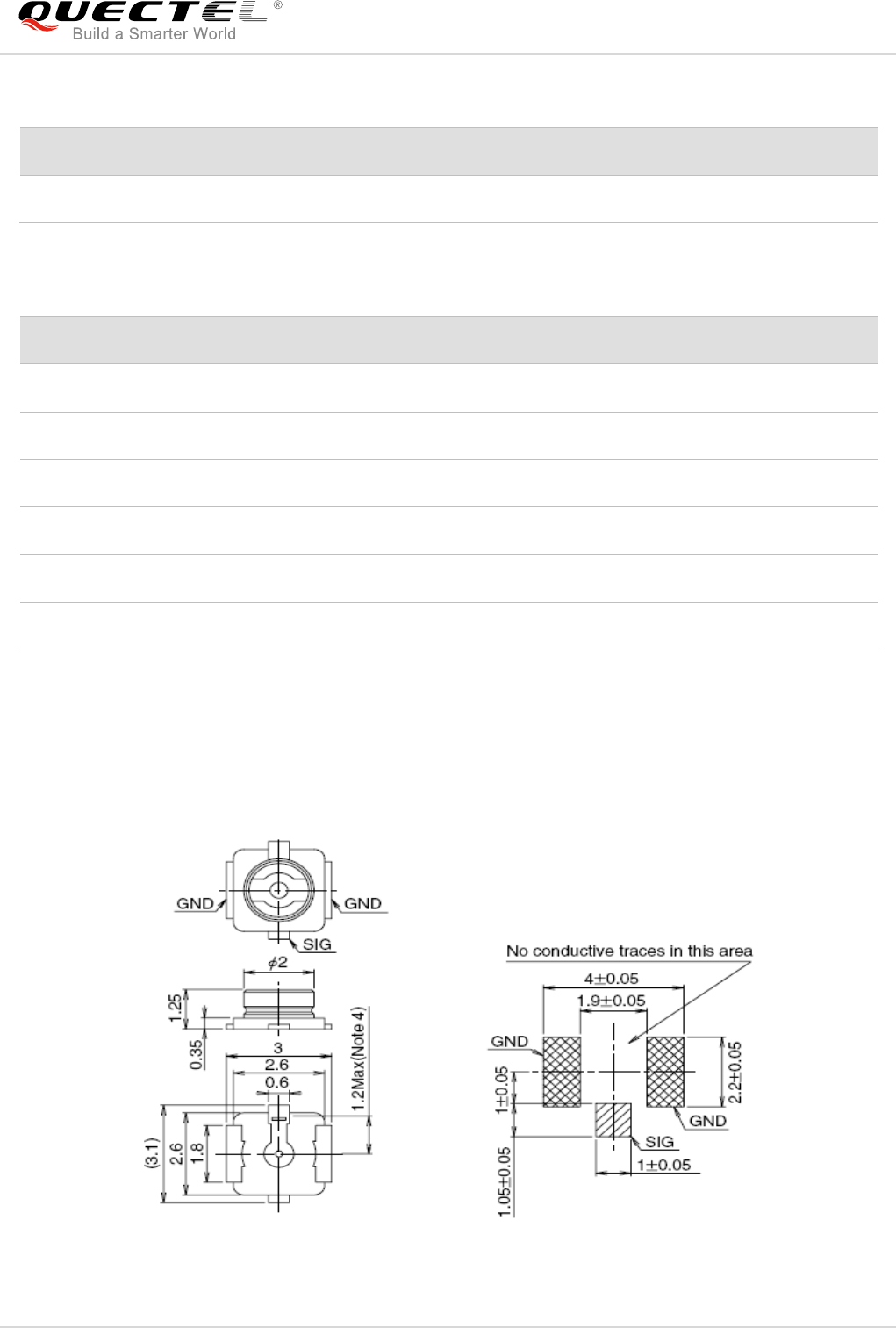
3.8.5. Install the Antenna with RF Connector
The following figure is the antenna installation with RF connector provided by HIROSE. The
recommended RF connector is UF.L-R-SMT.
Figure 9: Dimensions of the UF.L-R-SMT Connector (Unit: mm)
FC20-N Series Hardware Design
FC20-N_Series_Hardware_Design Confidential / Released 27 /
47
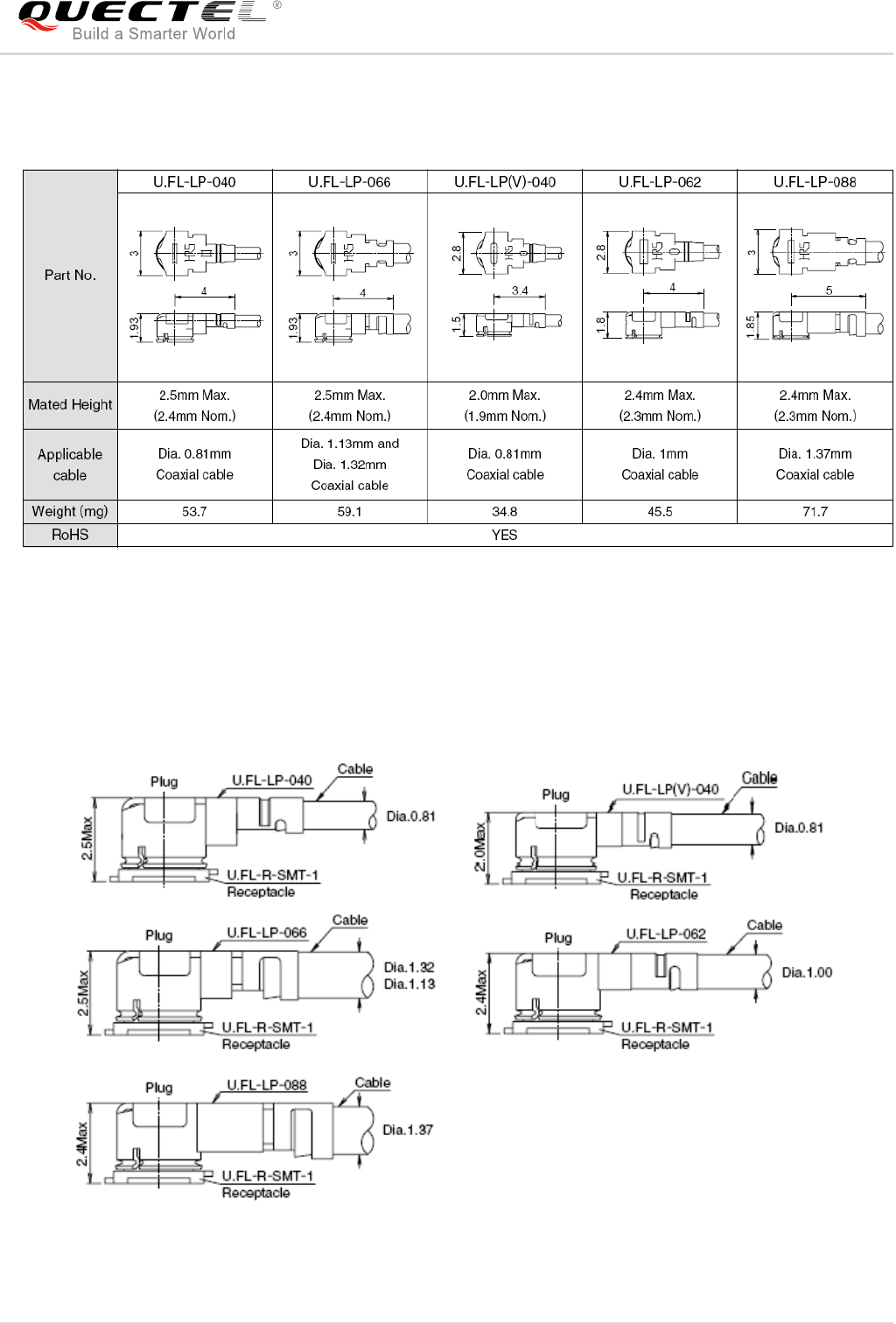
Customers can use U.FL-LP serial connector listed in the following figure to match the UF.L-R-SMT.
Figure 10: Mechanicals of UF.L-LP Connectors (Unit: mm)
The following figure describes the space factor of mated connector
Figure 11: Space Factor of Mated Connector (Unit: mm)


FC20-N Series Hardware Design
FC20-N_Series_Hardware_Design Confidential / Released 29 /
47
4 Electrical, Reliability and Radio
Characteristics
4.1. General Description
This chapter mainly introduces the electrical and the radio frequency characteristics of FC20 series
module, which are listed in detail in the following chapters:
Electrical characteristics
I/O interface characteristics
Current consumption
RF performance
Electrostatic discharge
4.2. Electrical Characteristics
The following table shows the absolute maximum ratings.
Table 16: Absolute Maximum Ratings
Parameter
Min.
Max.
Unit
VDD_3V3
-0.3
4.0
V
VIO
-0.3
1.89
V
Digital I/O input voltage
-0.3
VIO+0.2
V

FC20-N Series Hardware Design
FC20-N_Series_Hardware_Design Confidential / Released 30 /
47
The following table shows the recommended operating conditions for FC20 series module.
Table 17: Recommended Operating Conditions
Parameter
Min.
Typ.
Max.
Unit
VDD_3V3
3.14
3.3
3.46
V
VIO
1.71
1.8
1.89
V
4.3. I/O Interface Characteristics
The following table shows the general DC electrical characteristics over recommended operating
conditions (unless otherwise specified).
Table 18: General DC Electrical Characteristics
Symbol
Parameter
Min.
Max.
Unit
VIH
High Level Input Voltage
0.7*VIO
VIO+0.2
V
VIL
Low Level Input Voltage
-0.3
0.3*VIO
V
VOH
High Level Output Voltage
0.9*VIO
VIO
V
VOL
Low Level Output Voltage
0
0.1*VIO
V
IIL
Input Leakage Current
-5
5
uA
4.4. Current Consumption
The values of current consumption are shown as below.
Table 19: Current Consumption of the Module in Low Power Mode
Description
Conditions
IWLAN_3V3
IVIO
Unit
OFF State
AT+QWIFI=0
0
554
uA

FC20-N Series Hardware Design
FC20-N_Series_Hardware_Design Confidential / Released 31 /
47
Description
Conditions
IWLAN_3V3
IVIO
Unit
Idle
AT+QWIFI=1
66
6.5
mA
Table 20: Current Consumption of the Module
Description
Conditions
IWLAN_3V3
Unit
802.11b
TX 1Mbps @17.5dBm
370
mA
TX 11Mbps @17.2dBm
357
mA
RX 1Mbps
48
mA
RX 11Mbps
49
mA
802.11g
TX 6Mbps @16dBm
328
mA
TX 54Mbps @14.8dBm
245
mA
RX 6Mbps
49
mA
RX 54Mbps
50
mA
802.11n
TX HT20-MCS0 @15.8dBm
322
mA
TX HT20-MCS7 @13.5dBm
234
mA
TX HT40-MCS0 @14.5dBm
291
mA
TX HT40-MCS7 @12.5dBm
194
mA
RX HT20-MCS0
49
mA
RX HT20-MCS7
50
mA
RX HT40-MCS0
54
mA
RX HT40-MCS7
52
mA
802.11a
TX HT20 MCS0 @dBm
TBD
mA
TX HT20 MCS7 @dBm
TBD
mA
RX HT20 MCS0
TBD
mA
RX HT20 MCS7
TBD
mA
FC20-N Series Hardware Design
FC20-N_Series_Hardware_Design Confidential / Released 32 /
47
Description
Conditions
IWLAN_3V3
Unit
TX VHT20 MCS0 @13.2dBm
378
mA
802.11ac
TX VHT20 MCS8 @12.5dBm
289
mA
TX VHT40 MCS0 @13.5dBm
372
mA
TX VHT40 MCS9 @10.5dBm
244
mA
TX VHT80 MCS0 @13dBm
355
mA
TX VHT80 MCS9 @10dBm
220
mA
RX VHT20 MCS0
78
mA
RX VHT20 MCS8
78
mA
RX VHT40 MCS0
85
mA
RX VHT40 MCS9
84
mA
RX VHT80 MCS8
92
mA
RX VHT80 MCS9
91
mA
OFF state: Execute AT+QWIFI=0 to bring the module to this state. Under the state, the sleep clock is
disabled and no data is saved.
4.5. RF Performance
The following tables summarize the transmitter and receiver characteristics of FC20 series.
Table 21: Conducted RF Output Power at 2.4GHz
Frequency
Min.
Typ.
Unit
802.11b @1Mbps
16.8
17.5
dBm
802.11b @11Mbps
16.5
17
dBm
NOTE
FC20-N Series Hardware Design
FC20-N_Series_Hardware_Design Confidential / Released 33 /
47
802.11g @6Mbps
15
15.5
dBm
802.11g @54Mbps
14.5
15
dBm
802.11n, HT20 @MCS0
15
15.5
dBm
802.11n, HT20 @MCS7
13.5
14
dBm
Table 22: Conducted RF Output Power at 5GHz
Frequency
Min.
Typ.
Unit
802.11a @6Mbps
13
13.5
dBm
802.11a @54Mbps
12.5
13
dBm
802.11ac, HT20 @MCS0
13
13.5
dBm
802.11ac, HT20 @MCS7
12.5
13
dBm
802.11ac, HT40 @MCS0
13
13.5
dBm
802.11ac, HT40 @MCS7
10.5
11
dBm
802.11ac, HT80 @MCS0
13
13.5
dBm
802.11ac, HT80 @MCS7
10
10.5
dBm
Table 23: Conducted RF Receiving Sensitivity at 2.4GHz
Frequency
Receive Sensitivity (Typ.)
802.11b, 1Mbps
TBD
802.11b, 11 Mbps
-85
802.11g, 6Mbps
TBD
802.11g, 54Mbps
-73
802.11n, HT20, MCS0
TBD
802.11n, HT20, MCS7
-70
802.11n, HT40, MCS0
TBD

FC20-N Series Hardware Design
FC20-N_Series_Hardware_Design Confidential / Released 34 /
47
802.11n, HT40, MCS7
-68
Table 24: Conducted RF Receiving Sensitivity at 5GHz
Frequency
Receive Sensitivity (Typ.)
802.11a, 6Mbps
TBD
802.11a, 54Mbps
-68
802.11ac,VHT20, MCS0
TBD
802.11ac,VHT20, MCS8
-68
802.11ac, VHT40, MCS0
TBD
802.11ac, VHT40, MCS9
-62
802.11ac, VHT80, MCS0
TBD
802.11ac, VHT80, MCS9
-57
4.6. Electrostatic Discharge
The module is not protected against Electrostatic Discharge (ESD) in general. Consequently, it is subject
to ESD handling precautions that typically apply to ESD sensitive components. Proper ESD handling and
packaging procedures must be applied throughout the processing, handling and operation of any
application that incorporates the module.
FC20-N Series Hardware Design
FC20-N_Series_Hardware_Design Confidential / Released 35 /
47
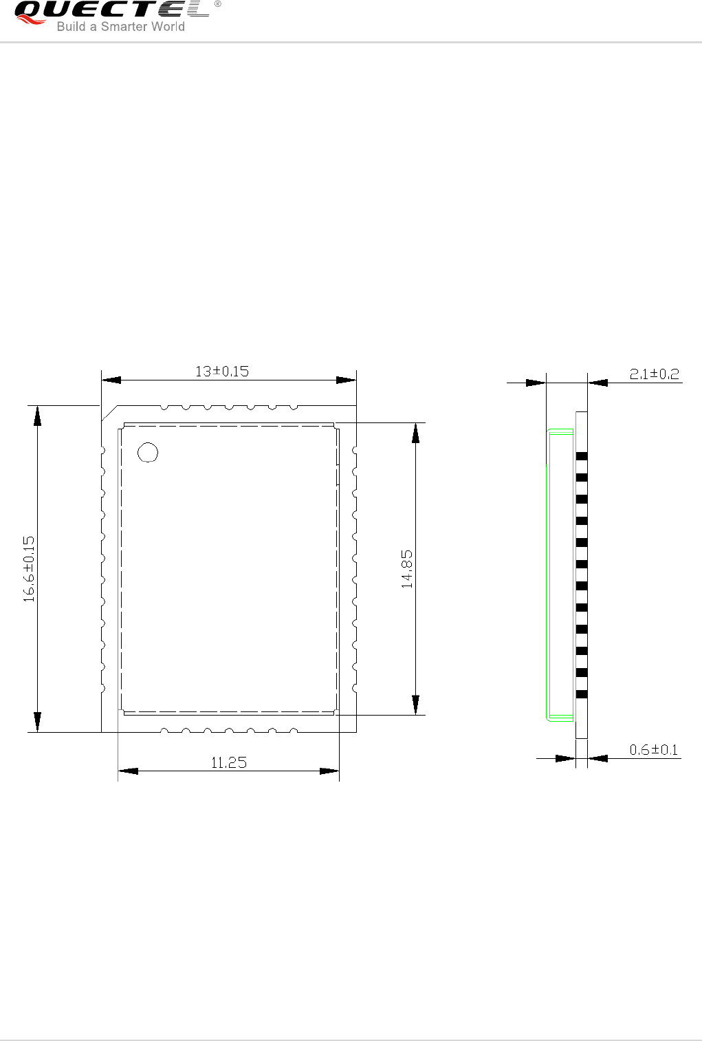
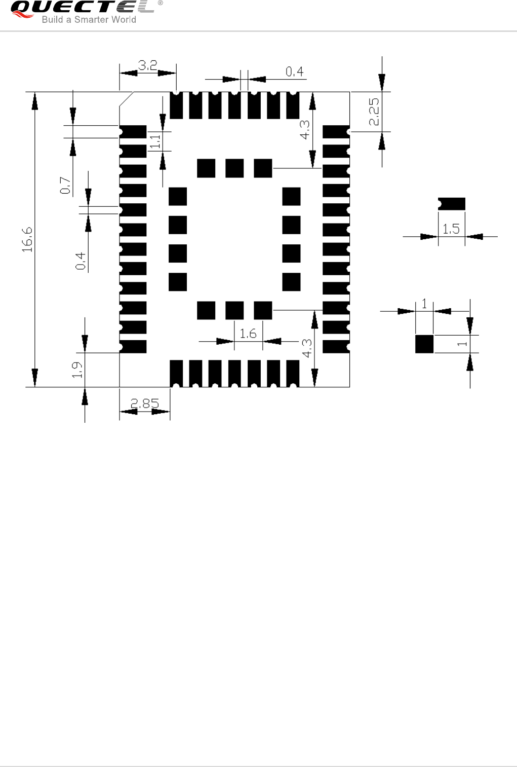
5 Mechanical Dimensions
This chapter describes the mechanical dimensions of FC20 series module.
5.1. Mechanical Dimensions of the Module
Figure 12: FC20 Top and Side Dimensions (Unit: mm)
FC20-N Series Hardware Design
FC20-N_Series_Hardware_Design Confidential / Released 36 /
47
Figure 13: FC20 Bottom Dimensions (Unit: mm)
FC20-N Series Hardware Design
FC20-N_Series_Hardware_Design Confidential / Released 37 /
47
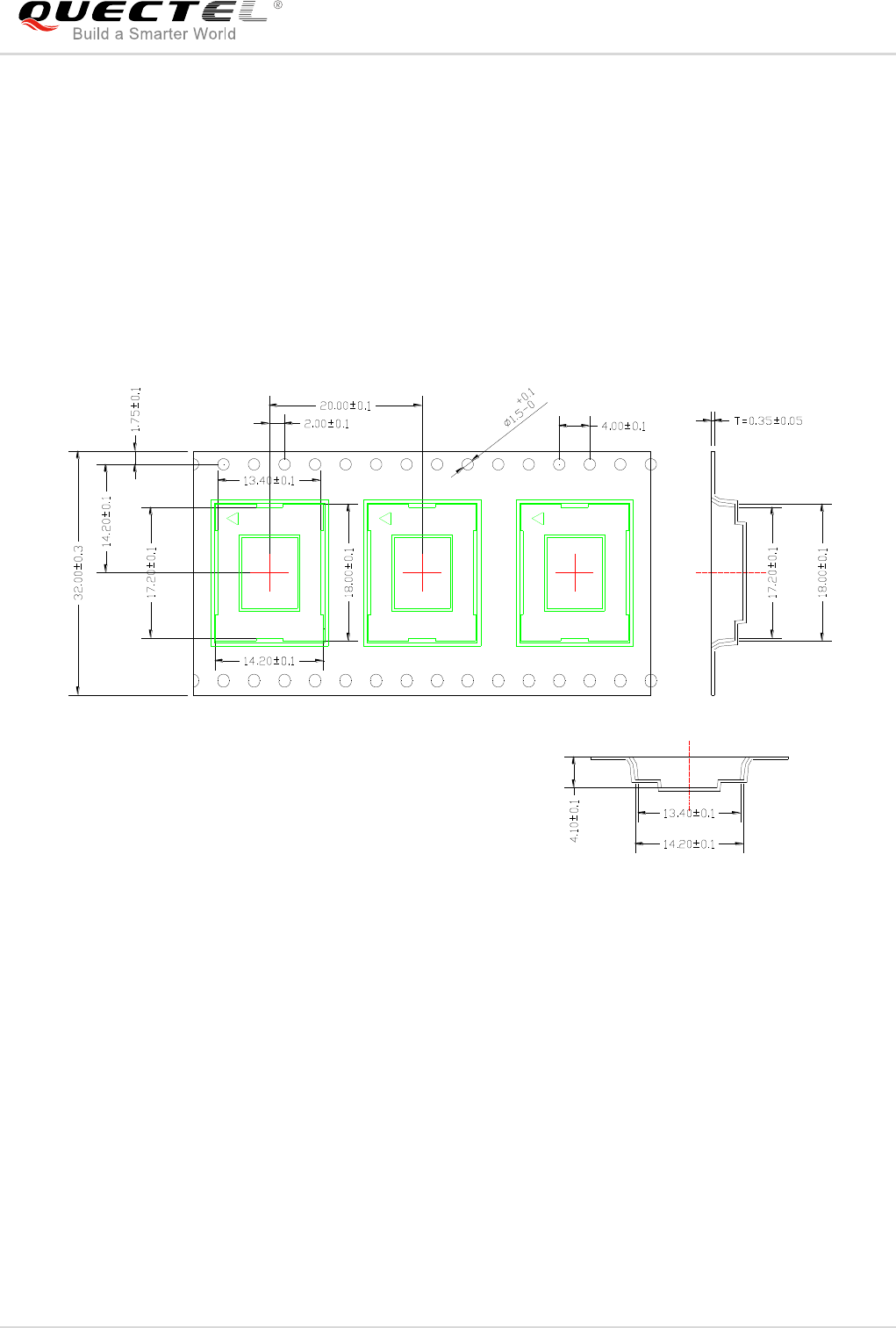
5.2. Recommended Footprint and Stencil
Figure 14: Recommended Footprint (Unit: mm)
FC20-N Series Hardware Design
FC20-N_Series_Hardware_Design Confidential / Released 38 /
47
The recommended stencil design for FC20 series is shown as below. To ensure the module soldering
quality, the thickness of stencil for the module is recommended to be 0.18mm.
Figure 15: Recommended Stencil (Unit: mm)
1. For easy maintenance of the module, please keep about 3mm between the module and other
components in host PCB.
2. Keep the RESERVED pins unconnected.
NOTES
FC20-N Series Hardware Design
FC20-N_Series_Hardware_Design Confidential / Released 39 /
47
5.3. Top and Bottom View of the Module
Figure 16: Top View of the Module
Figure 17: Bottom View of the Module
These are design effect drawings of FC20 series module. For more accurate pictures, please refer to the
module that you get from Quectel.
NOTE
FC20-N Series Hardware Design
FC20-N_Series_Hardware_Design Confidential / Released 40 /
47
6 Storage, Manufacturing and
Packaging
6.1. Storage
FC20 series module is stored in a vacuum-sealed bag. The storage restrictions are shown as below.
1. Shelf life in the vacuum-sealed bag: 12 months at <40ºC and <90% RH.
2. After the vacuum-sealed bag is opened, devices that need to be mounted directly must be:
Mounted within 72 hours at the factory environment of ≤30ºC and <60%RH.
Stored at <10% RH.
3. Devices require baking before mounting, if any circumstance below occurs.
When the ambient temperature is 23ºC±5ºC and the humidity indication card shows the humidity
is >10% before opening the vacuum-sealed bag.
Device mounting cannot be finished within 72 hours when the ambient temperature is <30ºC and the
humidity is <60%.
Stored at >10% RH.
4. If baking is required, devices should be baked for 48 hours at 125ºC±5ºC.
As the plastic package cannot be subjected to high temperature, it should be removed from devices
before high temperature (125ºC ) baking. If shorter baking time is desired, please refer to
IPC/JEDECJ-STD-033 for baking procedure.
NOTE
FC20-N Series Hardware Design
FC20-N_Series_Hardware_Design Confidential / Released 41 /
47
6.2. Soldering
Push the squeegee to apply the solder paste on the surface of stencil, thus making the paste fill the
stencil openings and then penetrate to the PCB. The force on the squeegee should be adjusted
properly so as to produce a clean stencil surface on a single pass. To ensure the module soldering
quality, the thickness of stencil for the module is recommended to be 0.18mm. For more details,
please refer to document [5].
It is suggested that the peak reflow temperature is from 235ºC to 245ºC (for SnAg3.0Cu0.5 alloy). The
absolute maximum reflow temperature is 260ºC. To avoid damage to the module caused by repeated
heating, it is suggested that the module should be mounted after reflow soldering for the other side of
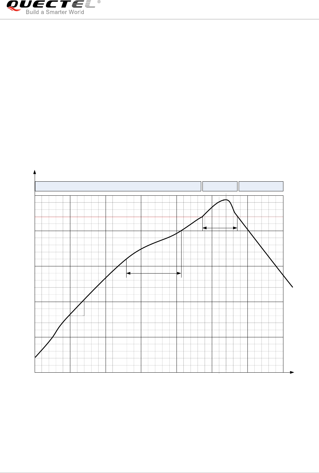
PCB has been completed. Recommended reflow soldering thermal profile is shown below:
Time (s)
50 100 150 200 250 300
50
100
150
200
250
160℃
200℃
217
0
70s~120s
40s~60s
Between 1~3℃/S
Preheat Heating Cooling
℃
s
Liquids
Temperature
Figure 18: Reflow Soldering Thermal Profile
FC20-N Series Hardware Design
FC20-N_Series_Hardware_Design Confidential / Released 42 /
47
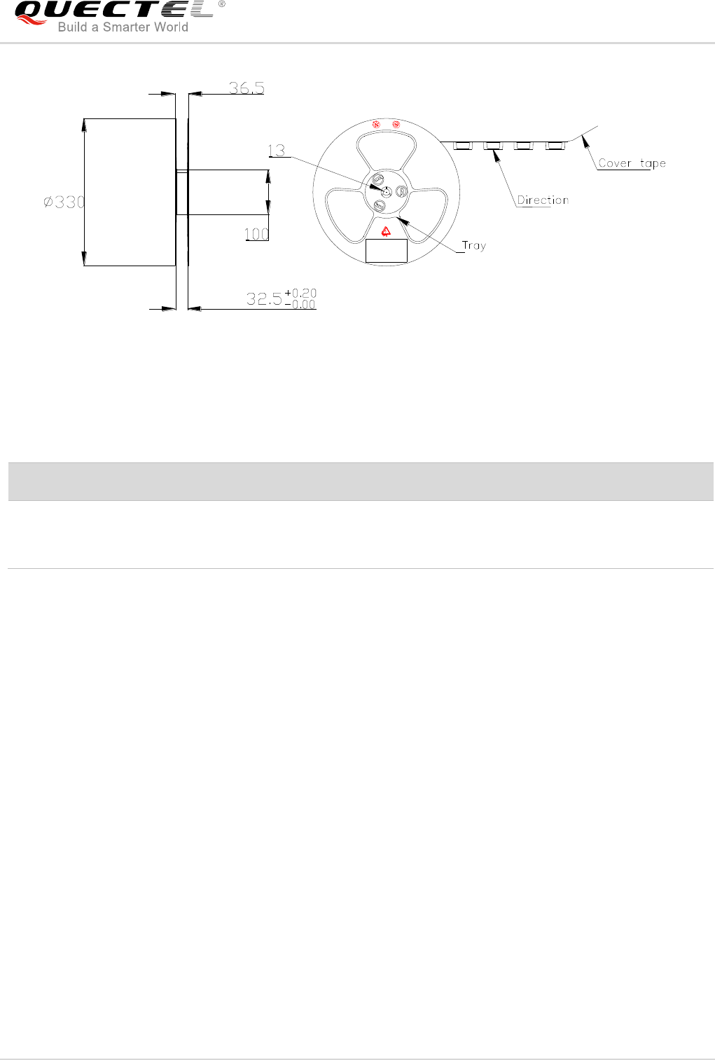
6.3. Packaging
FC20 module is packaged in a vacuum-sealed bag which is ESD protected. The bag should not be
opened until the devices are ready to be soldered onto the application.
6.3.1. Tape and Reel Packaging
FC20 is packaged in tape and reel carriers. The figures below show the packaging details.
Figure 19: Tape Dimensions (Unit: mm)
FC20-N Series Hardware Design
FC20-N_Series_Hardware_Design Confidential / Released 43 /
47
Figure 20: Reel Dimensions (Unit: mm)
Table 25: Reel Packaging
Model Name
MOQ for MP
Minimum Package: 250pcs
Minimum Package × 4=1000pcs
FC20-N
250pcs
Size: 370mm × 350mm × 56mm
N.W: 0.203kg
G.W: 0.945kg
Size: 380mm × 250mm × 365mm
N.W: 0.81kg
G.W: 4.33kg

FC20-N Series Hardware Design
FC20-N_Series_Hardware_Design Confidential / Released 44 /
47
7 Appendix A References
Table 26: Related Documents
SN
Document Name
Remark
[1]
Quectel_FC20_EVB_User_Guide
FC20 EVB user guide
[2]
Quectel_EC25_Reference_Design
EC25 reference design
[3]
Quectel_EC21_Reference_Design
EC21 reference design
[4]
Quectel_EC20_R2.0_Reference_Design
EC20 R2.0 reference design
[5]
Quectel_Module_Secondary_SMT_User_Guide
Module secondary SMT user guide
Table 27: Terms and Abbreviations
Abbreviation
Description
AP
Access Point
BPSK
Binary Phase Shift Keying
BT
Bluetooth
CCK
Complementary Code Keying
CTS
Clear To Send
ESD
Electrostatic Discharge
GND
Ground
HT
High Throughput
IEEE
Institute of Electrical and Electronics Engineers
IIL
Input Leakage Current
I/O
Input/Output

FC20-N Series Hardware Design
FC20-N_Series_Hardware_Design Confidential / Released 45 /
47
LTE
Long Term Evolution
Mbps
Million Bits Per Second
MCS
Modulation and Coding Scheme
MOQ
Minimum Order Quantity
MP
Manufacture Product
PCB
Printed Circuit Board
PCM
Pulse Code Modulation
QAM
Quadrature Amplitude Modulation
QPSK
Quadrature Phase Shift Keying
RF
Radio Frequency
RH
Relative Humidity
RoHS
Restriction of Hazardous Substances
RTS
Request To Send
RX
Receive Direction
SDIO
Secure Digital Input and Output Card
TBD
To Be Determined
TX
Transmitting Direction
UART
Universal Asynchronous Receiver Transmitter
USB
Universal Serial Bus
VDD
Voltage Power for Digital Device
VHT
Very High Throughput
VIHmax
Maximum Input High Level Voltage Value
VIHmin
Minimum Input High Level Voltage Value
VILmax
Maximum Input Low Level Voltage Value
VILmin
Minimum Input Low Level Voltage Value

FC20-N Series Hardware Design
FC20-N_Series_Hardware_Design Confidential / Released 46 /
47
VIO
Voltage for Input/Output Port
VOLmax
Maximum Output Low Level Voltage Value
VOHmin
Minimum Output High Level Voltage Value
VSWR
Voltage Standing Wave Ratio
Wi-Fi
Wireless-Fidelity
WLAN
Wireless Local Area Networks