Quectel Wireless Solutions 201708EC21E LTE Module User Manual XMR201708EC21E Rev1
Quectel Wireless Solutions Company Limited LTE Module XMR201708EC21E Rev1
UserManual.wiki
>
Quectel Wireless Solutions
>
201708EC21E User Manual
User Manual
Navigation menu
Upload a User Manual
Namespaces
Wiki Guide
HTML
PDF
Info
Views
User Manual
Discussion / Help
Navigation

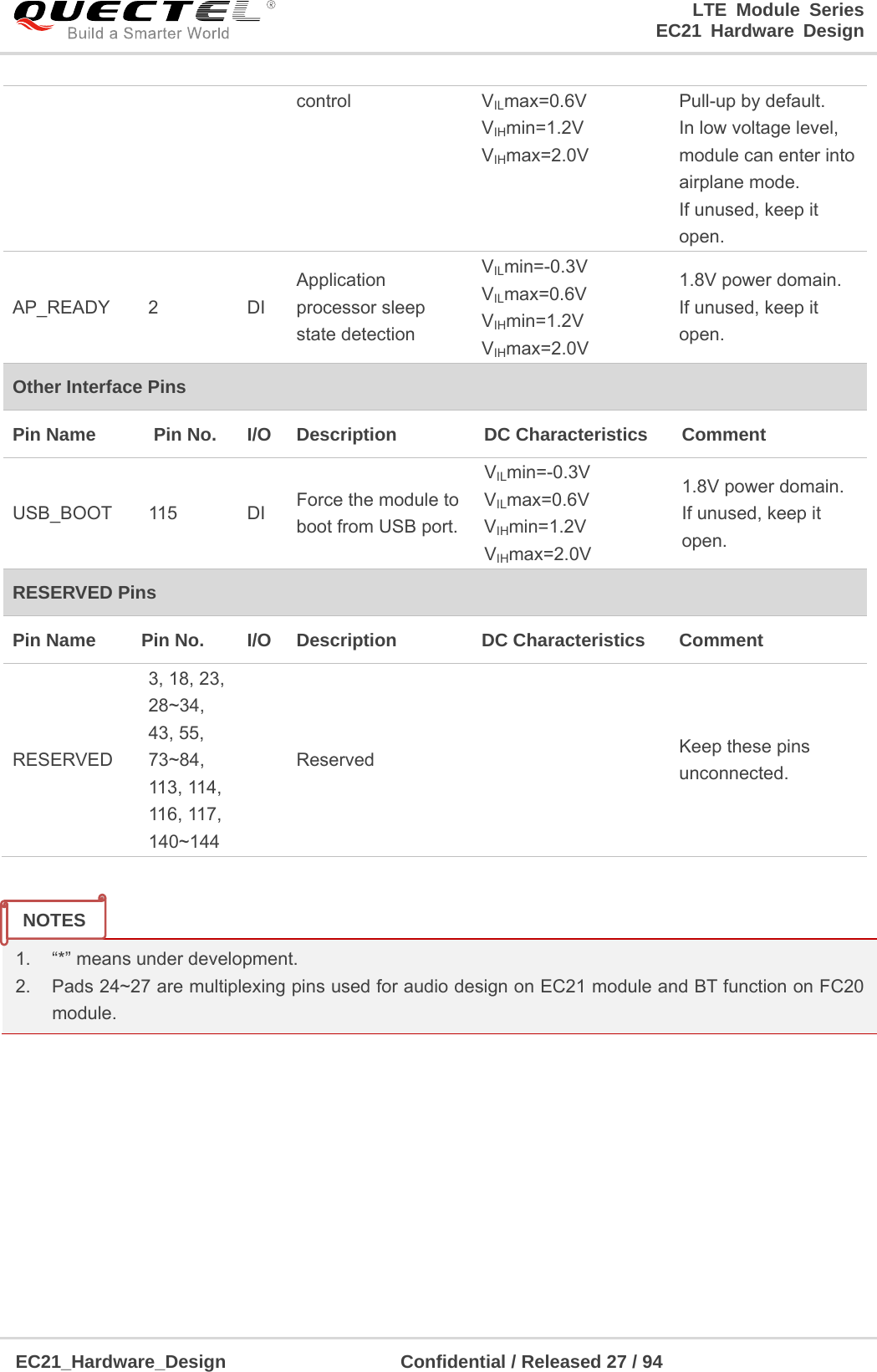
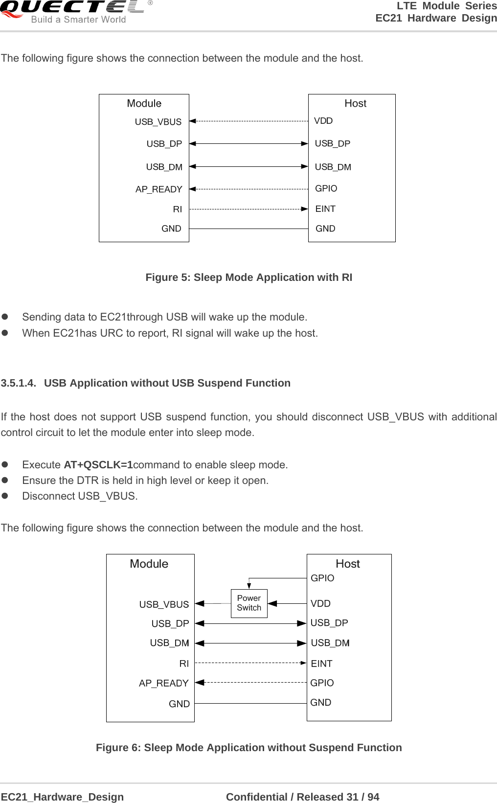
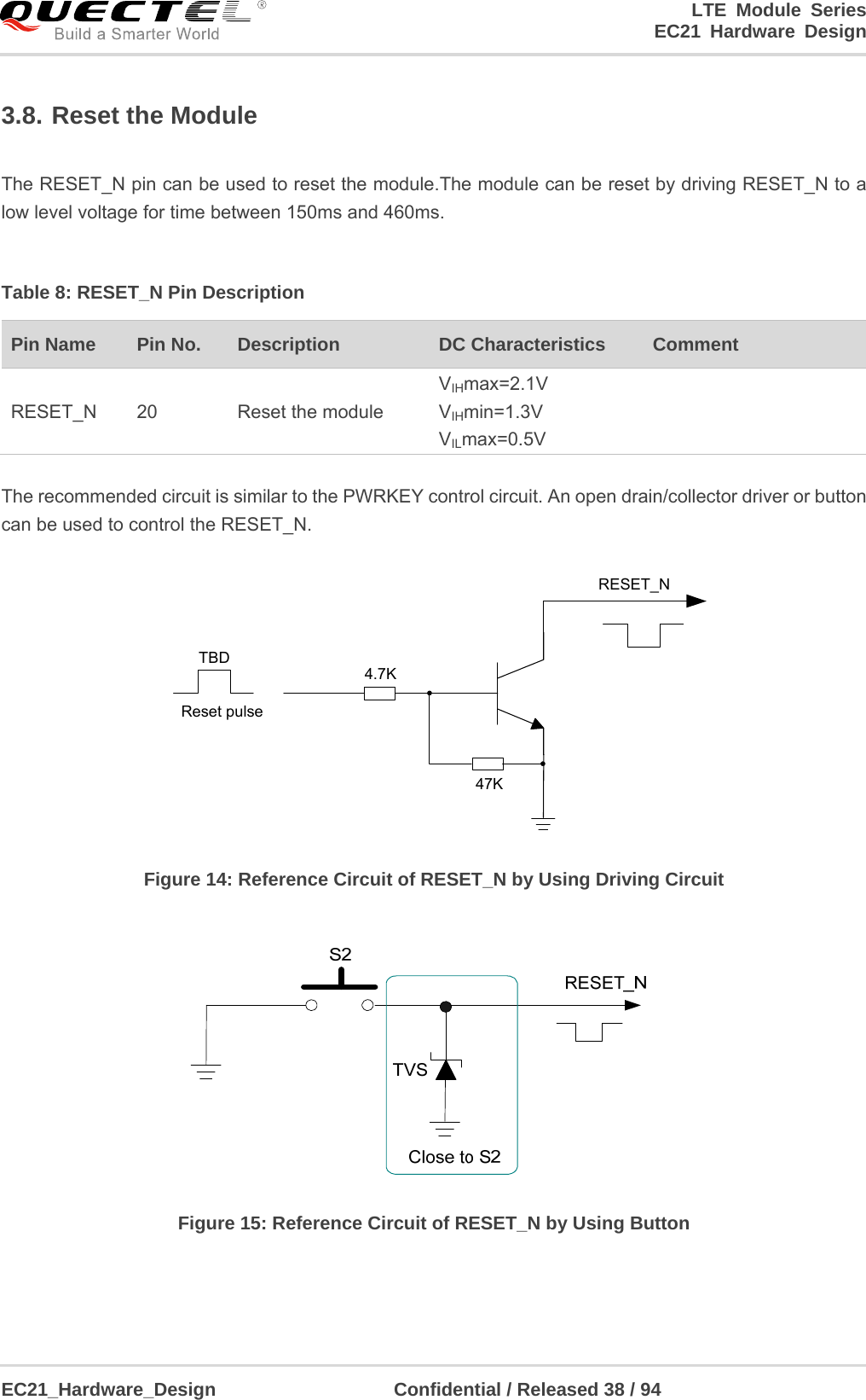
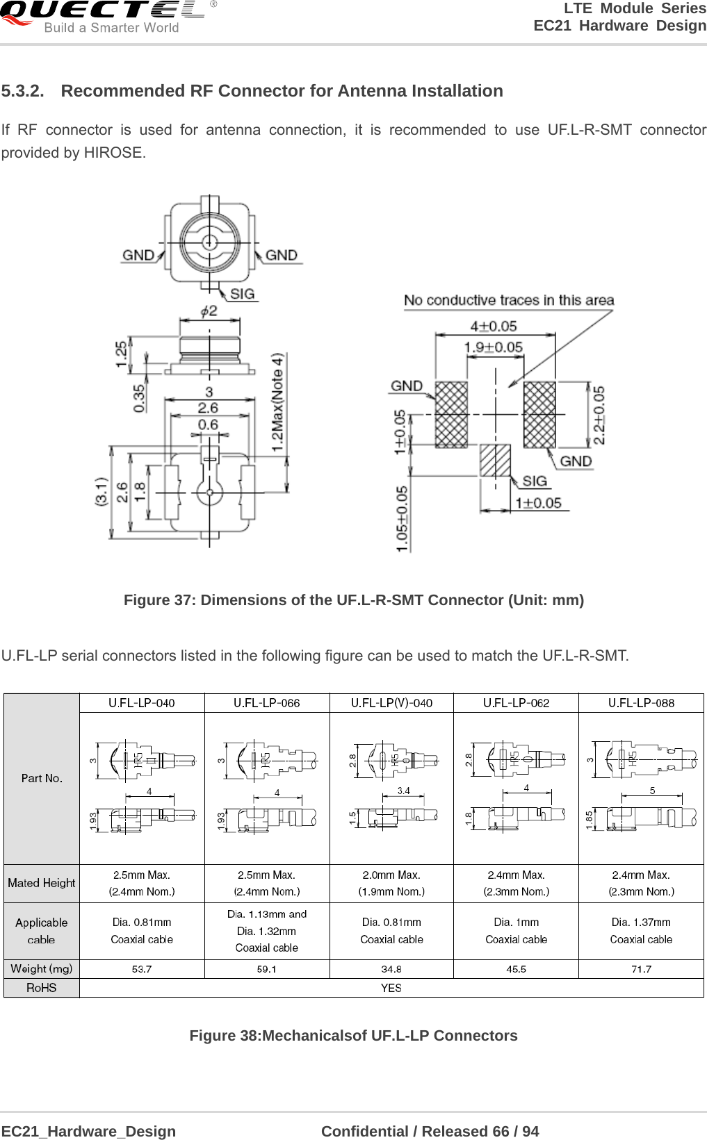
![LTE Module Series EC21 Hardware Design EC21_Hardware_Design Confidential / Released 32 / 94 Switching on the power switch to supply power to USB_VBUS will wake up the module. Please pay attention to the level match shown in dotted line between the module and thehost.Refer to document [1] for more details about EC21 power management application. 3.5.2. Airplane Mode When the module enters into airplane mode, the RF function does not work, and all AT commands correlative with RF function will be inaccessible. This mode can be set via the following ways. Hardware: The W_DISABLE# pin is pulled up by default;driving it to low level will let the module enter into airplane mode. Software: AT+CFUNcommand provides the choice of the functionality level. AT+CFUN=0: Minimum functionality mode;both USIM and RF functions are disabled. AT+CFUN=1: Full functionality mode (by default). AT+CFUN=4: Airplane mode. RF function is disabled. 1. The W_DISABLE# control function is disabled in firmware by default. It can be enabled by AT+QCFG=“airplanecontrol” command. This commandis under development. 2. The execution of AT+CFUN command will not affect GNSS function. 3.6. Power Supply 3.6.1. Power Supply Pins EC21 provides four VBAT pins for connection with the external power supply. There are two separate voltage domains for VBAT. Two VBAT_RF pins for module RF part. Two VBAT_BB pins for module baseband part. The following table shows the details of VBAT pins and ground pins. NOTES NOTE](https://usermanual.wiki/Quectel-Wireless-Solutions/201708EC21E/User-Guide-3519741-Page-33.png)
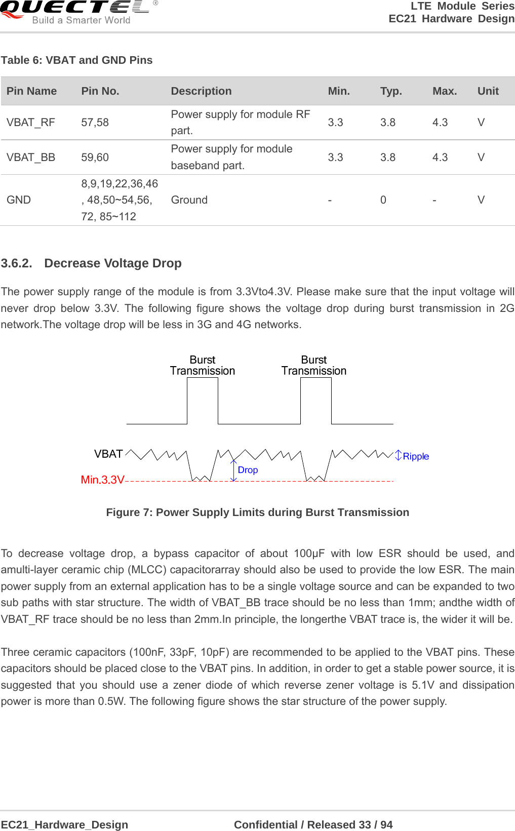
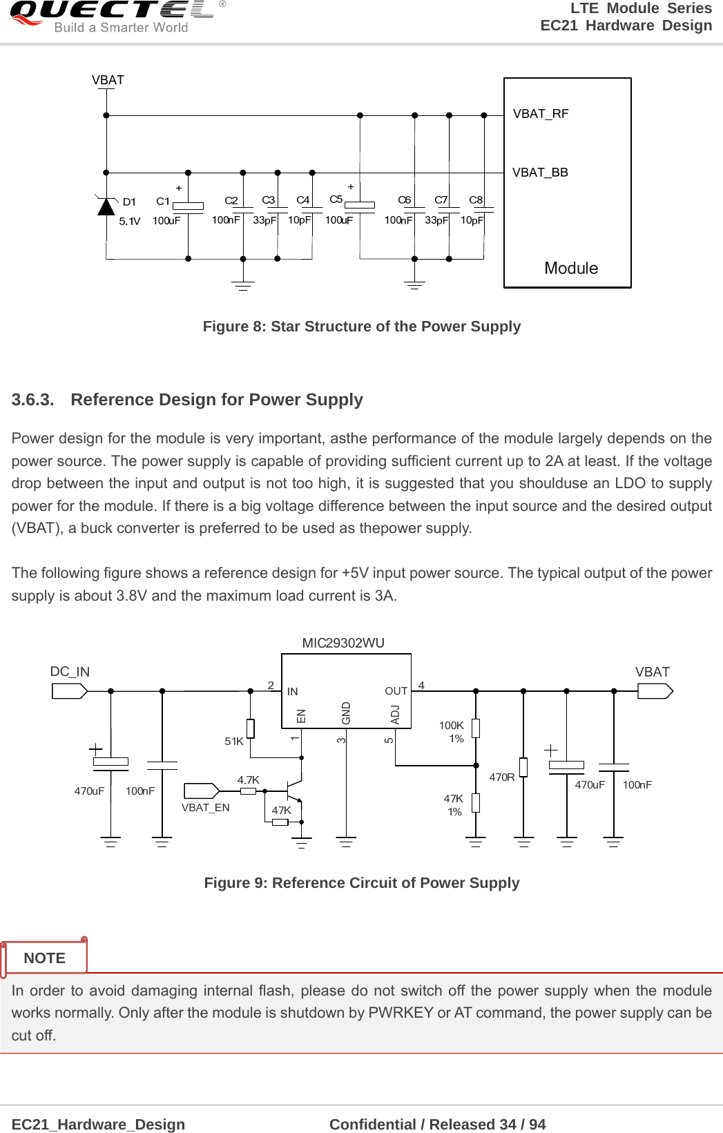
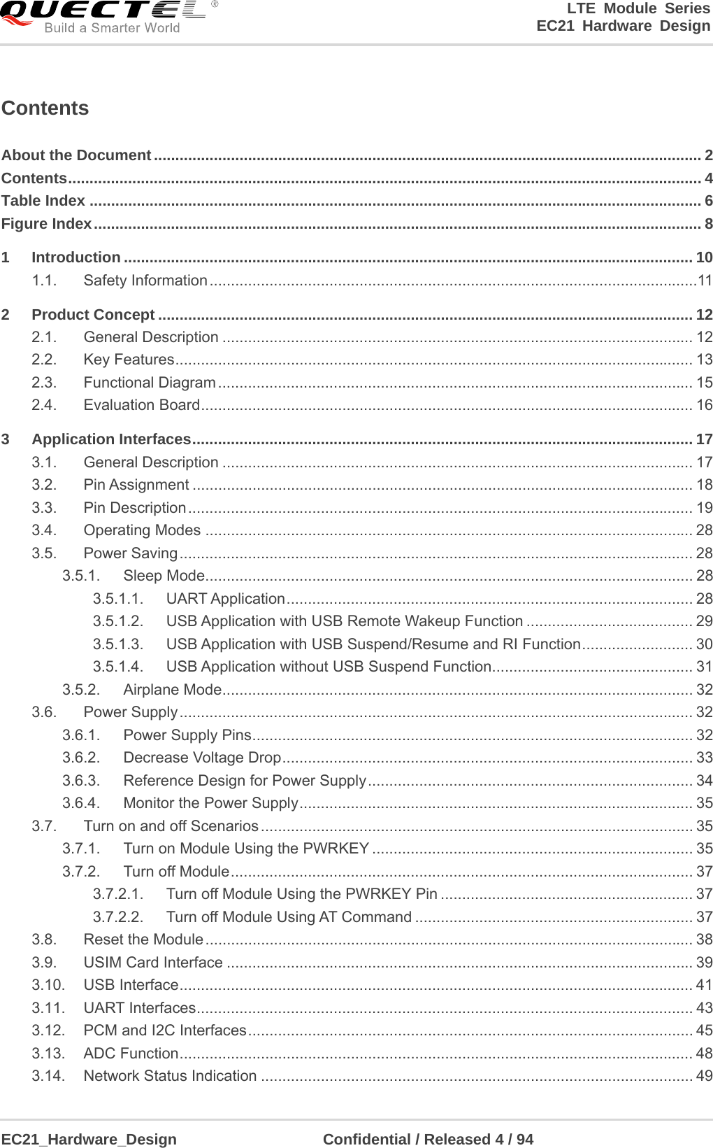
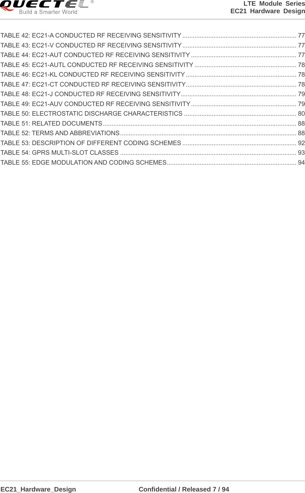
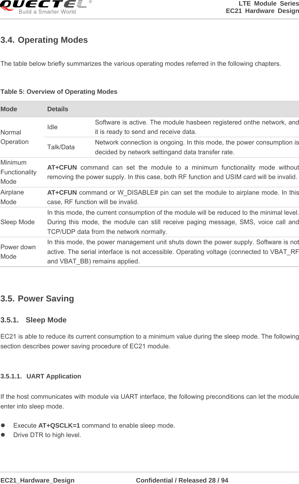
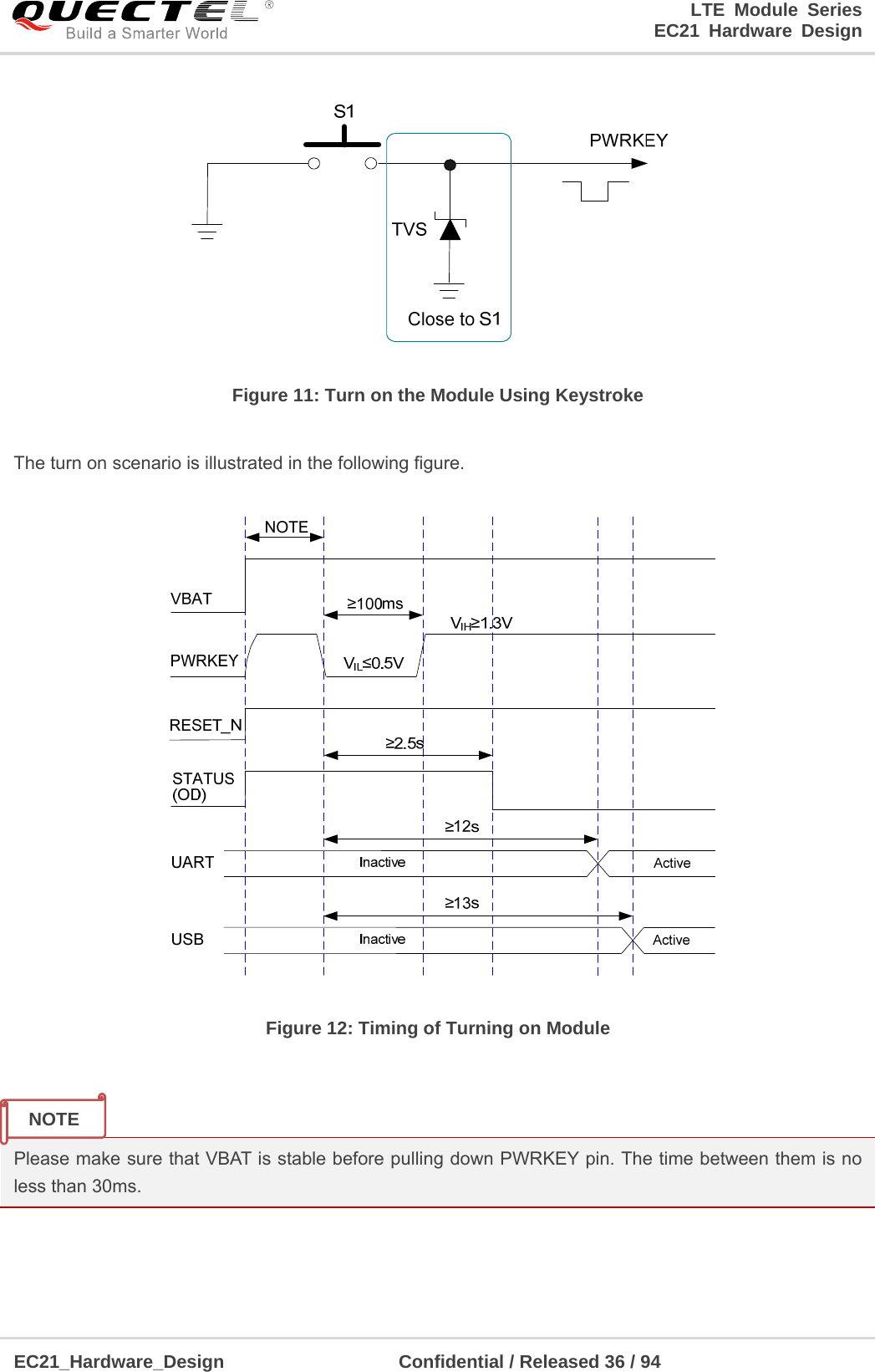
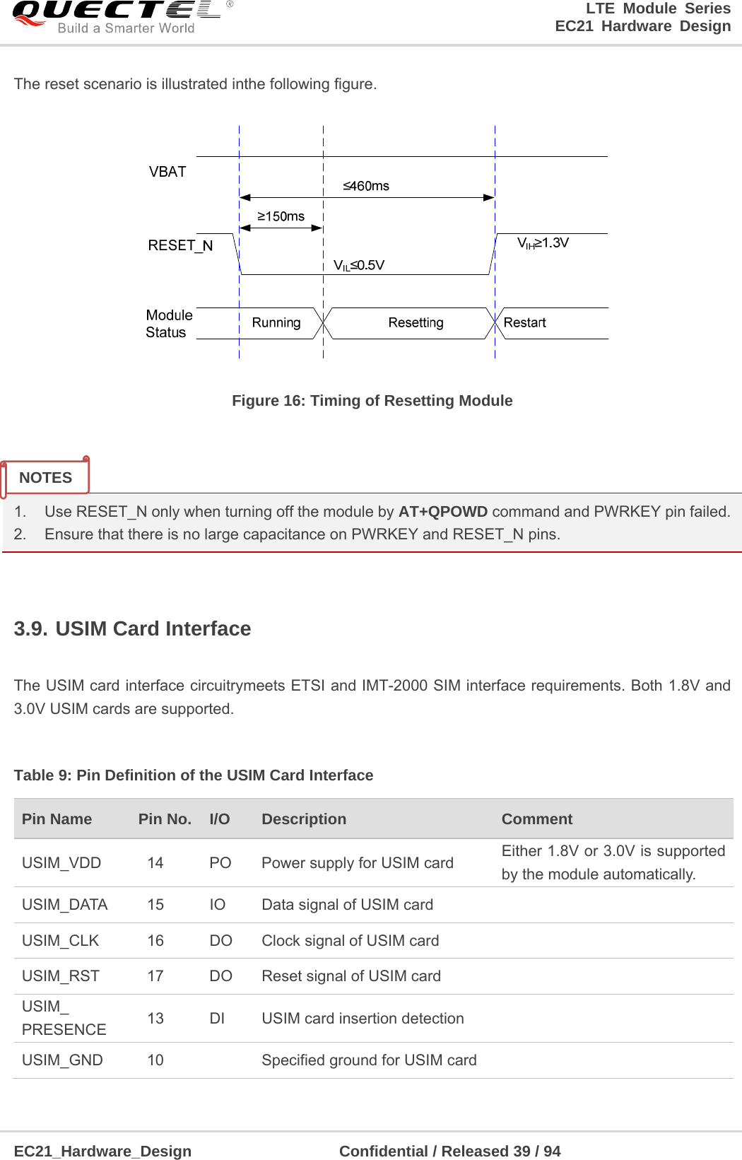
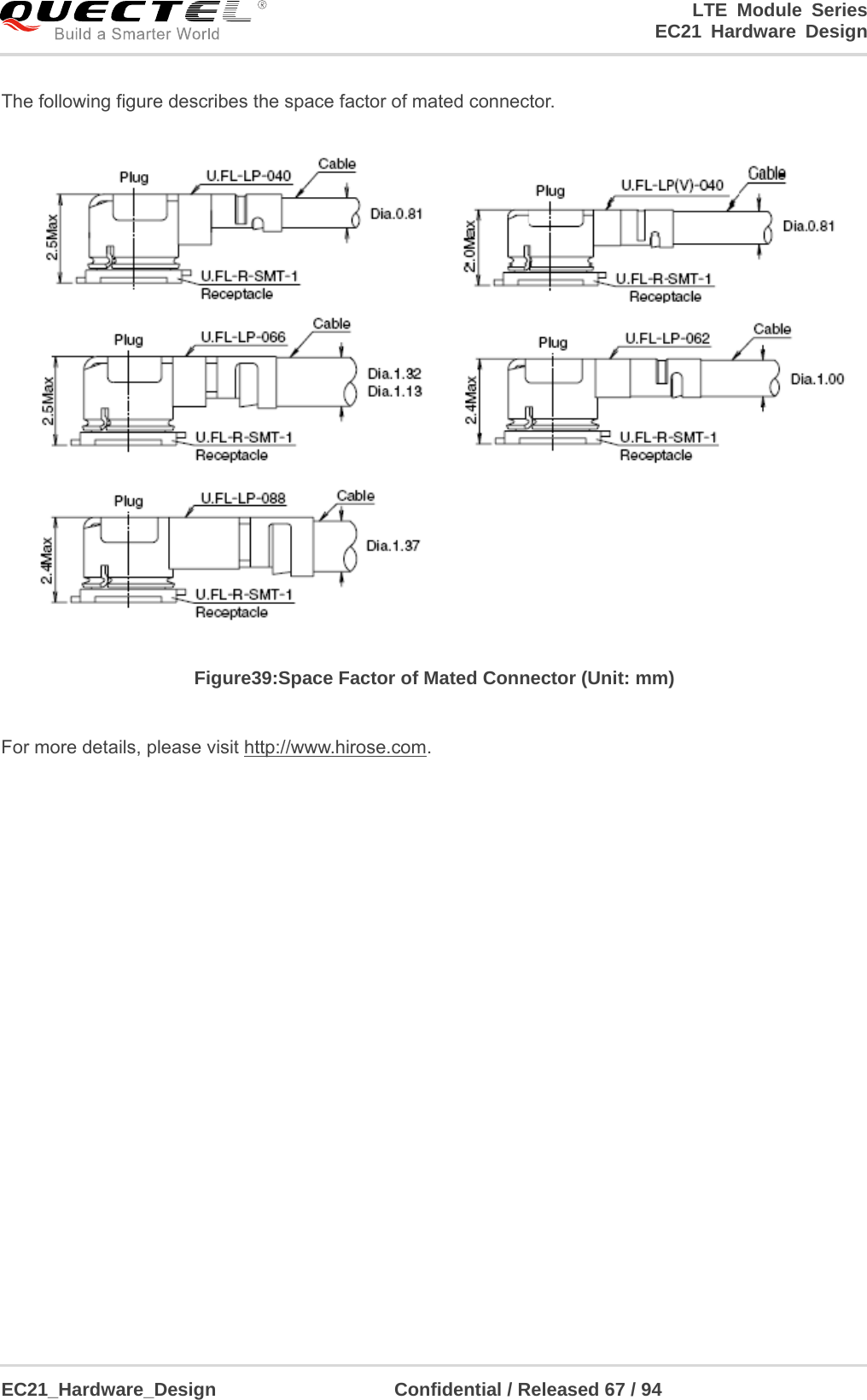
![LTE Module Series EC21 Hardware Design EC21_Hardware_Design Confidential / Released 35 / 94 3.6.4. Monitor the Power Supply AT+CBC command can be used to monitor the VBAT_BB voltage value. For more details, please refer to document [2]. 3.7. Turn on and off Scenarios 3.7.1. Turn on Module Using the PWRKEY The following table shows the pin definition of PWRKEY. Table 7: PWRKEY Pin Description Pin Name Pin No. Description DC Characteristics Comment PWRKEY 21 Turn on/off the module VIHmax=2.1V VIHmin=1.3V VILmax=0.5V The output voltage is 0.8V because of the diode drop in the Qualcomm chipset. When EC21 is in power down mode, it can be turned on to normal mode by driving the PWRKEY pin to a low level for at least 100ms. It is recommended to use an open drain/collector driver to control the PWRKEY.After STATUS pin (require external pull-up) outputting a low level, PWRKEY pin can be released. A simple reference circuit is illustrated in the following figure. Figure 10: Turn on the Module Using Driving Circuit The other way to control the PWRKEY is using a button directly. When pressing the key, electrostatic strike may generate from finger. Therefore, a TVS component is indispensable to be placed nearby the button for ESD protection. A reference circuit is shownin the following figure.](https://usermanual.wiki/Quectel-Wireless-Solutions/201708EC21E/User-Guide-3519741-Page-36.png)
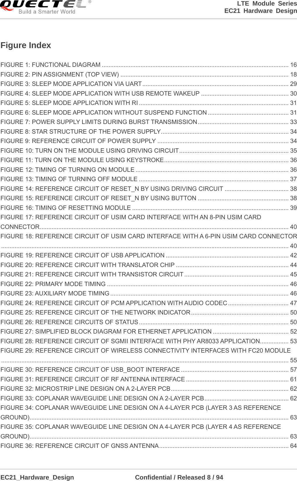
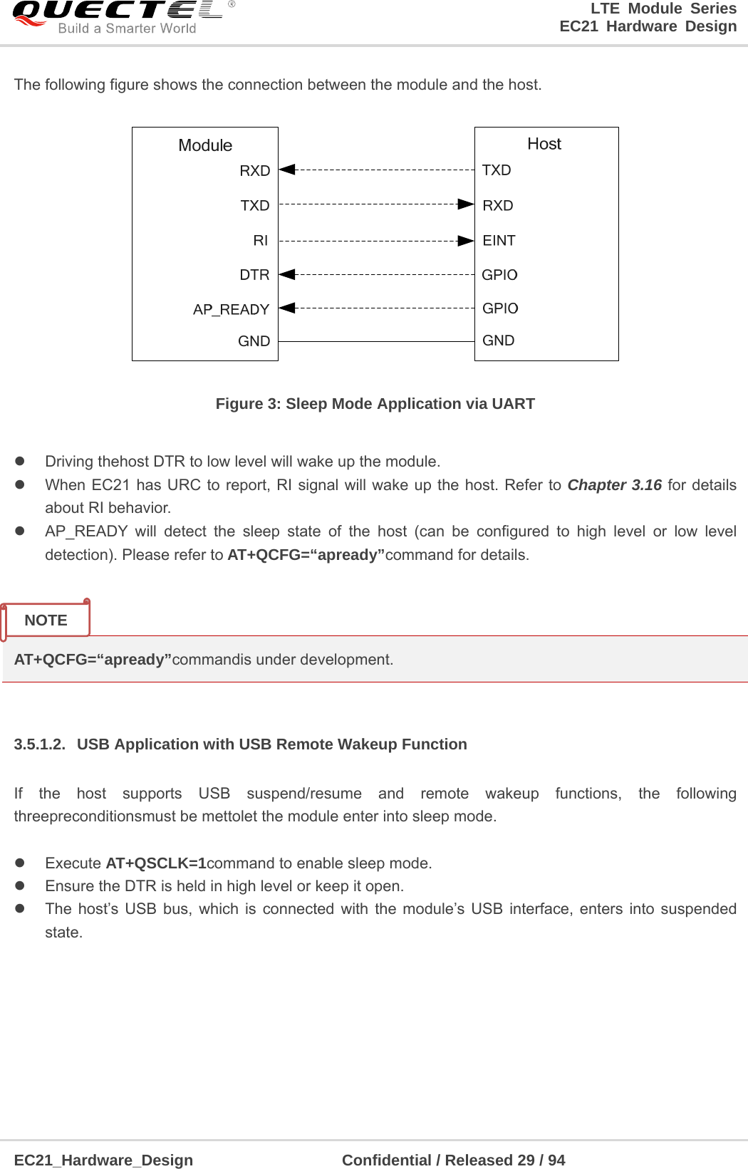
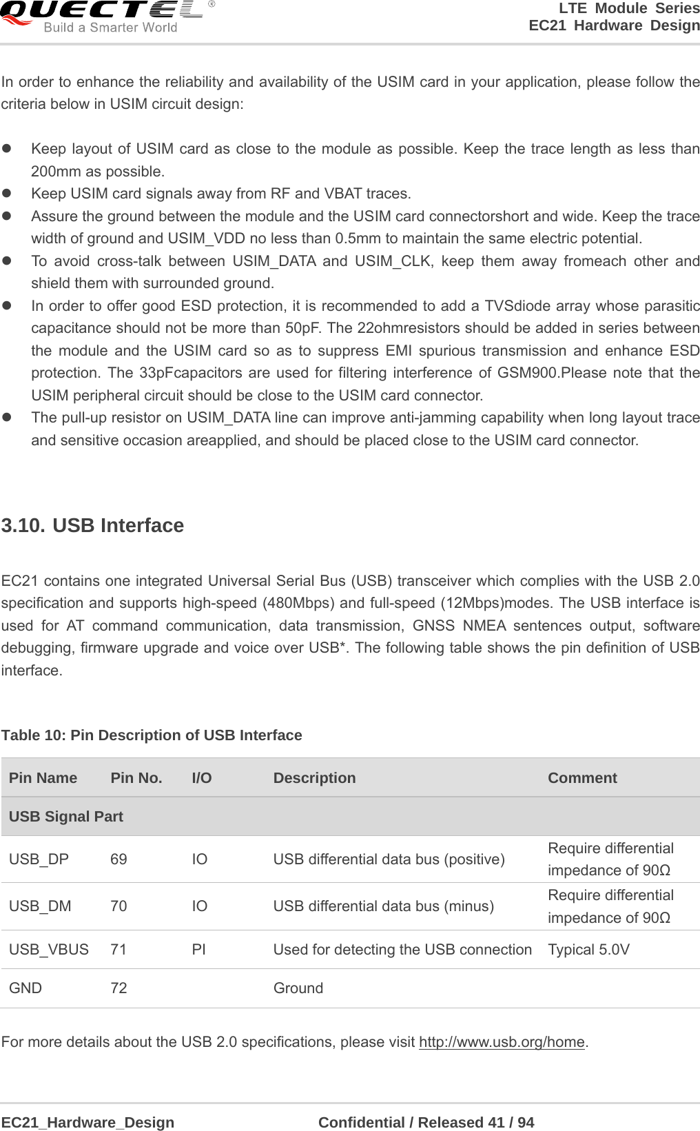
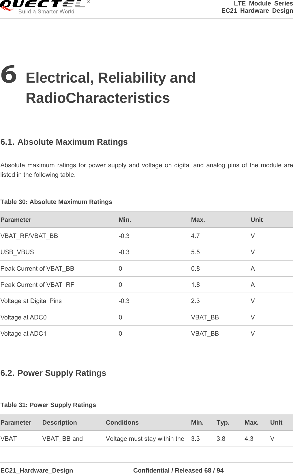
![LTE Module Series EC21 Hardware Design EC21_Hardware_Design Confidential / Released 37 / 94 3.7.2. Turn off Module The following procedures can be used to turn off the module: Normal power down procedure: Turn off the module using the PWRKEY pin. Normal power down procedure: Turn off the module using AT+QPOWD command. 3.7.2.1. Turn off Module Using the PWRKEY Pin Driving the PWRKEY pin to a low level voltagefor at least 650ms, the module will execute power-down procedure after the PWRKEY is released. The power-down scenario is illustrated inthe following figure. Figure 13: Timing of Turning off Module 3.7.2.2. Turn off Module Using AT Command It is also a safe way to use AT+QPOWDcommandto turn off the module, which is similar to turning off the module via PWRKEY pin. Please refer todocument [2] for details about AT+QPOWD command. In order to avoid damaging internal flash, please do not switch off the power supply when the module works normally. Only after the module is shutdown by PWRKEY or AT command, the power supply can be cut off. NOTE](https://usermanual.wiki/Quectel-Wireless-Solutions/201708EC21E/User-Guide-3519741-Page-38.png)
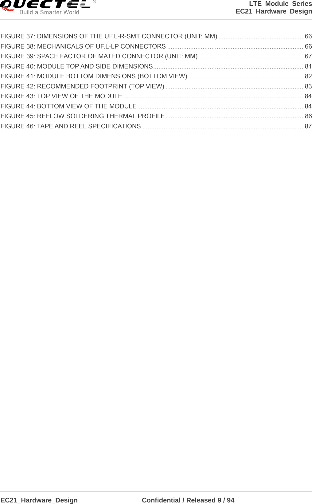
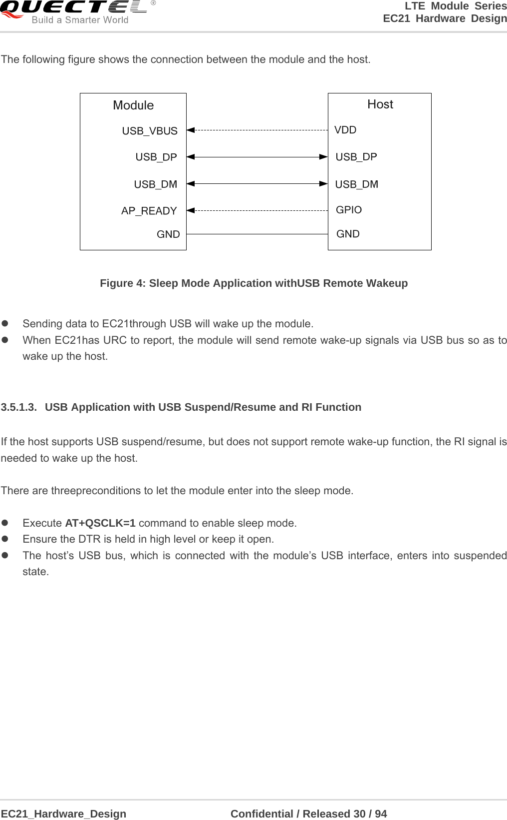
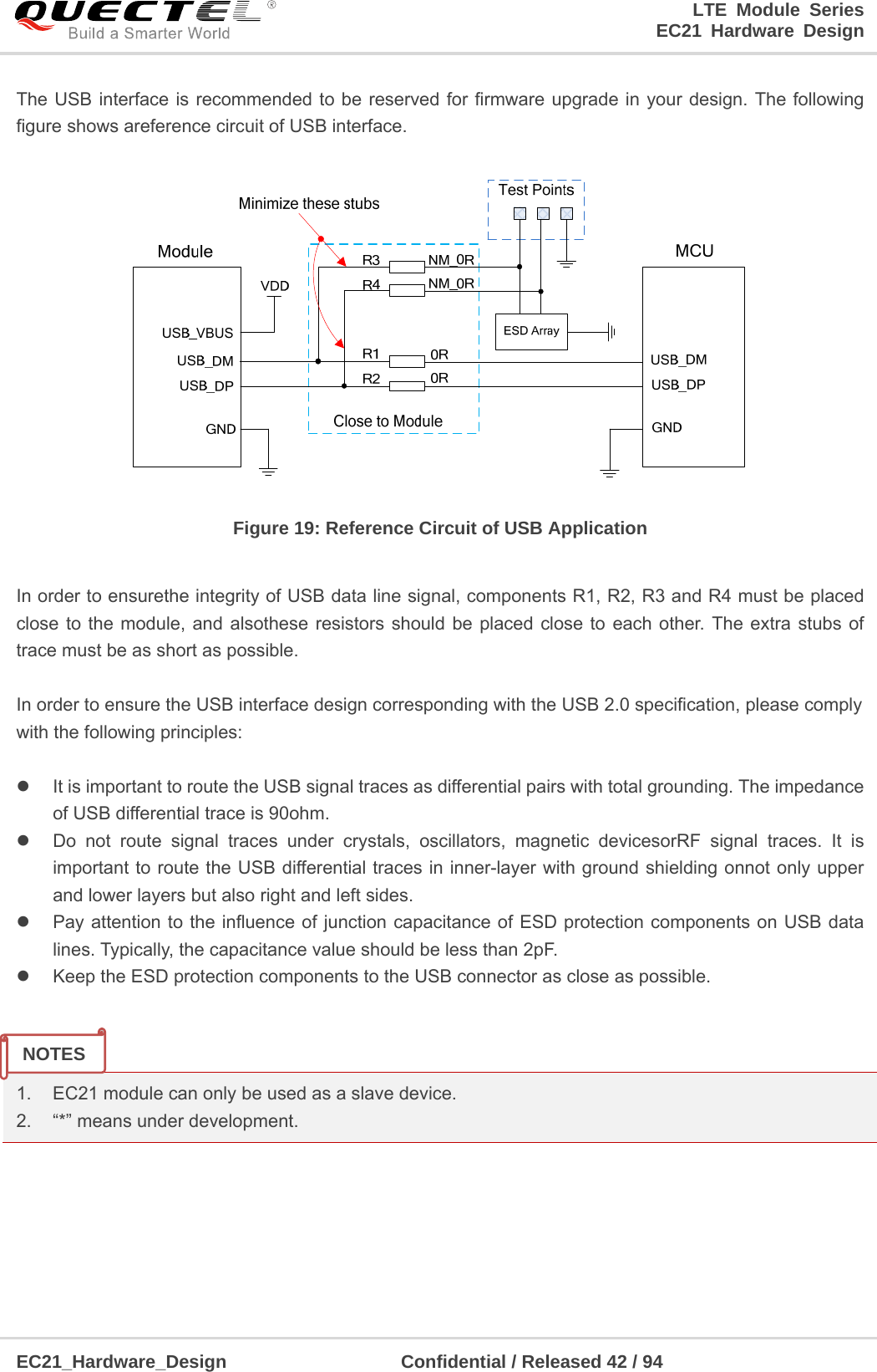
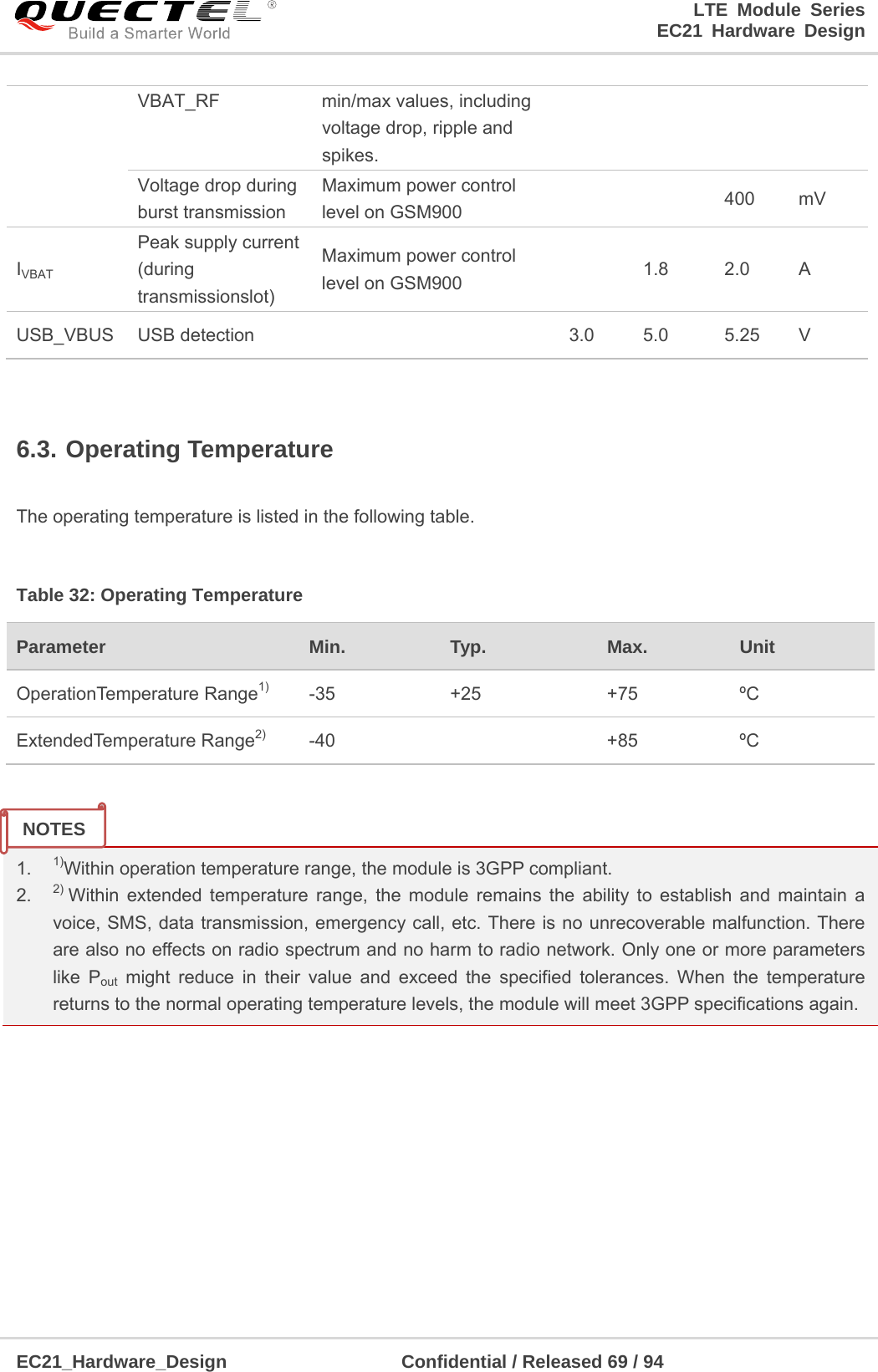
![LTE Module Series EC21 Hardware Design EC21_Hardware_Design Confidential / Released 40 / 94 EC21 supports USIM card hot-plug via the USIM_PRESENCE pin. The function supports low level and high level detections, and is disabled by default. Please refer to document [2] about AT+QSIMDET command for details. The following figure shows a reference design for USIM card interface with an 8-pin USIM card connector. Figure 17: Reference Circuit of USIM Card Interface with an 8-Pin USIM Card Connector If USIM card detection function is not needed, please keep USIM_PRESENCE unconnected. Areference circuit for USIM card interface with a 6-pin USIM card connector is illustrated inthe following figure. Figure 18: Reference Circuit of USIM Card Interface with a6-Pin USIM Card Connector](https://usermanual.wiki/Quectel-Wireless-Solutions/201708EC21E/User-Guide-3519741-Page-41.png)
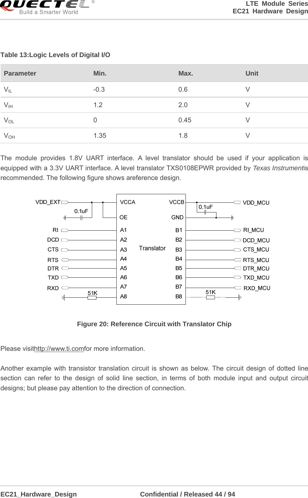
![LTE Module Series EC21 Hardware Design EC21_Hardware_Design Confidential / Released 47 / 94 PCM_CLK 27 IO PCM data bit clock 1.8V power domain I2C_SCL 41 OD I2C serial clock Require external pull-up to 1.8V I2C_SDA 42 OD I2C serial data Require external pull-up to 1.8V Clock and mode can be configured by AT command, and the default configuration is master mode using short frame synchronization format with 2048kHzPCM_CLK and 8kHz PCM_SYNC.Please refer to document [2] about AT+QDAIcommand for details. The following figure shows areference design of PCM interface with external codec IC. Figure 24: Reference Circuit of PCM Application with Audio Codec 1. “*” means under development. 2. It is recommended to reserve RC (R=22ohm, C=22pF) circuit on the PCM lines, especially for PCM_CLK. 3. EC21 works as a master device pertaining to I2C interface. NOTES](https://usermanual.wiki/Quectel-Wireless-Solutions/201708EC21E/User-Guide-3519741-Page-48.png)
![LTE Module Series EC21 Hardware Design EC21_Hardware_Design Confidential / Released 48 / 94 3.13. ADC Function The module provides two analog-to-digital converters (ADC).AT+QADC=0 command can be used to read the voltage value on ADC0 pin. AT+QADC=1command can be used to read the voltage value on ADC1 pin. For more details about these AT commands, please refer todocument [2]. In order to improve the accuracy of ADC, the trace of ADC should be surrounded by ground. Table 15: Pin Definition of the ADC Pin Name Pin No. Description ADC0 45 General purpose analog to digital converter ADC1 44 General purpose analog to digital converter The following table describes the characteristic of the ADC function. Table 16: Characteristic of the ADC Parameter Min. Typ. Max. Unit ADC0 Voltage Range 0.3 VBAT_BB V ADC1 Voltage Range 0.3 VBAT_BB V ADC Resolution 15 bits 1. ADC input voltage must not exceed VBAT_BB. 2. It is prohibited to supply any voltage to ADC pins when VBAT is removed. 3. It is recommended to use resistor divider circuit for ADC application. NOTES](https://usermanual.wiki/Quectel-Wireless-Solutions/201708EC21E/User-Guide-3519741-Page-49.png)
![LTE Module Series EC21 Hardware Design EC21_Hardware_Design Confidential / Released 51 / 94 3.16. Behavior of the RI AT+QCFG=“risignaltype”,“physical” command can be usedto configure RI behavior. No matter on which port URC is presented, URC will trigger the behavior of RI pin. URC can be output from UART port, USB AT port and USB modem port by AT+QURCCFG command. The default port is USB AT port. In addition, RI behavior can be configured flexibly. The default behavior of the RI is shown as below. Table 20: Behavior of the RI State Response Idle RI keeps in high level URC RI outputs 120ms low pulse when new URC returns The RI behavior can be changed by AT+QCFG=“urc/ri/ring”command.Please refer to document [2] for details. 3.17. SGMII Interface EC21 includes an integrated Ethernet MAC with an SGMII interface and two management interfaces, key features of the SGMII interface are shown below: IEEE802.3 compliance Full duplex at 1000Mbps Half/full duplex for 10/100Mbps Support VLAN tagging Support IEEE1588 and Precision Time Protocol (PTP) Can be used to connect to external Ethernet PHY like AR8033, or to an external switch Management interfaces support dual voltage 1.8V/2.85V The following table shows the pin definition of SGMII interface. NOTE](https://usermanual.wiki/Quectel-Wireless-Solutions/201708EC21E/User-Guide-3519741-Page-52.png)
![LTE Module Series EC21 Hardware Design EC21_Hardware_Design Confidential / Released 53 / 94 Figure 28: Reference Circuit of SGMII Interface with PHY AR8033 Application In order to enhance the reliability and availability in your application, please follow the criteria below in the Ethernet PHY circuit design: Keep SGMII data and control signals away from RF and VBAT trace. Keep the maximum trace length less than 10inch and keep skew on the differential pairs less than 20mil. The differential impedance of SGMII data trace is 100ohm±10%. To minimize crosstalk, the distance between separate adjacent pairs that are on the same layer must be equal to or larger than 40mil. For more information about SGMII application, please refer to document [5]and document[7]. NOTE](https://usermanual.wiki/Quectel-Wireless-Solutions/201708EC21E/User-Guide-3519741-Page-54.png)
![LTE Module Series EC21 Hardware Design EC21_Hardware_Design Confidential / Released 56 / 94 1. FC20 module can only be used as a slave device, 2. When BT function is enabled on EC21 module, PCM_SYNC and PCM_CLK pins are only used to output signals. 3. For more information about wireless connectivity interfaces, please refer to document [5]. 3.18.1. WLAN Interface EC21 provides a low power SDIO 3.0 interface and control interface for WLAN design. SDIO interface supports the following modes: Single data rate (SDR) mode (up to 200MHz) Double data rate (DDR) mode (up to 52MHz) As SDIO signals are very high-speed, in order to ensure the SDIO interface design corresponds with the SDIO 3.0 specification, please comply with the following principles: It is important to route the SDIO signal traces with total grounding. The impedance of SDIOsignal trace is 50ohm (±10%). Protect other sensitive signals/circuits (RF, analog signals, etc.) from SDIO corruption and protect SDIO signals from noisy signals (clocks, DCDCs, etc.). It is recommended to keep matching lengthbetween CLK and DATA/CMD less than 1mm and total routing length less than 50mm. Keep termination resistors within 15~24ohm on clock lines near the module and keep the route distance from the module clock pins to termination resistors less than 5mm. Make sure the adjacent trace spacing is 2x line width and bus capacitance is less than 15pF. 3.18.2. BT Interface* EC21 supports a dedicated UART interface and a PCM interface for BTfunction application. Further information about BT interface will be added in future version of this document. “*” means under development. NOTES NOTE](https://usermanual.wiki/Quectel-Wireless-Solutions/201708EC21E/User-Guide-3519741-Page-57.png)
![LTE Module Series EC21 Hardware Design EC21_Hardware_Design Confidential / Released 58 / 94 4 GNSS Receiver 4.1. General Description EC21 includes a fully integrated global navigation satellite system solution that supports Gen8C-Liteof Qualcomm (GPS, GLONASS, BeiDou, Galileo and QZSS). EC21 supports standard NMEA-0183 protocol, and outputs NMEA sentences at 1Hz data update ratevia USB interface by default. By default, EC21 GNSS engine is switched off. It has to be switched on via AT command. For more details about GNSS engine technology and configurations, please refer to document [3]. 4.2. GNSS Performance The following table shows the GNSS performance of EC21. Table 24: GNSS Performance Parameter Description Conditions Typ. Unit Sensitivity (GNSS) Cold start Autonomous -146 dBm Reacquisition Autonomous -157 dBm Tracking Autonomous -157 dBm TTFF (GNSS) Cold start @open sky Autonomous 35 s XTRA enabled 18 s Warm start @open sky Autonomous 26 s XTRA enabled 2.2 s](https://usermanual.wiki/Quectel-Wireless-Solutions/201708EC21E/User-Guide-3519741-Page-59.png)
![LTE Module Series EC21 Hardware Design EC21_Hardware_Design Confidential / Released 63 / 94 Figure 34: Coplanar Waveguide Line Design on a 4-layer PCB (Layer 3 as Reference Ground) Figure 35: Coplanar Waveguide Line Design on a 4-layer PCB (Layer 4 as Reference Ground) In order to ensure RF performance and reliability, the following principles should be complied with in RF layout design: Use impedance simulation tool to control the characteristic impedanceof RF tracesas 50ohm. The GND pins adjacent to RF pins should not be hot welded, and should be fully connected to ground. The distance between the RF pinsand the RFconnector should be as short as possible, and all the right angle traces should be changed to curved ones. There should be clearance area under the signal pin of the antenna connector or solder joint. The reference ground of RF traces should be complete. Meanwhile, adding some ground viasaround RF traces and the reference ground could help to improve RF performance. The distance between the ground vias and RF traces should be no less than two times the width of RF signal traces (2*W). For more details about RF layout, please refer to document [6].](https://usermanual.wiki/Quectel-Wireless-Solutions/201708EC21E/User-Guide-3519741-Page-64.png)
![LTE Module Series EC21 Hardware Design EC21_Hardware_Design Confidential / Released 86 / 94 8.2. Manufacturing and Soldering Push the squeegee to apply the solder paste on the surface of stencil, thus making the paste fill the stencil openings and then penetrate to the PCB. The force on the squeegee should be adjusted properlyso as to produce a clean stencil surface on a single pass. To ensure the module soldering quality, thethickness of stencil for the module is recommended to be 0.18mm. For more details, please refer todocument [4]. It is suggested that the peak reflow temperature is from 235 to 245ºC (for SnAg3.0Cu0.5 alloy). The absolute maximum reflow temperature is 260ºC. To avoid damage to the module caused by repeated heating, it is suggested that the module should be mounted after reflow soldering for the other side of PCB has been completed. Recommended reflow soldering thermal profile is shown below: Figure 45: Reflow Soldering Thermal Profile During manufacturing and soldering, or any other processes that may contact the module directly, NEVER wipe the module label with organic solvents, such as acetone, ethyl alcohol, isopropyl alcohol, trichloroethylene, etc. NOTE](https://usermanual.wiki/Quectel-Wireless-Solutions/201708EC21E/User-Guide-3519741-Page-87.png)
![LTE Module Series EC21 Hardware Design EC21_Hardware_Design Confidential / Released 88 / 94 9 Appendix A References Table 51: Related Documents SN Document Name Remark [1] Quectel_EC21_Power_Management_Application_Note EC21 Power Management Application Note [2] Quectel_EC25&EC21_AT_Commands_Manual EC25 and EC21 AT Commands Manual[3] Quectel_EC25&EC21_GNSS_AT_Commands_Manual EC25 and EC21GNSS AT Commands Manual [4] Quectel_Module_Secondary_SMT_User_Guide Module Secondary SMT User Guide [5] Quectel_EC21_Reference_Design EC21 Reference Design [6] Quectel_RF_Layout_Application_Note RF Layout Application Note [7] Quectel_SGMII_Design_Application_Note SGMII Design Application Note Table 52: Terms and Abbreviations Abbreviation Description AMR Adaptive Multi-rate bps Bits Per Second CHAP Challenge Handshake Authentication Protocol CS Coding Scheme CSD Circuit Switched Data CTS Clear To Send DC-HSPA+ Dual-carrier High Speed Packet Access DFOTA Delta Firmware Upgrade Over The Air](https://usermanual.wiki/Quectel-Wireless-Solutions/201708EC21E/User-Guide-3519741-Page-89.png)