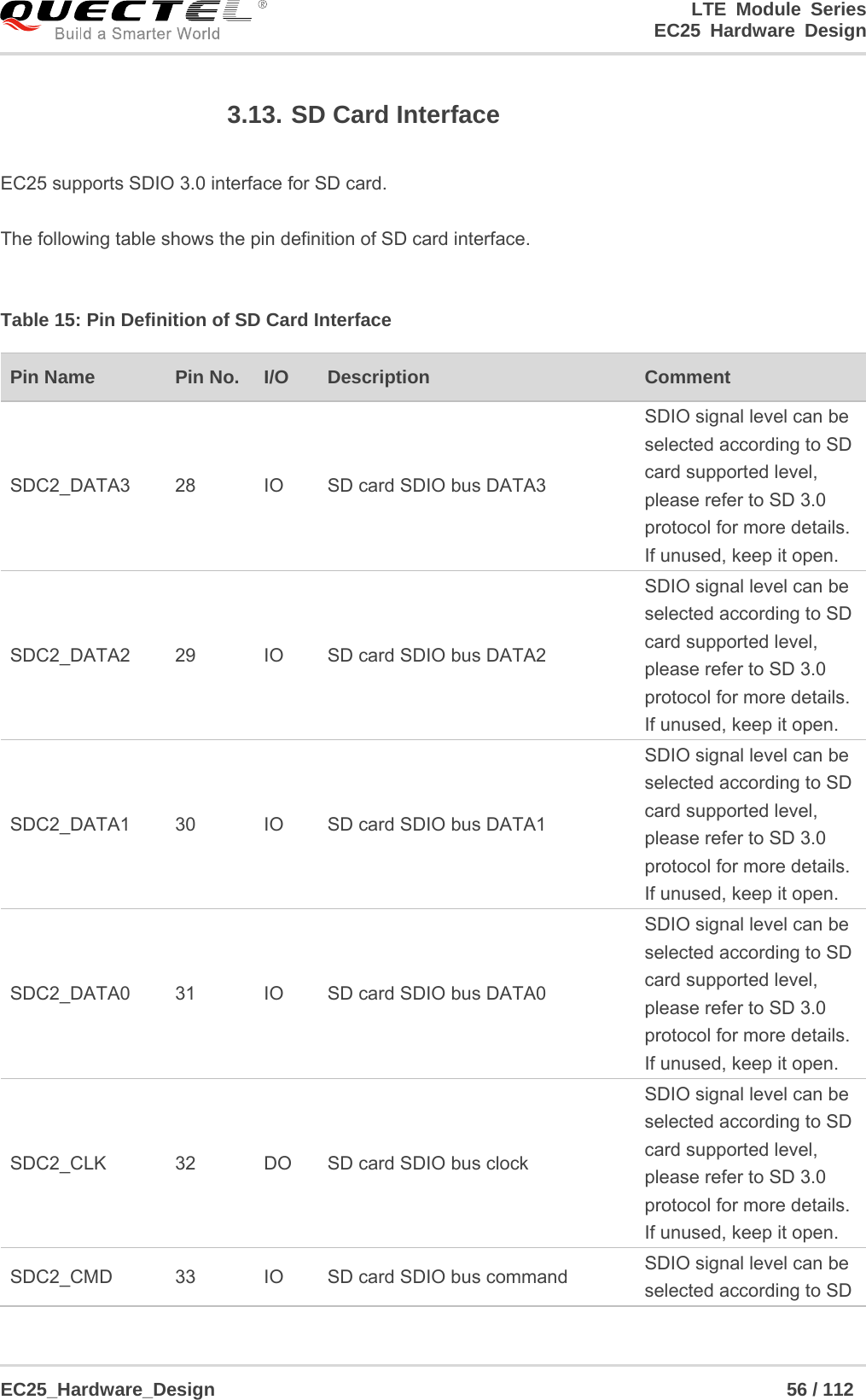
Quectel Wireless Solutions 201805EC25AU LTE Module User Manual
Quectel Wireless Solutions Company Limited LTE Module Users Manual
UserManual.wiki
>
Quectel Wireless Solutions
>
201805EC25AU User Manual
>
Users Manual
Contents
1.
Users Manual
2.
User Manual
Users Manual
Navigation menu
Upload a User Manual
Namespaces
Wiki Guide
HTML
PDF
Info
Views
User Manual
Discussion / Help
Navigation
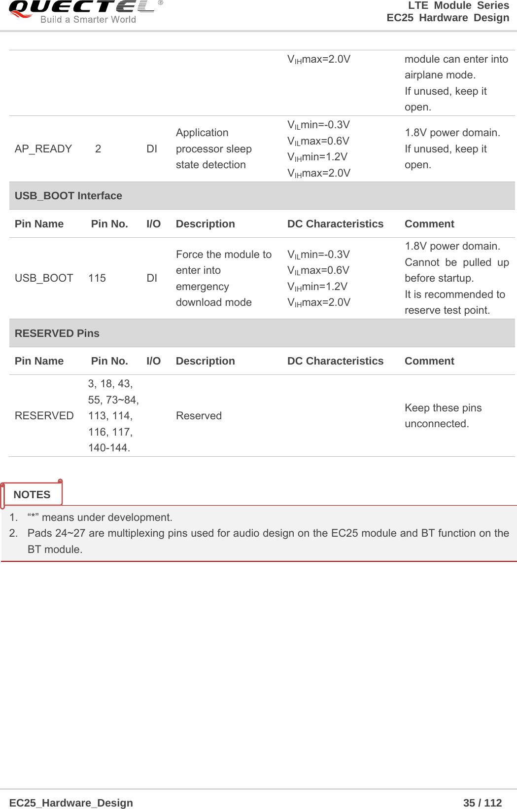
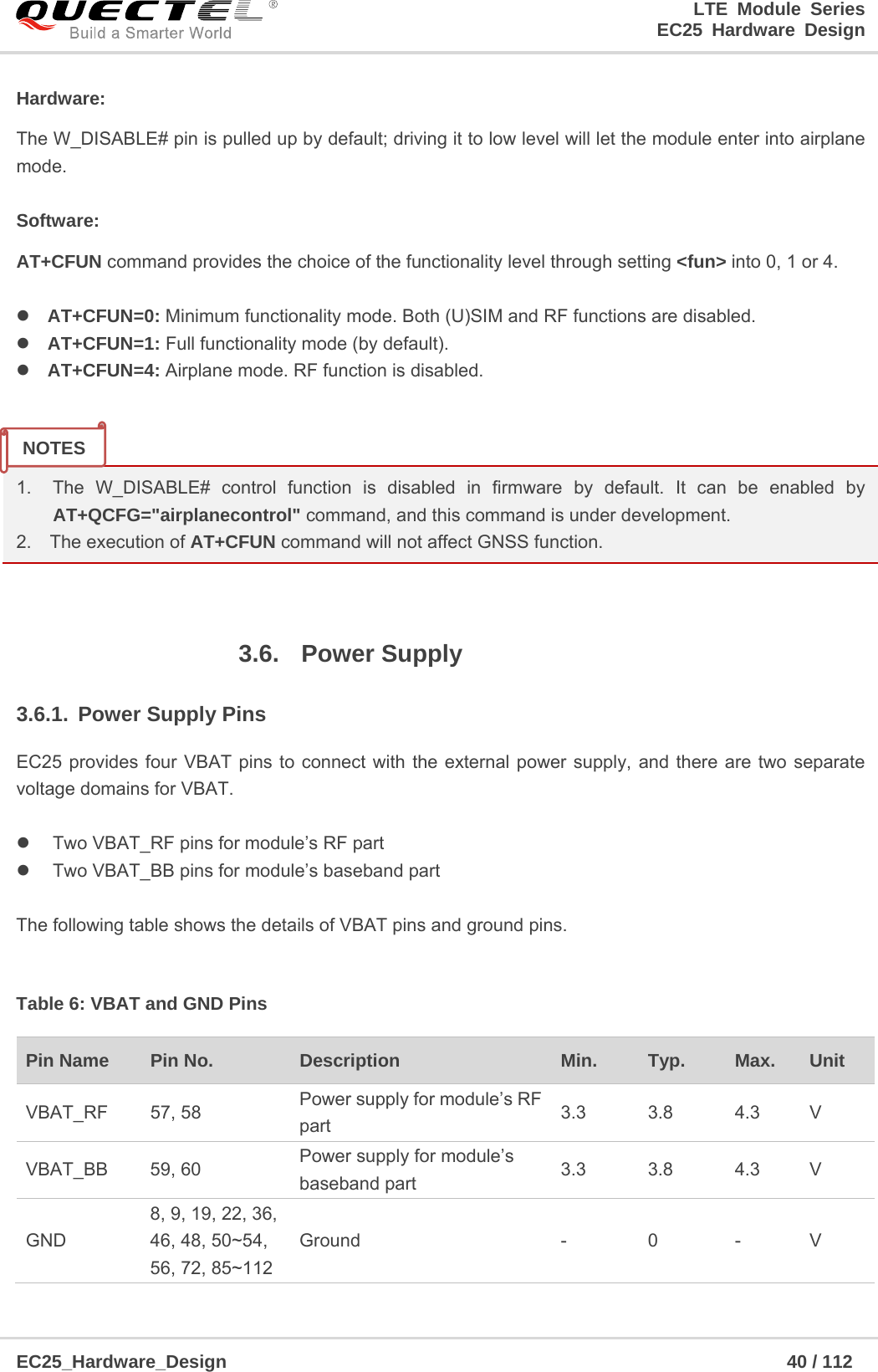
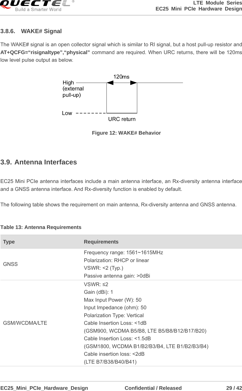
![LTE Module Series EC25 Hardware Design EC25_Hardware_Design 39 / 112 Sending data to EC25 through USB will wake up the module. When EC25 has a URC to report, RI signal will wake up the host. 3.5.1.4. USB Application without USB Suspend Function If the host does not support USB suspend function, USB_VBUS should be disconnected via an additional control circuit to let the module enter into sleep mode. Execute AT+QSCLK=1 command to enable sleep mode. Ensure the DTR is held at high level or keep it open. Disconnect USB_VBUS. The following figure shows the connection between the module and the host. Figure 6: Sleep Mode Application without Suspend Function Switching on the power switch to supply power to USB_VBUS will wake up the module. Please pay attention to the level match shown in dotted line between the module and the host. For more details about EC25 power management application, please refer to document [1]. 3.5.2. Airplane Mode When the module enters into airplane mode, the RF function does not work, and all AT commands correlative with RF function will be inaccessible. This mode can be set via the following ways. NOTE](https://usermanual.wiki/Quectel-Wireless-Solutions/201805EC25AU.Users-Manual/User-Guide-3839081-Page-40.png)
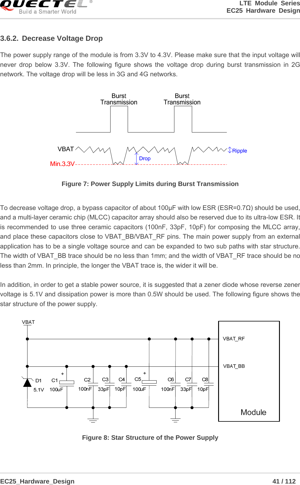
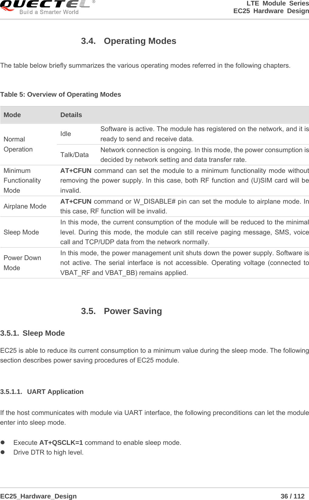
![LTE Module Series EC25 Hardware Design EC25_Hardware_Design 42 / 112 3.6.3. Reference Design for Power Supply Power design for the module is very important, as the performance of the module largely depends on the power source. The power supply should be able to provide sufficient current up to 2A at least. If the voltage drop between the input and output is not too high, it is suggested that an LDO should be used to supply power for the module. If there is a big voltage difference between the input source and the desired output (VBAT), a buck converter is preferred to be used as the power supply. The following figure shows a reference design for +5V input power source. The typical output of the power supplyis about 3.8V and the maximum load current is 3A. Figure 9: Reference Circuit of Power Supply In order to avoid damaging internal flash, please do not switch off the power supply when the module works normally. Only after the module is shutdown by PWRKEY or AT command, then the power supply can be cut off. 3.6.4. Monitor the Power Supply AT+CBC command can be used to monitor the VBAT_BB voltage value. For more details, please refer to document [2]. 3.7. Turn on and off Scenarios 3.7.1. Turn on Module Using the PWRKEY The following table shows the pin definition of PWRKEY. NOTE](https://usermanual.wiki/Quectel-Wireless-Solutions/201805EC25AU.Users-Manual/User-Guide-3839081-Page-43.png)
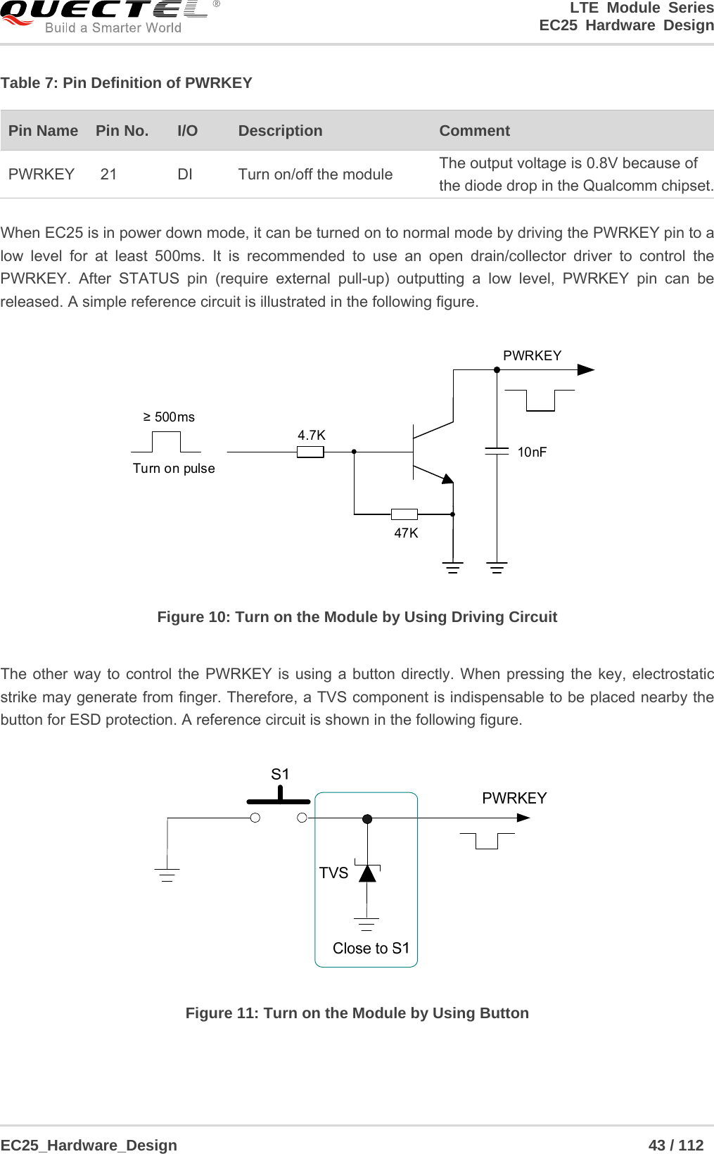
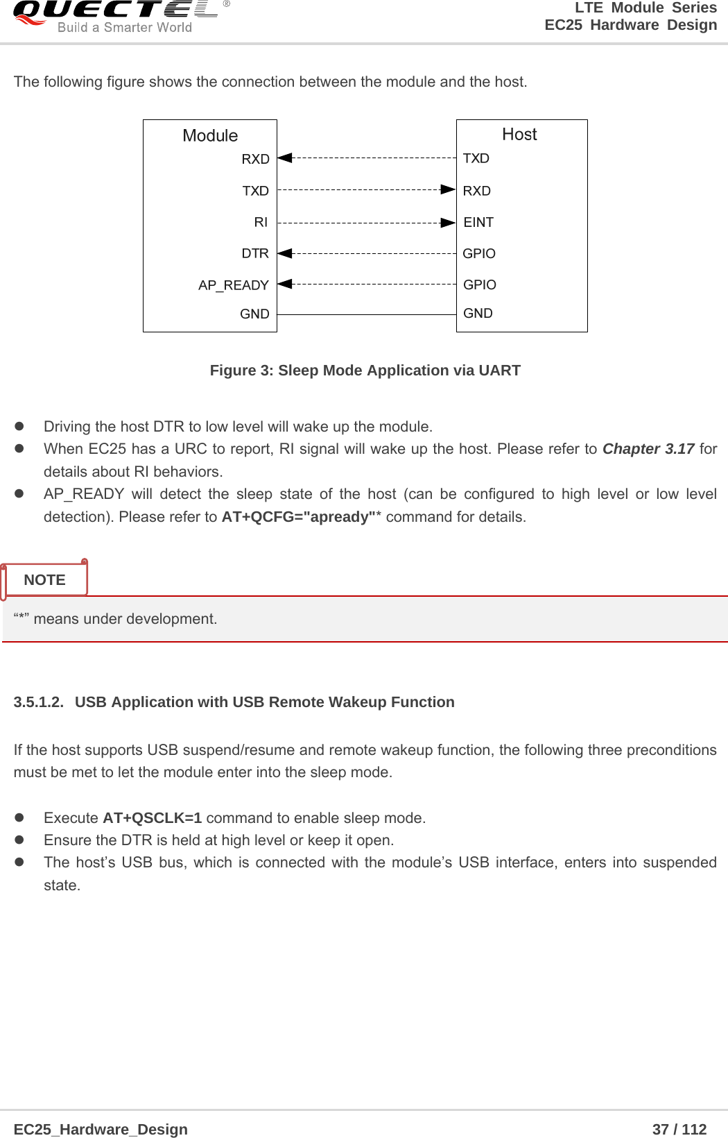
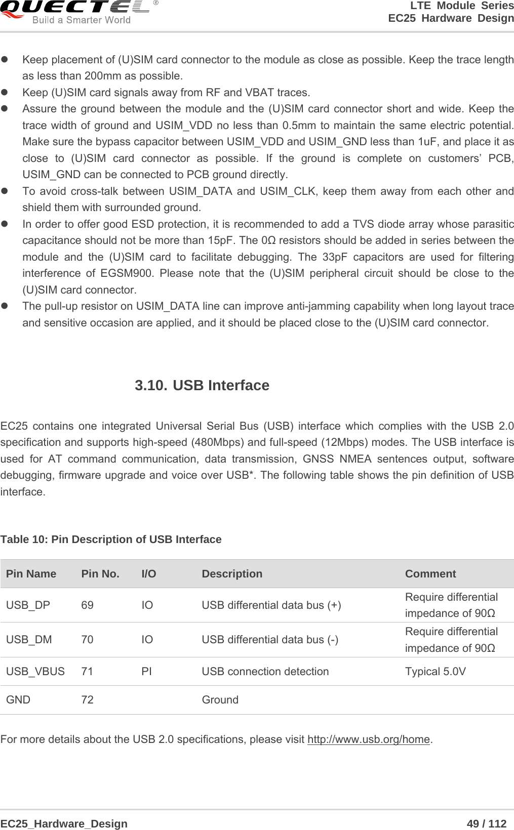
![LTE Module Series EC25 Hardware Design EC25_Hardware_Design 45 / 112 Figure 13: Timing of Turning off Module 3.7.2.2. Turn off Module Using AT Command It is also a safe way to use AT+QPOWD command to turn off the module, which is similar to turning off the module via PWRKEY pin. Please refer to document [2] for details about AT+QPOWD command. 1. Inorder to avoid damaging internal flash, please do not switch off the power supply when the module works normally. Only after the module is shut down by PWRKEY or AT command, then the power supply can be cut off. 2. When turn off module with AT command, please keep PWRKEY at high level after the execution of power-off command. Otherwise the module will be turned on again after successfully turn-off. 3.8. Reset the Module The RESET_N pin can be used to reset the module. The module can be reset by driving RESET_N to a low level voltage for time between 150ms and 460ms. Table 8: RESET_N Pin Description Pin Name Pin No. I/O Description Comment RESET_N 20 DI Reset the module 1.8V power domain NOTES](https://usermanual.wiki/Quectel-Wireless-Solutions/201805EC25AU.Users-Manual/User-Guide-3839081-Page-46.png)
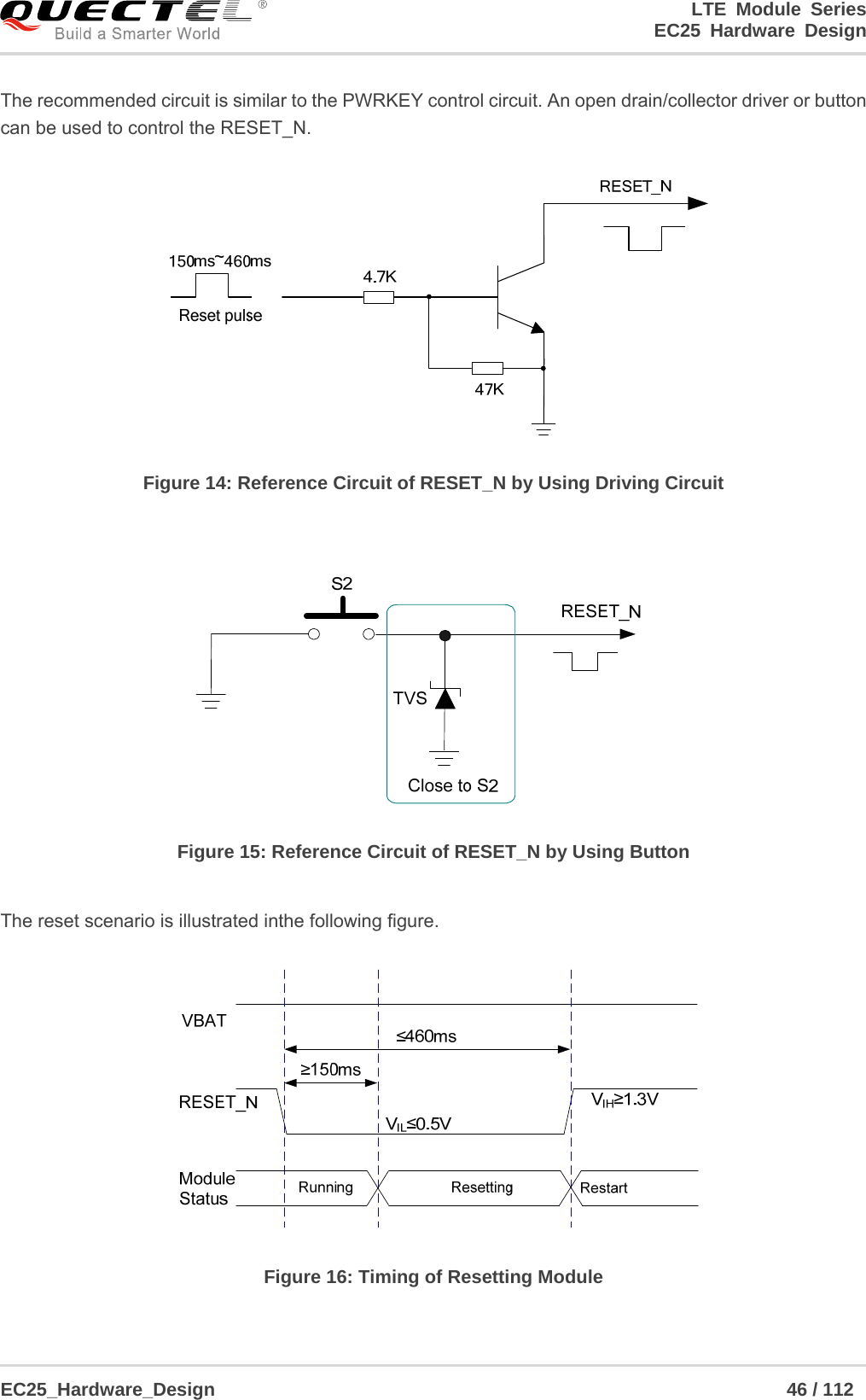
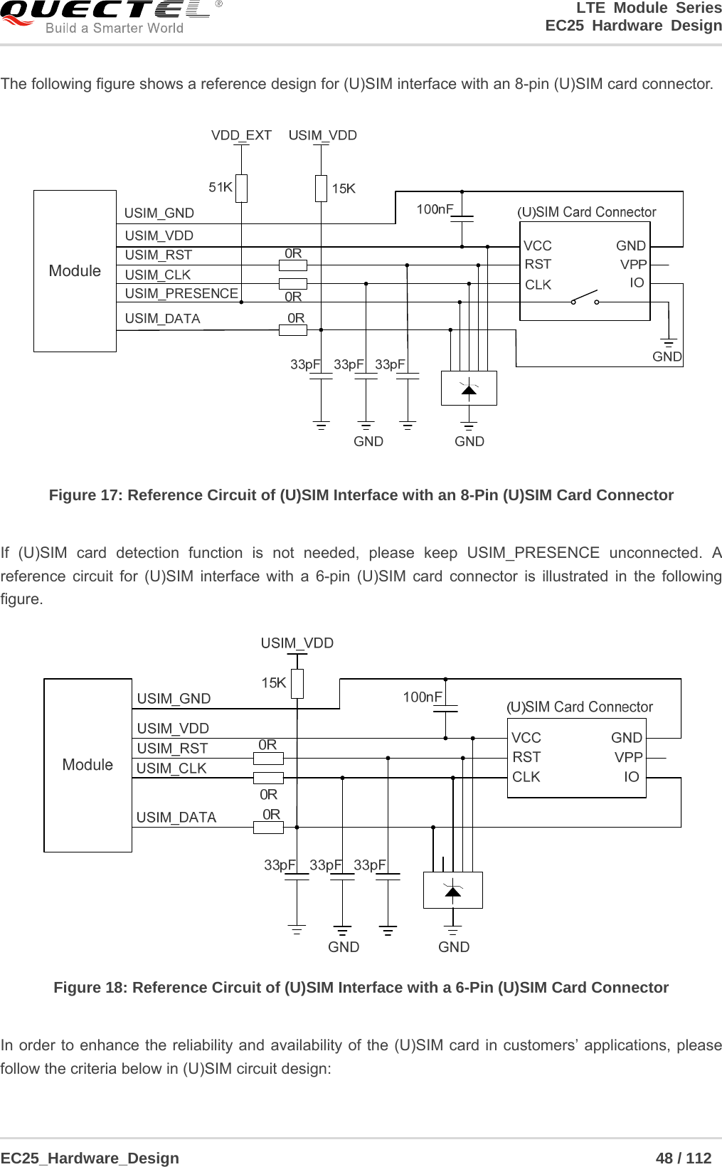
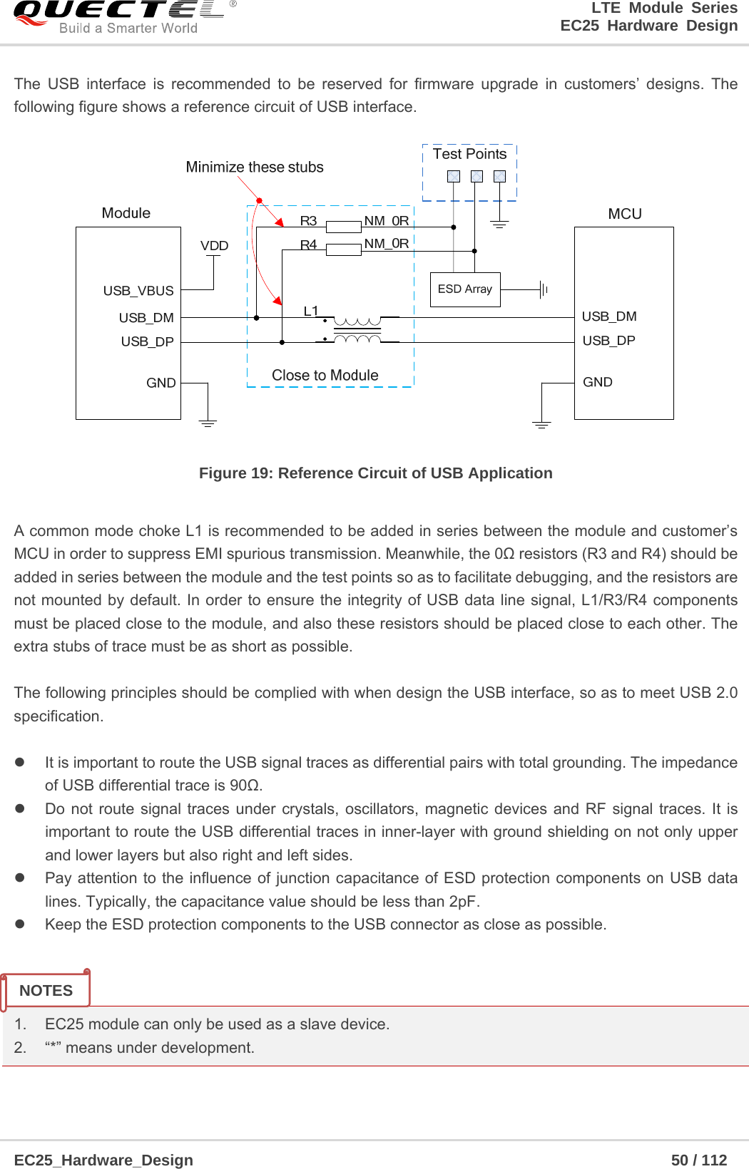
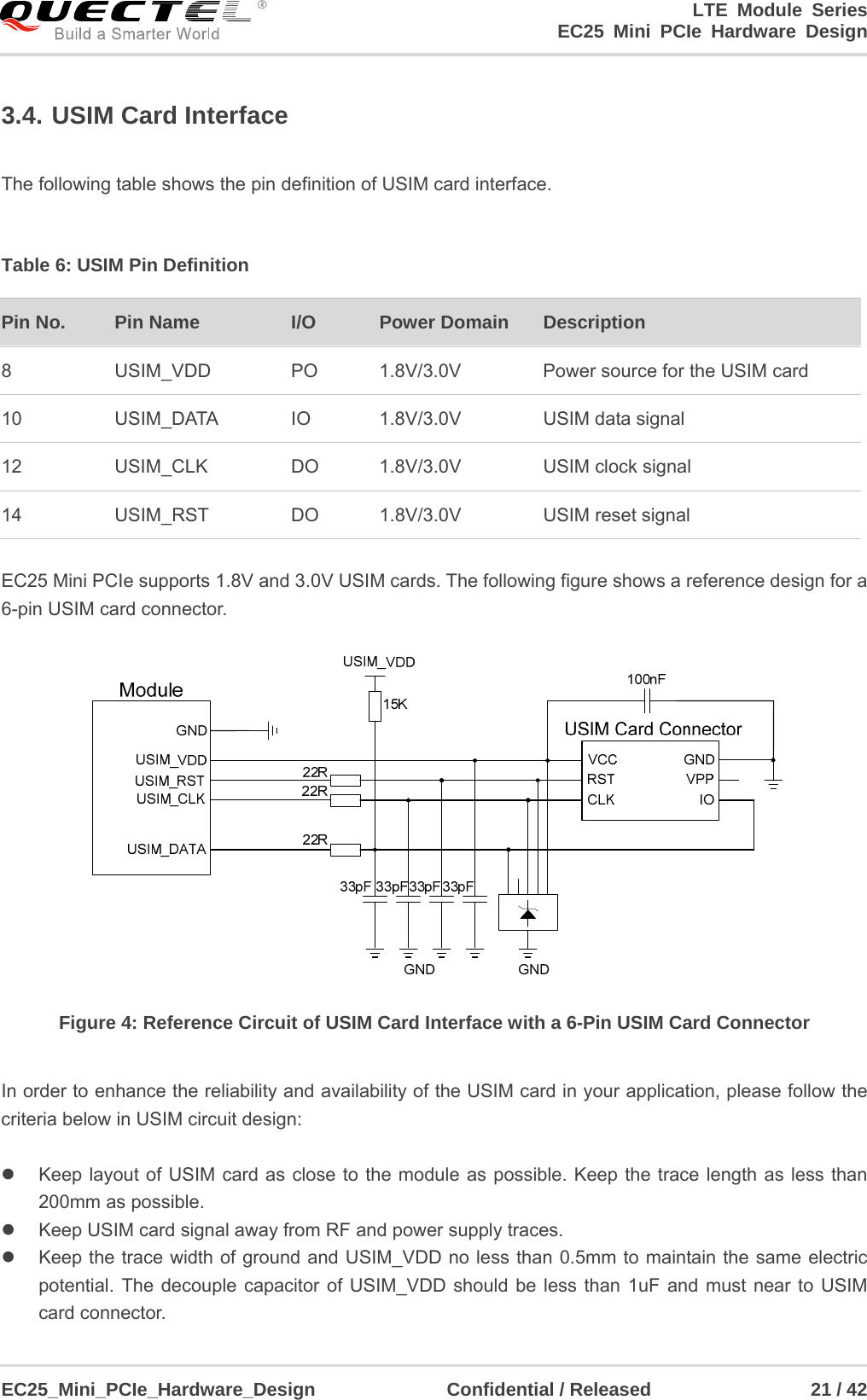
![LTE Module Series EC25 Hardware Design EC25_Hardware_Design 47 / 112 1. Use RESET_N only when turning off the module by AT+QPOWD command and PWRKEY pin failed. 2. Ensure that there is no large capacitance on PWRKEY and RESET_N pins. 3.9. (U)SIM Interface The(U)SIM interface circuitry meets ETSI and IMT-2000 requirements. Both 1.8V and 3.0V (U)SIM cards are supported. Table 9: Pin Definition of the (U)SIM Interface EC25 supports (U)SIM card hot-plug via the USIM_PRESENCE pin. The function supports low level and high level detections, and it is disabled by default. Please refer to document [2] for more details about AT+QSIMDET command. Pin Name Pin No. I/O Description Comment USIM_VDD 14 PO Power supply for (U)SIM card Either 1.8V or 3.0V is supported by the module automatically. USIM_DATA 15 IO Data signal of (U)SIM card USIM_CLK 16 DO Clock signal of (U)SIM card USIM_RST 17 DO Reset signal of (U)SIM card USIM_ PRESENCE 13 DI (U)SIM card insertion detection USIM_GND 10 Specified ground for (U)SIM card NOTES](https://usermanual.wiki/Quectel-Wireless-Solutions/201805EC25AU.Users-Manual/User-Guide-3839081-Page-48.png)
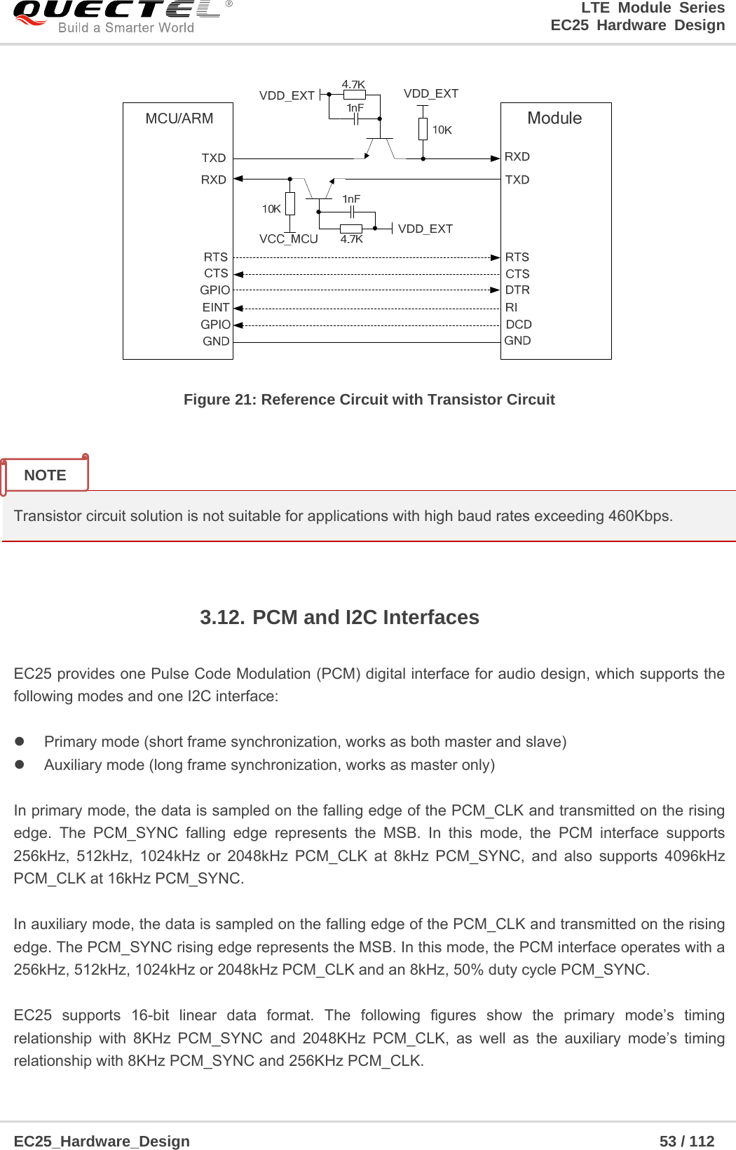
![LTE Module Series EC25 Hardware Design EC25_Hardware_Design 55 / 112 Clock and mode can be configured by AT command, and the default configuration is master mode using short frame synchronization format with 2048KHz PCM_CLK and 8KHz PCM_SYNC. Please refer to document [2] for more details about AT+QDAI command. The following figure shows a reference design of PCM interface with external codec IC. Figure 24: Reference Circuit of PCM Application with Audio Codec 1. It is recommended to reserve an RC (R=22Ω, C=22pF) circuits on the PCM lines, especially for PCM_CLK. 2. EC25 works as a master device pertaining to I2C interface. PCM_OUT 25 DO PCM data output 1.8V power domain PCM_SYNC 26 IO PCM data frame synchronization signal 1.8V power domain PCM_CLK 27 IO PCM data bit clock 1.8V power domain I2C_SCL 41 OD I2C serial clock Require external pull-up to 1.8V I2C_SDA 42 OD I2C serial data Require external pull-up to 1.8V NOTES](https://usermanual.wiki/Quectel-Wireless-Solutions/201805EC25AU.Users-Manual/User-Guide-3839081-Page-56.png)
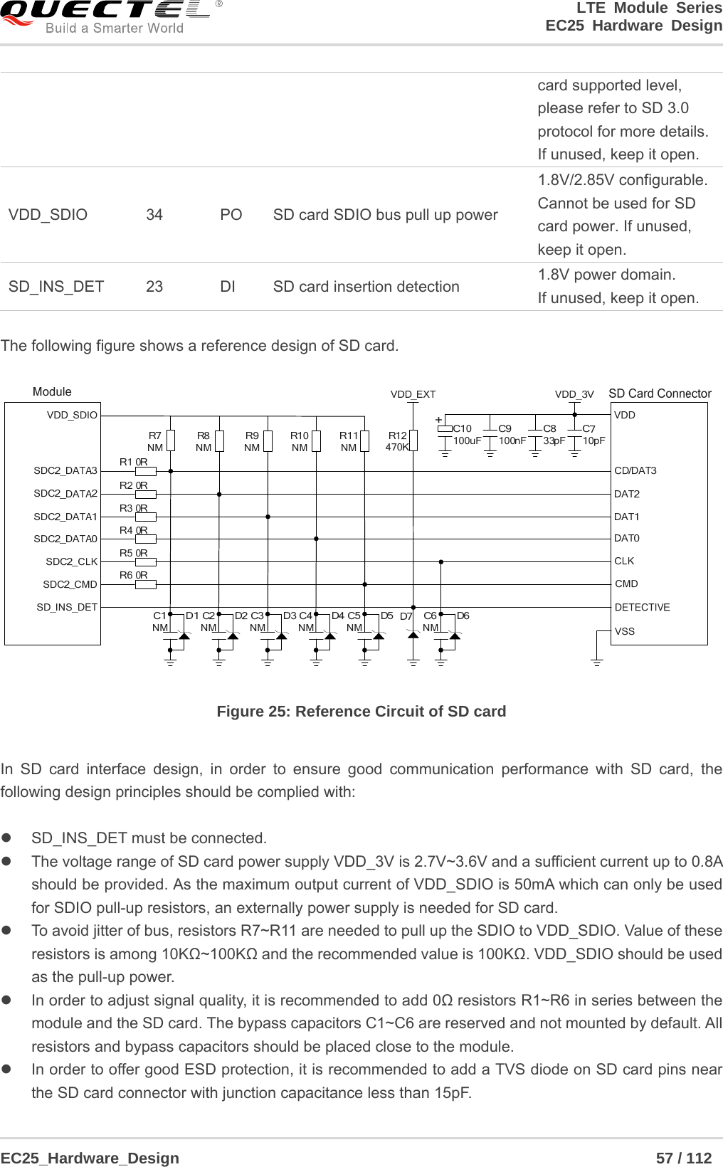
![LTE Module Series EC25 Hardware Design EC25_Hardware_Design 58 / 112 Keep SDIO signals far away from other sensitive circuits/signals such as RF circuits, analog signals, etc., as well as noisy signals such as clock signals, DCDC signals, etc. It is important to route the SDIO signal traces with total grounding. The impedance of SDIO data trace is 50Ω (±10%). Make sure the adjacent trace spacing is two times of the trace width and the load capacitance of SDIO bus should be less than 15pF. It is recommended to keep the trace length difference between CLK and DATA/CMD less than 1mm and the total routing length less than 50mm. The total trace length inside the module is 27mm, so the exterior total trace length should be less than 23mm. 3.14. ADC Interfaces The module provides two analog-to-digital converter (ADC) interfaces. AT+QADC=0 command can be used to read the voltage value on ADC0 pin. AT+QADC=1 command can be used to read the voltage value on ADC1 pin. For more details about these AT commands, please refer to document [2]. In order to improve the accuracy of ADC, the trace of ADC should be surrounded by ground. Table 16: Pin Definition of ADC Interfaces The following table describes the characteristic of ADC function. Table 17: Characteristic of ADC Pin Name Pin No. Description ADC0 45 General purpose analog to digital converter ADC1 44 General purpose analog to digital converter Parameter Min. Typ. Max. Unit ADC0 Voltage Range 0.3 VBAT_BB V ADC1 Voltage Range 0.3 VBAT_BB V ADC Resolution 15 Bits](https://usermanual.wiki/Quectel-Wireless-Solutions/201805EC25AU.Users-Manual/User-Guide-3839081-Page-59.png)
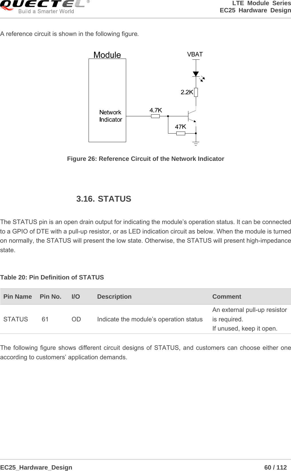
![LTE Module Series EC25 Hardware Design EC25_Hardware_Design 61 / 112 Figure 27: Reference Circuits of STATUS 3.17. Behaviors of RI AT+QCFG="risignaltype","physical" command can be used to configure RI behavior. No matter on which port URC is presented, URC will trigger the behavior of RI pin. URC can be outputted from UART port, USB AT port and USB modem port through configuration via AT+QURCCFG command. The default port is USB AT port. In addition, RI behavior can be configured flexibly. The default behavior of the RI is shown as below. Table 21: Behavior of RI The RI behavior can be changed by AT+QCFG="urc/ri/ring" command. Please refer to document [2] for details. State Response Idle RI keeps at high level URC RI outputs 120ms low pulse when a new URC returns NOTE](https://usermanual.wiki/Quectel-Wireless-Solutions/201805EC25AU.Users-Manual/User-Guide-3839081-Page-62.png)
![LTE Module Series EC25 Hardware Design EC25_Hardware_Design 65 / 112 The following figure shows a reference design of wireless connectivity interfaces with Quectel FC20 module. ModuleWAKE_ ON_WIRELESSWLAN_SL P_CLKPM_ENAB LEDCDC/LDO32K HZ_I NWAKE_ ON_WIRELE SSFC20 ModuleVDD_3V3POWERSDC1_DATA3SDC1_DATA2SDC1_DATA1SDC1_DATA0SDC1_CLKSDC1_CMDWLAN_ENSDIO_D3SDIO_D2SDIO_D1SDIO_D0SDIO_CLKSDIO_CMDWLAN_ENWLANVDD_EXT VIOCOEX_UART_TXCOEX_ UART_RX LTE_UART_TXDLTE_UART_RXDCOEX Figure 30: Reference Circuit of Wireless Connectivity Interfaces with FC20 Module 1. FC20 module can only be used as a slave device. 2. When BT function is enabled on EC25 module, PCM_SYNC and PCM_CLK pins are only used to output signals. 3. For more information about wireless connectivity interfaces, please refer to document [5]. BT_RXD* 39 DI BT UART receive data 1.8V power domain BT_CTS* 40 DO BT UART clear to send 1.8V power domain. Cannot be pulled up before startup. PCM_IN1) 24 DI PCM data input 1.8V power domain PCM_OUT1) 25 DO PCM data output 1.8V power domain PCM_SYNC1) 26 IO PCM data frame synchronization signal 1.8V power domain PCM_CLK1) 27 IO PCM data bit clock 1.8V power domain BT_EN* 139 DO BT function control via BT module. 1.8V power domain Active high. NOTES](https://usermanual.wiki/Quectel-Wireless-Solutions/201805EC25AU.Users-Manual/User-Guide-3839081-Page-66.png)
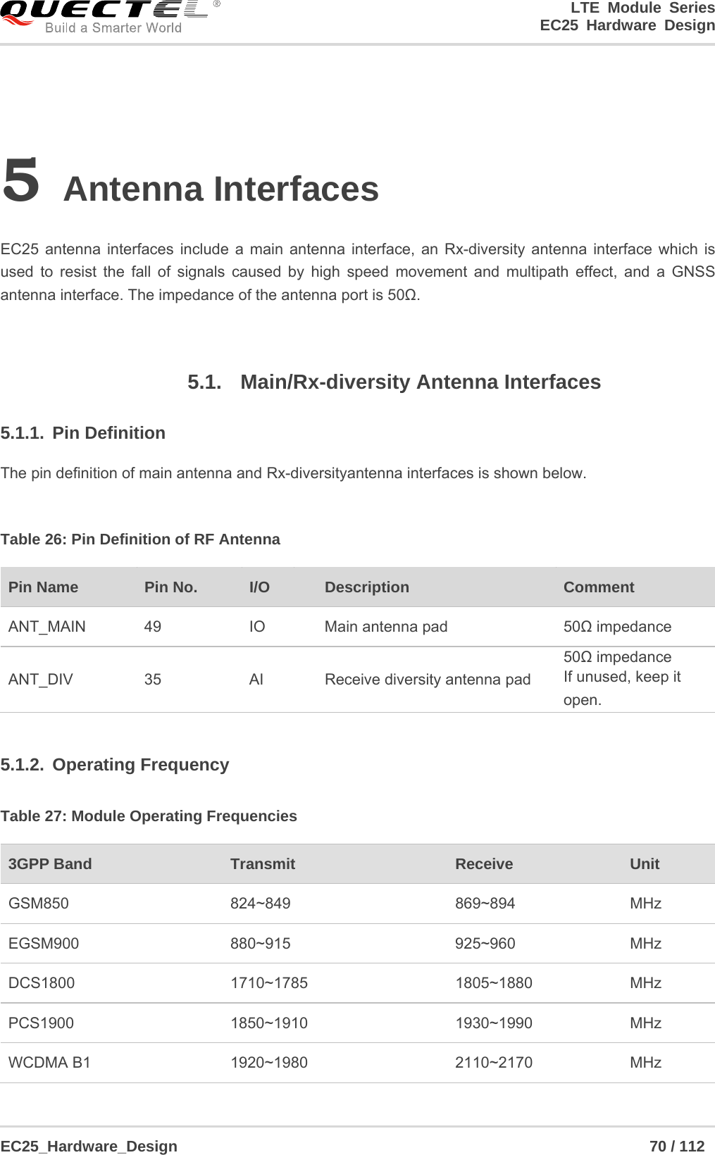
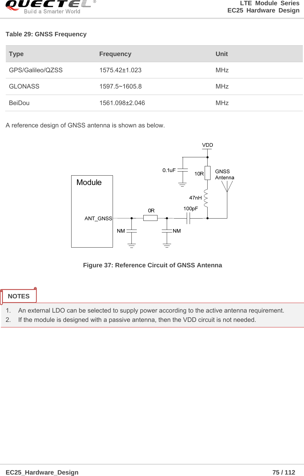
![LTE Module Series EC25 Hardware Design EC25_Hardware_Design 68 / 112 4 GNSS Receiver 4.1. General Description EC25 includes a fully integrated global navigation satellite system solution that supports Gen8C-Lite of Qualcomm (GPS, GLONASS, BeiDou, Galileo and QZSS). EC25 supports standard NMEA-0183 protocol, and outputs NMEA sentences at 1Hz data update rate via USB interface by default. By default, EC25 GNSS engine is switched off. It has to be switched on via AT command. For more details about GNSS engine technology and configurations, please refer to document [3]. 4.2. GNSS Performance The following table shows GNSS performance of EC25. Table 25: GNSS Performance Parameter Description Conditions Typ. Unit Sensitivity (GNSS) Cold start Autonomous -146 dBm Reacquisition Autonomous -157 dBm Tracking Autonomous -157 dBm TTFF (GNSS) Cold start @open sky Autonomous 35 s XTRA enabled 18 s Warm start @open sky Autonomous 26 s XTRA enabled 2.2 s](https://usermanual.wiki/Quectel-Wireless-Solutions/201805EC25AU.Users-Manual/User-Guide-3839081-Page-69.png)
![LTE Module Series EC25 Hardware Design EC25_Hardware_Design 74 / 112 Figure 36: Coplanar Waveguide Line Design on a 4-layer PCB (Layer 4 as Reference Ground) In order to ensure RF performance and reliability, the following principles should be complied with in RF layout design: Please use an impedance simulation tool to control the characteristic impedance of RF traces as 50Ω. The GND pins adjacent to RF pins should not be designed as thermal relief pads, and they should be fully connected to ground. The distance between the RF pins and the RF connector should be as short as possible, and all the right angle traces should be changed to curved ones. There should be clearance area under the signal pin of the antenna connector or solder joint. The reference ground of RF traces should be complete. Meanwhile, adding some ground vias around RF traces and the reference ground could help to improve RF performance. The distance between the ground vias and RF traces should be no less than two times the width of RF signal traces (2*W). For more details about RF layout, please refer to document [6]. 5.2. GNSS Antenna Interface The following tables show pin definition and frequency specification of GNSS antenna interface. Table 28: Pin Definition of GNSS Antenna Interface Pin Name Pin No. I/O Description Comment ANT_GNSS 47 AI GNSS antenna 50Ω impedance If unused, keep it open.](https://usermanual.wiki/Quectel-Wireless-Solutions/201805EC25AU.Users-Manual/User-Guide-3839081-Page-75.png)
![LTE Module Series EC25 Hardware Design EC25_Hardware_Design 105 / 112 8.2. Manufacturing and Soldering Push the squeegee to apply the solder paste on the surface of stencil, thus making the paste fill the stencil openings and then penetrate to the PCB. The force on the squeegee should be adjusted properlyso as to produce a clean stencil surface on a single pass. To ensure the module soldering quality, thethickness of stencil for the module is recommended to be 0.20mm. For more details, please refer to document [4]. It is suggested that the peak reflow temperature is 235ºC~245ºC (for SnAg3.0Cu0.5 alloy). The absolute maximum reflow temperature is 260ºC. To avoid damage to the module caused by repeated heating, it is suggested that the module should be mounted after reflow soldering for the other side of PCB has been completed. Recommended reflow soldering thermal profile is shown below: Figure 48: Reflow Soldering Thermal Profile](https://usermanual.wiki/Quectel-Wireless-Solutions/201805EC25AU.Users-Manual/User-Guide-3839081-Page-106.png)
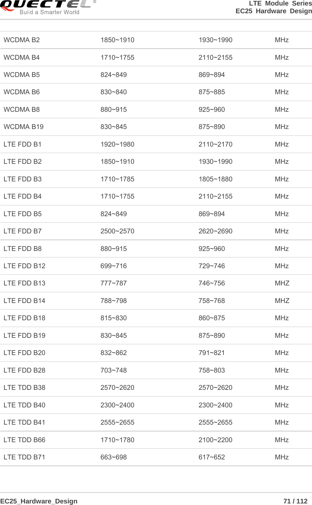
![LTE Module Series EC25 Hardware Design EC25_Hardware_Design 107 / 112 9 Appendix A References Table 52: Related Documents Table 53: Terms and Abbreviations SN Document Name Remark [1] Quectel_EC2x&EG9x&EM05_Power_Management_Application_Note Power management application notefor EC25, EC21, EC20 R2.0, EC20 R2.1, EG95, EG91 and EM05 modules [2] Quectel_EC25&EC21_AT_Commands_Manual EC25 and EC21 AT commands manual[3] Quectel_EC25&EC21_GNSS_AT_Commands_ Manual EC25 and EC21 GNSS AT commands manual [4] Quectel_Module_Secondary_SMT_User_Guide Module secondary SMT user guide [5] Quectel_EC25_Reference_Design EC25 reference design [6] Quectel_RF_Layout_Application_Note RF layout application note Abbreviation Description AMR Adaptive Multi-rate bps Bits Per Second CHAP Challenge Handshake Authentication Protocol CS Coding Scheme CSD Circuit Switched Data CTS Clear To Send DC-HSPA+ Dual-carrier High Speed Packet Access DFOTA Delta Firmware Upgrade Over The Air](https://usermanual.wiki/Quectel-Wireless-Solutions/201805EC25AU.Users-Manual/User-Guide-3839081-Page-108.png)

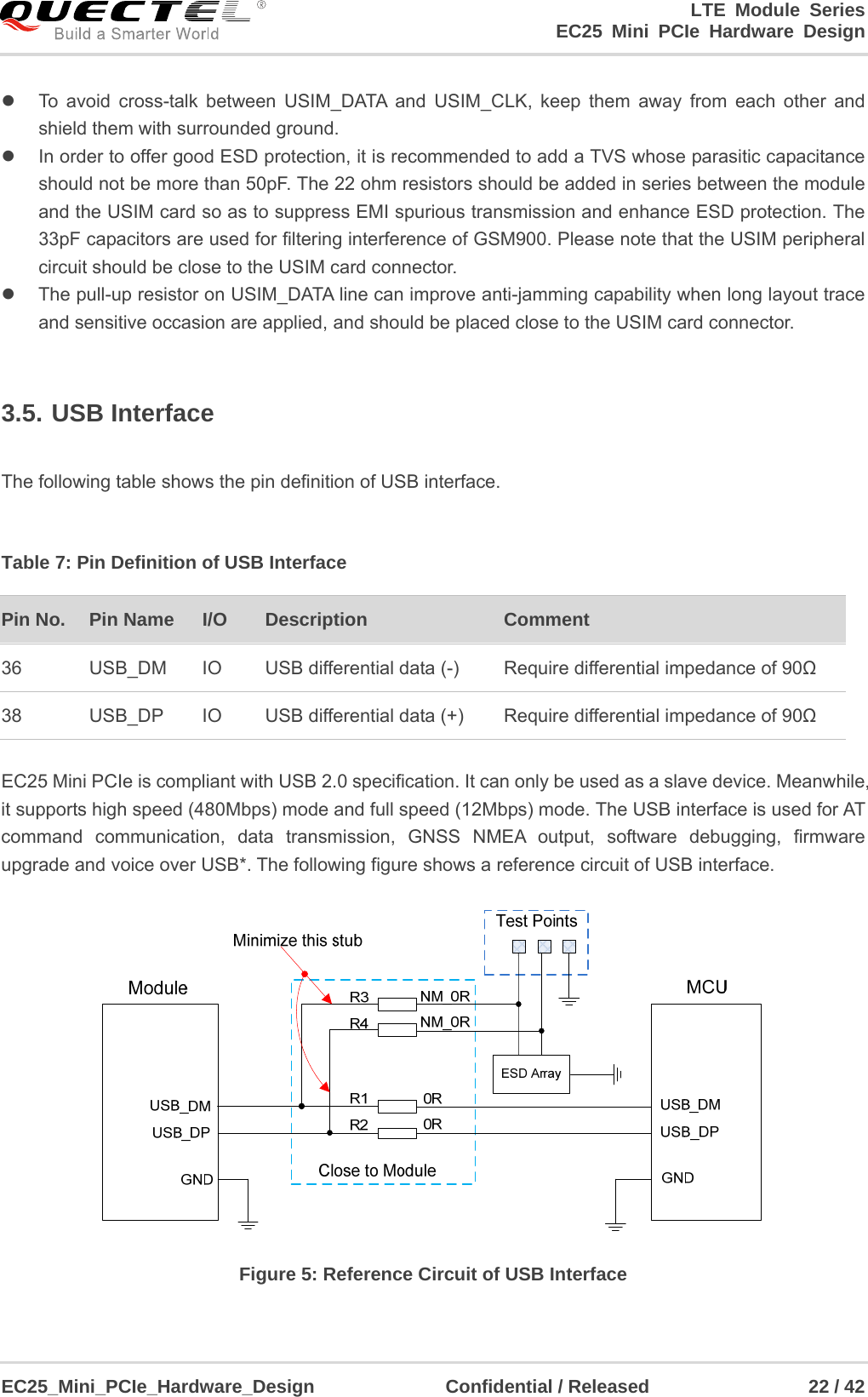
![LTE Module Series EC25 Mini PCIe Hardware Design EC25_Mini_PCIe_Hardware_Design Confidential / Released 23 / 42 In order to ensure the integrity of USB data line signal, components R1, R2, R3 and R4 must be placed close to the module, and also these resistors should be placed close to each other. The extra stubs of trace must be as short as possible. In order to ensure the USB interface design corresponding with the USB 2.0 specification, please comply with the following principles: It is important to route the USB signal traces as differential pairs with total grounding. The impedance of USB differential trace is 90 ohm. Do not route signal traces under crystals, oscillators, magnetic devices or RF signal traces. It is important to route the USB differential traces in inner-layer with ground shielding on not only upper and lower layers but also right and left sides. If USB connector is used, please keep the ESD protection components to the USB connector as close as possible. Pay attention to the influence of junction capacitance of ESD protection components on USB data lines. Typically, the capacitance value should be less than 2pF. Keep traces of USB data test points short to avoid noise coupled on USB data lines. If possible, reserve a 0R resistor on these two lines. 1. There are three preconditions when enabling EC25 Mini PCIe to enter into the sleep mode: a) Execute AT+QSCLK=1 command to enable the sleep mode. Please refer to document [2] for details. b) DTR pin should be kept in high level (pull-up internally). c) USB interface on Mini PCIe must be connected with the USB interface of the host and please guarantee the USB of the host is in suspended state. 2. “*” means under development. 3.6. UART Interface The following table shows the pin definition of the UART interface. Table 8: Pin Definition of the UART Interface Pin No. EC25 Mini PCIe Pin Name I/O Power Domain Description 11 UART_RX DI 3.3V UART receive data 13 UART_TX DO 3.3V UART transmit data 23 UART_CTS DI 3.3V UART clear to send 25 UART_RTS DO 3.3V UART request to send NOTES](https://usermanual.wiki/Quectel-Wireless-Solutions/201805EC25AU.Users-Manual/User-Guide-3839081-Page-139.png)
![LTE Module Series EC25 Mini PCIe Hardware Design EC25_Mini_PCIe_Hardware_Design Confidential / Released 24 / 42 The UART interface supports 9600, 19200, 38400, 57600, 115200 and 230400bps baud rate. The default is 115200bps. This interface can be used for AT command communication. AT+IPR command can be used to set the baud rate of the UART, and AT+IFC command can be used to set the hardware flow control (hardware flow control is disabled by default). Please refer to document [2] for details. 3.7. PCM and I2C Interfaces The following table shows the pin definition of PCM and 12C interfaces that can be applied in audio codec design. Table 9: Pin Definition of PCM and I2C Interfaces EC25 Mini PCIe provides one PCM digital interface, which supports 8-bit A-law* and μ-law*, and also supports 16-bit linear data formats and the following modes: Primary mode (short frame synchronization, works as either master or slave) Auxiliary mode (long frame synchronization, works as master only) “*” means under development. Pin No. Pin Name I/O Power Domain Description 45 PCM_CLK IO 1.8V PCM clock signal 47 PCM_DOUT DO 1.8V PCM data output 49 PCM_DIN DI 1.8V PCM data input 51 PCM_SYNC IO 1.8V PCM frame synchronization 30 I2C_SCL DO 1.8V I2C serial clock, require external pull-up to 1.8V. 32 I2C_SDA IO 1.8V I2C serial data, require external pull-up to 1.8V. NOTE NOTE](https://usermanual.wiki/Quectel-Wireless-Solutions/201805EC25AU.Users-Manual/User-Guide-3839081-Page-140.png)
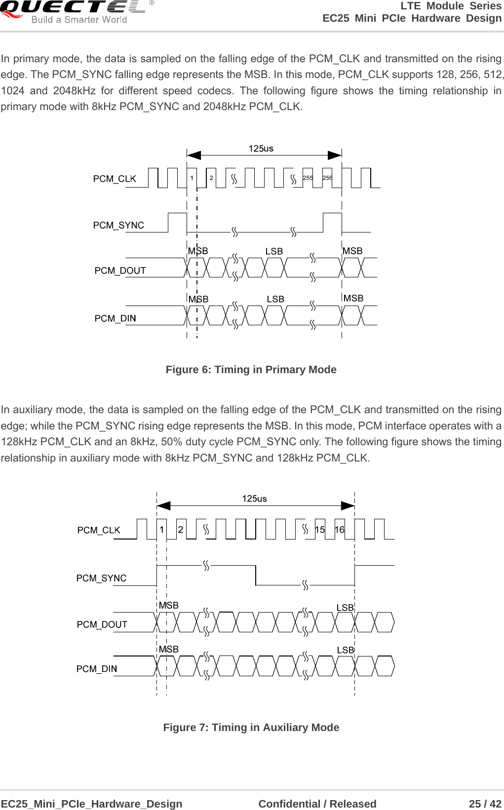
![LTE Module Series EC25 Mini PCIe Hardware Design EC25_Mini_PCIe_Hardware_Design Confidential / Released 26 / 42 Clock and mode can be configured by AT command, and the default configuration is master mode using short frame synchronization format with 2048kHz PCM_CLK and 8kHz PCM_SYNC. In addition, EC25 Mini PCIe’s firmware has integrated the configuration on some PCM codec’s application with I2C interface. Please refer to document [2] for details about AT+QDAI command. The following figure shows a reference design of PCM interface with an external codec IC. Figure 8: Reference Circuit of PCM Application with Audio Codec 3.8. Control Signals The following table shows the pin definition of control signals. Table 10: Pin Definition of Control Signals Pin No. Pin Name I/O Power Domain Description 17 RI DO 3.3V Output signal can be used to wake up the host. 31 DTR DI 3.3V Sleep mode control 20 W_DISABLE# DI 3.3V Disable wireless communications; pull-up by default, active low. 22 PERST# DI 3.3V Functional reset to the card; active low. 42 LED_WWAN# OC Active-low. LED signal for indicating the state of the module. 1 WAKE# OC Output signal can be used to wake up the host.](https://usermanual.wiki/Quectel-Wireless-Solutions/201805EC25AU.Users-Manual/User-Guide-3839081-Page-142.png)
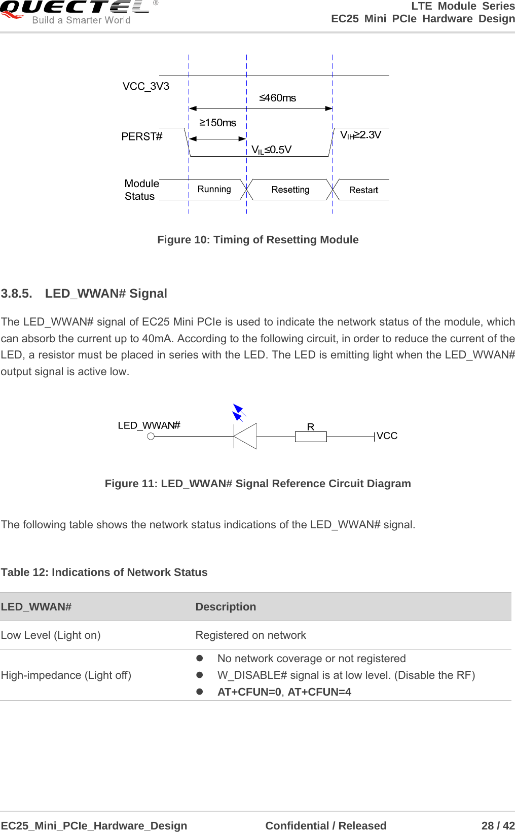
![LTE Module Series EC25 Mini PCIe Hardware Design EC25_Mini_PCIe_Hardware_Design Confidential / Released 27 / 42 3.8.1. RI Signal The RI signal can be used to wake up the host. When URC returns, there will be the following behavior on the RI pin after executing AT+QCFG=“risignaltype”,“physical” command. Figure 9: RI Behavior 3.8.2. DTR Signal The DTR signal supports sleep control function. Driving it to low level will wake up the module. 3.8.3. W_DISABLE# Signal EC25 Mini PCIe provides W_DISABLE# signal to disable wireless communications through hardware operation. The following table shows the radio operational states of the module. Please refer to document [2] for related AT commands. Table 11: Radio Operational States 3.8.4. PERST# Signal The PERST# signal can be used to force a hardware reset on the card. You can reset the module by driving the PERST# to a low level voltage with the time frame of 150~460ms and then releasing it. The reset scenario is illustrated in the following figure. W_DISABLE# AT Commands Radio Operation High Level AT+CFUN=1 Enabled High Level AT+CFUN=0 AT+CFUN=4 Disabled Low Level AT+CFUN=0 AT+CFUN=1 AT+CFUN=4 Disabled](https://usermanual.wiki/Quectel-Wireless-Solutions/201805EC25AU.Users-Manual/User-Guide-3839081-Page-143.png)
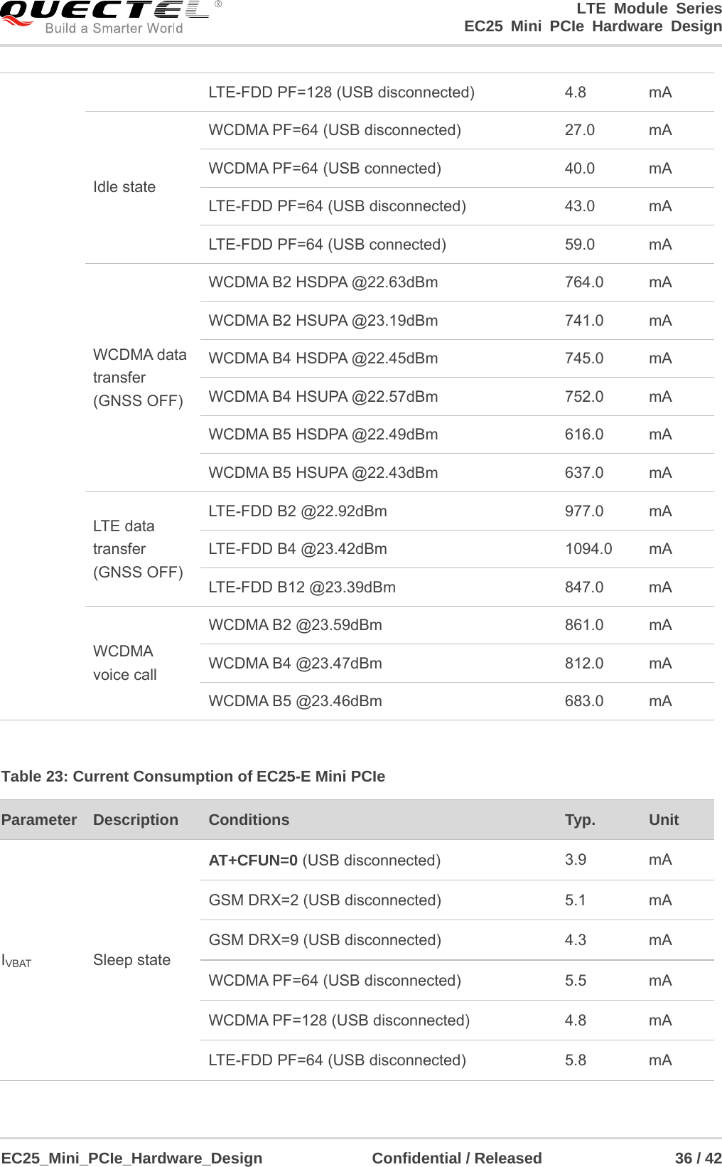
![LTE Module Series EC25 Mini PCIe Hardware Design EC25_Mini_PCIe_Hardware_Design Confidential / Released 35 / 42 XTRA file contains predicted GPS and GLONASS satellites coordinates and clock biases valid for up to 7 days. It is best if XTRA file is downloaded every 1-2 days. Additionally, EC25 Mini PCIe can support standard NMEA-0183 protocol and output NMEA messages with 1Hz via USB NMEA interface. EC25 Mini PCIe GNSS engine is switched off by default. You must switch on it by AT command. Please refer to document [3] for more details about GNSS engine technology and configurations. A passive antenna should be used for the GNSS engine. 4.6. ESD Characteristics The following table shows the ESD characteristics of EC25 Mini PCIe. Table 21: ESD Characteristics of EC25 Mini PCIe 4.7. Current Consumption The following tables describe the current consumption of EC25 Mini PCIe series module. Table 22: Current Consumption of EC25-A Mini PCIe Parameter Description Conditions Typ. Unit IVBAT Sleep state AT+CFUN=0 (USB disconnected) 3.6 mA WCDMA PF=64 (USB disconnected) 4.4 mA WCDMA PF=128 (USB disconnected) 3.8 mA LTE-FDD PF=64 (USB disconnected) 5.9 mA Part Contact Discharge Air Discharge Unit Power Supply and GND +/-5 +/-10 kV Antenna Interface +/-4 +/-8 kV USB Interface +/-4 +/-8 kV USIM Interface +/-4 +/-8 kV Others +/-0.5 +/-1 kV](https://usermanual.wiki/Quectel-Wireless-Solutions/201805EC25AU.Users-Manual/User-Guide-3839081-Page-151.png)

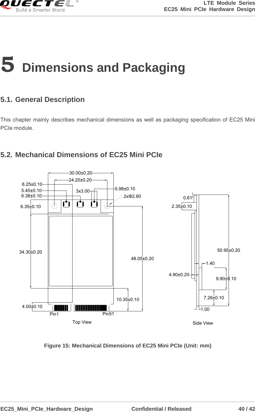
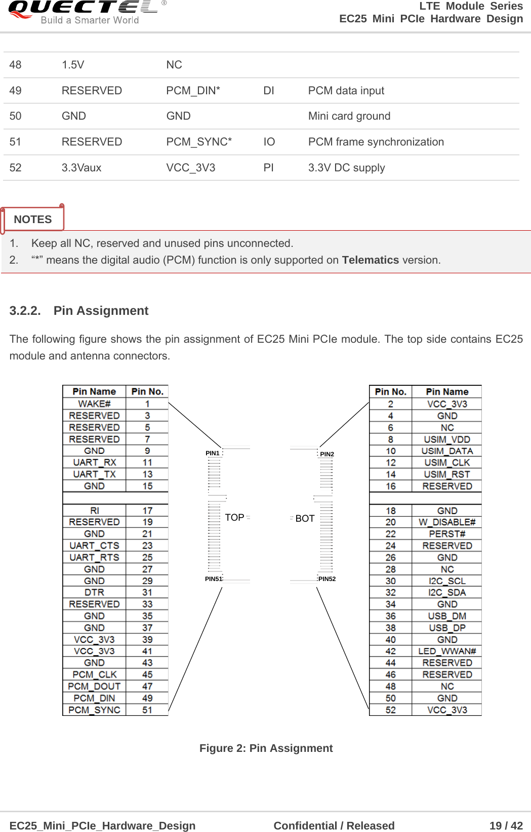
![LTE Module Series EC25 Mini PCIe Hardware Design EC25_Mini_PCIe_Hardware_Design Confidential / Released 41 / 42 5.3. Standard Dimensions of Mini PCI Express The following figure shows the standard dimensions of Mini PCI Express. Please refer to document [1] for detailed A and B. Figure 16: Standard Dimensions of Mini PCI Express (Unit: mm)](https://usermanual.wiki/Quectel-Wireless-Solutions/201805EC25AU.Users-Manual/User-Guide-3839081-Page-157.png)
![LTE Module Series EC25 Mini PCIe Hardware Design EC25_Mini_PCIe_Hardware_Design Confidential / Released 42 / 42 EC25 Mini PCIe adopts a standard Mini PCI Express connector which compiles with the directives and standards listed in the document [1]. The following figure takes the Molex 679100002 as an example. Figure 17: Dimensions of the Mini PCI Express Connector (Molex 679100002, Unit: mm) 5.4. Packaging Specification The EC25 Mini PCIe is packaged in a tray. Each tray contains 10pcs of modules. The smallest package of EC25 Mini PCIe contains 100pcs.](https://usermanual.wiki/Quectel-Wireless-Solutions/201805EC25AU.Users-Manual/User-Guide-3839081-Page-158.png)
![LTE Module Series EC25 Mini PCIe Hardware Design EC25_Mini_PCIe_Hardware_Design Confidential / Released 43 / 42 6 Appendix References Table 26: Related Documents Table 27: Terms and Abbreviations SN Document Name Remark [1] PCI Express Mini Card Electromechanical Specification Revision 1.2 Mini PCI Express Specification [2] Quectel_EC25&EC21_AT_Commands_Manual EC25 and EC21 AT Commands Manual [3] Quectel_EC25&EC21_GNSS_AT_Commands_ Manual EC25 and EC21 GNSS AT Commands Manual Abbreviation Description AMR Adaptive Multi-rate bps Bits Per Second CS Coding Scheme DC-HSPA+ Dual-carrier High Speed Packet Access DFOTA Delta Firmware Upgrade Over The Air DL Down Link EFR Enhanced Full Rate ESD Electrostatic Discharge FDD Frequency Division Duplexing FR Full Rate GLONASS GLObalnaya Navigatsionnaya Sputnikovaya Sistema, the Russian Global Navigation Satellite System GMSK Gaussian Minimum Shift Keying](https://usermanual.wiki/Quectel-Wireless-Solutions/201805EC25AU.Users-Manual/User-Guide-3839081-Page-159.png)