Quectel Wireless Solutions 201805EC25AU LTE Module User Manual
Quectel Wireless Solutions Company Limited LTE Module Users Manual
Contents
- 1. Users Manual
- 2. User Manual
Users Manual

EC25 Hardware Design
LTE Module Series
Rev. EC25_Hardware_Design_V1.5
Date: 2018-04-20
Status: Released
www.quectel.com

LTE Module Series
EC25 Hardware Design
EC25_Hardware_Design 1 / 112
Our aim is to provide customers with timely and comprehensive service. For any
assistance, please contact our company headquarters:
Quectel Wireless Solutions Co., Ltd.
7th Floor, Hongye Building, No.1801 Hongmei Road, Xuhui District, Shanghai 200233, China
Tel: +86 21 5108 6236
Email: info@quectel.com
Or our local office. For more information, please visit:
http://quectel.com/support/sales.htm
For technical support, or to report documentation errors, please visit:
http://quectel.com/support/technical.htm
Or Email to: support@quectel.com
GENERAL NOTES
QUECTEL OFFERS THE INFORMATION AS A SERVICE TO ITS CUSTOMERS. THE INFORMATION
PROVIDED IS BASED UPON CUSTOMERS’ REQUIREMENTS. QUECTEL MAKES EVERY EFFORT
TO ENSURE THE QUALITY OF THE INFORMATION IT MAKES AVAILABLE. QUECTEL DOES NOT
MAKE ANY WARRANTY AS TO THE INFORMATION CONTAINED HEREIN, AND DOES NOT ACCEPT
ANY LIABILITY FOR ANY INJURY, LOSS OR DAMAGE OF ANY KIND INCURRED BY USE OF OR
RELIANCE UPON THE INFORMATION. ALL INFORMATION SUPPLIED HEREIN IS SUBJECT TO
CHANGE WITHOUT PRIOR NOTICE.
COPYRIGHT
THE INFORMATION CONTAINED HERE IS PROPRIETARY TECHNICAL INFORMATION OF
QUECTEL WIRELESS SOLUTIONS CO., LTD. TRANSMITTING, REPRODUCTION, DISSEMINATION
AND EDITING OF THIS DOCUMENT AS WELL AS UTILIZATION OF THE CONTENT ARE
FORBIDDEN WITHOUT PERMISSION. OFFENDERS WILL BE HELD LIABLE FOR PAYMENT OF
DAMAGES. ALL RIGHTS ARE RESERVED IN THE EVENT OF A PATENT GRANT OR
REGISTRATION OF A UTILITY MODEL OR DESIGN.
Copyright © Quectel Wireless Solutions Co., Ltd. 2018. All rights reserved.

LTE Module Series
EC25 Hardware Design
EC25_Hardware_Design 2 / 112
About the Document
History
Revision Date Author Description
1.0 2016-04-01 Woody WU Initial
1.1 2016-09-22
Lyndon LIU/
Frank WANG
1. Updated EC25 series frequency bands in Table 1.
2. Updated transmitting power, supported maximum
baud rate of main UART/internal protocols/USB
drivers of USB interface, firmware upgrade and
temperature range in Table 2.
3. Updated timing of turning on module in Figure 12.
4. Updated timing of turning off module in Figure 13.
5. Updated timing of resetting module in Figure 16.
6. Updated supported baud rates of main UART in
Chapter 3.11.
7. Added notes for ADC interface in Chapter 3.13.
8. Updated GNSS performance in Table 21.
9. Updated operating frequencies of module in Table 23.
10. Added current consumption in Chapter 6.4.
11. Updated RF output power in Chapter 6.5.
12. Added RF receiving sensitivity in Chapter 6.6.
1.2 2016-11-04
Lyndon LIU/
Michael ZHANG
1. Added SGMII and WLAN interfaces in Table 2.
2. Updated function diagram in Figure 1.
3. Updated pin assignment (Top View) in Figure 2.
4. Added description of SGMII and WLAN interfaces in
Table 4.
5. Added SGMII interface in Chapter 3.17.
6. Added WLAN interface in Chapter 3.18.
7. Added USB_BOOT interface in Chapter 3.19.
8. Added reference design of RF layout in Chapter 5.1.4.
9. Added note about SIMO in Chapter 6.6.
1.3 2017-01-24
Lyndon LIU/
Frank WANG
1. Updated function diagram in Figure 1.
2. Updated pin assignment (top view) in Figure 2.

LTE Module Series
EC25 Hardware Design
EC25_Hardware_Design 3 / 112
3. Added BT interface in Chapter 3.18.2.
4. Updated GNSS performance in Table 24.
5. Updated reference circuit of wireless connectivity
interfaces with FC20 module in Figure 29.
6. Updated current consumption of EC25-E module in
Table 33.
7. Updated EC25-A conducted RF receiving sensitivity
in Table 38.
8. AddedEC25-J conducted RF receiving sensitivity in
Table 40.
1.4 2018-03-05
AnniceZHANG/
Lyndon LIU/
Frank WANG
1. Updated functional diagram in Figure 1.
2. Updated frequency bands in Table 1.
3. Updated LTE, UMTS and GSM features in Table 2.
4. Updated description of pin 40/136/137/138.
5. Updated PWRKEY pulled down time to 500ms in
Chapter 3.7.1 and reference circuit in Figure 10.
6. Updated reference circuit of (U)SIM interface in
Figure 17&18.
7. Updated reference circuit of USB interface in Figure
19.
8. Updated PCM mode in Chapter 3.12.
9. Added SD card interface in Chapter 3.13.
10. Updated USB_BOOT reference circuit in Chapter
3.20.
11. Updated module operating frequencies in Table 26.
12. Updated antenna requirements in Table 30.
13. Updated EC25 series module current consumption in
Chapter 6.4.
14. Updated EC25 series module conducted RF receiving
sensitivity in Chapter 6.6.
15. Added thermal consideration description in Chapter
6.8.
16. Added dimension tolerance information in Chapter 7.
17. Added storage temperature range in Table 2 and
Chapter 6.3.
18. Updated RF output power in Table 41.
19. Updated GPRS multi-slot classes in Table 53.
20. Updated storage information in Chapter 8.1.
1.5 2018-04-20 Kinsey ZHANG
1. Added information of EC25-AF in Table 1.
2. Updated module operating frequencies in Table 27.
3. Added current consumption of EC25-AF module in
Table 40.
4. Changed GNSS current consumption of EC25 series
module into Table 41.

LTE Module Series
EC25 Hardware Design
EC25_Hardware_Design 4 / 112
5. Added EC25-AF conducted RF receiving sensitivity in
Table 50.

LTE Module Series
EC25 Hardware Design
EC25_Hardware_Design 5 / 112
Contents
About the Document ................................................................................................................................ 2
Contents .................................................................................................................................................... 5
Table Index ............................................................................................................................................... 8
Figure Index ............................................................................................................................................ 10
1Introduction ..................................................................................................................................... 12
1.1.Safety Information ................................................................................................................. 13
1.2.FCC Statement ..................................................................................................................... 14
2Product Concept ............................................................................................................................. 16
2.1.General Description .............................................................................................................. 16
2.2.Key Features ......................................................................................................................... 17
2.3.Functional Diagram ............................................................................................................... 20
2.4.Evaluation Board ................................................................................................................... 21
3Application Interfaces ..................................................................................................................... 22
3.1.General Description .............................................................................................................. 22
3.2.Pin Assignment ..................................................................................................................... 23
3.3.Pin Description ...................................................................................................................... 24
3.4.Operating Modes .................................................................................................................. 36
3.5.Power Saving ........................................................................................................................ 36
3.5.1.Sleep Mode.................................................................................................................. 36
3.5.1.1.UART Application .............................................................................................. 36
3.5.1.2.USB Application with USB Remote Wakeup Function ....................................... 37
3.5.1.3.USB Application with USB Suspend/Resume and RI Function.......................... 38
3.5.1.4.USB Application without USB Suspend Function .............................................. 39
3.5.2.Airplane Mode .............................................................................................................. 39
3.6.Power Supply ........................................................................................................................ 40
3.6.1.Power Supply Pins ....................................................................................................... 40
3.6.2.Decrease Voltage Drop ............................................................................................... 41
3.6.3.Reference Design for Power Supply ............................................................................ 42
3.6.4.Monitor the Power Supply ............................................................................................ 42
3.7.Turn on and off Scenarios ..................................................................................................... 42
3.7.1.Turn on Module Using the PWRKEY ........................................................................... 42
3.7.2.Turn off Module ............................................................................................................ 44
3.7.2.1.Turn off Module Using the PWRKEY Pin ........................................................... 44
3.7.2.2.Turn off Module Using AT Command ................................................................ 45
3.8.Reset the Module .................................................................................................................. 45
3.9.(U)SIM Interface .................................................................................................................... 47
3.10.USB Interface ........................................................................................................................ 49
3.11.UART Interfaces ................................................................................................................... 51

LTE Module Series
EC25 Hardware Design
EC25_Hardware_Design 6 / 112
3.12.PCM and I2C Interfaces ........................................................................................................ 53
3.13.SD Card Interface ................................................................................................................. 56
3.14.ADC Interfaces ...................................................................................................................... 58
3.15.Network Status Indication ..................................................................................................... 59
3.16.STATUS ................................................................................................................................ 60
3.17.Behaviors of RI ..................................................................................................................... 61
3.18.SGMII Interface ..................................................................................................................... 62
3.19.Wireless Connectivity Interfaces ........................................................................................... 64
3.19.1.WLAN Interface ........................................................................................................... 66
3.19.2.BT Interface* ................................................................................................................ 66
3.20.USB_BOOT Interface............................................................................................................ 66
4GNSS Receiver ................................................................................................................................ 68
4.1.General Description .............................................................................................................. 68
4.2.GNSS Performance .............................................................................................................. 68
4.3.Layout Guidelines ................................................................................................................. 69
5Antenna Interfaces .......................................................................................................................... 70
5.1.Main/Rx-diversity Antenna Interfaces.................................................................................... 70
5.1.1.Pin Definition ................................................................................................................ 70
5.1.2.Operating Frequency ................................................................................................... 70
5.1.3.Reference Design of RF Antenna Interface ................................................................. 72
5.1.4.Reference Design of RF Layout ................................................................................... 72
5.2.GNSS Antenna Interface ....................................................................................................... 74
5.3.Antenna Installation .............................................................................................................. 76
5.3.1.Antenna Requirement .................................................................................................. 76
5.3.2.Recommended RF Connector for Antenna Installation ................................................ 77
6Electrical, Reliability and Radio Characteristics .......................................................................... 79
6.1.Absolute Maximum Ratings .................................................................................................. 79
6.2.Power Supply Ratings ........................................................................................................... 80
6.3.Operation and Storage Temperatures .................................................................................. 80
6.4.Current Consumption ............................................................................................................ 81
6.5.RF Output Power .................................................................................................................. 92
6.6.RF Receiving Sensitivity ....................................................................................................... 93
6.7.Electrostatic Discharge ......................................................................................................... 97
6.8.Thermal Consideration .......................................................................................................... 97
7Mechanical Dimensions................................................................................................................ 100
7.1.Mechanical Dimensions of the the Module .......................................................................... 100
7.2.Recommended Footprint ..................................................................................................... 102
7.3.Design Effect Drawings of the Module ................................................................................ 103
8Storage, Manufacturing and Packaging ...................................................................................... 104
8.1.Storage ............................................................................................................................... 104
8.2.Manufacturing and Soldering .............................................................................................. 105
8.3.Packaging ........................................................................................................................... 106

LTE Module Series
EC25 Hardware Design
EC25_Hardware_Design 7 / 112
9Appendix A References ................................................................................................................ 107
10Appendix B GPRS Coding Schemes ........................................................................................... 111
11Appendix C GPRS Multi-slot Classes .......................................................................................... 112
12Appendix D EDGE Modulationand Coding Schemes ................................................................. 114

LTE Module Series
EC25 Hardware Design
EC25_Hardware_Design 8 / 112
Table Index
TABLE 1: FREQUENCY BANDS OF EC25 SERIES MODULE ....................................................................... 16
TABLE 2: KEY FEATURES OF EC25 MODULE .............................................................................................. 17
TABLE 3: I/O PARAMETERS DEFINITION ...................................................................................................... 24
TABLE 4: PIN DESCRIPTION ........................................................................................................................... 24
TABLE 5: OVERVIEW OF OPERATING MODES ............................................................................................ 36
TABLE 6: VBAT AND GND PINS ...................................................................................................................... 40
TABLE 7: PIN DEFINITION OF PWRKEY ........................................................................................................ 43
TABLE 8: RESET_N PIN DESCRIPTION ......................................................................................................... 45
TABLE 9: PIN DEFINITION OF THE (U)SIM INTERFACE ............................................................................... 47
TABLE 10: PIN DESCRIPTION OF USB INTERFACE ..................................................................................... 49
TABLE 11: PIN DEFINITION OF MAIN UART INTERFACE ............................................................................ 51
TABLE 12: PIN DEFINITION OF DEBUG UART INTERFACE......................................................................... 51
TABLE 13: LOGIC LEVELS OF DIGITAL I/O ................................................................................................... 52
TABLE 14: PIN DEFINITION OF PCM AND I2C INTERFACES ...................................................................... 54
TABLE 15: PIN DEFINITION OF SD CARD INTERFACE ................................................................................ 56
TABLE 16: PIN DEFINITION OF ADC INTERFACES ...................................................................................... 58
TABLE 17: CHARACTERISTIC OF ADC .......................................................................................................... 58
TABLE 18: PIN DEFINITION OF NETWORK CONNECTION STATUS/ACTIVITY INDICATOR .................... 59
TABLE 19: WORKING STATE OF THE NETWORK CONNECTION STATUS/ACTIVITY INDICATOR ......... 59
TABLE 20: PIN DEFINITION OF STATUS ....................................................................................................... 60
TABLE 21: BEHAVIOR OF RI ........................................................................................................................... 61
TABLE 22: PIN DEFINITION OF THE SGMII INTERFACE .............................................................................. 62
TABLE 23: PIN DEFINITION OF WIRELESS CONNECTIVITY INTERFACES ............................................... 64
TABLE 24: PIN DEFINITION OF USB_BOOT INTERFACE............................................................................. 67
TABLE 25: GNSS PERFORMANCE ................................................................................................................. 68
TABLE 26: PIN DEFINITION OF RF ANTENNA ............................................................................................... 70
TABLE 27: MODULE OPERATING FREQUENCIES ....................................................................................... 70
TABLE 28: PIN DEFINITION OF GNSS ANTENNA INTERFACE .................................................................... 74
TABLE 29: GNSS FREQUENCY ...................................................................................................................... 75
TABLE 30: ANTENNA REQUIREMENTS ......................................................................................................... 76
TABLE 31: ABSOLUTE MAXIMUM RATINGS ................................................................................................. 79
TABLE 32: THE MODULE POWER SUPPLY RATINGS .................................................................................. 80
TABLE 33: OPERATION AND STORAGE TEMPERATURES ......................................................................... 80
TABLE 34: EC25-E CURRENT CONSUMPTION ............................................................................................. 81
TABLE 35: EC25-A CURRENT CONSUMPTION ............................................................................................. 83
TABLE 36: EC25-V CURRENT CONSUMPTION ............................................................................................. 84
TABLE 37: EC25-J CURRENT CONSUMPTION ............................................................................................. 85
TABLE 38: EC25-AU CURRENT CONSUMPTION .......................................................................................... 86
TABLE 39: EC25-AUT CURRENT CONSUMPTION ........................................................................................ 89
TABLE 40: EC25-AF CURRENT CONSUMPTION ........................................................................................... 90
TABLE 41: GNSS CURRENT CONSUMPTION OF EC25 SERIES MODULE ................................................ 92

LTE Module Series
EC25 Hardware Design
EC25_Hardware_Design 9 / 112
TABLE 42: RF OUTPUT POWER ..................................................................................................................... 92
TABLE 43: EC25-E CONDUCTED RF RECEIVING SENSITIVITY .................................................................. 93
TABLE 44: EC25-A CONDUCTED RF RECEIVING SENSITIVITY .................................................................. 93
TABLE 45: EC25-V CONDUCTED RF RECEIVING SENSITIVITY .................................................................. 94
TABLE 46: EC25-J CONDUCTED RF RECEIVING SENSITIVITY .................................................................. 94
TABLE 47: EC25-AU CONDUCTED RF RECEIVING SENSITIVITY ............................................................... 95
TABLE 48: EC25-AUT CONDUCTED RF RECEIVING SENSITIVITY ............................................................. 95
TABLE 49: EC25-AUTL CONDUCTED RF RECEIVING SENSITIVITY ........................................................... 96
TABLE 50: EC25-AF CONDUCTED RF RECEIVING SENSITIVITY ............................................................... 96
TABLE 51: ELECTROSTATICS DISCHARGE CHARACTERISTICS .............................................................. 97
TABLE 52: RELATED DOCUMENTS ............................................................................................................. 107
TABLE 53: TERMS AND ABBREVIATIONS ................................................................................................... 107
TABLE 54: DESCRIPTION OF DIFFERENT CODING SCHEMES ................................................................ 111
TABLE 55: GPRS MULTI-SLOT CLASSES .................................................................................................... 112
TABLE 56: EDGE MODULATION AND CODING SCHEMES ........................................................................ 114

LTE Module Series
EC25 Hardware Design
EC25_Hardware_Design 10 / 112
Figure Index
FIGURE 1: FUNCTIONAL DIAGRAM ............................................................................................................... 20
FIGURE 2: PIN ASSIGNMENT (TOP VIEW) .................................................................................................... 23
FIGURE 3: SLEEP MODE APPLICATION VIA UART ...................................................................................... 37
FIGURE 4: SLEEP MODE APPLICATION WITH USB REMOTE WAKEUP .................................................... 38
FIGURE 5: SLEEP MODE APPLICATION WITH RI ......................................................................................... 38
FIGURE 6: SLEEP MODE APPLICATION WITHOUT SUSPEND FUNCTION ................................................ 39
FIGURE 7: POWER SUPPLY LIMITS DURING BURST TRANSMISSION ..................................................... 41
FIGURE 8: STAR STRUCTURE OF THE POWER SUPPLY ........................................................................... 41
FIGURE 9: REFERENCE CIRCUIT OF POWER SUPPLY .............................................................................. 42
FIGURE 10: TURN ON THE MODULE BY USING DRIVING CIRCUIT ........................................................... 43
FIGURE 11: TURN ON THE MODULE BY USING BUTTON ........................................................................... 43
FIGURE 12: TIMING OF TURNING ON MODULE ........................................................................................... 44
FIGURE 13: TIMING OF TURNING OFF MODULE ......................................................................................... 45
FIGURE 14: REFERENCE CIRCUIT OF RESET_N BY USING DRIVING CIRCUIT ...................................... 46
FIGURE 15: REFERENCE CIRCUIT OF RESET_N BY USING BUTTON ...................................................... 46
FIGURE 16: TIMING OF RESETTING MODULE ............................................................................................. 46
FIGURE 17: REFERENCE CIRCUIT OF (U)SIM INTERFACE WITH AN 8-PIN (U)SIM CARD CONNECTOR
................................................................................................................................................................... 48
FIGURE 18: REFERENCE CIRCUIT OF (U)SIM INTERFACE WITH A 6-PIN (U)SIM CARD CONNECTOR 48
FIGURE 19: REFERENCE CIRCUIT OF USB APPLICATION ......................................................................... 50
FIGURE 20: REFERENCE CIRCUIT WITH TRANSLATOR CHIP ................................................................... 52
FIGURE 21: REFERENCE CIRCUIT WITH TRANSISTOR CIRCUIT .............................................................. 53
FIGURE 22: PRIMARY MODE TIMING ............................................................................................................ 54
FIGURE 23: AUXILIARY MODE TIMING .......................................................................................................... 54
FIGURE 24: REFERENCE CIRCUIT OF PCM APPLICATION WITH AUDIO CODEC ................................... 55
FIGURE 25: REFERENCE CIRCUIT OF SD CARD ......................................................................................... 57
FIGURE 26: REFERENCE CIRCUIT OF THE NETWORK INDICATOR ......................................................... 60
FIGURE 27: REFERENCE CIRCUITS OF STATUS ........................................................................................ 61
FIGURE 28: SIMPLIFIED BLOCK DIAGRAM FOR ETHERNET APPLICATION ............................................. 63
FIGURE 29: REFERENCE CIRCUIT OF SGMII INTERFACE WITH PHY AR8033 APPLICATION ................ 63
FIGURE 30: REFERENCE CIRCUIT OF WIRELESS CONNECTIVITY INTERFACES WITH FC20 MODULE
................................................................................................................................................................... 65
FIGURE 31: REFERENCE CIRCUIT OF USB_BOOT INTERFACE ................................................................ 67
FIGURE 32: REFERENCE CIRCUIT OF RF ANTENNA INTERFACE ............................................................ 72
FIGURE 33: MICROSTRIP LINE DESIGN ON A 2-LAYER PCB ..................................................................... 73
FIGURE 34: COPLANAR WAVEGUIDE LINE DESIGN ON A 2-LAYER PCB ................................................. 73
FIGURE 35: COPLANAR WAVEGUIDE LINE DESIGN ON A 4-LAYER PCB (LAYER 3 AS REFERENCE
GROUND) .................................................................................................................................................. 73
FIGURE 36: COPLANAR WAVEGUIDE LINE DESIGN ON A 4-LAYER PCB (LAYER 4 AS REFERENCE
GROUND) .................................................................................................................................................. 74
FIGURE 37: REFERENCE CIRCUIT OF GNSS ANTENNA ............................................................................. 75

LTE Module Series
EC25 Hardware Design
EC25_Hardware_Design 11 / 112
FIGURE 38: DIMENSIONS OF THE U.FL-R-SMT CONNECTOR (UNIT: MM) ............................................... 77
FIGURE 39: MECHANICALS OF U.FL-LP CONNECTORS ............................................................................. 77
FIGURE 40: SPACE FACTOR OF MATED CONNECTOR (UNIT: MM) .......................................................... 78
FIGURE 41: REFERENCED HEATSINK DESIGN (HEATSINK AT THE TOP OF THE MODULE) ................. 98
FIGURE 42: REFERENCED HEATSINK DESIGN (HEATSINK AT THE BACKSIDE OF CUSTOMERS’ PCB)
................................................................................................................................................................... 98
FIGURE 43: MODULE TOP AND SIDE DIMENSIONS .................................................................................. 100
FIGURE 44: MODULE BOTTOM DIMENSIONS (BOTTOM VIEW) ............................................................... 101
FIGURE 45: RECOMMENDED FOOTPRINT (TOP VIEW) ............................................................................ 102
FIGURE 46: TOP VIEW OF THE MODULE .................................................................................................... 103
FIGURE 47: BOTTOM VIEW OF THE MODULE ............................................................................................ 103
FIGURE 48: REFLOW SOLDERING THERMAL PROFILE ............................................................................ 105
FIGURE 49: TAPE AND REEL SPECIFICATIONS ........................................................................................ 106

LTE Module Series
EC25 Hardware Design
EC25_Hardware_Design 12 / 112
1 Introduction
This document defines the EC25 module and describes its air interface and hardware interface which are
connected with customers’ applications.
This document can help customers quickly understand module interface specifications, electrical and
mechanical details, as well as other related information of EC25 module. Associated with application note
and user guide, customers can use EC25 module to design and set up mobile applications easily.
LTE Module Series
EC25 Hardware Design
EC25_Hardware_Design 13 / 112
1.1. Safety Information
The following safety precautions must be observed during all phases of the operation, such as usage,
service or repair of any cellular terminal or mobile incorporating EC25 module. Manufacturers of the cellular
terminal should send the following safety information to users and operating personnel, and incorporate
these guidelines into all manuals supplied with the product. If not so, Quectel assumes no liability for the
customers’ failure to comply with these precautions.
Full attention must be given to driving at all times in order to reduce the risk of an
accident. Using a mobile while driving (even with a hands free kit) causes
distraction and can lead to an accident. You must comply with laws and regulations
restricting the use of wireless devices while driving.
Switch off the cellular terminal or mobile before boarding an aircraft. Make sure it is
switched off. The operation of wireless appliances in an aircraft is forbidden, so as
to prevent interference with communication systems. Consult the airline staff about
the use of wireless devices on boarding the aircraft, if your device offers an
Airplane Mode which must be enabled prior to boarding an aircraft.
Switch off your wireless device when in hospitals,clinics or other health care
facilities. These requests are designed to prevent possible interference with
sensitive medical equipment.
Cellular terminals or mobiles operating over radio frequency signal and cellular
network cannot be guaranteed to connect in all conditions, for example no mobile
fee or with an invalid (U)SIM card. While you are in this condition and need
emergent help, please remember using emergency call. In order to make or
receive a call, the cellular terminal or mobile must be switched on and in a service
area with adequate cellular signal strength.
Your cellular terminal or mobile contains a transmitter and receiver. When it is ON,
it receives and transmits radio frequency energy. RF interference can occur if it is
used close to TV set, radio, computer or other electric equipment.
In locations with potentially explosive atmospheres, obey all posted signs to turn
off wireless devices such as your phone or other cellular terminals. Areas with
potentially explosive atmospheres include fuelling areas, below decks on boats,
fuel or chemical transfer or storage facilities, areas where the air contains
chemicals or particles such as grain, dust or metal powders, etc.

LTE Module Series
EC25 Hardware Design
EC25_Hardware_Design 14 / 112
1.2. FCC Statement
According to the definition of mobile and fixed device is described in Part 2.1091(b), this device is a mobile
device.
And the following conditions must be met:
1. This Modular Approval is limited to OEM installation for mobile and fixed applications only. The antenna
installation and operating configurations of this transmitter, including any applicable source-based time-
averaging duty factor, antenna gain and cable loss must satisfy MPE categorical Exclusion Requirements
of 2.1091.
2. The EUT is a mobile device; maintain at least a 20 cm separation between the EUT and the user’s body
and must not transmit simultaneously with any other antenna or transmitter.
3.A label with the following statements must be attached to the host end product: This device contains FCC
ID: XMR201805EC25AU.
4.To comply with FCC regulations limiting both maximum RF output power and human exposure to RF
radiation, maximum antenna gain (including cable loss) must not exceed 4dBi
5. This module must not transmit simultaneously with any other antenna or transmitter
6. The host end product must include a user manual that clearly defines operating requirements and
conditions that must be observed to ensure compliance with current FCC RF exposure guidelines.
For portable devices, in addition to the conditions 3 through 6 described above, a separate approval is
required to satisfy the SAR requirements of FCC Part 2.1093
If the device is used for other equipment that separate approval is required for all other operating
configurations, including portable configurations with respect to 2.1093 and different antenna
configurations.
For this device, OEM integrators must be provided with labeling instructions of finished products. Please
refer to KDB784748 D01 v07, section 8. Page 6/7 last two paragraphs:
A certified modular has the option to use a permanently affixed label, or an electronic label. For a
permanently affixed label, the module must be labelled withan FCC ID - Section 2.926 (see 2.2 Certification
(labelling requirements) above). The OEM manual must provide clear instructions explaining to the OEM
the labelling requirements,options and OEM user manual instructions that are required (see next
paragraph).
For a host using a certified modular with a standard fixed label, if (1) the module’s FCC ID is notvisible when
installed in the host, or (2) if the host is marketed so that end users do not havestraightforward commonly
used methods for access to remove the module so that the FCC ID ofthe module is visible; then an
additional permanent label referring to the enclosed module:“Contains Transmitter Module FCC
ID:XMR201805EC25AU” or “Contains FCC ID: XMR201805EC25AU” mustbe used. The host OEM user
manual must also contain clear instructions on how end users can find and/or access the module and the
FCC ID.
The final host / module combination may also need to be evaluated against the FCC Part 15B criteria for
unintentional radiators in order to be properly authorized for operation as a Part 15 digital device.
The user’s manual or instruction manual for an intentional or unintentional radiator shall caution the user
that changes or modifications not expressly approved by the party responsible for compliance could void
the user's authority to operate the equipment. In cases where the manual is provided only in a form other
than paper, such as on a computer disk or over the Internet, the information required by this section may be

LTE Module Series
EC25 Hardware Design
EC25_Hardware_Design 15 / 112
included in the manual in that alternative form, provided the user can reasonably be expected to have the
capability to access information in that form.
This device complies with part 15 of the FCC Rules. Operation is subject to the following two conditions: (1)
This device may not cause harmful interference, and (2) this device must accept any interference received,
including interference that may cause undesired operation.
Changes or modifications not expressly approved by the manufacturer could void the user’s authority to
operate the equipment.
To ensure compliance with all non-transmitter functions the host manufacturer is responsible for ensuring
compliance with the module(s) installed and fully operational. For example, if a host was previously
authorized as an unintentional radiator under the Declaration of Conformity procedure without a transmitter
certified module and a module is added, the host manufacturer is responsible for ensuring that the after the
module is installed and operational the host continues to be compliant with the Part 15B unintentional
radiator requirements.
LTE Module Series
EC25 Hardware Design
EC25_Hardware_Design 16 / 112
2 Product Concept
2.1. General Description
EC25 is a series of LTE-FDD/LTE-TDD/WCDMA/GSM wireless communication module with receive
diversity. It provides data connectivity on LTE-FDD, LTE-TDD, DC-HSDPA, HSPA+, HSDPA, HSUPA,
WCDMA, EDGE and GPRS networks. It also provides GNSS1) and voice functionality2) for customers’
specific application. EC25 contains seven variants: EC25-E, EC25-A, EC25-V, EC25-J, EC25-AU,
EC25-AUT, EC25-AF and EC25-AUTL. Customers can choose a dedicated type based on the region or
operator. The following table shows the frequency bands of EC25 series module.
Table 1: Frequency Bands of EC25 Series Module
Modules2) LTE Bands WCDMA
Bands GSM Bands Rx-
diversity GNSS1)
EC25-E FDD: B1/B3/B5/B7/B8/B20
TDD: B38/B40/B41 B1/B5/B8 900/1800MHz Y
GPS,
GLONASS,
BeiDou/
Compass,
Galileo,
QZSS
EC25-A FDD: B2/B4/B12 B2/B4/B5 N Y
EC25-V FDD: B4/B13 N N Y
EC25-J
FDD: B1/B3/B8/B18/B19/
B26
TDD: B41
B1/B6/B8/B19 N Y
EC25-AU3)
FDD: B1/B2/B3/B4/B5/B7/
B8/B28
TDD: B40
B1/B2/B5/B8 850/900/
1800/1900MHz Y
EC25-AUT FDD: B1/B3//B5/B7/B28 B1/B5 N Y
EC25-AF FDD: B2/B4//B5/B12/B13/
B14/B66/B71 B2/B4/B5 N Y
EC25-AUTL FDD: B3/B7/B28 N N Y N
LTE Module Series
EC25 Hardware Design
EC25_Hardware_Design 17 / 112
1. 1) GNSS function is optional.
2. 2) EC25 series module (EC25-E/EC25-A/EC25-V/EC25-J/EC25-AU/EC25-AUT/EC25-AF/
EC25-AUTL) contains Telematics version and Data-only version. Telematics version supports
voice and data functions, while Data-only version only supports data function.
3. 3) B2 band on EC25-AU module does not support Rx-diversity.
4. Y = Supported. N = Not supported.
With a compact profile of 29.0mm × 32.0mm × 2.4mm, EC25 can meet almost all requirements for M2M
applications such as automotive, metering, tracking system, security, router, wireless POS, mobile
computing device, PDA phone, tablet PC, etc.
EC25 is an SMD type module which can be embedded into applications through its 144-pin pads,
including 80 LCC signal pads and 64 LGA pads.
2.2. Key Features
The following table describes the detailed features of EC25 module.
Table 2: Key Features of EC25 Module
Feature Details
Power Supply Supply voltage: 3.3V~4.3V
Typical supply voltage: 3.8V
Transmitting Power
Class 4 (33dBm±2dB) for GSM850
Class 4 (33dBm±2dB) for EGSM900
Class 1 (30dBm±2dB) for DCS1800
Class 1 (30dBm±2dB) for PCS1900
Class E2 (27dBm±3dB) for GSM850 8-PSK
Class E2 (27dBm±3dB) for EGSM900 8-PSK
Class E2 (26dBm±3dB) for DCS1800 8-PSK
Class E2 (26dBm±3dB) for PCS1900 8-PSK
Class 3 (24dBm+1/-3dB) for WCDMA bands
Class 3 (23dBm±2dB) for LTE-FDD bands
Class 3 (23dBm±2dB) for LTE-TDD bands
LTE Features
Support up to non-CA Cat 4 FDD and TDD
Support 1.4MHz~20MHz RF bandwidth
Support MIMO in DL direction
LTE-FDD: Max 150Mbps (DL)/50Mbps (UL)
NOTES

LTE Module Series
EC25 Hardware Design
EC25_Hardware_Design 18 / 112
LTE-TDD: Max 130Mbps (DL)/30Mbps (UL)
UMTS Features
Support 3GPP R8 DC-HSDPA, HSPA+, HSDPA, HSUPA and WCDMA
Support QPSK, 16-QAM and 64-QAM modulation
DC-HSDPA: Max 42Mbps (DL)
HSUPA: Max 5.76Mbps (UL)
WCDMA: Max 384Kbps (DL)/384Kbps (UL)
GSM Features
GPRS:
Support GPRS multi-slot class 33 (33 by default)
Coding scheme: CS-1, CS-2, CS-3 and CS-4
Max 107Kbps (DL)/85.6Kbps (UL)
EDGE:
Support EDGE multi-slot class 33 (33 by default)
Support GMSK and 8-PSK for different MCS (Modulation and Coding
Scheme)
Downlink coding schemes: CS 1-4 and MCS 1-9
Uplink coding schemes: CS 1-4 and MCS 1-9
Max 296Kbps (DL)/236.8Kbps (UL)
Internet Protocol Features
Support
TCP/UDP/PPP/FTP/HTTP/NTP/PING/QMI/CMUX*/HTTPS*/SMTP*/
MMS*/FTPS*/SMTPS*/SSL*/FILE* protocols
Support PAP (Password Authentication Protocol) and CHAP (Challenge
Handshake Authentication Protocol) protocols which are usually used for
PPP connections
SMS
Text and PDU mode
Point to point MO and MT
SMS cell broadcast
SMS storage: ME by default
(U)SIM Interface Support USIM/SIM card: 1.8V, 3.0V
Audio Features
Support one digital audio interface: PCM interface
GSM: HR/FR/EFR/AMR/AMR-WB
WCDMA: AMR/AMR-WB
LTE: AMR/AMR-WB
Support echo cancellation and noise suppression
PCM Interface
Used for audio function with external codec
Support 16-bit linear data format
Support long frame synchronization and short frame synchronization
Support master and slave modes, but must be the master in long frame
synchronization
USB Interface
Compliant with USB 2.0 specification (slave only); the data transfer rate can
reach up to 480Mbps
Used for AT command communication, data transmission, GNSS NMEA
output, software debugging, firmware upgrade and voice over USB*
LTE Module Series
EC25 Hardware Design
EC25_Hardware_Design 19 / 112
1. 1) Within operation temperature range, the module is 3GPP compliant.
2. 2) Within extended temperature range, the module remains the ability to establish and maintain a
voice, SMS, data transmission, emergency call, etc. There is no unrecoverable malfunction. There
are also no effects on radio spectrum and no harm to radio network. Only one or more parameters like
Pout might reduce in their value and exceed the specified tolerances. When the temperature returns to
the normal operating temperature levels, the module will meet 3GPP specifications again.
3. “*” means under development.
Support USB serial drivers for: Windows 7/8/8.1/10,
Windows CE 5.0/6.0/7.0*, Linux 2.6/3.x/4.1~4.14, Android 4.x/5.x/6.x/7.x
UART Interface
Main UART:
Used for AT command communication and data transmission
Baud rates reach up to 921600bps, 115200bps by default
Support RTS and CTS hardware flow control
Debug UART:
Used for Linux console and log output
115200bps baud rate
SD Card Interface Support SD 3.0 protocol
SGMII Interface Support 10M/100M/1000M Ethernet work mode
Support maximum 150Mbps (DL)/50Mbps (UL) for 4G network
Wireless Connectivity
Interfaces
Support a low-power SDIO 3.0 interface for WLAN and UART/PCM
interface for Bluetooth*
Rx-diversity Support LTE/WCDMA Rx-diversity
GNSS Features Gen8C Lite of Qualcomm
Protocol: NMEA 0183
AT Commands Compliant with 3GPP TS 27.007, 27.005 and Quectel enhanced AT
commands
Network Indication Two pins including NET_MODE and NET_STATUS to indicate network
connectivity status
Antenna Interfaces Including main antenna interface (ANT_MAIN), Rx-diversity antenna
interface (ANT_DIV) and GNSS antenna interface (ANT_GNSS)
Physical Characteristics Size: (29.0±0.15)mm × (32.0±0.15)mm × (2.4±0.2)mm
Weight: approx. 4.9g
Temperature Range
Operation temperature range: -35°C ~ +75°C1)
Extended temperature range: -40°C ~ +85°C2)
Storage temperature range: -40°C~ +90°C
Firmware Upgrade USB interface and DFOTA*
RoHS All hardware components are fully compliant with EU RoHS directive
NOTES
LTE Module Series
EC25 Hardware Design
EC25_Hardware_Design 20 / 112
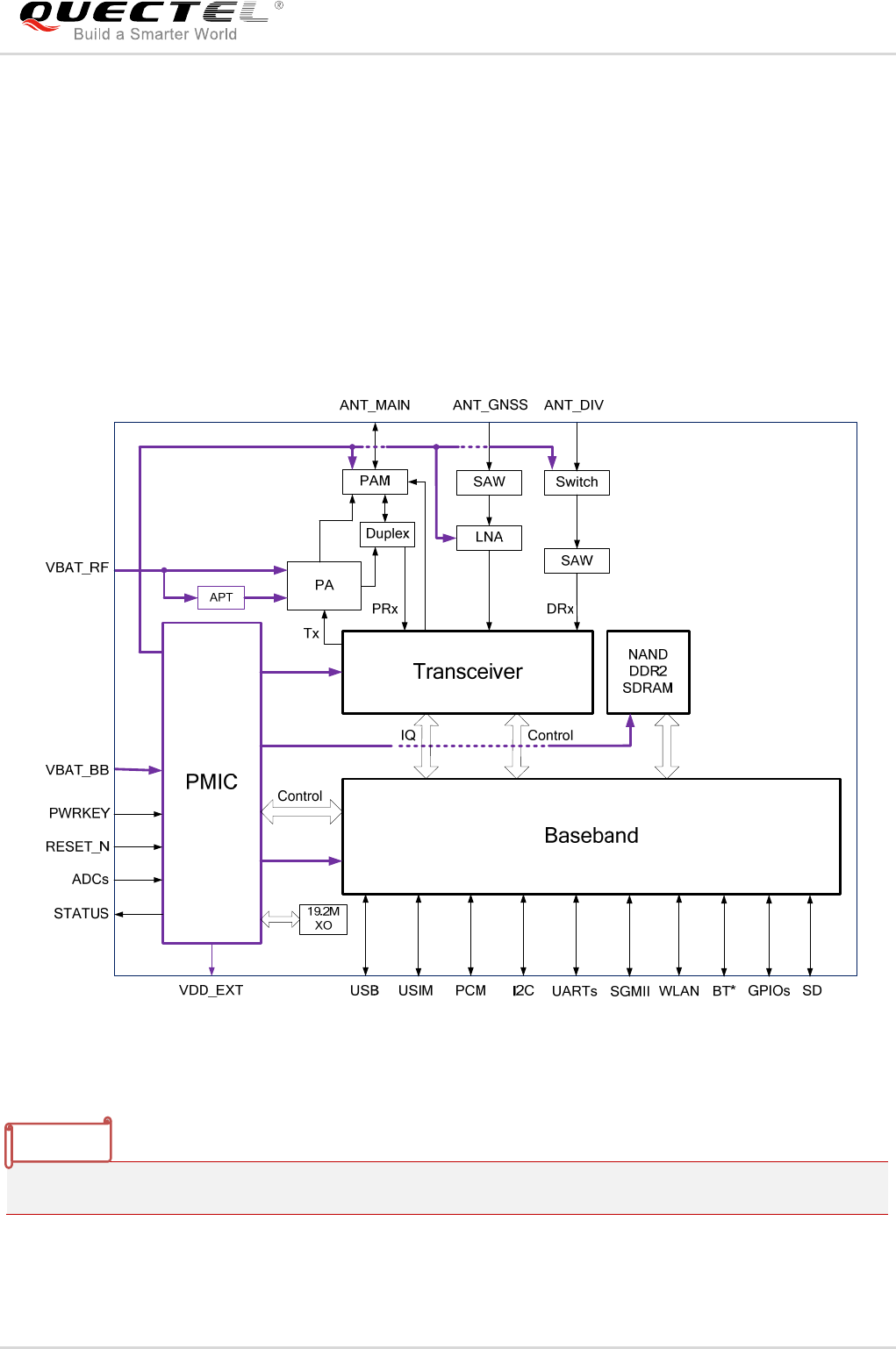
2.3. Functional Diagram
The following figure shows a block diagram of EC25 and illustrates the major functional parts.
Power management
Baseband
DDR+NAND flash
Radio frequency
Peripheral interfaces
Figure 1: Functional Diagram
“*” means under development.
NOTE

LTE Module Series
EC25 Hardware Design
EC25_Hardware_Design 21 / 112
2.4. Evaluation Board
In order to help customers develop applications with EC25, Quectel supplies an evaluation board (EVB),
USB to RS-232 converter cable, earphone, antenna and other peripherals to control or test the module.

LTE Module Series
EC25 Hardware Design
EC25_Hardware_Design 22 / 112
3 Application Interfaces
3.1. General Description
EC25 is equipped with 80 LCC pads plus 64 LGA pads that can be connected to cellular application
platform. Sub-interfaces included in these pads are described in detail in the following chapters:
Power supply
(U)SIM interface
USB interface
UART interfaces
PCM and I2C interfaces
SD card interface
ADC interfaces
Status indication
SGMII interface
Wireless connectivity interfaces
USB_BOOT interface
LTE Module Series
EC25 Hardware Design
EC25_Hardware_Design 23 / 112
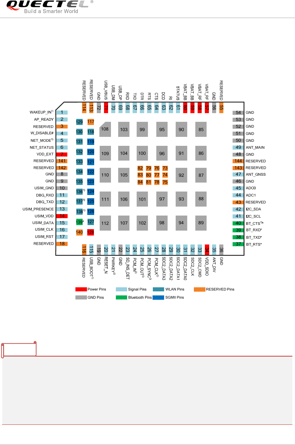
3.2. Pin Assignment
The following figure shows the pin assignment of EC25 module.
Figure 2: Pin Assignment (Top View)
1. 1) means that these pins cannot be pulled up before startup.
2. 2) PWRKEY output voltage is 0.8V because of the diode drop in the Qualcomm chipset.
3. 3) means these interface functions are only supported on Telematics version.
4. Pads 37~40, 118, 127 and 129~139 are used for wireless connectivity interfaces, among which pads
118, 127 and 129~138 are WLAN function pins, and the rest are Bluetooth (BT) function pins. BT
function is under development.
5. Pads 119~126 and 128 are used for SGMII interface.
NOTES

LTE Module Series
EC25 Hardware Design
EC25_Hardware_Design 24 / 112
6. Pads 24~27 are multiplexing pins used for audio design on the EC25 module and BT function on the
BT module.
7. Keep all RESERVED pins and unused pins unconnected.
8. GND pads 85~112 should be connected to ground in the design, and RESERVED pads 73~84
should not be designed in schematic and PCB decal, and these pins should be served as a keep out
area.
9. “*” means under development.
3.3. Pin Description
The following tables show the pin definition of EC25 modules.
Table 3: I/O Parameters Definition
Table 4: Pin Description
Type Description
IO Bidirectional
DI Digital input
DO Digital output
PI Power input
PO Power output
AI Analog input
AO Analog output
OD Open drain
Power Supply
Pin Name Pin No. I/O Description DC Characteristics Comment
VBAT_BB 59, 60 PI
Power supply for
module’s baseband
part
Vmax=4.3V
Vmin=3.3V
Vnorm=3.8V
It must be able to
provide sufficient
current up to 0.8A.
LTE Module Series
EC25 Hardware Design
EC25_Hardware_Design 25 / 112
VBAT_RF 57, 58 PI Power supply for
module’s RF part
Vmax=4.3V
Vmin=3.3V
Vnorm=3.8V
It must be able to
provide sufficient
current up to 1.8A in a
burst transmission.
VDD_EXT 7 PO
Provide 1.8V for
external circuit
Vnorm=1.8V
IOmax=50mA
Power supply for
external GPIO’s pull-up
circuits.
GND
8, 9, 19,
22, 36, 46,
48, 50~54,
56, 72,
85~112
Ground
Turn on/off
Pin Name Pin No. I/O Description DC Characteristics Comment
PWRKEY 21 DI
Turn on/off the
module
VIHmax=2.1V
VIHmin=1.3V
VILmax=0.5V
The output voltage is
0.8V because of the
diode drop in the
Qualcomm chipset.
RESET_N 20 DI Reset the module
VIHmax=2.1V
VIHmin=1.3V
VILmax=0.5V
If unused, keep it
open.
Status Indication
Pin Name Pin No. I/O Description DC Characteristics Comment
STATUS 61 OD
Indicate the module
operating status
The drive current
should be less than
0.9mA.
An external pull-up
resistor is required. If
unused, keep it open.
NET_MODE 5 DO
Indicate the module
network registration
mode
VOHmin=1.35V
VOLmax=0.45V
1.8V power domain.
Cannot be pulled up
before startup.
If unused, keep it
open.
NET_
STATUS 6 DO
Indicate the module
network activity
status
VOHmin=1.35V
VOLmax=0.45V
1.8V power domain.
If unused, keep it
open.
USB Interface
Pin Name Pin No. I/O Description DC Characteristics Comment
USB_VBUS 71 PI USB detection
Vmax=5.25V
Vmin=3.0V
Vnorm=5.0V
Typical: 5.0V
If unused, keep it
open.

LTE Module Series
EC25 Hardware Design
EC25_Hardware_Design 26 / 112
USB_DP 69 IO
USB differential data
bus (+)
Compliant with USB
2.0 standard
specification.
Require differential
impedance of 90Ω.
If unused, keep it
open.
USB_DM 70 IO
USB differential data
bus (-)
Compliant with USB
2.0 standard
specification.
Require differential
impedance of 90Ω.
If unused, keep it
open.
(U)SIM Interface
Pin Name Pin No. I/O Description DC Characteristics Comment
USIM_GND 10 Specified ground for
(U)SIM card
USIM_
PRESENCE 13 DI
(U)SIM card
insertion detection
VILmin=-0.3V
VILmax=0.6V
VIHmin=1.2V
VIHmax=2.0V
1.8V power domain.
If unused, keep it
open.
USIM_VDD 14 PO
Power supply for
(U)SIM card
For 1.8V(U)SIM:
Vmax=1.9V
Vmin=1.7V
For 3.0V(U)SIM:
Vmax=3.05V
Vmin=2.7V
IOmax=50mA
Either 1.8V or 3.0V is
supported by the
module automatically.
USIM_DATA 15 IO Data signal of
(U)SIM card
For 1.8V (U)SIM:
VILmax=0.6V
VIHmin=1.2V
VOLmax=0.45V
VOHmin=1.35V
For 3.0V (U)SIM:
VILmax=1.0V
VIHmin=1.95V
VOLmax=0.45V
VOHmin=2.55V
USIM_CLK 16 DO
Clock signal of
(U)SIM card
For 1.8V (U)SIM:
VOLmax=0.45V
VOHmin=1.35V
For 3.0V (U)SIM:
VOLmax=0.45V
VOHmin=2.55V
LTE Module Series
EC25 Hardware Design
EC25_Hardware_Design 27 / 112
USIM_RST 17 DO
Reset signal of
(U)SIM card
For 1.8V (U)SIM:
VOLmax=0.45V
VOHmin=1.35V
For 3.0V (U)SIM:
VOLmax=0.45V
VOHmin=2.55V
Main UART Interface
Pin Name Pin No. I/O Description DC Characteristics Comment
RI 62 DO Ring indicator VOLmax=0.45V
VOHmin=1.35V
1.8V power domain.
If unused, keep it
open.
DCD 63 DO
Data carrier
detection
VOLmax=0.45V
VOHmin=1.35V
1.8V power domain.
If unused, keep it
open.
CTS 64 DO Clear to send VOLmax=0.45V
VOHmin=1.35V
1.8V power domain.
If unused, keep it
open.
RTS 65 DI Request to send
VILmin=-0.3V
VILmax=0.6V
VIHmin=1.2V
VIHmax=2.0V
1.8V power domain.
If unused, keep it
open.
DTR 66 DI
Data terminal ready,
sleep mode control
VILmin=-0.3V
VILmax=0.6V
VIHmin=1.2V
VIHmax=2.0V
1.8V power domain.
Pulled up by default.
Low level wakes up
the module.
If unused, keep it
open.
TXD 67 DO Transmit data
VOLmax=0.45V
VOHmin=1.35V
1.8V power domain.
If unused, keep it
open.
RXD 68 DI Receive data
VILmin=-0.3V
VILmax=0.6V
VIHmin=1.2V
VIHmax=2.0V
1.8V power domain.
If unused, keep it
open.
Debug UART Interface
Pin Name Pin No. I/O Description DC Characteristics Comment
DBG_TXD 12 DO Transmit data VOLmax=0.45V
VOHmin=1.35V
1.8V power domain.
If unused, keep it
open.
DBG_RXD 11 DI Receive data VILmin=-0.3V 1.8V power domain.
LTE Module Series
EC25 Hardware Design
EC25_Hardware_Design 28 / 112
VILmax=0.6V
VIHmin=1.2V
VIHmax=2.0V
If unused, keep it
open.
ADC Interface
Pin Name Pin No. I/O Description DC Characteristics Comment
ADC0 45 AI
General purpose
analog to digital
converter
Voltage range:
0.3V to VBAT_BB
If unused, keep it
open.
ADC1 44 AI
General purpose
analog to digital
converter
Voltage range:
0.3V to VBAT_BB
If unused, keep it
open.
PCM Interface
Pin Name Pin No. I/O Description DC Characteristics Comment
PCM_IN 24 DI PCM data input
VILmin=-0.3V
VILmax=0.6V
VIHmin=1.2V
VIHmax=2.0V
1.8V power domain.
If unused, keep it
open.
PCM_OUT 25 DO PCM data output VOLmax=0.45V
VOHmin=1.35V
1.8V power domain.
If unused, keep it
open.
PCM_SYNC 26 IO
PCM data frame
synchronization
signal
VOLmax=0.45V
VOHmin=1.35V
VILmin=-0.3V
VILmax=0.6V
VIHmin=1.2V
VIHmax=2.0V
1.8V power domain.
In master mode, it is
an output signal. In
slave mode, it is an
input signal.
If unused, keep it
open.
PCM_CLK 27 IO PCM clock
VOLmax=0.45V
VOHmin=1.35V
VILmin=-0.3V
VILmax=0.6V
VIHmin=1.2V
VIHmax=2.0V
1.8V power domain.
In master mode, it is
an output signal. In
slave mode, it is an
input signal.
If unused, keep it
open.
I2C Interface
Pin Name Pin No. I/O Description DC Characteristics Comment
I2C_SCL 41 OD
I2C serial clock Used
for external codec.
External pull-up
resistor is required.
1.8V only. If unused,
keep it open.

LTE Module Series
EC25 Hardware Design
EC25_Hardware_Design 29 / 112
I2C_SDA 42 OD
I2C serial dataUsed
for external codec.
External pull-up
resistor is required.
1.8V only. If unused,
keep it open.
SD Card Interface
Pin Name Pin No. I/O Description DC Characteristics Comment
SDC2_
DATA3 28 IO
SD card SDIO bus
DATA3
1.8V signaling:
VOLmax=0.45V
VOHmin=1.4V
VILmin=-0.3V
VILmax=0.58V
VIHmin=1.27V
VIHmax=2.0V
3.0V signaling:
VOLmax=0.38V
VOHmin=2.01V
VILmin=-0.3V
VILmax=0.76V
VIHmin=1.72V
VIHmax=3.34V
SDIO signal level can
be selected according
to SD card supported
level, please refer to
SD 3.0 protocol for
more details.
If unused, keep it
open.
SDC2_
DATA2 29 IO
SD card SDIO bus
DATA2
1.8V signaling:
VOLmax=0.45V
VOHmin=1.4V
VILmin=-0.3V
VILmax=0.58V
VIHmin=1.27V
VIHmax=2.0V
3.0V signaling:
VOLmax=0.38V
VOHmin=2.01V
VILmin=-0.3V
VILmax=0.76V
VIHmin=1.72V
VIHmax=3.34V
SDIO signal level can
be selected according
to SD card supported
level, please refer to
SD 3.0 protocol for
more details.
If unused, keep it
open.
SDC2_
DATA1 30 IO
SD card SDIO bus
DATA1
1.8V signaling:
VOLmax=0.45V
VOHmin=1.4V
VILmin=-0.3V
VILmax=0.58V
VIHmin=1.27V
SDIO signal level can
be selected according
to SD card supported

LTE Module Series
EC25 Hardware Design
EC25_Hardware_Design 30 / 112
VIHmax=2.0V
3.0V signaling:
VOLmax=0.38V
VOHmin=2.01V
VILmin=-0.3V
VILmax=0.76V
VIHmin=1.72V
VIHmax=3.34V
level, please refer to
SD 3.0 protocol for
more details.
If unused, keep it
open.
SDC2_
DATA0 31 IO
SD card SDIO bus
DATA0
1.8V signaling:
VOLmax=0.45V
VOHmin=1.4V
VILmin=-0.3V
VILmax=0.58V
VIHmin=1.27V
VIHmax=2.0V
3.0V signaling:
VOLmax=0.38V
VOHmin=2.01V
VILmin=-0.3V
VILmax=0.76V
VIHmin=1.72V
VIHmax=3.34V
SDIO signal level can
be selected according
to SD card supported
level, please refer to
SD 3.0 protocol for
more details.
If unused, keep it
open.
SDC2_CLK 32 DO
SD card SDIO bus
clock
1.8V signaling:
VOLmax=0.45V
VOHmin=1.4V
3.0V signaling:
VOLmax=0.38V
VOHmin=2.01V
SDIO signal level can
be selected according
to SD card supported
level, please refer to
SD 3.0 protocol for
more details.
If unused, keep it
open.
SDC2_CMD 33 IO SD card SDIO bus
command
1.8V signaling:
VOLmax=0.45V
VOHmin=1.4V
VILmin=-0.3V
VILmax=0.58V
VIHmin=1.27V
VIHmax=2.0V
3.0V signaling:
VOLmax=0.38V
VOHmin=2.01V
VILmin=-0.3V
SDIO signal level can
be selected according
to SD card supported
level, please refer to
SD 3.0 protocol for
more details.
If unused, keep it
open.
LTE Module Series
EC25 Hardware Design
EC25_Hardware_Design 31 / 112
VILmax=0.76V
VIHmin=1.72V
VIHmax=3.34V
SD_INS_
DET 23 DI
SD card insertion
detect
VILmin=-0.3V
VILmax=0.6V
VIHmin=1.2V
VIHmax=2.0V
1.8V power domain.
If unused, keep it
open.
VDD_SDIO 34 PO
SD card SDIO bus
pull-up power IOmax=50mA
1.8V/2.85V
configurable. Cannot
be used for SD card
power. If unused,
keep it open.
SGMII Interface
Pin Name Pin No. I/O Description DC Characteristics Comment
EPHY_RST_
N 119 DO Ethernet PHY reset
For 1.8V:
VOLmax=0.45V
VOHmin=1.4V
For 2.85V:
VOLmax=0.35V
VOHmin=2.14V
1.8V/2.85V power
domain.
If unused, keep it
open.
EPHY_INT_N 120 DI Ethernet PHY
interrupt
VILmin=-0.3V
VILmax=0.6V
VIHmin=1.2V
VIHmax=2.0V
1.8V power domain.
If unused, keep it
open.
SGMII_
MDATA 121 IO
SGMII MDIO
(Management Data
Input/Output) data
For 1.8V:
VOLmax=0.45V
VOHmin=1.4V
VILmax=0.58V
VIHmin=1.27V
For 2.85V:
VOLmax=0.35V
VOHmin=2.14V
VILmax=0.71V
VIHmin=1.78V
1.8V/2.85V power
domain.
If unused, keep it
open.
SGMII_
MCLK 122 DO
SGMII MDIO
(Management Data
Input/Output) clock
For 1.8V:
VOLmax=0.45V
VOHmin=1.4V
For 2.85V:
VOLmax=0.35V
VOHmin=2.14V
1.8V/2.85V power
domain.
If unused, keep it
open.

LTE Module Series
EC25 Hardware Design
EC25_Hardware_Design 32 / 112
USIM2_VDD 128 PO SGMII MDIO pull-up
power source
Configurable power
source.
1.8V/2.85V power
domain.
External pull-up for
SGMII MDIO pins.
If unused, keep it
open.
SGMII_TX_M 123 AO SGMII transmission
- minus
Connect with a 0.1uF
capacitor, close to the
PHY side.
If unused, keep it
open.
SGMII_TX_P 124 AO SGMII transmission
- plus
Connect with a 0.1uF
capacitor, close to the
PHY side.
If unused, keep it
open.
SGMII_RX_P 125 AI SGMII receiving
- plus
Connect with a 0.1uF
capacitor, close to
EC25 module.
If unused, keep it
open.
SGMII_RX_M 126 AI SGMII receiving
-minus
Connect with a 0.1uF
capacitor, close to
EC25 module.
If unused, keep it
open.
Wireless Connectivity Interfaces
Pin Name Pin No. I/O Description DC Characteristics Comment
SDC1_
DATA3 129 IO
WLAN SDIO data
bus D3
VOLmax=0.45V
VOHmin=1.35V
VILmin=-0.3V
VILmax=0.6V
VIHmin=1.2V
VIHmax=2.0V
1.8V power domain.
If unused, keep it
open.
SDC1_
DATA2 130 IO
WLAN SDIO data
bus D2
VOLmax=0.45V
VOHmin=1.35V
VILmin=-0.3V
VILmax=0.6V
VIHmin=1.2V
VIHmax=2.0V
1.8V power domain.
If unused, keep it
open.

LTE Module Series
EC25 Hardware Design
EC25_Hardware_Design 33 / 112
SDC1_
DATA1 131 IO
WLAN SDIO data
bus D1
VOLmax=0.45V
VOHmin=1.35V
VILmin=-0.3V
VILmax=0.6V
VIHmin=1.2V
VIHmax=2.0V
1.8V power domain.
If unused, keep it
open.
SDC1_
DATA0 132 IO
WLAN SDIO data
bus D0
VOLmax=0.45V
VOHmin=1.35V
VILmin=-0.3V
VILmax=0.6V
VIHmin=1.2V
VIHmax=2.0V
1.8V power domain.
If unused, keep it
open.
SDC1_CLK 133 DO
WLAN SDIO bus
clock
VOLmax=0.45V
VOHmin=1.35V
1.8V power domain.
If unused, keep it
open.
SDC1_CMD 134 DO WLAN SDIO bus
command
VOLmax=0.45V
VOHmin=1.35V
1.8V power domain.
If unused, keep it
open.
PM_ENABLE 127 DO External power
control
VOLmax=0.45V
VOHmin=1.35V
1.8V power domain.
If unused, keep it
open.
WAKE_ON_
WIRELESS 135 DI
Wake up the host
(EC25 module) by
FC20 module
VILmin=-0.3V
VILmax=0.6V
VIHmin=1.2V
VIHmax=2.0V
1.8V power domain.
Active low.
If unused, keep it
open.
WLAN_EN 136 DO
WLAN function
control via FC20
module
VOLmax=0.45V
VOHmin=1.35V
1.8V power domain.
Active high.
Cannot be pulled up
before startup.
If unused, keep it
open.
COEX_UART
_RX 137 DI
LTE/WLAN&BT
coexistence signal
VILmin=-0.3V
VILmax=0.6V
VIHmin=1.2V
VIHmax=2.0V
1.8V power domain.
Cannot be pulled up
before startup.
If unused, keep it
open.
COEX_UART
_TX 138 DO
LTE/WLAN&BT
coexistence signal
VOLmax=0.45V
VOHmin=1.35V
1.8V power domain.
Cannot be pulled up
before startup.
If unused, keep it
open.
WLAN_SLP_
CLK 118 DO WLAN sleep clock If unused, keep it
open.
LTE Module Series
EC25 Hardware Design
EC25_Hardware_Design 34 / 112
BT_RTS* 37 DI
BT UART request to
send
VILmin=-0.3V
VILmax=0.6V
VIHmin=1.2V
VIHmax=2.0V
1.8V power domain.
If unused, keep it
open.
BT_TXD* 38 DO
BT UART transmit
data
VOLmax=0.45V
VOHmin=1.35V
1.8V power domain.
If unused, keep it
open.
BT_RXD* 39 DI
BT UART receive
data
VILmin=-0.3V
VILmax=0.6V
VIHmin=1.2V
VIHmax=2.0V
1.8V power domain.
If unused, keep it
open.
BT_CTS* 40 DO
BT UART clear to
send
VOLmax=0.45V
VOHmin=1.35V
1.8V power domain.
Cannot be pulled up
before startup.
If unused, keep it
open.
BT_EN* 139 DO
BT function control
via the BT module
VOLmax=0.45V
VOHmin=1.35V
1.8V power domain.
If unused, keep it
open.
RF Interface
Pin Name Pin No. I/O Description DC Characteristics Comment
ANT_DIV 35 AI
Diversity antenna
pad
50Ω impedance
If unused, keep it
open.
ANT_MAIN 49 IO Main antenna pad 50Ω impedance
ANT_GNSS 47 AI GNSS antenna pad
50Ω impedance
If unused, keep it
open.
GPIO Pins
Pin Name Pin No. I/O Description DC Characteristics Comment
WAKEUP_IN 1 DI Sleep mode control
VILmin=-0.3V
VILmax=0.6V
VIHmin=1.2V
VIHmax=2.0V
1.8V power domain.
Cannot be pulled up
before startup.
Low level wakes up
the module.
If unused, keep it
open.
W_DISABLE# 4 DI Airplane mode
control
VILmin=-0.3V
VILmax=0.6V
VIHmin=1.2V
1.8V power domain.
Pull-up by default.
At low voltage level,
LTE Module Series
EC25 Hardware Design
EC25_Hardware_Design 35 / 112
1. “*” means under development.
2. Pads 24~27 are multiplexing pins used for audio design on the EC25 module and BT function on the
BT module.
VIHmax=2.0V module can enter into
airplane mode.
If unused, keep it
open.
AP_READY 2 DI
Application
processor sleep
state detection
VILmin=-0.3V
VILmax=0.6V
VIHmin=1.2V
VIHmax=2.0V
1.8V power domain.
If unused, keep it
open.
USB_BOOT Interface
Pin Name Pin No. I/O Description DC Characteristics Comment
USB_BOOT 115 DI
Force the module to
enter into
emergency
download mode
VILmin=-0.3V
VILmax=0.6V
VIHmin=1.2V
VIHmax=2.0V
1.8V power domain.
Cannot be pulled up
before startup.
It is recommended to
reserve test point.
RESERVED Pins
Pin Name Pin No. I/O Description DC Characteristics Comment
RESERVED
3, 18, 43,
55, 73~84,
113, 114,
116, 117,
140-144.
Reserved Keep these pins
unconnected.
NOTES

LTE Module Series
EC25 Hardware Design
EC25_Hardware_Design 36 / 112
3.4. Operating Modes
The table below briefly summarizes the various operating modes referred in the following chapters.
Table 5: Overview of Operating Modes
3.5. Power Saving
3.5.1. Sleep Mode
EC25 is able to reduce its current consumption to a minimum value during the sleep mode. The following
section describes power saving procedures of EC25 module.
3.5.1.1. UART Application
If the host communicates with module via UART interface, the following preconditions can let the module
enter into sleep mode.
Execute AT+QSCLK=1 command to enable sleep mode.
Drive DTR to high level.
Mode Details
Normal
Operation
Idle Software is active. The module has registered on the network, and it is
ready to send and receive data.
Talk/Data Network connection is ongoing. In this mode, the power consumption is
decided by network setting and data transfer rate.
Minimum
Functionality
Mode
AT+CFUN command can set the module to a minimum functionality mode without
removing the power supply. In this case, both RF function and (U)SIM card will be
invalid.
Airplane Mode AT+CFUN command or W_DISABLE# pin can set the module to airplane mode. In
this case, RF function will be invalid.
Sleep Mode
In this mode, the current consumption of the module will be reduced to the minimal
level. During this mode, the module can still receive paging message, SMS, voice
call and TCP/UDP data from the network normally.
Power Down
Mode
In this mode, the power management unit shuts down the power supply. Software is
not active. The serial interface is not accessible. Operating voltage (connected to
VBAT_RF and VBAT_BB) remains applied.
LTE Module Series
EC25 Hardware Design
EC25_Hardware_Design 37 / 112
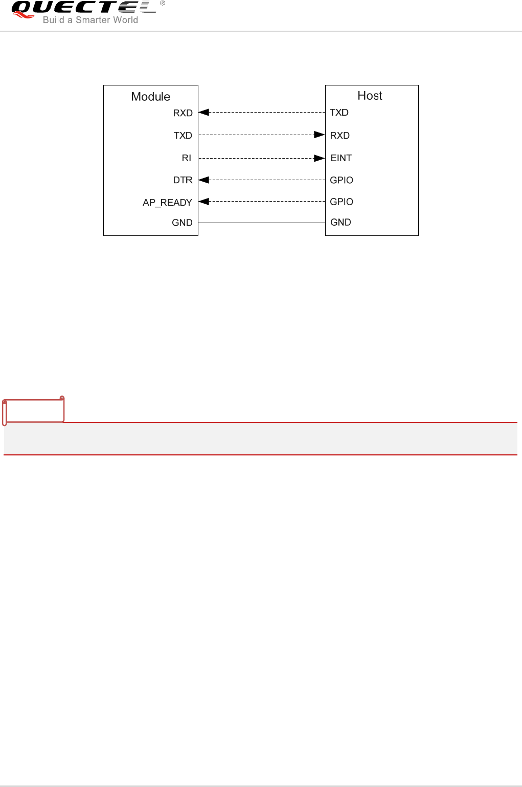
The following figure shows the connection between the module and the host.
Figure 3: Sleep Mode Application via UART
Driving the host DTR to low level will wake up the module.
When EC25 has a URC to report, RI signal will wake up the host. Please refer to Chapter 3.17 for
details about RI behaviors.
AP_READY will detect the sleep state of the host (can be configured to high level or low level
detection). Please refer to AT+QCFG="apready"* command for details.
“*” means under development.
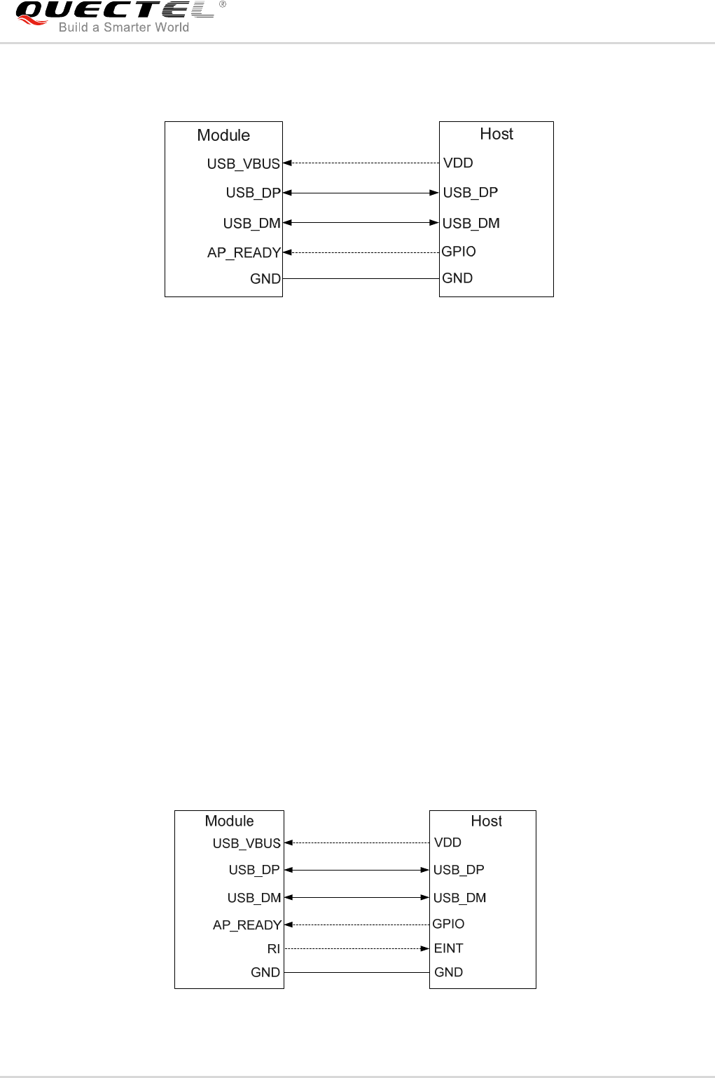
3.5.1.2. USB Application with USB Remote Wakeup Function
If the host supports USB suspend/resume and remote wakeup function, the following three preconditions
must be met to let the module enter into the sleep mode.
Execute AT+QSCLK=1 command to enable sleep mode.
Ensure the DTR is held at high level or keep it open.
The host’s USB bus, which is connected with the module’s USB interface, enters into suspended
state.
NOTE
LTE Module Series
EC25 Hardware Design
EC25_Hardware_Design 38 / 112
The following figure shows the connection between the module and the host.
Figure 4: Sleep Mode Application with USB Remote Wakeup
Sending data to EC25 through USB will wake up the module.
When EC25 has a URC to report, the module will send remote wake-up signals via USB bus so as to
wake up the host.
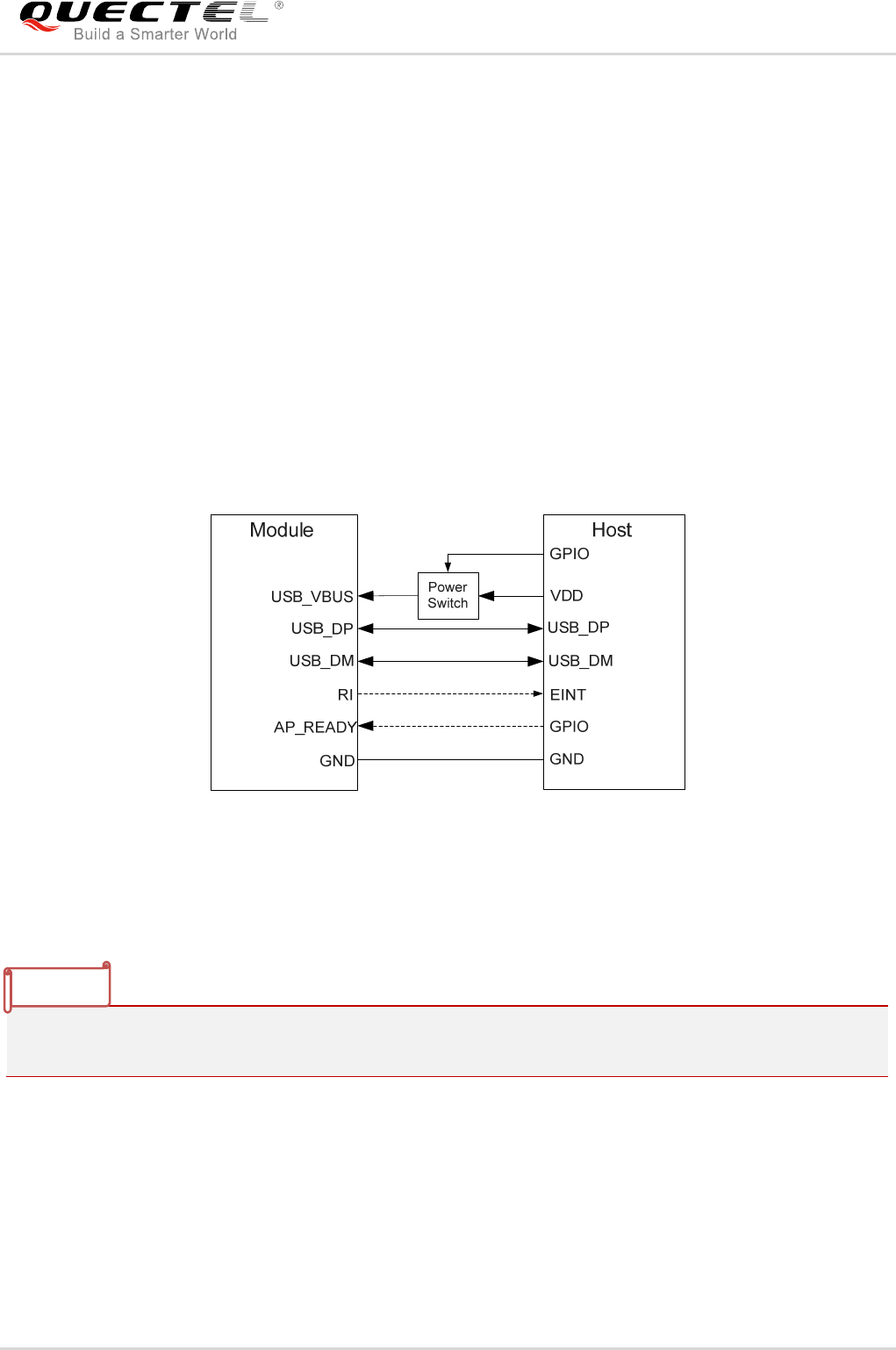
3.5.1.3. USB Application with USB Suspend/Resume and RI Function
If the host supports USB suspend/resume, but does not support remote wake-up function, the RI signal is
needed to wake up the host.
There are three preconditions to let the module enter into the sleep mode.
Execute AT+QSCLK=1 command to enable the sleep mode.
Ensure the DTR is held at high level or keep it open.
The host’s USB bus, which is connected with the module’s USB interface, enters into suspended
state.
The following figure shows the connection between the module and the host.
Figure 5: Sleep Mode Application with RI
LTE Module Series
EC25 Hardware Design
EC25_Hardware_Design 39 / 112
Sending data to EC25 through USB will wake up the module.
When EC25 has a URC to report, RI signal will wake up the host.
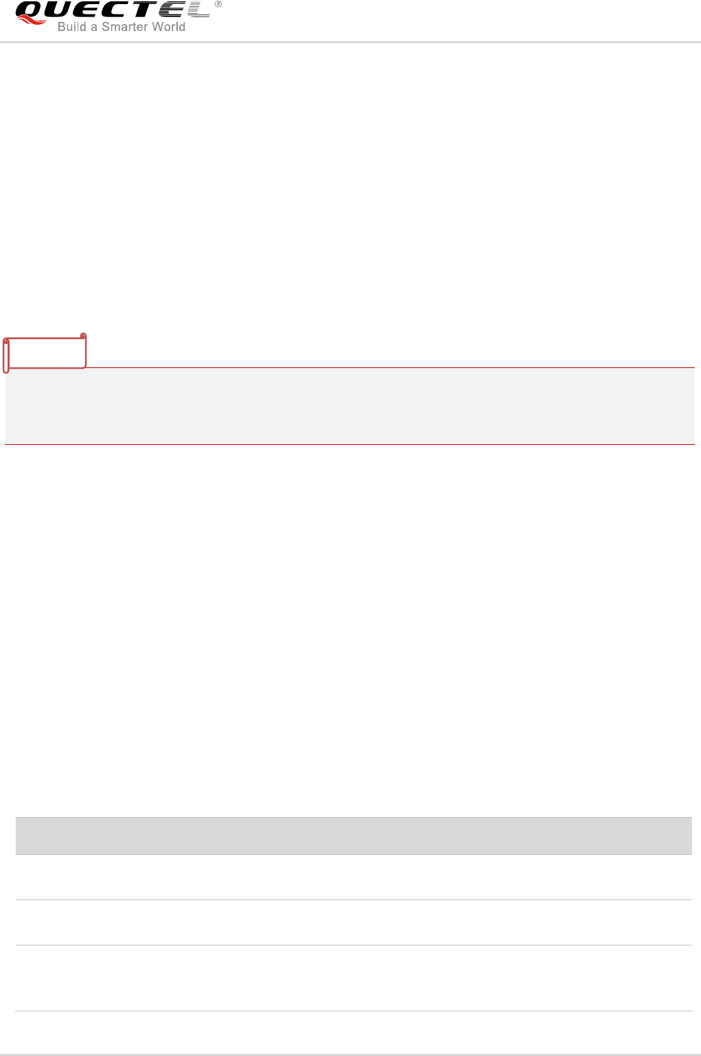
3.5.1.4. USB Application without USB Suspend Function
If the host does not support USB suspend function, USB_VBUS should be disconnected via an additional
control circuit to let the module enter into sleep mode.
Execute AT+QSCLK=1 command to enable sleep mode.
Ensure the DTR is held at high level or keep it open.
Disconnect USB_VBUS.
The following figure shows the connection between the module and the host.
Figure 6: Sleep Mode Application without Suspend Function
Switching on the power switch to supply power to USB_VBUS will wake up the module.
Please pay attention to the level match shown in dotted line between the module and the host. For more
details about EC25 power management application, please refer to document [1].
3.5.2. Airplane Mode
When the module enters into airplane mode, the RF function does not work, and all AT commands
correlative with RF function will be inaccessible. This mode can be set via the following ways.
NOTE
LTE Module Series
EC25 Hardware Design
EC25_Hardware_Design 40 / 112
Hardware:
The W_DISABLE# pin is pulled up by default; driving it to low level will let the module enter into airplane
mode.
Software:
AT+CFUN command provides the choice of the functionality level through setting <fun> into 0, 1 or 4.
AT+CFUN=0: Minimum functionality mode. Both (U)SIM and RF functions are disabled.
AT+CFUN=1: Full functionality mode (by default).
AT+CFUN=4: Airplane mode. RF function is disabled.
1. The W_DISABLE# control function is disabled in firmware by default. It can be enabled by
AT+QCFG="airplanecontrol" command, and this command is under development.
2. The execution of AT+CFUN command will not affect GNSS function.
3.6. Power Supply
3.6.1. Power Supply Pins
EC25 provides four VBAT pins to connect with the external power supply, and there are two separate
voltage domains for VBAT.
Two VBAT_RF pins for module’s RF part
Two VBAT_BB pins for module’s baseband part
The following table shows the details of VBAT pins and ground pins.
Table 6: VBAT and GND Pins
Pin Name Pin No. Description Min. Typ. Max. Unit
VBAT_RF 57, 58 Power supply for module’s RF
part 3.3 3.8 4.3 V
VBAT_BB 59, 60 Power supply for module’s
baseband part 3.3 3.8 4.3 V
GND
8, 9, 19, 22, 36,
46, 48, 50~54,
56, 72, 85~112
Ground - 0 - V
NOTES
LTE Module Series
EC25 Hardware Design
EC25_Hardware_Design 41 / 112
3.6.2. Decrease Voltage Drop
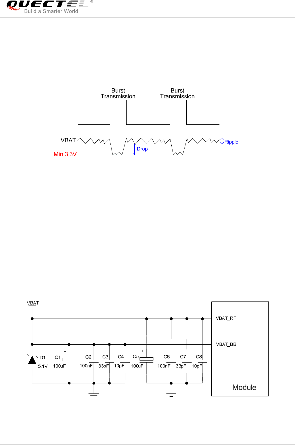
The power supply range of the module is from 3.3V to 4.3V. Please make sure that the input voltage will
never drop below 3.3V. The following figure shows the voltage drop during burst transmission in 2G
network. The voltage drop will be less in 3G and 4G networks.
Figure 7: Power Supply Limits during Burst Transmission
To decrease voltage drop, a bypass capacitor of about 100µF with low ESR (ESR=0.7Ω) should be used,
and a multi-layer ceramic chip (MLCC) capacitor array should also be reserved due to its ultra-low ESR. It
is recommended to use three ceramic capacitors (100nF, 33pF, 10pF) for composing the MLCC array,
and place these capacitors close to VBAT_BB/VBAT_RF pins. The main power supply from an external
application has to be a single voltage source and can be expanded to two sub paths with star structure.
The width of VBAT_BB trace should be no less than 1mm; and the width of VBAT_RF trace should be no
less than 2mm. In principle, the longer the VBAT trace is, the wider it will be.
In addition, in order to get a stable power source, it is suggested that a zener diode whose reverse zener
voltage is 5.1V and dissipation power is more than 0.5W should be used. The following figure shows the
star structure of the power supply.
Figure 8: Star Structure of the Power Supply
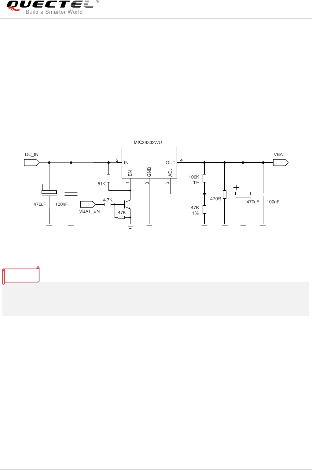
LTE Module Series
EC25 Hardware Design
EC25_Hardware_Design 42 / 112
3.6.3. Reference Design for Power Supply
Power design for the module is very important, as the performance of the module largely depends on the
power source. The power supply should be able to provide sufficient current up to 2A at least. If the
voltage drop between the input and output is not too high, it is suggested that an LDO should be used to
supply power for the module. If there is a big voltage difference between the input source and the desired
output (VBAT), a buck converter is preferred to be used as the power supply.
The following figure shows a reference design for +5V input power source. The typical output of the power
supplyis about 3.8V and the maximum load current is 3A.
Figure 9: Reference Circuit of Power Supply
In order to avoid damaging internal flash, please do not switch off the power supply when the module
works normally. Only after the module is shutdown by PWRKEY or AT command, then the power supply
can be cut off.
3.6.4. Monitor the Power Supply
AT+CBC command can be used to monitor the VBAT_BB voltage value. For more details, please refer to
document [2].
3.7. Turn on and off Scenarios
3.7.1. Turn on Module Using the PWRKEY
The following table shows the pin definition of PWRKEY.
NOTE
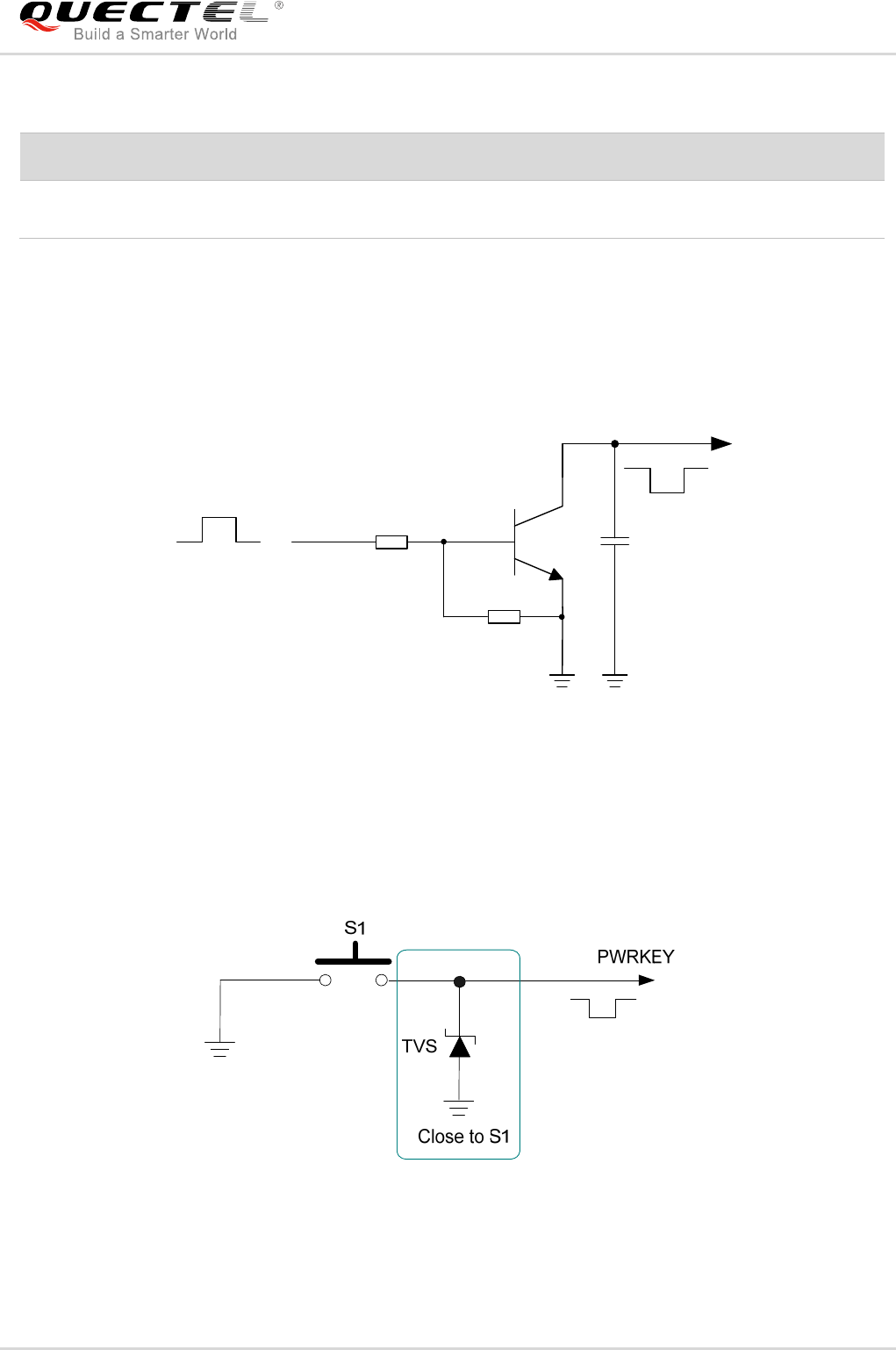
LTE Module Series
EC25 Hardware Design
EC25_Hardware_Design 43 / 112
Table 7: Pin Definition of PWRKEY
When EC25 is in power down mode, it can be turned on to normal mode by driving the PWRKEY pin to a
low level for at least 500ms. It is recommended to use an open drain/collector driver to control the
PWRKEY. After STATUS pin (require external pull-up) outputting a low level, PWRKEY pin can be
released. A simple reference circuit is illustrated in the following figure.
Turn on pulse
PWRKEY
4.7K
47K
≥ 500ms
10nF
Figure 10: Turn on the Module by Using Driving Circuit
The other way to control the PWRKEY is using a button directly. When pressing the key, electrostatic
strike may generate from finger. Therefore, a TVS component is indispensable to be placed nearby the
button for ESD protection. A reference circuit is shown in the following figure.
Figure 11: Turn on the Module by Using Button
Pin Name Pin No. I/O Description Comment
PWRKEY 21 DI Turn on/off the module The output voltage is 0.8V because of
the diode drop in the Qualcomm chipset.
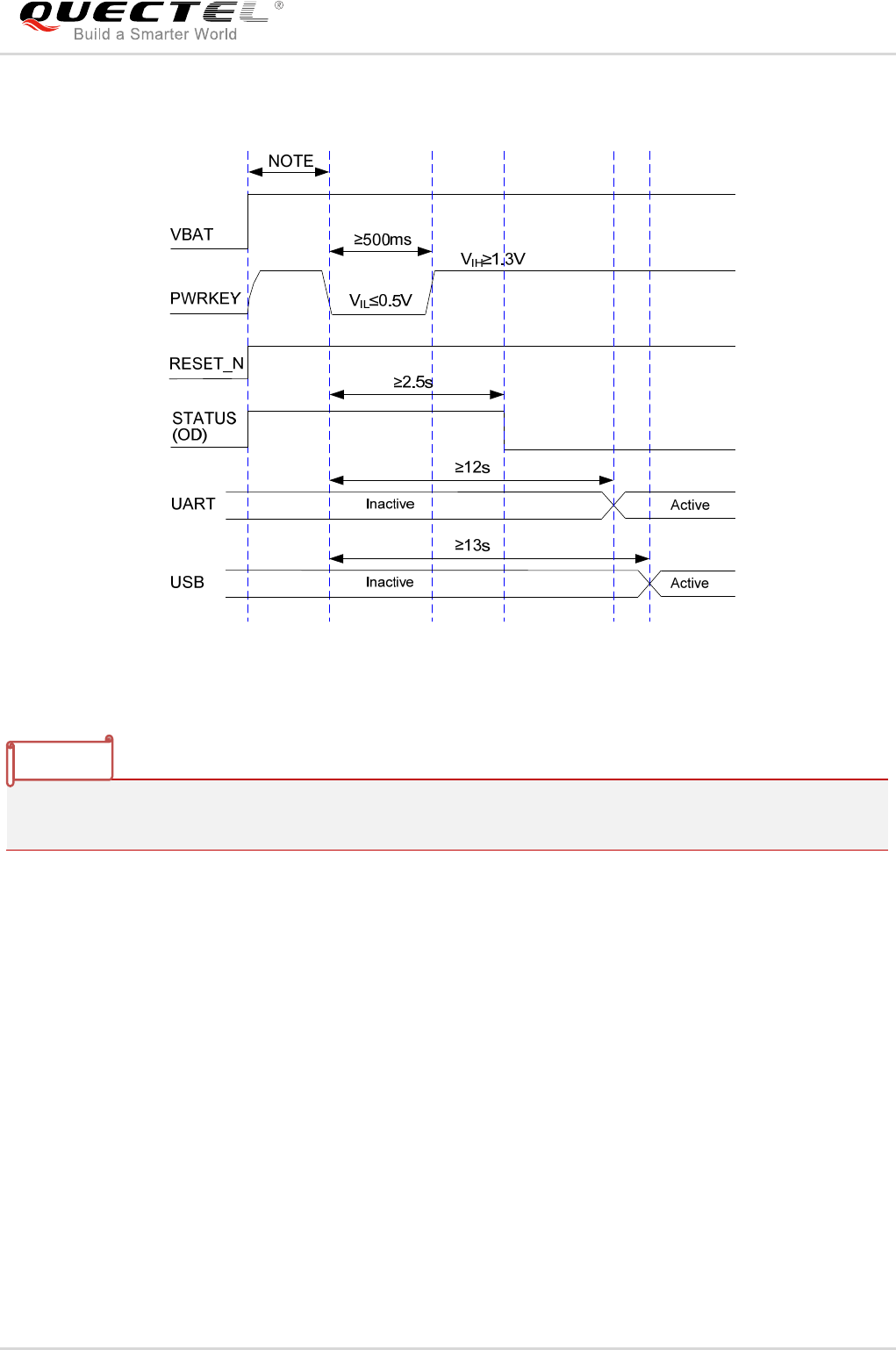
LTE Module Series
EC25 Hardware Design
EC25_Hardware_Design 44 / 112
The turn on scenario is illustrated in the following figure.
Figure 12: Timing of Turning on Module
Please make sure that VBAT is stable before pulling down PWRKEY pin. The time between them should
be no no less than 30ms.
3.7.2. Turn off Module
The following procedures can be used to turn off the module:
Normal power down procedure: Turn off the module using the PWRKEY pin.
Normal power down procedure: Turn off the module using AT+QPOWD command.
3.7.2.1. Turn off Module Using the PWRKEY Pin
Driving the PWRKEY pin to a low level voltage for at least 650ms, the module will execute power-down
procedure after the PWRKEY is released. The power-down scenario is illustrated in the following figure.
NOTE
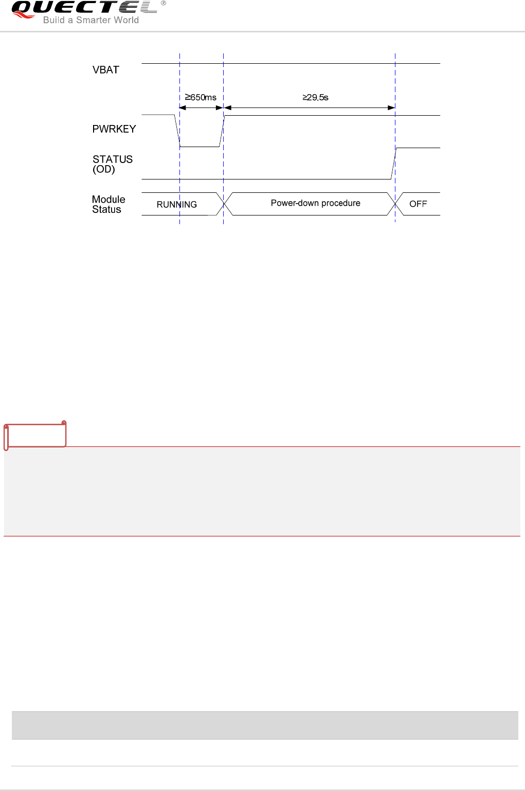
LTE Module Series
EC25 Hardware Design
EC25_Hardware_Design 45 / 112
Figure 13: Timing of Turning off Module
3.7.2.2. Turn off Module Using AT Command
It is also a safe way to use AT+QPOWD command to turn off the module, which is similar to turning off the
module via PWRKEY pin.
Please refer to document [2] for details about AT+QPOWD command.
1. Inorder to avoid damaging internal flash, please do not switch off the power supply when the module
works normally. Only after the module is shut down by PWRKEY or AT command, then the power
supply can be cut off.
2. When turn off module with AT command, please keep PWRKEY at high level after the execution of
power-off command. Otherwise the module will be turned on again after successfully turn-off.
3.8. Reset the Module
The RESET_N pin can be used to reset the module. The module can be reset by driving RESET_N to a
low level voltage for time between 150ms and 460ms.
Table 8: RESET_N Pin Description
Pin Name Pin No. I/O Description Comment
RESET_N 20 DI Reset the module 1.8V power domain
NOTES
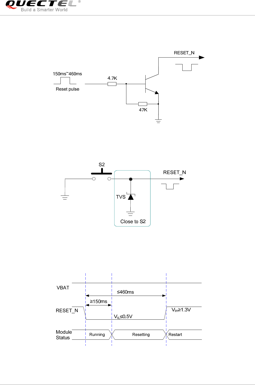
LTE Module Series
EC25 Hardware Design
EC25_Hardware_Design 46 / 112
The recommended circuit is similar to the PWRKEY control circuit. An open drain/collector driver or button
can be used to control the RESET_N.
Figure 14: Reference Circuit of RESET_N by Using Driving Circuit
Figure 15: Reference Circuit of RESET_N by Using Button
The reset scenario is illustrated inthe following figure.
Figure 16: Timing of Resetting Module
LTE Module Series
EC25 Hardware Design
EC25_Hardware_Design 47 / 112
1. Use RESET_N only when turning off the module by AT+QPOWD command and PWRKEY pin failed.
2. Ensure that there is no large capacitance on PWRKEY and RESET_N pins.
3.9. (U)SIM Interface
The(U)SIM interface circuitry meets ETSI and IMT-2000 requirements. Both 1.8V and 3.0V (U)SIM cards
are supported.
Table 9: Pin Definition of the (U)SIM Interface
EC25 supports (U)SIM card hot-plug via the USIM_PRESENCE pin. The function supports low level and
high level detections, and it is disabled by default. Please refer to document [2] for more details about
AT+QSIMDET command.
Pin Name Pin No. I/O Description Comment
USIM_VDD 14 PO Power supply for (U)SIM card Either 1.8V or 3.0V is supported
by the module automatically.
USIM_DATA 15 IO Data signal of (U)SIM card
USIM_CLK 16 DO Clock signal of (U)SIM card
USIM_RST 17 DO Reset signal of (U)SIM card
USIM_
PRESENCE 13 DI (U)SIM card insertion detection
USIM_GND 10 Specified ground for (U)SIM card
NOTES
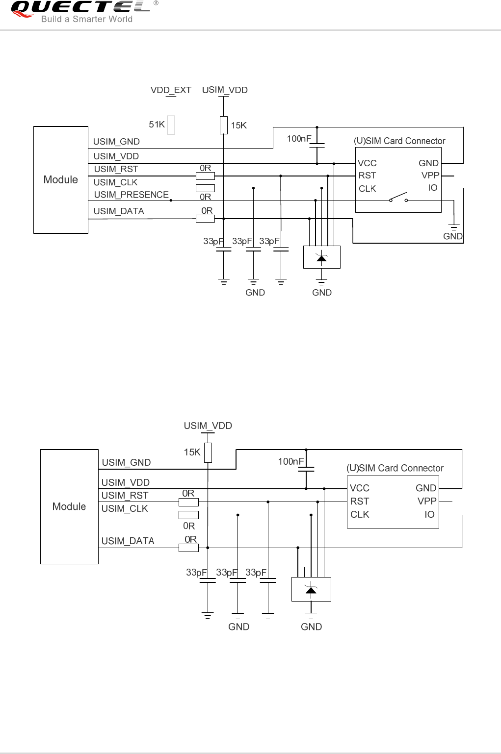
LTE Module Series
EC25 Hardware Design
EC25_Hardware_Design 48 / 112
The following figure shows a reference design for (U)SIM interface with an 8-pin (U)SIM card connector.
Figure 17: Reference Circuit of (U)SIM Interface with an 8-Pin (U)SIM Card Connector
If (U)SIM card detection function is not needed, please keep USIM_PRESENCE unconnected. A
reference circuit for (U)SIM interface with a 6-pin (U)SIM card connector is illustrated in the following
figure.
Figure 18: Reference Circuit of (U)SIM Interface with a 6-Pin (U)SIM Card Connector
In order to enhance the reliability and availability of the (U)SIM card in customers’ applications, please
follow the criteria below in (U)SIM circuit design:

LTE Module Series
EC25 Hardware Design
EC25_Hardware_Design 49 / 112
Keep placement of (U)SIM card connector to the module as close as possible. Keep the trace length
as less than 200mm as possible.
Keep (U)SIM card signals away from RF and VBAT traces.
Assure the ground between the module and the (U)SIM card connector short and wide. Keep the
trace width of ground and USIM_VDD no less than 0.5mm to maintain the same electric potential.
Make sure the bypass capacitor between USIM_VDD and USIM_GND less than 1uF, and place it as
close to (U)SIM card connector as possible. If the ground is complete on customers’ PCB,
USIM_GND can be connected to PCB ground directly.
To avoid cross-talk between USIM_DATA and USIM_CLK, keep them away from each other and
shield them with surrounded ground.
In order to offer good ESD protection, it is recommended to add a TVS diode array whose parasitic
capacitance should not be more than 15pF. The 0Ω resistors should be added in series between the
module and the (U)SIM card to facilitate debugging. The 33pF capacitors are used for filtering
interference of EGSM900. Please note that the (U)SIM peripheral circuit should be close to the
(U)SIM card connector.
The pull-up resistor on USIM_DATA line can improve anti-jamming capability when long layout trace
and sensitive occasion are applied, and it should be placed close to the (U)SIM card connector.
3.10. USB Interface
EC25 contains one integrated Universal Serial Bus (USB) interface which complies with the USB 2.0
specification and supports high-speed (480Mbps) and full-speed (12Mbps) modes. The USB interface is
used for AT command communication, data transmission, GNSS NMEA sentences output, software
debugging, firmware upgrade and voice over USB*. The following table shows the pin definition of USB
interface.
Table 10: Pin Description of USB Interface
For more details about the USB 2.0 specifications, please visit http://www.usb.org/home.
Pin Name Pin No. I/O Description Comment
USB_DP 69 IO USB differential data bus (+) Require differential
impedance of 90Ω
USB_DM 70 IO USB differential data bus (-) Require differential
impedance of 90Ω
USB_VBUS 71 PI USB connection detection Typical 5.0V
GND 72 Ground
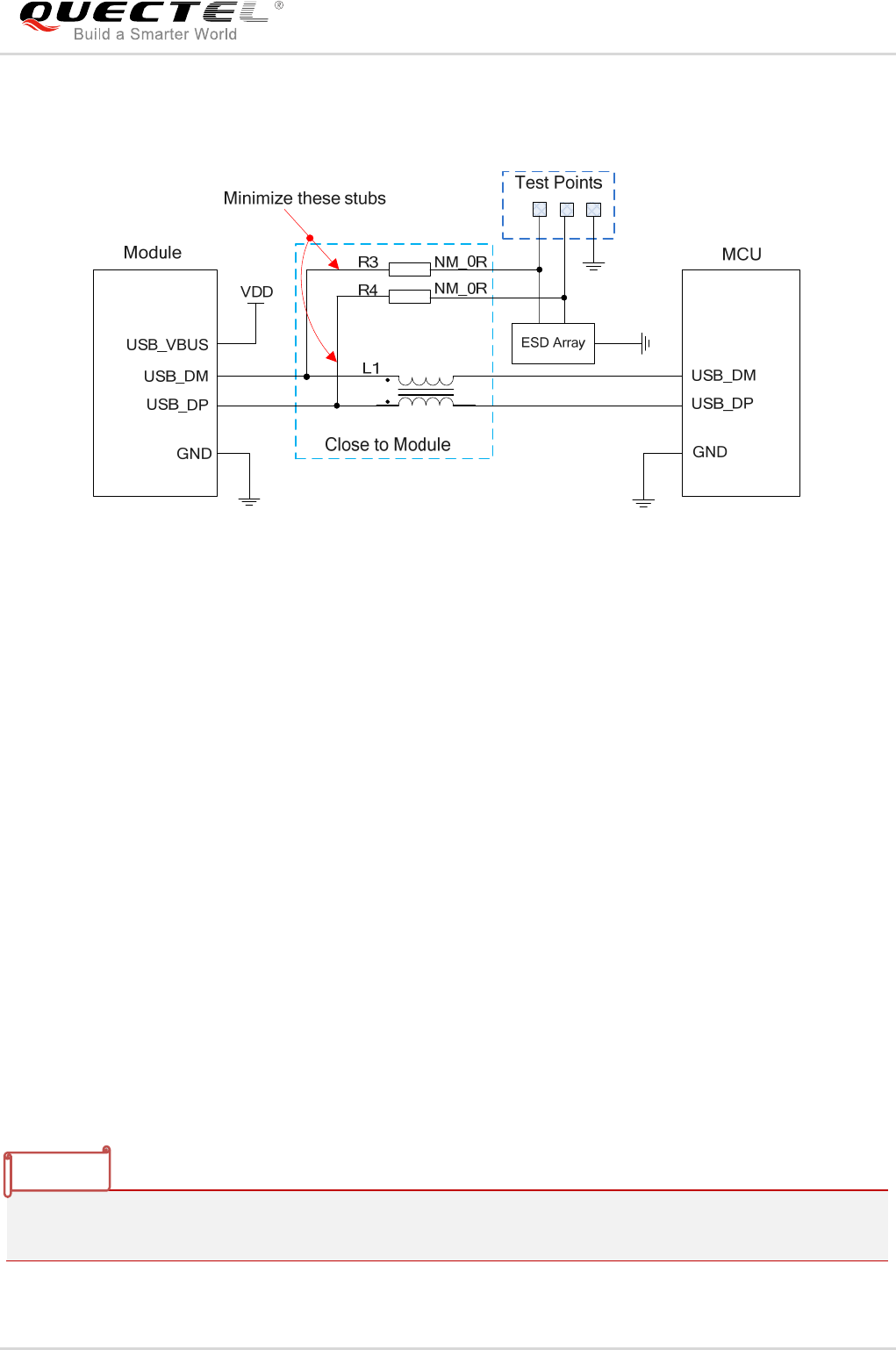
LTE Module Series
EC25 Hardware Design
EC25_Hardware_Design 50 / 112
The USB interface is recommended to be reserved for firmware upgrade in customers’ designs. The
following figure shows a reference circuit of USB interface.
Figure 19: Reference Circuit of USB Application
A common mode choke L1 is recommended to be added in series between the module and customer’s
MCU in order to suppress EMI spurious transmission. Meanwhile, the 0Ω resistors (R3 and R4) should be
added in series between the module and the test points so as to facilitate debugging, and the resistors are
not mounted by default. In order to ensure the integrity of USB data line signal, L1/R3/R4 components
must be placed close to the module, and also these resistors should be placed close to each other. The
extra stubs of trace must be as short as possible.
The following principles should be complied with when design the USB interface, so as to meet USB 2.0
specification.
It is important to route the USB signal traces as differential pairs with total grounding. The impedance
of USB differential trace is 90Ω.
Do not route signal traces under crystals, oscillators, magnetic devices and RF signal traces. It is
important to route the USB differential traces in inner-layer with ground shielding on not only upper
and lower layers but also right and left sides.
Pay attention to the influence of junction capacitance of ESD protection components on USB data
lines. Typically, the capacitance value should be less than 2pF.
Keep the ESD protection components to the USB connector as close as possible.
1. EC25 module can only be used as a slave device.
2. “*” means under development.
NOTES
LTE Module Series
EC25 Hardware Design
EC25_Hardware_Design 51 / 112
3.11. UART Interfaces
The module provides two UART interfaces: the main UART interface and the debug UART interface. The
following shows their features.
The main UART interface supports 4800bps, 9600bps, 19200bps, 38400bps, 57600bps, 115200bps,
230400bps, 460800bps and 921600bps baud rates, and the default is 115200bps. This interface is
used for data transmission and AT command communication.
The debug UART interface supports 115200bps baud rate. It is used for Linux console and log
output.
The following tables show the pin definition of the UART interfaces.
Table 11: Pin Definition of Main UART Interface
Table 12: Pin Definition of Debug UART Interface
Pin Name Pin No. I/O Description Comment
RI 62 DO Ring indicator
1.8V power domain
DCD 63 DO Data carrier detection
CTS 64 DO Clear to send
RTS 65 DI Request to send
DTR 66 DI Data terminal ready
TXD 67 DO Transmit data
RXD 68 DI Receive data
Pin Name Pin No. I/O Description Comment
DBG_TXD 12 DO Transmit data
1.8V power domain
DBG_RXD 11 DI Receive data
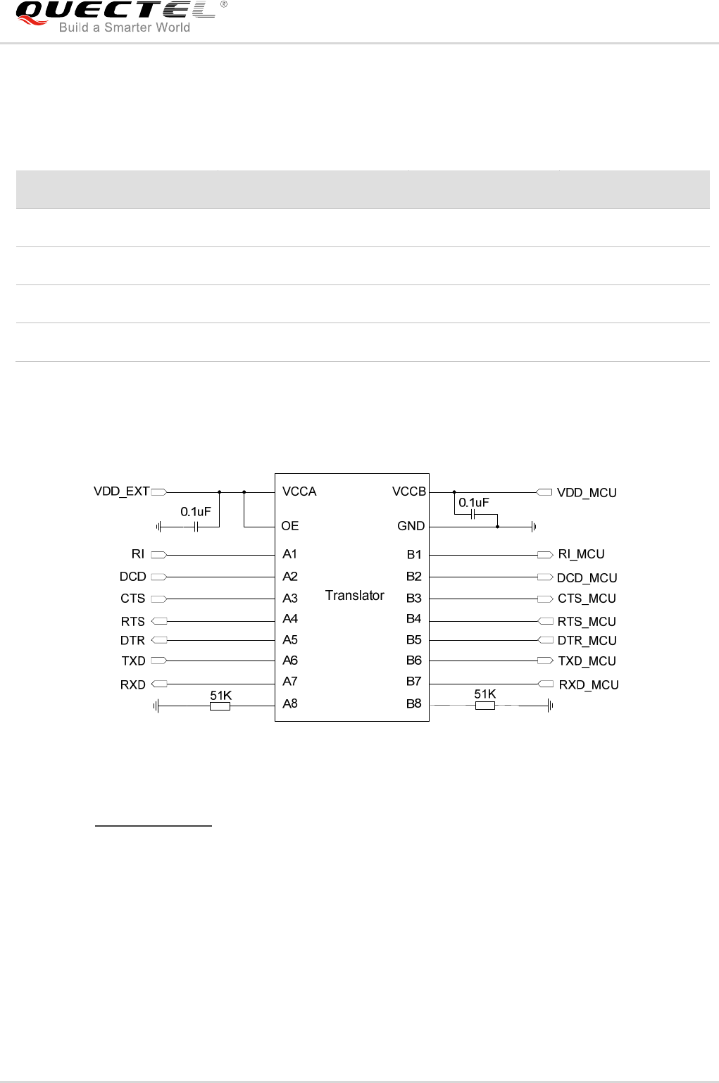
LTE Module Series
EC25 Hardware Design
EC25_Hardware_Design 52 / 112
The logic levels are described in the following table.
Table 13: Logic Levels of Digital I/O
The module provides 1.8V UART interface. A level translator should be used if customers’ application is
equipped with a 3.3V UART interface. A level translator TXS0108EPWR provided by Texas Instruments
is recommended. The following figure shows a reference design.
Figure 20: Reference Circuit with Translator Chip
Please visit http://www.ti.com for more information.
Another example with transistor translation circuit is shown as below. The circuit design of dotted line
section can refer to the design of solid line section, in terms of both module’s input and output circuit
designs, but please pay attention to the direction of connection.
Parameter Min. Max. Unit
VIL -0.3 0.6 V
VIH 1.2 2.0 V
VOL 0 0.45 V
VOH 1.35 1.8 V
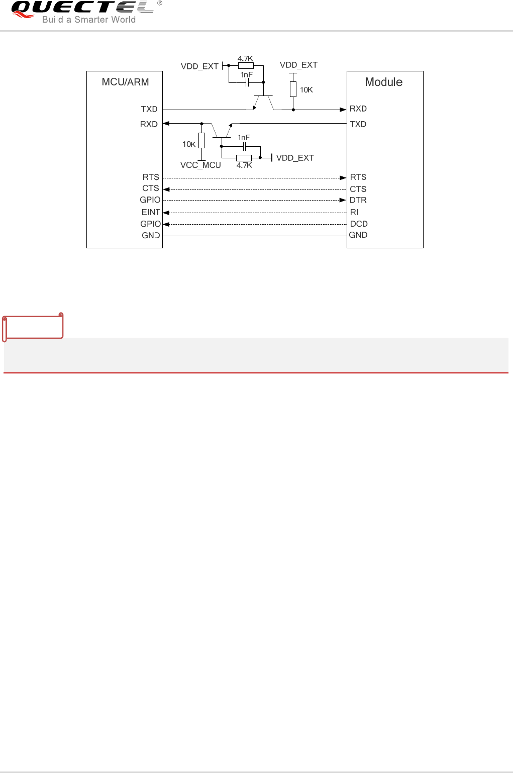
LTE Module Series
EC25 Hardware Design
EC25_Hardware_Design 53 / 112
Figure 21: Reference Circuit with Transistor Circuit
Transistor circuit solution is not suitable for applications with high baud rates exceeding 460Kbps.
3.12. PCM and I2C Interfaces
EC25 provides one Pulse Code Modulation (PCM) digital interface for audio design, which supports the
following modes and one I2C interface:
Primary mode (short frame synchronization, works as both master and slave)
Auxiliary mode (long frame synchronization, works as master only)
In primary mode, the data is sampled on the falling edge of the PCM_CLK and transmitted on the rising
edge. The PCM_SYNC falling edge represents the MSB. In this mode, the PCM interface supports
256kHz, 512kHz, 1024kHz or 2048kHz PCM_CLK at 8kHz PCM_SYNC, and also supports 4096kHz
PCM_CLK at 16kHz PCM_SYNC.
In auxiliary mode, the data is sampled on the falling edge of the PCM_CLK and transmitted on the rising
edge. The PCM_SYNC rising edge represents the MSB. In this mode, the PCM interface operates with a
256kHz, 512kHz, 1024kHz or 2048kHz PCM_CLK and an 8kHz, 50% duty cycle PCM_SYNC.
EC25 supports 16-bit linear data format. The following figures show the primary mode’s timing
relationship with 8KHz PCM_SYNC and 2048KHz PCM_CLK, as well as the auxiliary mode’s timing
relationship with 8KHz PCM_SYNC and 256KHz PCM_CLK.
NOTE
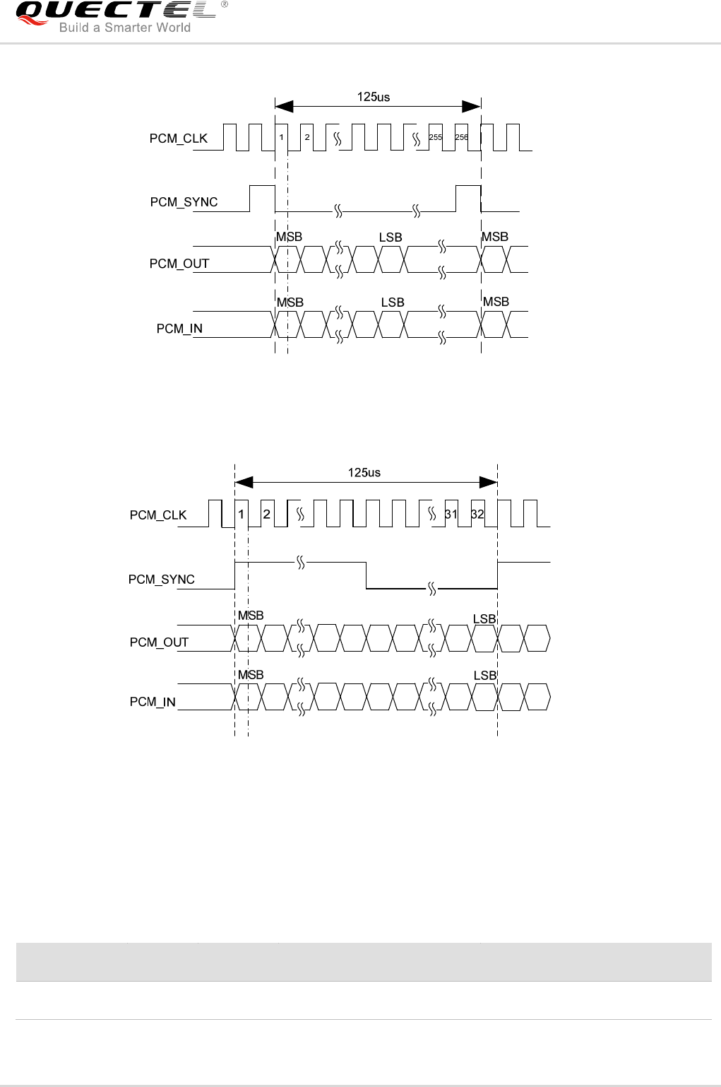
LTE Module Series
EC25 Hardware Design
EC25_Hardware_Design 54 / 112
Figure 22: Primary Mode Timing
Figure 23: Auxiliary Mode Timing
The following table shows the pin definition of PCM and I2C interfaces which can be applied on audio
codec design.
Table 14: Pin Definition of PCM and I2C Interfaces
Pin Name Pin No. I/O Description Comment
PCM_IN 24 DI PCM data input 1.8V power domain
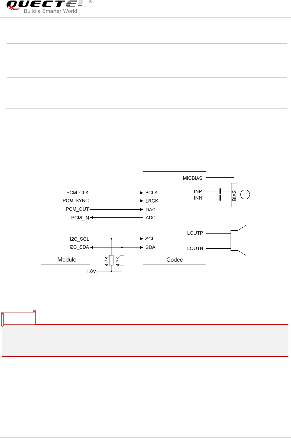
LTE Module Series
EC25 Hardware Design
EC25_Hardware_Design 55 / 112
Clock and mode can be configured by AT command, and the default configuration is master mode using
short frame synchronization format with 2048KHz PCM_CLK and 8KHz PCM_SYNC. Please refer to
document [2] for more details about AT+QDAI command.
The following figure shows a reference design of PCM interface with external codec IC.
Figure 24: Reference Circuit of PCM Application with Audio Codec
1. It is recommended to reserve an RC (R=22Ω, C=22pF) circuits on the PCM lines, especially for
PCM_CLK.
2. EC25 works as a master device pertaining to I2C interface.
PCM_OUT 25 DO PCM data output 1.8V power domain
PCM_SYNC 26 IO PCM data frame
synchronization signal 1.8V power domain
PCM_CLK 27 IO PCM data bit clock 1.8V power domain
I2C_SCL 41 OD I2C serial clock Require external pull-up to 1.8V
I2C_SDA 42 OD I2C serial data Require external pull-up to 1.8V
NOTES

LTE Module Series
EC25 Hardware Design
EC25_Hardware_Design 56 / 112
3.13. SD Card Interface
EC25 supports SDIO 3.0 interface for SD card.
The following table shows the pin definition of SD card interface.
Table 15: Pin Definition of SD Card Interface
Pin Name Pin No. I/O Description Comment
SDC2_DATA3 28 IO SD card SDIO bus DATA3
SDIO signal level can be
selected according to SD
card supported level,
please refer to SD 3.0
protocol for more details.
If unused, keep it open.
SDC2_DATA2 29 IO SD card SDIO bus DATA2
SDIO signal level can be
selected according to SD
card supported level,
please refer to SD 3.0
protocol for more details.
If unused, keep it open.
SDC2_DATA1 30 IO SD card SDIO bus DATA1
SDIO signal level can be
selected according to SD
card supported level,
please refer to SD 3.0
protocol for more details.
If unused, keep it open.
SDC2_DATA0 31 IO SD card SDIO bus DATA0
SDIO signal level can be
selected according to SD
card supported level,
please refer to SD 3.0
protocol for more details.
If unused, keep it open.
SDC2_CLK 32 DO SD card SDIO bus clock
SDIO signal level can be
selected according to SD
card supported level,
please refer to SD 3.0
protocol for more details.
If unused, keep it open.
SDC2_CMD 33 IO SD card SDIO bus command SDIO signal level can be
selected according to SD
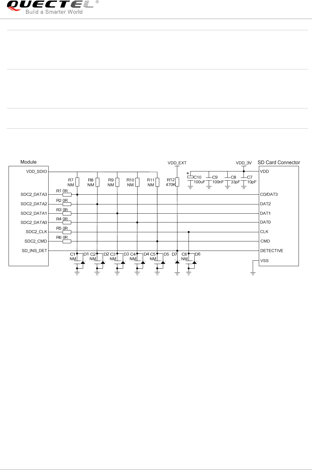
LTE Module Series
EC25 Hardware Design
EC25_Hardware_Design 57 / 112
The following figure shows a reference design of SD card.
Figure 25: Reference Circuit of SD card
In SD card interface design, in order to ensure good communication performance with SD card, the
following design principles should be complied with:
SD_INS_DET must be connected.
The voltage range of SD card power supply VDD_3V is 2.7V~3.6V and a sufficient current up to 0.8A
should be provided. As the maximum output current of VDD_SDIO is 50mA which can only be used
for SDIO pull-up resistors, an externally power supply is needed for SD card.
To avoid jitter of bus, resistors R7~R11 are needed to pull up the SDIO to VDD_SDIO. Value of these
resistors is among 10KΩ~100KΩ and the recommended value is 100KΩ. VDD_SDIO should be used
as the pull-up power.
In order to adjust signal quality, it is recommended to add 0Ω resistors R1~R6 in series between the
module and the SD card. The bypass capacitors C1~C6 are reserved and not mounted by default. All
resistors and bypass capacitors should be placed close to the module.
In order to offer good ESD protection, it is recommended to add a TVS diode on SD card pins near
the SD card connector with junction capacitance less than 15pF.
card supported level,
please refer to SD 3.0
protocol for more details.
If unused, keep it open.
VDD_SDIO 34 PO SD card SDIO bus pull up power
1.8V/2.85V configurable.
Cannot be used for SD
card power. If unused,
keep it open.
SD_INS_DET 23 DI SD card insertion detection 1.8V power domain.
If unused, keep it open.
LTE Module Series
EC25 Hardware Design
EC25_Hardware_Design 58 / 112
Keep SDIO signals far away from other sensitive circuits/signals such as RF circuits, analog signals,
etc., as well as noisy signals such as clock signals, DCDC signals, etc.
It is important to route the SDIO signal traces with total grounding. The impedance of SDIO data trace
is 50Ω (±10%).
Make sure the adjacent trace spacing is two times of the trace width and the load capacitance of
SDIO bus should be less than 15pF.
It is recommended to keep the trace length difference between CLK and DATA/CMD less than 1mm
and the total routing length less than 50mm. The total trace length inside the module is 27mm, so the
exterior total trace length should be less than 23mm.
3.14. ADC Interfaces
The module provides two analog-to-digital converter (ADC) interfaces. AT+QADC=0 command can be
used to read the voltage value on ADC0 pin. AT+QADC=1 command can be used to read the voltage
value on ADC1 pin. For more details about these AT commands, please refer to document [2].
In order to improve the accuracy of ADC, the trace of ADC should be surrounded by ground.
Table 16: Pin Definition of ADC Interfaces
The following table describes the characteristic of ADC function.
Table 17: Characteristic of ADC
Pin Name Pin No. Description
ADC0 45 General purpose analog to digital converter
ADC1 44 General purpose analog to digital converter
Parameter Min. Typ. Max. Unit
ADC0 Voltage Range 0.3 VBAT_BB V
ADC1 Voltage Range 0.3 VBAT_BB V
ADC Resolution 15 Bits
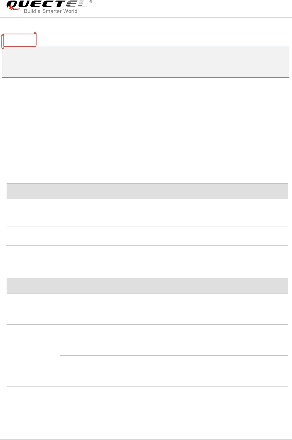
LTE Module Series
EC25 Hardware Design
EC25_Hardware_Design 59 / 112
1. ADC input voltage must not exceed VBAT_BB.
2. It is prohibited to supply any voltage to ADC pins when VBAT is removed.
3. It is recommended to use a resistor divider circuit for ADC application.
3.15. Network Status Indication
The network indication pins can be used to drive network status indication LEDs. The module provides
two pins which are NET_MODE and NET_STATUS. The following tables describe the pin definition and
logic level changes in different network status.
Table 18: Pin Definition of Network Connection Status/Activity Indicator
Table 19: Working State of the Network Connection Status/Activity Indicator
Pin Name Pin No. I/O Description Comment
NET_MODE 5 DO Indicate the module network
registration mode.
1.8V power domain
Cannot be pulled up
before startup
NET_STATUS 6 DO Indicate the module network activity
status. 1.8V power domain
Pin Name Logic Level Changes Network Status
NET_MODE
Always High Registered on LTE network
Always Low Others
NET_STATUS
Flicker slowly (200ms High/1800ms Low) Network searching
Flicker slowly (1800ms High/200ms Low) Idle
Flicker quickly (125ms High/125ms Low) Data transfer is ongoing
Always High Voice calling
NOTES
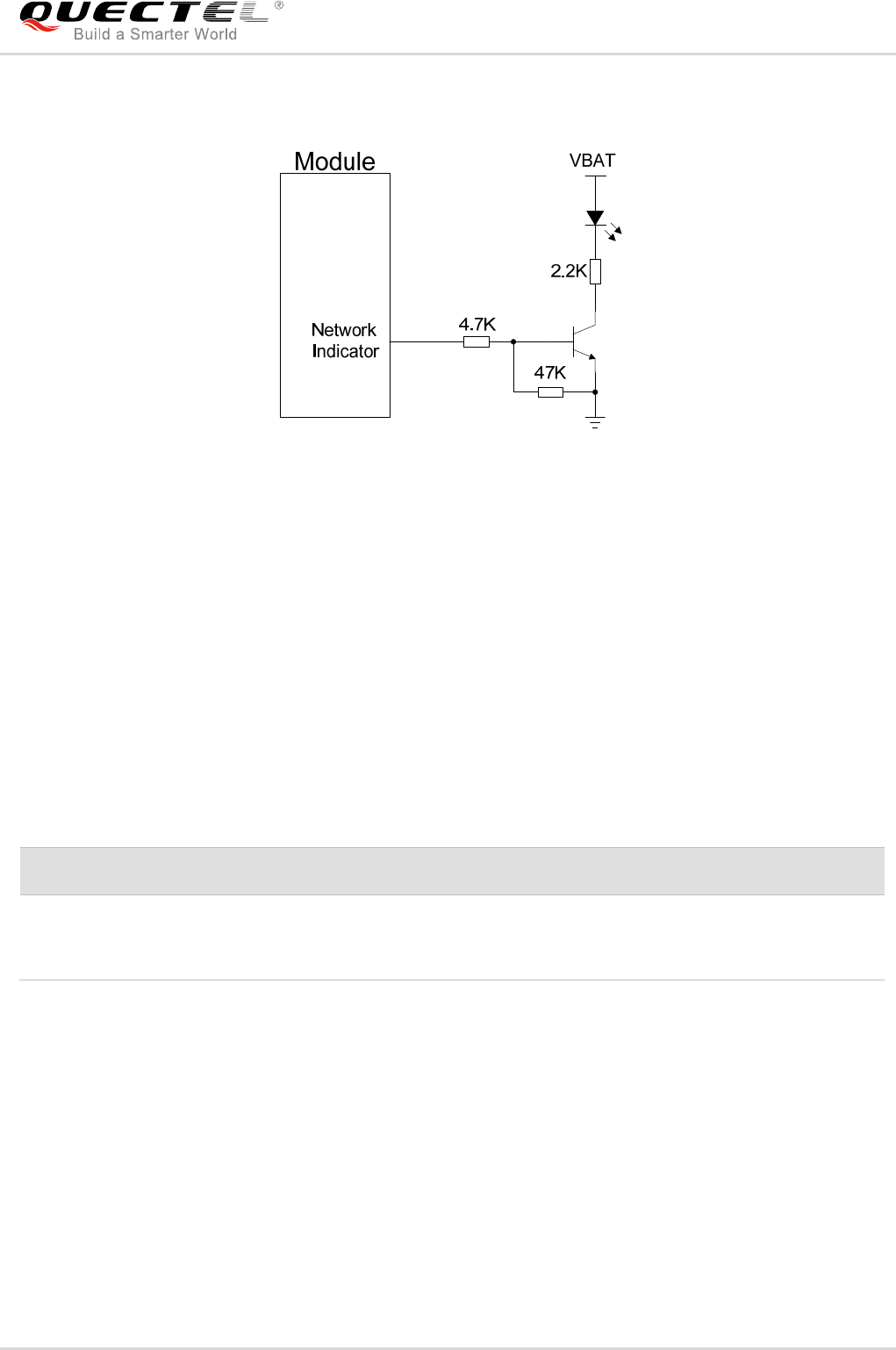
LTE Module Series
EC25 Hardware Design
EC25_Hardware_Design 60 / 112
A reference circuit is shown in the following figure.
Figure 26: Reference Circuit of the Network Indicator
3.16. STATUS
The STATUS pin is an open drain output for indicating the module’s operation status. It can be connected
to a GPIO of DTE with a pull-up resistor, or as LED indication circuit as below. When the module is turned
on normally, the STATUS will present the low state. Otherwise, the STATUS will present high-impedance
state.
Table 20: Pin Definition of STATUS
The following figure shows different circuit designs of STATUS, and customers can choose either one
according to customers’ application demands.
Pin Name Pin No. I/O Description Comment
STATUS 61 OD Indicate the module’s operation status
An external pull-up resistor
is required.
If unused, keep it open.
LTE Module Series
EC25 Hardware Design
EC25_Hardware_Design 61 / 112
Figure 27: Reference Circuits of STATUS
3.17. Behaviors of RI
AT+QCFG="risignaltype","physical" command can be used to configure RI behavior.
No matter on which port URC is presented, URC will trigger the behavior of RI pin.
URC can be outputted from UART port, USB AT port and USB modem port through configuration via
AT+QURCCFG command. The default port is USB AT port.
In addition, RI behavior can be configured flexibly. The default behavior of the RI is shown as below.
Table 21: Behavior of RI
The RI behavior can be changed by AT+QCFG="urc/ri/ring" command. Please refer to document [2]
for details.
State Response
Idle RI keeps at high level
URC RI outputs 120ms low pulse when a new URC returns
NOTE
LTE Module Series
EC25 Hardware Design
EC25_Hardware_Design 62 / 112
3.18. SGMII Interface
EC25 includes an integrated Ethernet MAC with an SGMII interface and two management interfaces, key
features of the SGMII interface are shown below:
IEEE802.3 compliance
Support 10M/100M/1000M Ethernet work mode
Support maximum 150Mbps (DL)/50Mbps (UL) for 4G network
Support VLAN tagging
Support IEEE1588 and Precision Time Protocol (PTP)
Can be used to connect to external Ethernet PHY like AR8033, or to an external switch
Management interfaces support dual voltage 1.8V/2.85V
The following table shows the pin definition of SGMII interface.
Table 22: Pin Definition of the SGMII Interface
Pin Name Pin No. I/O Description Comment
Control Signal Part
EPHY_RST_N 119 DO Ethernet PHY reset 1.8V/2.85V power domain
EPHY_INT_N 120 DI Ethernet PHY interrupt 1.8V power domain
SGMII_MDATA 121 IO SGMII MDIO (Management Data
Input/Output) data 1.8V/2.85V power domain
SGMII_MCLK 122 DO SGMII MDIO (Management Data
Input/Output) clock 1.8V/2.85V power domain
USIM2_VDD 128 PO SGMII MDIO pull-up power source
Configurable power source.
1.8V/2.85V power domain.
External pull-up power source for
SGMII MDIO pins.
SGMII Signal Part
SGMII_TX_M 123 AO SGMII transmission-minus Connect with a 0.1uF capacitor,
close to the PHY side.
SGMII_TX_P 124 AO SGMII transmission-plus Connect with a 0.1uF capacitor,
close to the PHY side.
SGMII_RX_P 125 AI SGMII receiving-plus Connect with a 0.1uF capacitor,
close to EC25 module.
SGMII_RX_M 126 AI SGMII receiving-minus Connect with a 0.1uF capacitor,
close to EC25 module.
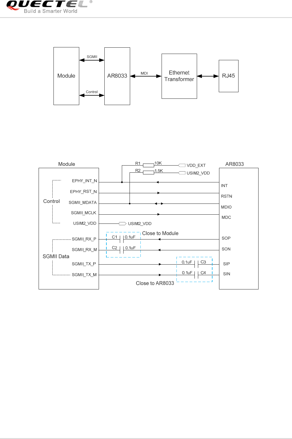
LTE Module Series
EC25 Hardware Design
EC25_Hardware_Design 63 / 112
The following figure shows the simplified block diagram for Ethernet application.
Figure 28: Simplified Block Diagram for Ethernet Application
The following figure shows a reference design of SGMII interface with PHY AR8033 application.
Figure 29: Reference Circuit of SGMII Interface with PHY AR8033 Application
In order to enhance the reliability and availability in customers’ applications, please follow the criteria
below in the Ethernet PHY circuit design:
Keep SGMII data and control signals away from other sensitive circuits/signals such as RF circuits,
analog signals, etc., as well as noisy signals such as clock signals, DCDC signals, etc.
Keep the maximum trace length less than 10-inch and keep skew on the differential pairs less than
20mil.
The differential impedance of SGMII data trace is 100Ω±10%, and the reference ground of the area
should be complete.
Make sure the trace spacing between SGMII RX and TX is at least 3 times of the trace width, and the
same to the adjacent signal traces.
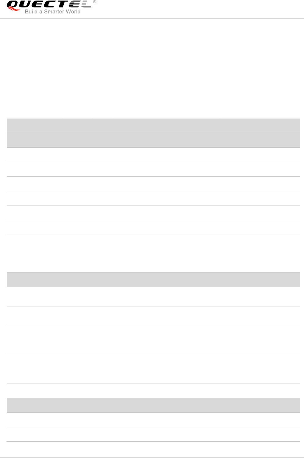
LTE Module Series
EC25 Hardware Design
EC25_Hardware_Design 64 / 112
3.19. Wireless Connectivity Interfaces
EC25 supports a low-power SDIO 3.0 interface for WLAN and a UART/PCM interface for BT.
The following table shows the pin definition of wireless connectivity interfaces.
Table 23: Pin Definition of Wireless Connectivity Interfaces
Pin Name Pin No. I/O Description Comment
WLAN Part
SDC1_DATA3 129 IO WLAN SDIO data bus D3 1.8V power domain
SDC1_DATA2 130 IO WLAN SDIO data bus D2 1.8V power domain
SDC1_DATA1 131 IO WLAN SDIO data bus D1 1.8V power domain
SDC1_DATA0 132 IO WLAN SDIO data bus D0 1.8V power domain
SDC1_CLK 133 DO WLAN SDIO bus clock 1.8V power domain
SDC1_CMD 134 IO WLAN SDIO bus command 1.8V power domain
WLAN_EN 136 DO
WLAN function control via FC20
module.
1.8V power domain.
Active high.
Cannot be pulled up
before startup.
Coexistence and Control Part
PM_ENABLE 127 DO External power control 1.8V power domain
Active high.
WAKE_ON_
WIRELESS 135 DI
Wake up the host (EC25 module) by
FC20 module 1.8V power domain
COEX_UART_RX 137 DI LTE/WLAN&BT coexistence signal
1.8V power domain.
Cannot be pulled up
before startup.
COEX_UART_TX 138 DO LTE/WLAN&BT coexistence signal
1.8V power domain.
Cannot be pulled up
before startup.
WLAN_SLP_CLK 118 DO WLAN sleep clock
BT Part*
BT_RTS* 37 DI BT UART request to send 1.8V power domain
BT_TXD* 38 DO BT UART transmit data 1.8V power domain
LTE Module Series
EC25 Hardware Design
EC25_Hardware_Design 65 / 112
The following figure shows a reference design of wireless connectivity interfaces with Quectel FC20
module.
Module
WAKE_ ON_WIRELESS
WLAN_SL P_CLK
PM_ENAB LE
DCDC/LDO
32K HZ_I N
WAKE_ ON_WIRELE SS
FC20 Module
VDD_3V3
POWER
SDC1_DATA3
SDC1_DATA2
SDC1_DATA1
SDC1_DATA0
SDC1_CLK
SDC1_CMD
WLAN_EN
SDIO_D3
SDIO_D2
SDIO_D1
SDIO_D0
SDIO_CLK
SDIO_CMD
WLAN_EN
WLAN
VDD_EXT VIO
COEX_UART_TX
COEX_ UART_RX LTE_UART_TXD
LTE_UART_RXD
COEX
Figure 30: Reference Circuit of Wireless Connectivity Interfaces with FC20 Module
1. FC20 module can only be used as a slave device.
2. When BT function is enabled on EC25 module, PCM_SYNC and PCM_CLK pins are only used to
output signals.
3. For more information about wireless connectivity interfaces, please refer to document [5].
BT_RXD* 39 DI BT UART receive data 1.8V power domain
BT_CTS* 40 DO BT UART clear to send
1.8V power domain.
Cannot be pulled up
before startup.
PCM_IN1) 24 DI PCM data input 1.8V power domain
PCM_OUT1) 25 DO PCM data output 1.8V power domain
PCM_SYNC1) 26 IO
PCM data frame synchronization
signal 1.8V power domain
PCM_CLK1) 27 IO PCM data bit clock 1.8V power domain
BT_EN* 139 DO BT function control via BT module. 1.8V power domain
Active high.
NOTES
LTE Module Series
EC25 Hardware Design
EC25_Hardware_Design 66 / 112
4. “*” means under development.
5. 1) Pads 24~27 are multiplexing pins used for audio design on EC25 module and BT function on BT
module.
3.19.1. WLAN Interface
EC25 provides a low power SDIO 3.0 interface and control interface for WLAN design.
SDIO interface supports the SDR mode (up to 50MHz).
As SDIO signals are very high-speed, in order to ensure the SDIO interface design corresponds with the
SDIO 3.0 specification, please comply with the following principles:
It is important to route the SDIO signal traces with total grounding. The impedance of SDIO signal
trace is 50Ω±10%.
Keep SDIO signals far away from other sensitive circuits/signals such as RF circuits, analog signals,
etc., as well as noisy signals such as clock signals, DCDC signals, etc.
It is recommended to keep matching length between CLK andDATA/CMD less than 1mm and total
routing length less than 50mm.
Keep termination resistors within 15Ω~24Ω on clock lines near the module and keep the route
distance from the module clock pins to termination resistors less than 5mm.
Make sure the adjacent trace spacing is 2 times of the trace width and bus capacitance is less than
15pF.
3.19.2. BT Interface*
EC25 supports a dedicated UART interface and a PCM interface for BT application.
Further information about BT interface will be added in future version of this document.
“*” means under development.
3.20. USB_BOOT Interface
EC25 provides a USB_BOOT pin. Developers can pull up USB_BOOT to VDD_EXT before powering on
the module, thus the module will enter into emergency download mode when powered on. In this mode,
the module supports firmware upgrade over USB interface.
NOTE
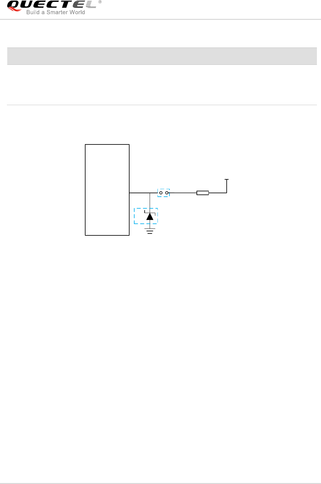
LTE Module Series
EC25 Hardware Design
EC25_Hardware_Design 67 / 112
Table 24: Pin Definition of USB_BOOT Interface
The following figure shows a reference circuit of USB_BOOT interface.
Module
USB_BOOT
VDD_EXT
4.7K
Test point
TVS
Close to test po int
Figure 31: Reference Circuit of USB_BOOT Interface
Pin Name Pin No. I/O Description Comment
USB_BOOT 115 DI Force the module enter into
emergency download mode
1.8V power domain.
Active high.
It is recommended to
reserve test point.

LTE Module Series
EC25 Hardware Design
EC25_Hardware_Design 68 / 112
4 GNSS Receiver
4.1. General Description
EC25 includes a fully integrated global navigation satellite system solution that supports Gen8C-Lite of
Qualcomm (GPS, GLONASS, BeiDou, Galileo and QZSS).
EC25 supports standard NMEA-0183 protocol, and outputs NMEA sentences at 1Hz data update rate via
USB interface by default.
By default, EC25 GNSS engine is switched off. It has to be switched on via AT command. For more
details about GNSS engine technology and configurations, please refer to document [3].
4.2. GNSS Performance
The following table shows GNSS performance of EC25.
Table 25: GNSS Performance
Parameter Description Conditions Typ. Unit
Sensitivity
(GNSS)
Cold start Autonomous -146 dBm
Reacquisition Autonomous -157 dBm
Tracking Autonomous -157 dBm
TTFF
(GNSS)
Cold start
@open sky
Autonomous 35 s
XTRA enabled 18 s
Warm start
@open sky
Autonomous 26 s
XTRA enabled 2.2 s
LTE Module Series
EC25 Hardware Design
EC25_Hardware_Design 69 / 112
1. Tracking sensitivity: the lowest GNSSsignal value at the antenna port on which the module can keep
on positioning for 3 minutes.
2. Reacquisition sensitivity: the lowest GNSS signal value at the antenna port on which the module can
fix position again within 3 minutes after loss of lock.
3. Cold start sensitivity: the lowest GNSS signal value at the antenna port on which the module fixes
position within 3 minutes after executing cold start command.
4.3. Layout Guidelines
The following layout guidelines should be taken into account in customers’ designs.
Maximize the distance among GNSS antenna, main antenna and Rx-diversity antenna.
Digital circuits such as (U)SIM card, USB interface, camera module and display connector should be
kept away from the antennas.
Use ground vias around the GNSS trace and sensitive analog signal traces to provide coplanar
isolation and protection.
Keep 50Ω characteristic impedance for the ANT_GNSS trace.
Please refer to Chapter 5 for GNSS antenna reference design and antenna installation information.
Hot start
@open sky
Autonomous 2.5 s
XTRA enabled 1.8 s
Accuracy
(GNSS) CEP-50 Autonomous
@open sky <1.5 m
NOTES
LTE Module Series
EC25 Hardware Design
EC25_Hardware_Design 70 / 112
5 Antenna Interfaces
EC25 antenna interfaces include a main antenna interface, an Rx-diversity antenna interface which is
used to resist the fall of signals caused by high speed movement and multipath effect, and a GNSS
antenna interface. The impedance of the antenna port is 50Ω.
5.1. Main/Rx-diversity Antenna Interfaces
5.1.1. Pin Definition
The pin definition of main antenna and Rx-diversityantenna interfaces is shown below.
Table 26: Pin Definition of RF Antenna
5.1.2. Operating Frequency
Table 27: Module Operating Frequencies
Pin Name Pin No. I/O Description Comment
ANT_MAIN 49 IO Main antenna pad 50Ω impedance
ANT_DIV 35 AI Receive diversity antenna pad
50Ω impedance
If unused, keep it
open.
3GPP Band Transmit Receive Unit
GSM850 824~849 869~894 MHz
EGSM900 880~915 925~960 MHz
DCS1800 1710~1785 1805~1880 MHz
PCS1900 1850~1910 1930~1990 MHz
WCDMA B1 1920~1980 2110~2170 MHz

LTE Module Series
EC25 Hardware Design
EC25_Hardware_Design 71 / 112
WCDMA B2 1850~1910 1930~1990 MHz
WCDMA B4 1710~1755 2110~2155 MHz
WCDMA B5 824~849 869~894 MHz
WCDMA B6 830~840 875~885 MHz
WCDMA B8 880~915 925~960 MHz
WCDMA B19 830~845 875~890 MHz
LTE FDD B1 1920~1980 2110~2170 MHz
LTE FDD B2 1850~1910 1930~1990 MHz
LTE FDD B3 1710~1785 1805~1880 MHz
LTE FDD B4 1710~1755 2110~2155 MHz
LTE FDD B5 824~849 869~894 MHz
LTE FDD B7 2500~2570 2620~2690 MHz
LTE FDD B8 880~915 925~960 MHz
LTE FDD B12 699~716 729~746 MHz
LTE FDD B13 777~787 746~756 MHZ
LTE FDD B14 788~798 758~768 MHZ
LTE FDD B18 815~830 860~875 MHz
LTE FDD B19 830~845 875~890 MHz
LTE FDD B20 832~862 791~821 MHz
LTE FDD B28 703~748 758~803 MHz
LTE TDD B38 2570~2620 2570~2620 MHz
LTE TDD B40 2300~2400 2300~2400 MHz
LTE TDD B41 2555~2655 2555~2655 MHz
LTE TDD B66 1710~1780 2100~2200 MHz
LTE TDD B71 663~698 617~652 MHz
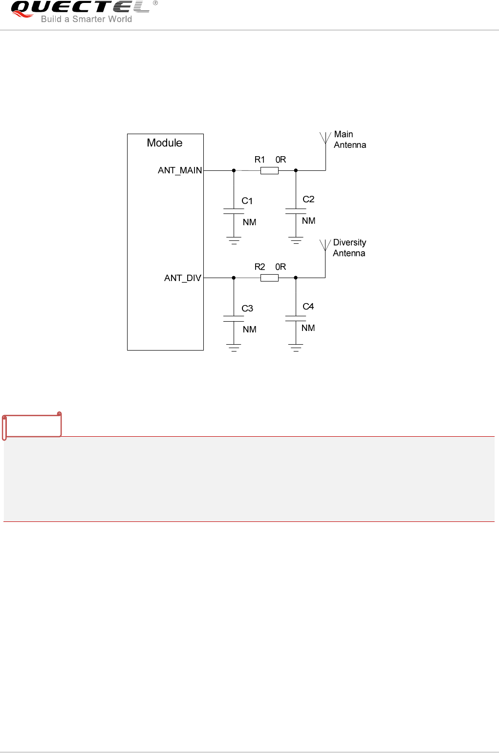
LTE Module Series
EC25 Hardware Design
EC25_Hardware_Design 72 / 112
5.1.3. Reference Design of RF Antenna Interface
Areference design of ANT_MAIN and ANT_DIV antenna pads is shown as below. A π-type matching
circuit should be reserved for better RF performance. The capacitors are not mounted by default.
Figure 32: Reference Circuit of RF Antenna Interface
1. Keep a proper distance between the main antenna and the Rx-diversity antenna to improve the
receiving sensitivity.
2. ANT_DIV function is enabled by default.
3. Place the π-type matching components (R1&C1&C2, R2&C3&C4) as close to the antenna as
possible.
5.1.4. Reference Design of RF Layout
For user’s PCB, the characteristic impedance of all RF traces should be controlled as 50Ω. The
impedance of the RF traces is usually determined by the trace width (W), the materials’ dielectric constant,
the distance between signal layer and reference ground (H), and the clearance between RF trace and
ground (S). Microstrip line or coplanar waveguide line is typically used in RF layout for characteristic
impedance control. The following are reference designs of microstrip line or coplanar waveguide line with
different PCB structures
NOTES
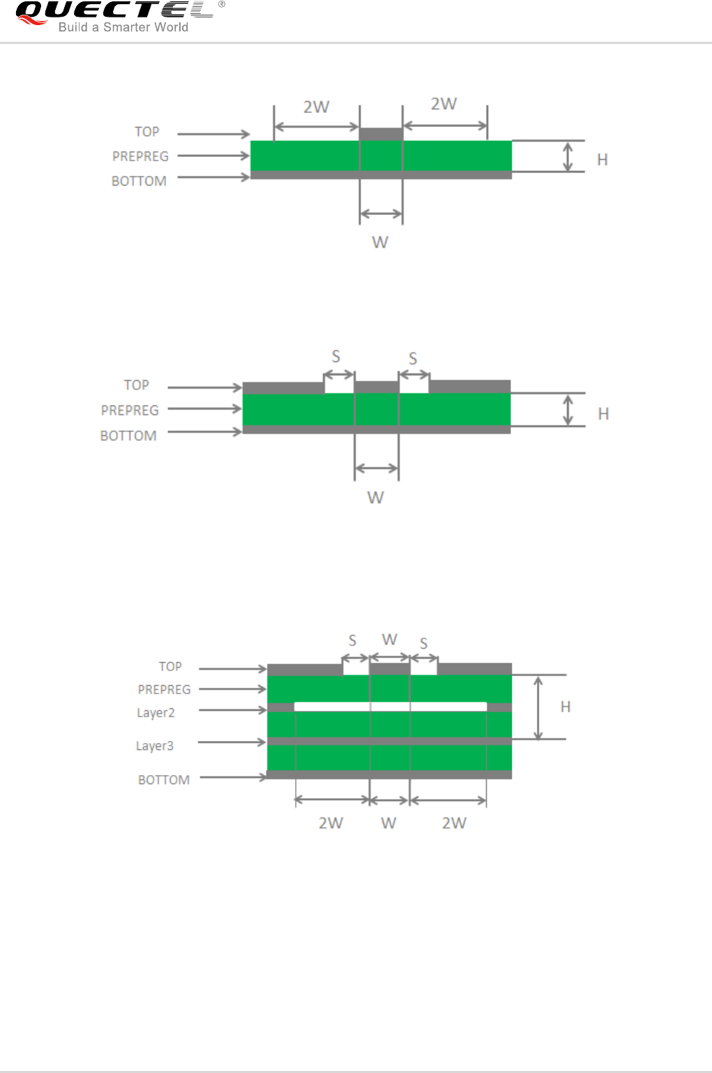
LTE Module Series
EC25 Hardware Design
EC25_Hardware_Design 73 / 112
.
Figure 33: Microstrip Line Design on a 2-layer PCB
Figure 34: Coplanar Waveguide Line Design on a 2-layer PCB
Figure 35: Coplanar Waveguide Line Design on a 4-layer PCB (Layer 3 as Reference Ground)
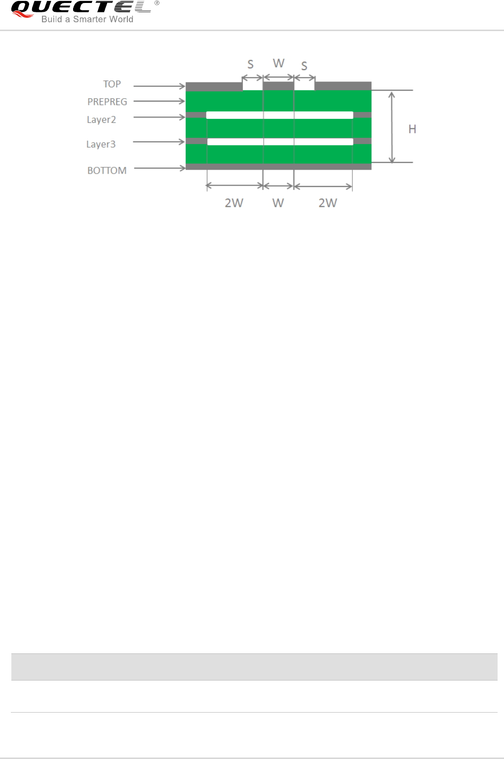
LTE Module Series
EC25 Hardware Design
EC25_Hardware_Design 74 / 112
Figure 36: Coplanar Waveguide Line Design on a 4-layer PCB (Layer 4 as Reference Ground)
In order to ensure RF performance and reliability, the following principles should be complied with in RF
layout design:
Please use an impedance simulation tool to control the characteristic impedance of RF traces as
50Ω.
The GND pins adjacent to RF pins should not be designed as thermal relief pads, and they should be
fully connected to ground.
The distance between the RF pins and the RF connector should be as short as possible, and all the
right angle traces should be changed to curved ones.
There should be clearance area under the signal pin of the antenna connector or solder joint.
The reference ground of RF traces should be complete. Meanwhile, adding some ground vias around
RF traces and the reference ground could help to improve RF performance. The distance between
the ground vias and RF traces should be no less than two times the width of RF signal traces (2*W).
For more details about RF layout, please refer to document [6].
5.2. GNSS Antenna Interface
The following tables show pin definition and frequency specification of GNSS antenna interface.
Table 28: Pin Definition of GNSS Antenna Interface
Pin Name Pin No. I/O Description Comment
ANT_GNSS 47 AI GNSS antenna 50Ω impedance
If unused, keep it open.
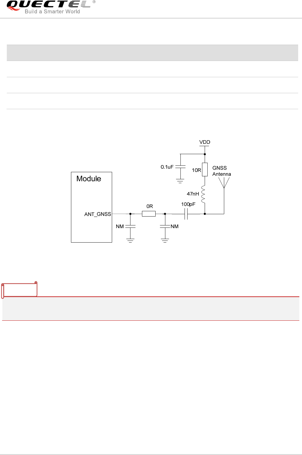
LTE Module Series
EC25 Hardware Design
EC25_Hardware_Design 75 / 112
Table 29: GNSS Frequency
A reference design of GNSS antenna is shown as below.
Figure 37: Reference Circuit of GNSS Antenna
1. An external LDO can be selected to supply power according to the active antenna requirement.
2. If the module is designed with a passive antenna, then the VDD circuit is not needed.
Type Frequency Unit
GPS/Galileo/QZSS 1575.42±1.023 MHz
GLONASS 1597.5~1605.8 MHz
BeiDou 1561.098±2.046 MHz
NOTES
LTE Module Series
EC25 Hardware Design
EC25_Hardware_Design 76 / 112
5.3. Antenna Installation
5.3.1. Antenna Requirement
The following table shows the requirements on main antenna, Rx-diversity antenna and GNSS antenna.
Table 30: Antenna Requirements
1) It is recommended to use a passive GNSS antenna when LTE B13 or B14 is supported, as the use of
active antenna may generate harmonics which will affect the GNSS performance.
Type Requirements
GNSS1)
Frequency range: 1561MHz~1615MHz
Polarization: RHCP or linear
VSWR: < 2 (Typ.)
Passive antenna gain: > 0dBi
Active antenna noise figure: < 1.5dB
Active antenna gain: > 0dBi
Active antenna embedded LNA gain: < 17 dB
GSM/WCDMA/LTE
VSWR: ≤ 2
Efficiency: > 30%
Max Input Power: 50W
Input Impedance: 50Ω
Cable Insertion Loss: < 1dB
(GSM850, GSM 900, WCDMA B5/B6/B8/B19,
LTE-FDD B5/B8/B12/B13/B14/B18/B19/B20/B26/B28/B71)
Cable Insertion Loss: < 1.5dB
(DCS1800, PCS1900, WCDMA B1/B2/B4,
LTE-FDD B1/B2/B3/B4/B66)
Cable Insertion loss: < 2dB
(LTE-FDD B7, LTE-TDD B38/B40/B41)
NOTE
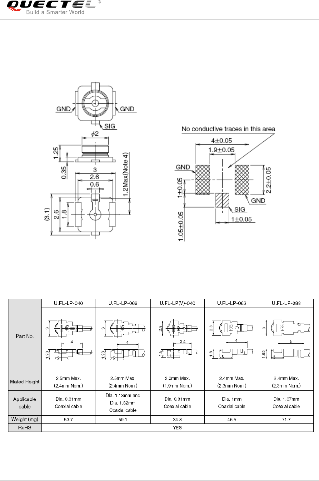
LTE Module Series
EC25 Hardware Design
EC25_Hardware_Design 77 / 112
5.3.2. Recommended RF Connector for Antenna Installation
If RF connector is used for antenna connection, it is recommended to use U.FL-R-SMT connector
provided by Hirose.
Figure 38: Dimensions of the U.FL-R-SMT Connector (Unit: mm)
U.FL-LP serial connectors listed in the following figure can be used to match the U.FL-R-SMT.
Figure 39: Mechanicals of U.FL-LP Connectors
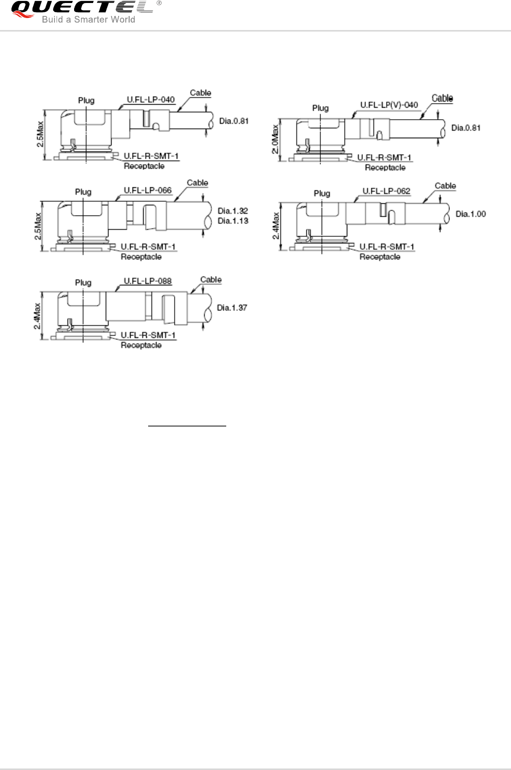
LTE Module Series
EC25 Hardware Design
EC25_Hardware_Design 78 / 112
The following figure describes the space factor of mated connector.
Figure 40: Space Factor of Mated Connector (Unit: mm)
For more details, please visit http://hirose.com.

LTE Module Series
EC25 Hardware Design
EC25_Hardware_Design 79 / 112
6 Electrical, Reliability and Radio
Characteristics
6.1. Absolute Maximum Ratings
Absolute maximum ratings for power supply and voltage on digital and analog pins of the module are
listed in the following table.
Table 31: Absolute Maximum Ratings
Parameter Min. Max. Unit
VBAT_RF/VBAT_BB -0.3 4.7 V
USB_VBUS -0.3 5.5 V
Peak Current of VBAT_BB 0 0.8 A
Peak Current of VBAT_RF 0 1.8 A
Voltage at Digital Pins -0.3 2.3 V
Voltage at ADC0 0 VBAT_BB V
Voltage at ADC1 0 VBAT_BB V
LTE Module Series
EC25 Hardware Design
EC25_Hardware_Design 80 / 112
6.2. Power Supply Ratings
Table 32: The Module Power Supply Ratings
6.3. Operation and Storage Temperatures
The operation and storage temperatures are listed in the following table.
Table 33: Operation and Storage Temperatures
1. 1) Within operation temperature range, the module is 3GPP compliant.
2. 2) Within extended temperature range, the module remains the ability to establish and maintain a
voice, SMS, data transmission, emergency call, etc. There is no unrecoverable malfunction. There
are also no effects on radio spectrum and no harm to radio network. Only one or more parameters
like Pout might reduce in their value and exceed the specified tolerances. When the temperature
Parameter Description Conditions Min. Typ. Max. Unit
VBAT
VBAT_BB and
VBAT_RF
The actual input voltages
must stay between the
minimum and maximum
values.
3.3 3.8 4.3 V
Voltage drop during
burst transmission
Maximum power control
level on EGSM900. 400 mV
IVBAT
Peak supply current
(during transmission
slot)
Maximum power control
level on EGSM900. 1.8 2.0 A
USB_VBUS USB detection 3.0 5.0 5.25 V
Parameter Min. Typ. Max. Unit
OperationTemperature Range1) -35 +25 +75 ºC
Extended Operation Range2) -40 +85 ºC
Storage Temperature Range -40 +90 ºC
NOTES

LTE Module Series
EC25 Hardware Design
EC25_Hardware_Design 81 / 112
returns to the normal operating temperature levels, the module will meet 3GPP specifications again.
6.4. Current Consumption
The values of current consumption are shown below.
Table 34: EC25-E Current Consumption
Parameter Description Conditions Typ. Unit
IVBAT
OFF state Power down 11 uA
Sleep state
AT+CFUN=0 (USB disconnected) 1.16 mA
GSM DRX=2 (USB disconnected) 2.74 mA
GSM DRX=9 (USB disconnected) 2.0 mA
WCDMA PF=64 (USB disconnected) 2.15 mA
WCDMA PF=128 (USB disconnected) 1.67 mA
LTE-FDD PF=64 (USB disconnected) 2.60 mA
LTE-FDD PF=128 (USB disconnected) 1.90 mA
LTE-TDD PF=64 (USB disconnected) 2.79 mA
LTE-TDD PF=128 (USB disconnected) 2.00 mA
Idle state
GSM DRX=5 (USB disconnected) 19.5 mA
GSM DRX=5 (USB connected) 29.5 mA
WCDMA PF=64 (USB disconnected) 21.0 mA
WCDMA PF=64 (USB connected) 31.0 mA
LTE-FDD PF=64 (USB disconnected) 20.7 mA
LTE-FDD PF=64 (USB connected) 30.8 mA
LTE-TDD PF=64 (USB disconnected) 20.8 mA

LTE Module Series
EC25 Hardware Design
EC25_Hardware_Design 82 / 112
LTE-TDD PF=64 (USB connected) 32.0 mA
GPRS data
transfer
(GNSS OFF)
EGSM900 4DL/1UL @33.22dBm 271.0 mA
EGSM900 3DL/2UL @33.0dBm 464.0 mA
EGSM900 2DL/3UL @30.86dBm 524.0 mA
EGSM900 1DL/4UL @29.58dBm 600 mA
DCS1800 4DL/1UL @29.92dBm 192.0 mA
DCS1800 3DL/2UL @29.84dBm 311.0 mA
DCS1800 2DL/3UL @29.67dBm 424.0 mA
DCS1800 1DL/4UL @29.48dBm 539.0 mA
EDGE data
transfer
(GNSS OFF)
EGSM900 4DL/1UL PCL=8 @27.40dBm 174.0 mA
EGSM900 3DL/2UL PCL=8 @27.24dBm 281.0 mA
EGSM900 2DL/3UL PCL=8 @27.11dBm 379.0 mA
EGSM900 1DL/4UL PCL=8 @26.99dBm 480.0 mA
DCS1800 4DL/1UL PCL=2 @25.82dBm 159.0 mA
DCS1800 3DL/2UL PCL=2 @25.85dBm 251.0 mA
DCS1800 2DL/3UL PCL=2 @25.68dBm 340.0 mA
DCS1800 1DL/4UL PCL=2 @25.57dBm 433.0 mA
WCDMA
datatransfer
(GNSS OFF)
WCDMA B1 HSDPA @22.47dBm 613.0 mA
WCDMA B1 HSUPA @22.44dBm 609.0 mA
WCDMA B5 HSDPA @23.07dBm 671.0 mA
WCDMA B5 HSUPA @23.07dBm 669.0 mA
WCDMA B8 HSDPA @22.67dBm 561.0 mA
WCDMA B8 HSUPA @22.39dBm 557.0 mA
LTE datatransfer
(GNSS OFF)
LTE-FDD B1 @23.27dBm 754.0 mA
LTE-FDD B3 @23.54dBm 774.0 mA
LTE Module Series
EC25 Hardware Design
EC25_Hardware_Design 83 / 112
Table 35: EC25-A Current Consumption
LTE datatransfer
(GNSS OFF)
LTE-FDD B5 @22.83dBm 762.0 mA
LTE-FDD B7 @23.37dBm 842.0 mA
LTE-FDD B8 @23.48dBm 720.0 mA
LTE-FDD B20 @22.75dBm 714.0 mA
LTE-TDD B38 @23.05dBm 481.0 mA
LTE-TDD B40 @23.17dBm 431.8 mA
LTE-TDD B41 @23.02dBm 480.0 mA
GSM
voice call
EGSM900 PCL=5 @33.08dBm 264.0 mA
DCS1800 PCL=0 @29.75dBm 190.0 mA
WCDMA voice
call
WCDMA B1 @23.22dBm 680.0 mA
WCDMA B5 @23.18dBm 677.0 mA
WCDMA B8 @23.54dBm 618.0 mA
Parameter Description Conditions Typ. Unit
IVBAT
OFF state Power down 10 uA
Sleep state
AT+CFUN=0 (USB disconnected) 1.1 mA
WCDMA PF=64 (USB disconnected) 1.8 mA
WCDMA PF=128 (USB disconnected) 1.5 mA
LTE-FDD PF=64 (USB disconnected) 2.2 mA
LTE-FDD PF=128 (USB disconnected) 1.6 mA
Idle state
WCDMA PF=64 (USB disconnected) 21.0 mA
WCDMA PF=64 (USB connected) 31.0 mA
LTE-FDD PF=64 (USB disconnected) 21.0 mA
LTE-FDD PF=64 (USB connected) 31.0 mA

LTE Module Series
EC25 Hardware Design
EC25_Hardware_Design 84 / 112
Table 36: EC25-V Current Consumption
WCDMA
datatransfer
(GNSS OFF)
WCDMA B2 HSDPA @21.9dBm 591.0 mA
WCDMA B2 HSUPA @21.62dBm 606.0 mA
WCDMA B4 HSDPA @22.02dBm 524.0 mA
WCDMA B4 HSUPA @21.67dBm 540.0 mA
WCDMA B5 HSDPA @22.71dBm 490.0 mA
WCDMA B5 HSUPA @22.58dBm 520.0 mA
LTE datatransfer
(GNSS OFF)
LTE-FDD B2 @22.93dBm 715.0 mA
LTE-FDD B4 @22.96dBm 738.0 mA
LTE-FDD B12 @23.35dBm 663.0 mA
WCDMA voice
call
WCDMA B2 @22.93dBm 646.0 mA
WCDMA B4 @23dBm 572.0 mA
WCDMA B5 @23.78dBm 549.0 mA
Parameter Description Conditions Typ. Unit
IVBAT
OFF state Power down 10 uA
Sleep state
AT+CFUN=0 (USB disconnected) 0.85 mA
LTE-FDD PF=64 (USB disconnected) 2.0 mA
LTE-FDD PF=128 (USB disconnected) 1.5 mA
Idle state
LTE-FDD PF=64 (USB disconnected) 20.0 mA
LTE-FDD PF=64 (USB connected) 31.0 mA
WCDMA B2 HSUPA @21.62dBm 606.0 mA
WCDMA B4 HSDPA @22.02dBm 524.0 mA
WCDMA B4 HSUPA @21.67dBm 540.0 mA
WCDMA B5 HSDPA @22.71dBm 490.0 mA
LTE Module Series
EC25 Hardware Design
EC25_Hardware_Design 85 / 112
Table 37: EC25-J Current Consumption
WCDMA B5 HSUPA @22.58dBm 520.0 mA
LTE
datatransfer
(GNSS OFF)
LTE-FDD B4 @23.14dBm 770.0 mA
LTE-FDD B13 @23.48dBm 531.0 mA
Parameter Description Conditions Typ. Unit
IVBAT
OFF state Power down 10 uA
Sleep state
AT+CFUN=0 (USB disconnected) 1.1 mA
WCDMA PF=64 (USB disconnected) 1.9 mA
WCDMA PF=128 (USB disconnected) 1.5 mA
LTE-FDD PF=64 (USB disconnected) 2.5 mA
LTE-FDD PF=128 (USB disconnected) 1.8 mA
LTE-TDD PF=64 (USB disconnected) 2.6 mA
LTE-TDD PF=128 (USB disconnected) 1.9 mA
Idle state
WCDMA PF=64 (USB disconnected) 21.0 mA
WCDMA PF=64 (USB connected) 31.0 mA
LTE-FDD PF=64 (USB disconnected) 21.0 mA
LTE-FDD PF=64 (USB connected) 32.0 mA
LTE-TDD PF=64 (USB disconnected) 21.0 mA
LTE-TDD PF=64 (USB connected) 32.0 mA
WCDMA
datatransfer
(GNSS OFF)
WCDMA B1 HSDPA @22.32dBm 550.0 mA
WCDMA B1 HSUPA @22.64dBm 516.0 mA
WCDMA B6 HSDPA @22.02dBm 524.0 mA
WCDMA B6 HSUPA @22.33dBm 521.0 mA
WCDMA B19 HSDPA @22.67dBm 517.0 mA
LTE Module Series
EC25 Hardware Design
EC25_Hardware_Design 86 / 112
Table 38: EC25-AU Current Consumption
WCDMA B19 HSUPA @22.33dBm 522.0 mA
LTE
datatransfer
(GNSS OFF)
LTE-FDD B1 @23.16dBm 685.0 mA
LTE-FDD B3 @23.22dBm 766.0 mA
LTE-FDD B8 @23.22dBm 641.0 mA
LTE-FDD B18 @23.35dBm 661.0 mA
LTE-FDD B19 @23.16dBm 677.0 mA
LTE-FDD B26 @22.87dBm 690.0 mA
LTE-TDD B41 @22.42dBm 439.0 mA
WCDMA voice
call
WCDMA B1 @22.33dBm 605.0 mA
WCDMA B6 @23.28dBm 549.0 mA
WCDMA B19 @23.28dBm 549.0 mA
Parameter Description Conditions Typ. Unit
IVBAT
OFF state Power down 11 uA
Sleep state
AT+CFUN=0 1.3 mA
AT+CFUN=0 (USB disconnected) 1.46 mA
GSM850 DRX=5 (USB disconnected) 1.8 mA
EGSM900 DRX=5 (USB disconnected) 2.0 mA
DCS1800 DRX=5 (USB disconnected) 1.9 mA
PCS1900 DRX=5 (USB disconnected) 1.9 mA
WCDMA PF=64 (USB disconnected) 2.0 mA
WCDMA PF=128 (USB disconnected) 1.6 mA
LTE-FDD PF=64 (USB disconnected) 2.2 mA
LTE-FDD PF=128 (USB disconnected) 1.6 mA

LTE Module Series
EC25 Hardware Design
EC25_Hardware_Design 87 / 112
LTE-TDD PF=64 (USB disconnected) 2.3 mA
LTE-TDD PF=128 (USB disconnected) 1.6 mA
Idle state
EGSM900 DRX=5 (USB disconnected) 22.0 mA
EGSM900 DRX=5 (USB connected) 34.0 mA
WCDMA PF=64 (USB disconnected) 22.0 mA
WCDMA PF=64 (USB connected) 33.0 mA
LTE-FDD PF=64 (USB disconnected) 24.0 mA
LTE-FDD PF=64 (USB connected) 35.0 mA
LTE-TDD PF=64 (USB disconnected) 24.0 Ma
LTE-TDD PF=64 (USB connected) 35.0 mA
GPRS data
transfer
(GNSS OFF)
GSM850 1UL/4DL @32.53dBm 232.0 mA
GSM850 2UL/3DL @32.34dBm 384.0 mA
GSM850 3UL/2DL @30.28dBm 441.0 mA
GSM850 4UL/1DL @29.09dBm 511.0 mA
EGSM900 1UL/4DL @32.34dBm 241.0 mA
EGSM900 2UL/3DL @32.19dBm 397.0 mA
EGSM900 3UL/2DL @30.17dBm 459.0 mA
EGSM900 4UL/1DL @28.96dBm 533.0 mA
DCS1800 1UL/4DL @29.71dBm 183.0 mA
DCS1800 2UL/3DL @29.62dBm 289.0 mA
DCS1800 3UL/2DL @29.49dBm 392.0 mA
DCS1800 4UL/1DL @29.32dBm 495.0 mA
PCS1900 1UL/4DL @29.61dBm 174.0 mA
PCS1900 1UL/4DL @29.48dBm 273.0 mA
PCS1900 1UL/4DL @29.32dBm 367.0 mA

LTE Module Series
EC25 Hardware Design
EC25_Hardware_Design 88 / 112
PCS1900 1UL/4DL @29.19dBm 465.0 mA
EDGE data
transfer
(GNSS OFF)
GSM850 1UL/4DL @27.09dBm 154.0 mA
GSM850 2UL/3DL @26.94dBm 245.0 mA
GSM850 3UL/2DL @26.64dBm 328.0 mA
GSM850 4UL/1DL @26.53dBm 416.0 mA
EGSM900 1UL/4DL @26.64dBm 157.0 mA
EGSM900 2UL/3DL @26.95dBm 251.0 mA
EGSM900 3UL/2DL @26.57dBm 340.0 mA
EGSM900 4UL/1DL @26.39dBm 431.0 mA
DCS18001 UL/4DL @26.03dBm 152.0 mA
DCS1800 2UL/3DL @25.62dBm 240.0 mA
DCS1800 3UL/2DL @25.42dBm 325.0 mA
DCS1800 4UL/1DL @25.21dBm 415.0 mA
PCS1900 1UL/4DL @25.65dBm 148.0 mA
PCS1900 1UL/4DL @25.63dBm 232.0 mA
PCS1900 1UL/4DL @25.54dBm 313.0 mA
PCS1900 1UL/4DL @25.26dBm 401.0 mA
WCDMA data
(GNSS OFF)
WCDMA B1 HSDPA @22.34dBm 625.0 mA
WCDMA B1 HSUPA @21.75dBm 617.0 mA
WCDMA B2 HSDPA @22.51dBm 610.0 mA
WCDMA B2 HSUPA @22. 14dBm 594.0 mA
WCDMA B5 HSDPA @22.98dBm 576.0 mA
WCDMA B5 HSUPA @22.89dBm 589.0 mA
WCDMA B8 HSDPA @22.31dBm 556.0 mA
WCDMA B8 HSUPA @22.11dBm 572.0 mA

LTE Module Series
EC25 Hardware Design
EC25_Hardware_Design 89 / 112
Table 39: EC25-AUT Current Consumption
LTE
datatransfer
(GNSS OFF)
LTE-FDD B1 @23.28dBm 817.0 mA
LTE-FDD B2 @23.34dBm 803.0 mA
LTE-FDD B3 @23.2dBm 785.0 mA
LTE-FDD B4 @22.9dBm 774.0 mA
LTE-FDD B5 @23.45dBm 687.0 mA
LTE-FDD B7 @22.84dBm 843.0 mA
LTE-FDD B8 @22.92dBm 689.0 mA
LTE-FDD B28 @23.23dBm 804.0 mA
LTE-TDD B40 @23.3dBm 429.0 mA
GSM voice
call
GSM850 PCL5 @32.66dBm 228.0 mA
EGSM900 PCL5 @32.59dBm 235.0 mA
DCS1800 PCL0 @29.72dBm 178.0 mA
PCS1900 PCL0 @29.82dBm 170.0 mA
WCDMA
voice call
WCDMA B1 @23.27dBm 687.0 mA
WCDMA B2 @23.38dBm 668.0 mA
WCDMA B5 @23.38dBm 592.0 mA
WCDMA B8 @23.32dBm 595.0 mA
Parameter Description Conditions Typ. Unit
IVBAT
OFF state Power down 10 uA
Sleep state
AT+CFUN=0 (USB disconnected) 1.0 mA
WCDMA PF=64 (USB disconnected) 1.9 mA
WCDMA PF=128 (USB disconnected) 1.5 mA
LTE-FDD PF=64 (USB disconnected) 2.3 mA
LTE-FDD PF=128 (USB disconnected) 1.9 mA
LTE Module Series
EC25 Hardware Design
EC25_Hardware_Design 90 / 112
Table 40: EC25-AF Current Consumption
IVBAT
Idle state
WCDMA PF=64 (USB disconnected) 23.0 mA
WCDMA PF=64 (USB connected) 33.0 mA
LTE-FDD PF=64 (USB disconnected) 17.0 mA
LTE-FDD PF=64 (USB connected) 29.0 mA
LTE-TDD PF=64 (USB disconnected) 21.0 mA
LTE-TDD PF=64 (USB connected) 32.0 mA
WCDMA
datatransfer
(GNSS OFF)
WCDMA B1 HSDPA @22.24dBm 500.0 mA
WCDMA B1 HSUPA @22.05dBm 499.0 mA
WCDMA B5 HSDPA @22.39dBm 418.0 mA
WCDMA B5 HSUPA @22dBm 486.0 mA
LTE
datatransfer
(GNSS OFF)
LTE-FDD B1 @23.28dBm 707.0 mA
LTE-FDD B3 @23.36dBm 782.0 mA
LTE-FDD B5 @23.32dBm 588.0 mA
LTE-FDD B7 @23.08dBm 692.0 mA
LTE-FDD B28-A @23.37dBm 752.0 mA
LTE-FDD B28-B @23.48dBm 770.0 mA
WCDMA voice
call
WCDMA B1 @23.22dBm 546.0 mA
WCDMA B5 @23.01dBm 511.0 mA
Parameter Description Conditions Typ. Unit
IVBAT
OFF state Power down 10 uA
Sleep state
AT+CFUN=0 (USB disconnected) 1.0 mA
WCDMA PF=64 (USB disconnected) 1.8 mA
WCDMA PF=128 (USB disconnected) 1.4 mA

LTE Module Series
EC25 Hardware Design
EC25_Hardware_Design 91 / 112
IVBAT
LTE-FDD PF=64 (USB disconnected) 2.2 mA
LTE-FDD PF=128 (USB disconnected) 1.8 mA
Idle state
WCDMA PF=64 (USB disconnected) 23.3 mA
WCDMA PF=64 (USB connected) 33.4 mA
LTE-FDD PF=64 (USB disconnected) 17.6 mA
LTE-FDD PF=64 (USB connected) 29.4 mA
WCDMA
datatransfer
(GNSS OFF)
WCDMA B2 HSDPA @22.36dBm 509.0 mA
WCDMA B2 HSUPA @22.27dBm 511.0 mA
WCDMA B4 HSDPA @22.22dBm 521.0 mA
WCDMA B4 HSUPA @22.31dBm 518.0 mA
WCDMA B5 HSDPA @22.39dBm 496.0 mA
WCDMA B5 HSUPA @22dBm 502.0 mA
LTE
datatransfer
(GNSS OFF)
LTE-FDD B2 @23.2dBm 600.0 mA
LTE-FDD B4 @23.85dBm 634.0 mA
LTE-FDD B5 @23.0dBm 600.0 mA
LTE-FDD B12 @23.08dBm 692.0 mA
LTE-FDD B13 @23.1dBm 660.0 mA
LTE-FDD B14 @23.5dBm 676.0 mA
LTE-FDD B66 @22.9dBm 662.0 mA
LTE-FDD B71 @22.88dBm 600.0 mA
WCDMA voice
call
WCDMA B2 @23.24dBm 570.0 mA
WCDMA B4 @23.2dBm 581.0 mA
WCDMA B5 @23.4dBm 500.0 mA
LTE Module Series
EC25 Hardware Design
EC25_Hardware_Design 92 / 112
Table 41: GNSS Current Consumption of EC25 Series Module
6.5. RF Output Power
The following table shows the RF output power of EC25 module.
Table 42: RF Output Power
In GPRS 4 slots TX mode, the maximum output power is reduced by 3dB. The design conforms to the
GSM specification as described in Chapter 13.16 of 3GPP TS 51.010-1.
Parameter Description Conditions Typ. Unit
IVBAT
(GNSS)
Searching
(AT+CFUN=0)
Cold start @Passive Antenna 54.0 mA
Lost state @Passive Antenna 53.9 mA
Tracking
(AT+CFUN=0)
Instrument Environment 30.5 mA
Open Sky @Passive Antenna 33.2 mA
Open Sky @Active Antenna 40.8 mA
Frequency Max. Min.
GSM850/EGSM900 33dBm±2dB 5dBm±5dB
DCS1800/PCS1900 30dBm±2dB 0dBm±5dB
GSM850/EGSM900 (8-PSK) 27dBm±3dB 5dBm±5dB
DCS1800/PCS1900 (8-PSK) 26dBm±3dB 0dBm±5dB
WCDMA bands 24dBm+1/-3dB <-49dBm
LTE-FDD bands 23dBm±2dB <-39dBm
LTE-TDD bands 23dBm±2dB <-39dBm
NOTE
LTE Module Series
EC25 Hardware Design
EC25_Hardware_Design 93 / 112
6.6. RF Receiving Sensitivity
The following tables show conducted RF receiving sensitivity of EC25 series module.
Table 43: EC25-E Conducted RF Receiving Sensitivity
Table 44: EC25-A Conducted RF Receiving Sensitivity
Frequency Primary Diversity SIMO1) 3GPP (SIMO)
EGSM900 -109.0dBm / / -102.0dBm
DCS1800 -109.0dBm / / -102.0dbm
WCDMA B1 -110.5dBm / / -106.7dBm
WCDMA B5 -110.5dBm / / -104.7dBm
WCDMA B8 -110.5dBm / / -103.7dBm
LTE-FDD B1 (10M) -98.0dBm -98.0dBm -101.5dBm -96.3dBm
LTE-FDD B3 (10M) -96.5dBm -98.5dBm -101.5dBm -93.3dBm
LTE-FDD B5 (10M) -98.0dBm -98.5dBm -101.0dBm -94.3dBm
LTE-FDD B7 (10M) -97.0dBm -94.5dBm -99.5dBm -94.3dBm
LTE-FDD B8 (10M) -97.0dBm -97.0dBm -101.0dBm -93.3dBm
LTE-FDD B20 (10M) -97.5dBm -99.0dBm -102.5dBm -93.3dBm
LTE-TDD B38 (10M) -96.7dBm -97.0dBm -100.0dBm -96.3dBm
LTE-TDD B40 (10M) -96.3dBm -98.0dBm -101.0dBm -96.3dBm
LTE-TDD B41 (10M) -95.2dBm -95.7dBm -99.0dBm -94.3dBm
Frequency Primary Diversity SIMO1) 3GPP (SIMO)
WCDMA B2 -110.0dBm / / -104.7dBm
WCDMA B4 -110.0dBm / / -106.7dBm
WCDMA B5 -110.5dBm / / -104.7dBm
LTE Module Series
EC25 Hardware Design
EC25_Hardware_Design 94 / 112
Table 45: EC25-V Conducted RF Receiving Sensitivity
Table 46: EC25-J Conducted RF Receiving Sensitivity
LTE-FDD B2 (10M) -98.0dBm -98.0dBm -101.0dBm -94.3dBm
LTE-FDD B4 (10M) -97.5dBm -99.0dBm -101.0dBm -96.3dBm
LTE-FDD B12 (10M) -96.5dBm -98.0dBm -101.0dBm -93.3dBm
Frequency Primary Diversity SIMO1) 3GPP (SIMO)
LTE-FDD B4 (10M) -97.5dBm -99.0dBm -101.0dBm -96.3dBm
LTE-FDD B13 (10M) -95.0dBm -97.0dBm -100.0dBm -93.3dBm
Frequency Primary Diversity SIMO1) 3GPP (SIMO)
WCDMA B1 -110.0dBm / / -106.7dBm
WCDMA B6 -110.5dBm / / -106.7dBm
WCDMA B8 -110.5dBm / / -103.7dBm
WCDMA B19 -110.5dBm / / -106.7dBm
LTE-FDD B1 (10M) -97.5dBm -98.7dBm -100.2dBm -96.3dBm
LTE-FDD B3 (10M) -96.5dBm -97.1dBm -100.5dBm -93.3dBm
LTE-FDD B8 (10M) -98.4dBm -99.0dBm -101.2dBm -93.3dBm
LTE-FDD B18 (10M) -99.5dBm -99.0dBm -101.7dBm -96.3dBm
LTE-FDD B19 (10M) -99.2dBm -99.0dBm -101.4dBm -96.3dBm
LTE-FDD B26 (10M) -99.5dBm -99.0dBm -101.5dBm -93.8dBm
LTE-TDD B41 (10M) -95.0dBm -95.7dBm -99.0dBm -94.3dBm
LTE Module Series
EC25 Hardware Design
EC25_Hardware_Design 95 / 112
Table 47: EC25-AU Conducted RF Receiving Sensitivity
Table 48: EC25-AUT Conducted RF Receiving Sensitivity
Frequency Primary Diversity SIMO1) 3GPP (SIMO)
WCDMA B1 -110.0dBm / / -106.7dBm
WCDMA B5 -110.5dBm / / -104.7dBm
LTE-FDD B1 (10M) -98.5dBm -98.0dBm -101.0dBm -96.3dBm
Frequency Primary Diversity SIMO1) 3GPP (SIMO)
GSM850 -109.0dBm / / -102.0dBm
EGSM900 -109.0dBm / / -102.0dBm
DCS1800 -109.0dBm / / -102.0dBm
PCS1900 -109.0dBm / / -102.0dBm
WCDMA B1 -110.0dBm / / -106.7dBm
WCDMA B2 -110.0dBm / / -104.7dBm
WCDMA B5 -111.0dBm / / -104.7dBm
WCDMA B8 -111.0dBm / / -103.7dBm
LTE-FDD B1 (10M) -97.2dBm -97.5dBm -100.2dBm -96.3dBm
LTE-FDD B2 (10M) -98.2dBm / / -94.3dBm
LTE-FDD B3 (10M) -98.7dBm -98.6dBm -102.2dBm -93.3dBm
LTE-FDD B4 (10M) -97.7dBm -97.4dBm -100.2dBm -96.3dBm
LTE-FDD B5 (10M) -98.0dBm -98.2dBm -101.0dBm -94.3dBm
LTE-FDD B7 (10M) -97.7dBm -97.7dBm -101.2dBm -94.3dBm
LTE-FDD B8 (10M) -99.2dBm -98.2dBm -102.2dBm -93.3dBm
LTE-FDD B28 (10M) -98.6dBm -98.7dBm -102.0dBm -94.8dBm
LTE-TDD B40 (10M) -97.2dBm -98.4dBm -101.2dBm -96.3dBm

LTE Module Series
EC25 Hardware Design
EC25_Hardware_Design 96 / 112
LTE-FDD B3 (10M) -98.0dBm -96.0dBm -100.0dBm -93.3dBm
LTE-FDD B5 (10M) -98.0dBm -99.0dBm -102.5dBm -94.3dBm
LTE-FDD B7 (10M) -97.0dBm -95.0dBm -98.5dBm -94.3dBm
LTE-FDD B28 (10M) -97.0dBm -99.0dBm -102.0dBm -94.8dBm
Table 49: EC25-AUTL Conducted RF Receiving Sensitivity
Table 50: EC25-AF Conducted RF Receiving Sensitivity
Frequency Primary Diversity SIMO1) 3GPP (SIMO)
LTE-FDD B3 (10M) -98.0dBm -96.0dBm -100.0dBm -93.3dBm
LTE-FDD B7 (10M) -97.0dBm -95.0dBm -98.5dBm -94.3dBm
LTE-FDD B28 (10M) -97.0dBm -99.0dBm -102.0dBm -94.8dBm
Frequency Primary Diversity SIMO1) 3GPP (SIMO)
WCDMA B2 -109.5dBm -111dbm -113dbm -104.7dBm
WCDMA B4 -108dBm -111dbm -111.5dbm -106.7dBm
WCDMA B5 -110.5dBm -111.5dbm -114dbm -104.7dBm
LTE-FDD B2 (10M) -98.2dBm -99.1dBm -101.7dBm -94.3dBm
LTE-FDD B4 (10M) -97.3dBm -98.6dBm -101.1dBm -96.3dBm
LTE-FDD B5 (10M) -99dBm -100.3dBm -101.3dBm -94.3Bm
LTE-FDD B12 (10M) -99dBm -99.2dBm -102.1dBm -93.3dBm
LTE-FDD B13 (10M) -98.1dBm -98.4dBm -100.2dBm -93.3dBm
LTE-FDD B14 (10M) -97.9dBm -98.6dBm -99.5dBm -93.3dBm
LTE-FDD B66 (10M) -96.7dBm -98.1dBm -99.4dBm -96.5dBm
LTE-FDD B71 (10M) -99.2dBm -99.4dBm -101.5dBm -94.2dBm
LTE Module Series
EC25 Hardware Design
EC25_Hardware_Design 97 / 112
1) SIMO is a smart antenna technology that uses a single antenna at the transmitter side and two
antennas at the receiver side, which can improve RX performance.
6.7. Electrostatic Discharge
The module is not protected against electrostatics discharge (ESD) in general. Consequently, it is subject
to ESD handling precautions that typically apply to ESD sensitive components. Proper ESD handling and
packaging procedures must be applied throughout the processing, handling and operation of any
application that incorporates the module.
The following table shows the module electrostatics discharge characteristics.
Table 51: Electrostatics Discharge Characteristics
6.8. Thermal Consideration
In order to achieve better performance of the module, it is recommended to comply with the following
principles for thermal consideration:
On customers’ PCB design, please keep placement of the module away from heating sources,
especially high power components such as ARM processor, audio power amplifier, power supply,
etc.
Do not place components on the opposite side of the PCB area where the module is mounted, in
order to facilitate adding of heatsink when necessary.
Do not apply solder mask on the opposite side of the PCB area where the module is mounted, so as
to ensure better heat dissipation performance.
The reference ground of the area where the module is mounted should be complete, and add ground
vias as many as possible for better heat dissipation.
Make sure the ground pads of the module and PCB are fully connected.
Tested Points Contact Discharge Air Discharge Unit
VBAT, GND ±5 ±10 kV
All Antenna Interfaces ±4 ±8 kV
Other Interfaces ±0.5 ±1 kV
NOTE
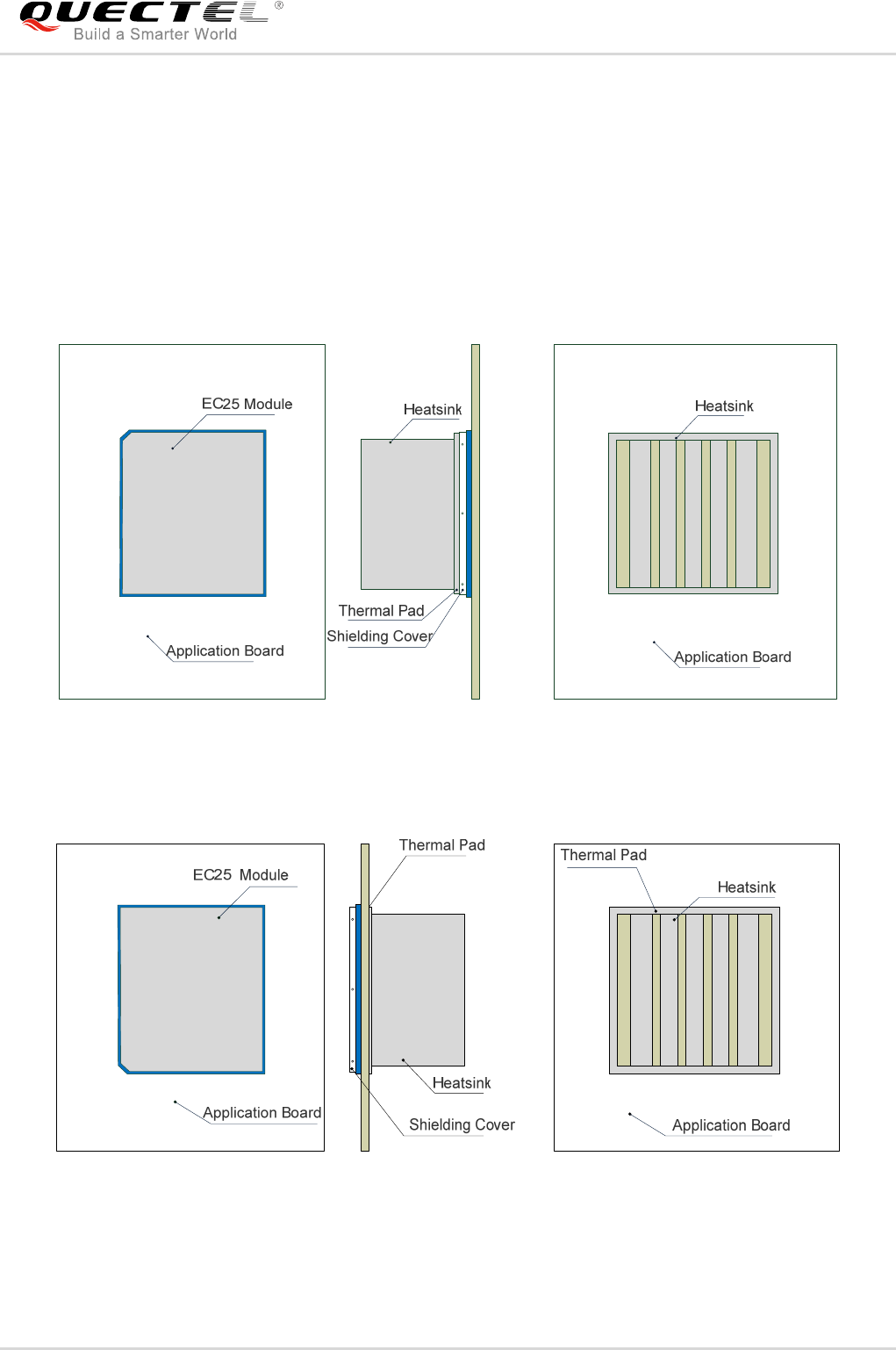
LTE Module Series
EC25 Hardware Design
EC25_Hardware_Design 98 / 112
According to customers’ application demands, the heatsink can be mounted on the top of the module,
or the opposite side of the PCB area where the module is mounted, or both of them.
The heatsink should be designed with as many fins as possible to increase heat dissipation area.
Meanwhile, a thermal pad with high thermal conductivity should be used between the heatsink and
module/PCB.
The following shows two kinds of heatsink designs for reference and customers can choose one or both
of them according to their application structure.
Figure 41: Referenced Heatsink Design (Heatsink at the Top of the Module)
Figure 42: Referenced Heatsink Design (Heatsink at the Backside of Customers’ PCB)

LTE Module Series
EC25 Hardware Design
EC25_Hardware_Design 99 / 112
The module offers the best performance when the internal BB chip stays below 105°C. When the
maximum temperature of the BB chip reaches or exceeds 105°C, the module works normal but provides
reduced performance (such as RF output power, data rate, etc.). When the maximum BB chip
temperature reaches or exceeds 115°C, the module will disconnect from the network, and it will recover to
network connected state after the maximum temperature falls below 115°C. Therefore, the thermal design
should be maximally optimized to make sure the maximum BB chip temperature always maintains below
105°C. Customers can execute AT+QTEMP command and get the maximum BB chip temperature from
the first returned value.
NOTE
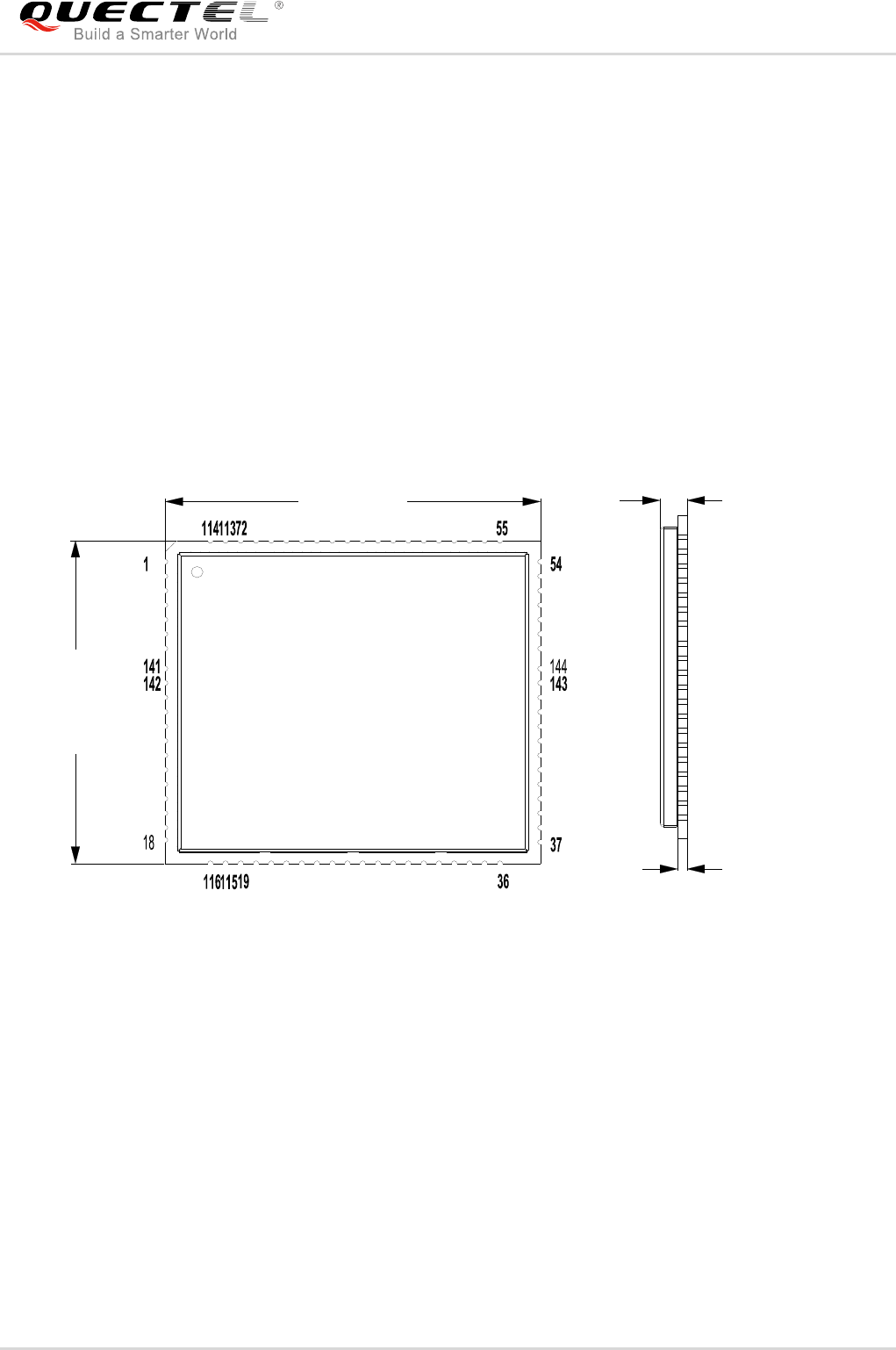
LTE Module Series
EC25 Hardware Design
EC25_Hardware_Design 100 / 112
7 Mechanical Dimensions
This chapter describes the mechanical dimensions of the module. All dimensions are measured in mm.
The tolerances for dimensions without tolerance values are ±0.05mm.
7.1. Mechanical Dimensions of the the Module
32.0±0.15
29.0±0.15
0.8
2.4±0.2
Figure 43: Module Top and Side Dimensions
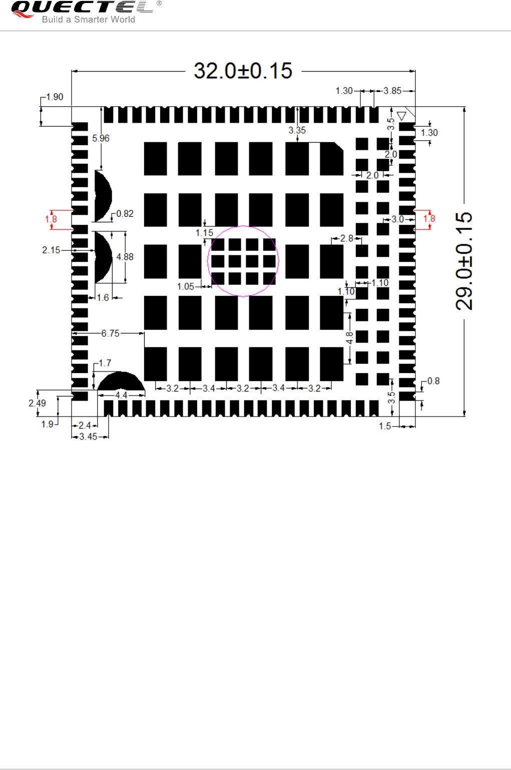
LTE Module Series
EC25 Hardware Design
EC25_Hardware_Design 101 / 112
Figure 44: Module Bottom Dimensions (Bottom View)
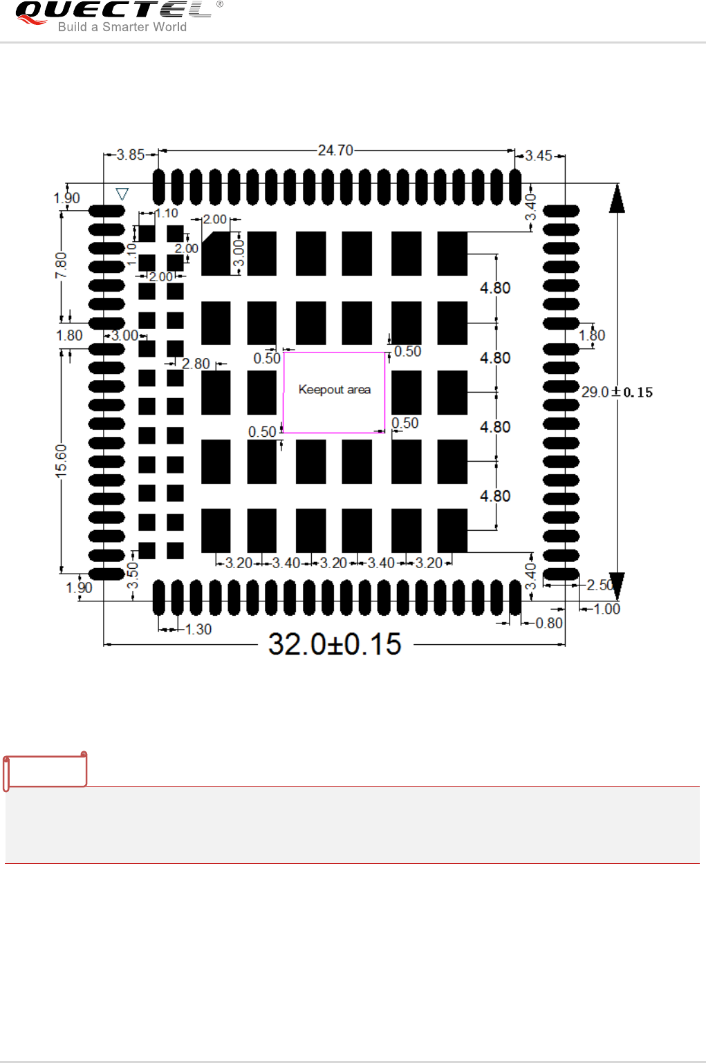
LTE Module Series
EC25 Hardware Design
EC25_Hardware_Design 102 / 112
7.2. Recommended Footprint
Figure 45: Recommended Footprint (Top View)
1. The keepout area should not be designed.
2. For easy maintenance of the module, please keep about 3mm between the module and other
components in thehost PCB.
NOTES
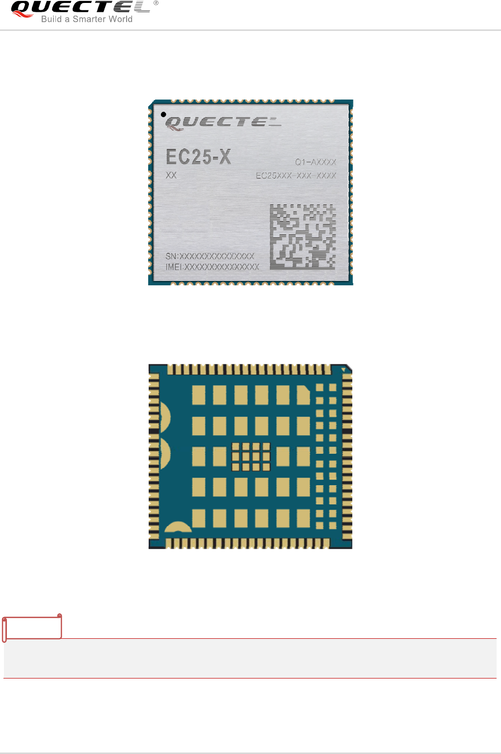
LTE Module Series
EC25 Hardware Design
EC25_Hardware_Design 103 / 112
7.3. Design Effect Drawings of the Module
Figure 46: Top View of the Module
Figure 47: Bottom View of the Module
These are design effect drawings of EC25 module. For more accurate pictures, please refer to the
module that you get from Quectel.
NOTE
LTE Module Series
EC25 Hardware Design
EC25_Hardware_Design 104 / 112
8 Storage, Manufacturing and
Packaging
8.1. Storage
EC25 is stored in a vacuum-sealed bag. It is rated at MSL 3, and its storage restrictions are listed below.
1. Shelf life in vacuum-sealed bag: 12 months at <40ºC/90%RH.
2. After the vacuum-sealed bag is opened, devices that will be subjected to reflow soldering or other
high temperature processes must be:
Mounted within 168 hours at the factory environment of ≤30ºC/60%RH.
Stored at <10% RH.
3. Devices require bake before mounting, if any circumstances below occurs:
When the ambient temperature is 23ºC±5ºC and the humidity indicator card shows the humidity
is >10% before opening the vacuum-sealed bag.
Device mounting cannot be finished within 168 hours at factory conditions of ≤30ºC/60%RH.
4. If baking is required, devices may be baked for 8 hours at 120ºC±5ºC.
As the plastic packagecannot be subjected to high temperature, it should be removed from devices before
high temperature (120ºC) baking. If shorter baking time is desired, please refer to IPC/JEDECJ-STD-033
for baking procedure.
NOTE
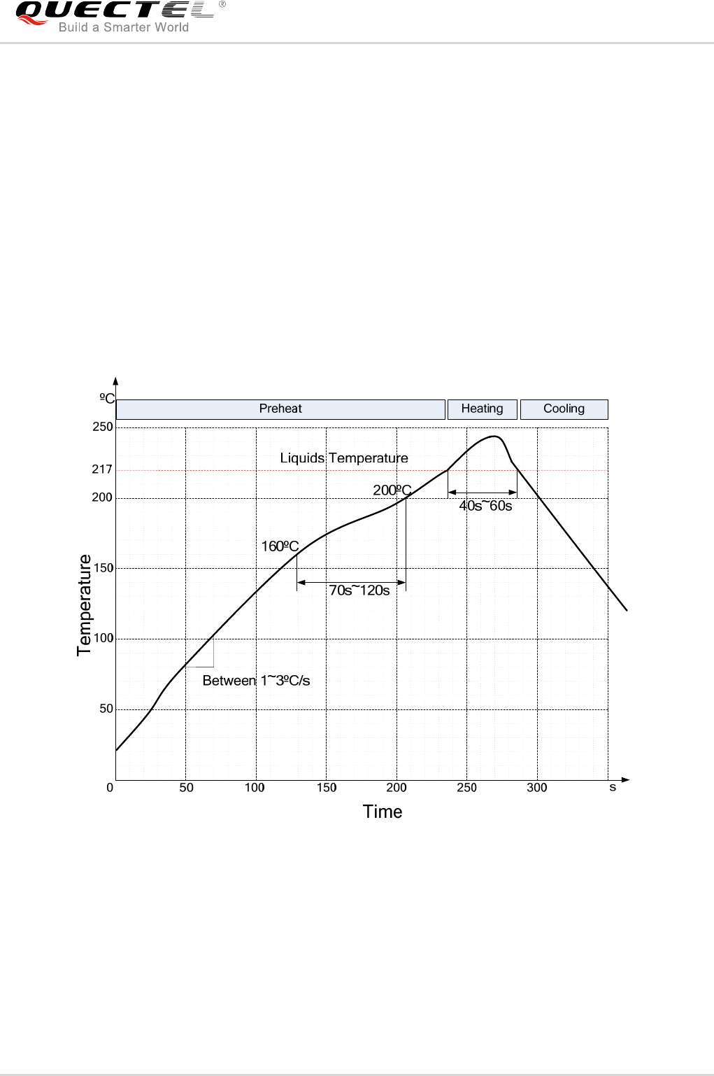
LTE Module Series
EC25 Hardware Design
EC25_Hardware_Design 105 / 112
8.2. Manufacturing and Soldering
Push the squeegee to apply the solder paste on the surface of stencil, thus making the paste fill the
stencil openings and then penetrate to the PCB. The force on the squeegee should be adjusted
properlyso as to produce a clean stencil surface on a single pass. To ensure the module soldering quality,
thethickness of stencil for the module is recommended to be 0.20mm. For more details, please refer to
document [4].
It is suggested that the peak reflow temperature is 235ºC~245ºC (for SnAg3.0Cu0.5 alloy). The absolute
maximum reflow temperature is 260ºC. To avoid damage to the module caused by repeated heating, it is
suggested that the module should be mounted after reflow soldering for the other side of PCB has been
completed. Recommended reflow soldering thermal profile is shown below:
Figure 48: Reflow Soldering Thermal Profile
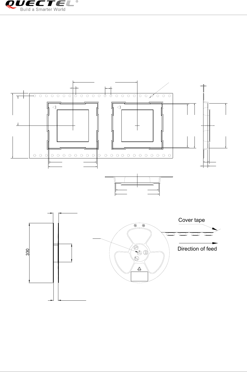
LTE Module Series
EC25 Hardware Design
EC25_Hardware_Design 106 / 112
8.3. Packaging
EC25 is packaged in tap andreel carriers. One reel is 11.88m long and contains 250pcs modules. The
figure below shows the package details, measured in mm.
30.3±0.15
29.3±0.15
30.3±0.15
32.5±0.15
33.5±0.15
0.35± 0.05
4.2±0.15
3.1±0.15
32.5± 0.15
33.5± 0.15
4.00±0.1
2.00±0.1
1.75±0.1
20.20±0.15
44.00±0.3
44.00±0.1
1.50±0.1
13
100
44.5+0.20
-0.00
48.5
Figure 49: Tape and Reel Specifications
LTE Module Series
EC25 Hardware Design
EC25_Hardware_Design 107 / 112
9 Appendix A References
Table 52: Related Documents
Table 53: Terms and Abbreviations
SN Document Name Remark
[1] Quectel_EC2x&EG9x&EM05_Power_Management_
Application_Note
Power management application notefor
EC25, EC21, EC20 R2.0, EC20 R2.1,
EG95, EG91 and EM05 modules
[2] Quectel_EC25&EC21_AT_Commands_Manual EC25 and EC21 AT commands manual
[3] Quectel_EC25&EC21_GNSS_AT_Commands_
Manual
EC25 and EC21 GNSS AT commands
manual
[4] Quectel_Module_Secondary_SMT_User_Guide Module secondary SMT user guide
[5] Quectel_EC25_Reference_Design EC25 reference design
[6] Quectel_RF_Layout_Application_Note RF layout application note
Abbreviation Description
AMR Adaptive Multi-rate
bps Bits Per Second
CHAP Challenge Handshake Authentication Protocol
CS Coding Scheme
CSD Circuit Switched Data
CTS Clear To Send
DC-HSPA+ Dual-carrier High Speed Packet Access
DFOTA Delta Firmware Upgrade Over The Air

LTE Module Series
EC25 Hardware Design
EC25_Hardware_Design 108 / 112
DL Downlink
DTR Data Terminal Ready
DTX Discontinuous Transmission
EFR Enhanced Full Rate
ESD Electrostatic Discharge
FDD Frequency Division Duplex
FR Full Rate
GLONASS GLObalnaya NAvigatsionnaya Sputnikovaya Sistema, the Russian Global
Navigation Satellite System
GMSK Gaussian Minimum Shift Keying
GNSS Global Navigation Satellite System
GPS Global Positioning System
GSM Global System for Mobile Communications
HR Half Rate
HSPA High Speed Packet Access
HSDPA High Speed Downlink Packet Access
HSUPA High Speed Uplink Packet Access
I/O Input/Output
Inorm Normal Current
LED Light Emitting Diode
LNA Low Noise Amplifier
LTE Long Term Evolution
MIMO Multiple Input Multiple Output
MO Mobile Originated
MS Mobile Station (GSM engine)
MT Mobile Terminated

LTE Module Series
EC25 Hardware Design
EC25_Hardware_Design 109 / 112
PAP Password Authentication Protocol
PCB Printed Circuit Board
PDU Protocol Data Unit
PPP Point-to-Point Protocol
QAM Quadrature Amplitude Modulation
QPSK Quadrature Phase Shift Keying
RF Radio Frequency
RHCP Right Hand Circularly Polarized
Rx Receive
SIM Subscriber Identification Module
SIMO Single Input Multiple Output
SMS Short Message Service
TDD Time Division Duplexing
TDMA Time Division Multiple Access
TD-SCDMA Time Division-Synchronous Code Division Multiple Access
TX Transmitting Direction
UL Uplink
UMTS Universal Mobile Telecommunications System
URC Unsolicited Result Code
USIM Universal Subscriber Identity Module
Vmax Maximum Voltage Value
Vnorm Normal Voltage Value
Vmin Minimum Voltage Value
VIHmax Maximum Input High Level Voltage Value
VIHmin Minimum Input High Level Voltage Value

LTE Module Series
EC25 Hardware Design
EC25_Hardware_Design 110 / 112
VILmax Maximum Input Low Level Voltage Value
VILmin Minimum Input Low Level Voltage Value
VImax Absolute Maximum Input Voltage Value
VImin Absolute Minimum Input Voltage Value
VOHmax Maximum Output High Level Voltage Value
VOHmin Minimum Output High Level Voltage Value
VOLmax Maximum Output Low Level Voltage Value
VOLmin Minimum Output Low Level Voltage Value
VSWR Voltage Standing Wave Ratio
WCDMA Wideband Code Division Multiple Access
WLAN Wireless Local Area Network
LTE Module Series
EC25 Hardware Design
EC25_Hardware_Design 111 / 112
10 Appendix B GPRS Coding Schemes
Table 54: Description of Different Coding Schemes
Scheme CS-1 CS-2 CS-3 CS-4
Code Rate 1/2 2/3 3/4 1
USF 3 3 3 3
Pre-coded USF 3 6 6 12
Radio Block excl.USF and BCS 181 268 312 428
BCS 40 16 16 16
Tail 4 4 4 -
Coded Bits 456 588 676 456
Punctured Bits 0 132 220 -
Data Rate Kb/s 9.05 13.4 15.6 21.4

LTE Module Series
EC25 Hardware Design
EC25_Hardware_Design 112 / 112
11 Appendix C GPRS Multi-slot Classes
Twenty-nine classes of GPRS multi-slot modes are defined for MS in GPRS specification. Multi-slot
classes are product dependent, and determine the maximum achievable data rates in both the uplink and
downlink directions. Written as 3+1 or 2+2, the first number indicates the amount of downlink timeslots,
while the second number indicates the amount of uplink timeslots. The active slots determine the total
number of slots the GPRS device can use simultaneously for both uplink and downlink communications.
The description of different multi-slot classes is shown in the following table.
Table 55: GPRS Multi-slot Classes
Multislot Class Downlink Slots Uplink Slots Active Slots
1 1 1 2
2 2 1 3
3 2 2 3
4 3 1 4
5 2 2 4
6 3 2 4
7 3 3 4
8 4 1 5
9 3 2 5
10 4 2 5
11 4 3 5
12 4 4 5
13 3 3 NA
14 4 4 NA

LTE Module Series
EC25 Hardware Design
EC25_Hardware_Design 113 / 112
15 5 5 NA
16 6 6 NA
17 7 7 NA
18 8 8 NA
19 6 2 NA
20 6 3 NA
21 6 4 NA
22 6 4 NA
23 6 6 NA
24 8 2 NA
25 8 3 NA
26 8 4 NA
27 8 4 NA
28 8 6 NA
29 8 8 NA
30 5 1 6
31 5 2 6
32 5 3 6
33 5 4 6
LTE Module Sires
EC25Hardware Design
EC25_Hardware_Design 114 / 114
12 Appendix D EDGE Modulationand
Coding Schemes
Table 56: EDGE Modulation and Coding Schemes
Coding Scheme Modulation Coding Family 1 Timeslot 2 Timeslot 4 Timeslot
CS-1: GMSK / 9.05kbps 18.1kbps 36.2kbps
CS-2: GMSK / 13.4kbps 26.8kbps 53.6kbps
CS-3: GMSK / 15.6kbps 31.2kbps 62.4kbps
CS-4: GMSK / 21.4kbps 42.8kbps 85.6kbps
MCS-1 GMSK C 8.80kbps 17.60kbps 35.20kbps
MCS-2 GMSK B 11.2kbps 22.4kbps 44.8kbps
MCS-3 GMSK A 14.8kbps 29.6kbps 59.2kbps
MCS-4 GMSK C 17.6kbps 35.2kbps 70.4kbps
MCS-5 8-PSK B 22.4kbps 44.8kbps 89.6kbps
MCS-6 8-PSK A 29.6kbps 59.2kbps 118.4kbps
MCS-7 8-PSK B 44.8kbps 89.6kbps 179.2kbps
MCS-8 8-PSK A 54.4kbps 108.8kbps 217.6kbps
MCS-9 8-PSK A 59.2kbps 118.4kbps 236.8kbps

EC25 Mini PCIe
Hardware Design
LTE Module Series
Rev. EC25_Mini_PCIe_Hardware_Design_V1.1
Date: 2017-01-24
www.quectel.com

LTE Module Series
EC25 Mini PCIe Hardware Design
EC25_Mini_PCIe_Hardware_Design Confidential / Released 1 / 42
Our aim is to provide customers with timely and comprehensive service. For any
assistance, please contact our company headquarters:
Quectel Wireless Solutions Co., Ltd.
Office 501, Building 13, No.99, Tianzhou Road, Shanghai, China, 200233
Tel: +86 21 5108 6236
Email: info@quectel.com
Or our local office. For more information, please visit:
http://www.quectel.com/support/salesupport.aspx
For technical support, or to report documentation errors, please visit:
http://www.quectel.com/support/techsupport.aspx
Or email to: Support@quectel.com
GENERAL NOTES
QUECTEL OFFERS THE INFORMATION AS A SERVICE TO ITS CUSTOMERS. THE INFORMATION
PROVIDED IS BASED UPON CUSTOMERS’ REQUIREMENTS. QUECTEL MAKES EVERY EFFORT
TO ENSURE THE QUALITY OF THE INFORMATION IT MAKES AVAILABLE. QUECTEL DOES NOT
MAKE ANY WARRANTY AS TO THE INFORMATION CONTAINED HEREIN, AND DOES NOT ACCEPT
ANY LIABILITY FOR ANY INJURY, LOSS OR DAMAGE OF ANY KIND INCURRED BY USE OF OR
RELIANCE UPON THE INFORMATION. THE INFORMATION SUPPLIED HEREIN IS SUBJECT TO
CHANGE WITHOUT PRIOR NOTICE.
COPYRIGHT
THE INFORMATION CONTAINED HERE IS PROPRIETARY TECHNICAL INFORMATION OF
QUECTEL CO., LTD. TRANSMITTING, REPRODUCTION, DISSEMINATION AND EDITING OF THIS
DOCUMENT AS WELL AS UTILIZATION OF THE CONTENT ARE FORBIDDEN WITHOUT
PERMISSION. OFFENDERS WILL BE HELD LIABLE FOR PAYMENT OF DAMAGES. ALL RIGHTS
ARE RESERVED IN THE EVENT OF A PATENT GRANT OR REGISTRATION OF A UTILITY MODEL
OR DESIGN.
Copyright © Quectel Wireless Solutions Co., Ltd. 2017. All rights reserved.

LTE Module Series
EC25 Mini PCIe Hardware Design
EC25_Mini_PCIe_Hardware_Design Confidential / Released 2 / 42
About the Document
History
Revision Date Author Description
1.0 2016-06-07
Mountain ZHOU/
Frank WANG Initial
1.1 2017-01-24
Lyndon LIU/
Frank WANG
1. Deleted description of EC25-AUT Mini PCIe
in Table 1.
2. Added description of EC25-AU and EC25-J
Mini PCIe in Table 1.
3. Updated key features of EC25 Mini PCIe in
Table 2.
4. Added current consumption in Chapter 4.7.
5. Updated conducted RF receiving sensitivity
of EC25-A Mini PCIe in Table 17.
6. Added conducted RF receiving sensitivity of
EC25-J Mini PCIe in Table 18.

LTE Module Series
EC25 Mini PCIe Hardware Design
EC25_Mini_PCIe_Hardware_Design Confidential / Released 3 / 42
Contents
About the Document ................................................................................................................................ 2
Contents .................................................................................................................................................... 3
Table Index ............................................................................................................................................... 5
Figure Index .............................................................................................................................................. 6
1Introduction ....................................................................................................................................... 7
1.1.Safety Information ................................................................................................................... 8
1.2.FCC Statement ....................................................................................................................... 9
2Product Concept ............................................................................................................................. 11
2.1.General Description ...............................................................................................................11
2.2.Description of Product Series ................................................................................................ 12
2.3.Key Features ......................................................................................................................... 13
2.4.Functional Diagram ............................................................................................................... 15
3Application Interface ....................................................................................................................... 16
3.1.General Description .............................................................................................................. 16
3.2.EC25 Mini PCIe Interface ...................................................................................................... 16
3.2.1.Definition of Interface ................................................................................................... 16
3.2.2.Pin Assignment ............................................................................................................ 19
3.3.Power Supply ........................................................................................................................ 20
3.4.USIM Card Interface ............................................................................................................. 21
3.5.USB Interface ........................................................................................................................ 22
3.6.UART Interface ..................................................................................................................... 23
3.7.PCM and I2C Interfaces ........................................................................................................ 24
3.8.Control Signals ...................................................................................................................... 26
3.8.1.RI Signal ...................................................................................................................... 27
3.8.2.DTR Signal .................................................................................................................. 27
3.8.3.W_DISABLE# Signal ................................................................................................... 27
3.8.4.PERST# Signal ............................................................................................................ 27
3.8.5.LED_WWAN# Signal ................................................................................................... 28
3.8.6.WAKE# Signal ............................................................................................................. 29
3.9.Antenna Interfaces ................................................................................................................ 29
4Electrical and Radio Characteristics ............................................................................................. 31
4.1.General Description .............................................................................................................. 31
4.2.Power Supply Requirements ................................................................................................. 31
4.3.I/O Requirements .................................................................................................................. 32
4.4.RF Characteristics ................................................................................................................ 32
4.5.GNSS Receiver ..................................................................................................................... 34
4.6.ESD Characteristics .............................................................................................................. 35
4.7.Current Consumption ............................................................................................................ 35

LTE Module Series
EC25 Mini PCIe Hardware Design
EC25_Mini_PCIe_Hardware_Design Confidential / Released 4 / 42
5Dimensions and Packaging ............................................................................................................ 40
5.1.General Description .............................................................................................................. 40
5.2.Mechanical Dimensions of EC25 Mini PCIe .......................................................................... 40
5.3.Standard Dimensions of Mini PCI Express ............................................................................ 41
5.4.Packaging Specification ........................................................................................................ 42
6Appendix References ..................................................................................................................... 43

LTE Module Series
EC25 Mini PCIe Hardware Design
EC25_Mini_PCIe_Hardware_Design Confidential / Released 5 / 42
Table Index
TABLE 1: DESCRIPTION OF EC25 MINI PCIE ................................................................................................ 12
TABLE 2: KEY FEATURES OF EC25 MINI PCIE ............................................................................................. 13
TABLE 3: DEFINITION OF I/O PARAMETERS ................................................................................................. 16
TABLE 4: DESCRIPTION OF PINS .................................................................................................................. 17
TABLE 5: DEFINITION OF VCC_3V3 AND GND PINS .................................................................................... 20
TABLE 6: USIM PIN DEFINITION ..................................................................................................................... 21
TABLE 7: PIN DEFINITION OF USB INTERFACE ........................................................................................... 22
TABLE 8: PIN DEFINITION OF THE UART INTERFACE ................................................................................. 23
TABLE 9: PIN DEFINITION OF PCM AND I2C INTERFACES ......................................................................... 24
TABLE 10: PIN DEFINITION OF CONTROL SIGNALS .................................................................................... 26
TABLE 11: RADIO OPERATIONAL STATES ..................................................................................................... 27
TABLE 12: INDICATIONS OF NETWORK STATUS ......................................................................................... 28
TABLE 13: ANTENNA REQUIREMENTS .......................................................................................................... 29
TABLE 14: POWER SUPPLY REQUIREMENTS .............................................................................................. 31
TABLE 15: I/O REQUIREMENTS ...................................................................................................................... 32
TABLE 16: EC25 MINI PCIE CONDUCTED RF OUTPUT POWER ................................................................. 32
TABLE 17: EC25-A MINI PCIE CONDUCTED RF RECEIVING SENSITIVITY ................................................ 33
TABLE 18: EC25-J MINI PCIE CONDUCTED RF RECEIVING SENSITIVITY ................................................ 33
TABLE 19: EC25-E MINI PCIE CONDUCTED RF RECEIVING SENSITIVITY ................................................ 34
TABLE 20: EC25-V MINI PCIE CONDUCTED RF RECEIVING SENSITIVITY ................................................ 34
TABLE 21: ESD CHARACTERISTICS OF EC25 MINI PCIE ............................................................................ 35
TABLE 22: CURRENT CONSUMPTION OF EC25-A MINI PCIE ..................................................................... 35
TABLE 23: CURRENT CONSUMPTION OF EC25-E MINI PCIE ..................................................................... 36
TABLE 24: CURRENT CONSUMPTION OF EC25-V MINI PCIE ..................................................................... 39
TABLE 25: GNSS CURRENT CONSUMPTION OF EC25 MINI PCIE SERIES MODULE ............................... 39
TABLE 26: RELATED DOCUMENTS ................................................................................................................ 43
TABLE 27: TERMS AND ABBREVIATIONS ...................................................................................................... 43

LTE Module Series
EC25 Mini PCIe Hardware Design
EC25_Mini_PCIe_Hardware_Design Confidential / Released 6 / 42
Figure Index
FIGURE 1: FUNCTIONAL DIAGRAM ............................................................................................................... 15
FIGURE 2: PIN ASSIGNMENT ......................................................................................................................... 19
FIGURE 3: REFERENCE DESIGN OF POWER SUPPLY ............................................................................... 20
FIGURE 4: REFERENCE CIRCUIT OF USIM CARD INTERFACE WITH A 6-PIN USIM CARD CONNECTOR
........................................................................................................................................................................... 21
FIGURE 5: REFERENCE CIRCUIT OF USB INTERFACE .............................................................................. 22
FIGURE 6: TIMING IN PRIMARY MODE .......................................................................................................... 25
FIGURE 7: TIMING IN AUXILIARY MODE ....................................................................................................... 25
FIGURE 8: REFERENCE CIRCUIT OF PCM APPLICATION WITH AUDIO CODEC ...................................... 26
FIGURE 9: RI BEHAVIOR ................................................................................................................................. 27
FIGURE 10: TIMING OF RESETTING MODULE ............................................................................................. 28
FIGURE 11: LED_WWAN# SIGNAL REFERENCE CIRCUIT DIAGRAM ......................................................... 28
FIGURE 12: WAKE# BEHAVIOR ...................................................................................................................... 29
FIGURE 13: DIMENSIONS OF THE RF CONNECTOR (UNIT: MM) ............................................................... 30
FIGURE 14: MECHANICALS OF U.FL-LP CONNECTORS ............................................................................. 30
FIGURE 15: MECHANICAL DIMENSIONS OF EC25 MINI PCIE (UNIT: MM) ................................................. 40
FIGURE 16: STANDARD DIMENSIONS OF MINI PCI EXPRESS (UNIT: MM) ............................................... 41
FIGURE 17: DIMENSIONS OF THE MINI PCI EXPRESS CONNECTOR (MOLEX 679100002, UNIT: MM) .. 42

LTE Module Series
EC25 Mini PCIe Hardware Design
EC25_Mini_PCIe_Hardware_Design Confidential / Released 7 / 42
1 Introduction
This document defines EC25 Mini PCIe module, and describes its hardware interfaces which are
connected with your application as well as its air interfaces.
This document can help you to quickly understand the interface specifications, electrical and mechanical
details as well as other related information of EC25 Mini PCIe module. To facilitate its application in
different fields, relevant reference design documents are also provided. Associated with application note
and user guide of EC25 Mini PCIe module, you can use the module to design and set up mobile
applications easily.
LTE Module Series
EC25 Mini PCIe Hardware Design
EC25_Mini_PCIe_Hardware_Design Confidential / Released 8 / 42
1.1. Safety Information
The following safety precautions must be observed during all phases of the operation, such as usage,
service or repair of any cellular terminal or mobile incorporating EC25 Mini PCIe module. Manufacturers
of the cellular terminal should send the following safety information to users and operating personnel, and
incorporate these guidelines into all manuals supplied with the product. If not so, Quectel assumes no
liability for customers’ failure to comply with these precautions.
Full attention must be given to driving at all times in order to reduce the risk of an
accident. Using a mobile while driving (even with a handsfree kit) causes
distraction and can lead to an accident. You must comply with laws and regulations
restricting the use of wireless devices while driving.
Switch off the cellular terminal or mobile before boarding an aircraft. Make sure it is
switched off. The operation of wireless appliances in an aircraft is forbidden, so as
to prevent interference with communication systems. Consult the airline staff about
the use of wireless devices on boarding the aircraft, if your device offers an
Airplane Mode which must be enabled prior to boarding an aircraft.
Switch off your wireless device when in hospitals, clinics or other health care
facilities. These requests are desinged to prevent possible interference with
sensitive medical equipment.
Cellular terminals or mobiles operating over radio frequency signal and cellular
network cannot be guaranteed to connect in all conditions, for example no mobile
fee or with an invalid USIM/SIM card. While you are in this condition and need
emergent help, please remember using emergency call. In order to make or
receive a call, the cellular terminal or mobile must be switched on and in a service
area with adequate cellular signal strength.
Your cellular terminal or mobile contains a transmitter and receiver. When it is ON,
it receives and transmits radio frequency energy. RF interference can occur if it is
used close to TV set, radio, computer or other electric equipment.
In locations with potentially explosive atmospheres, obey all posted signs to turn
off wireless devices such as your phone or other cellular terminals. Areas with
potentially explosive atmospheres include fuelling areas, below decks on boats,
fuel or chemical transfer or storage facilities, areas where the air contains
chemicals or particles such as grain, dust or metal powders, etc.

LTE Module Series
EC25 Mini PCIe Hardware Design
EC25_Mini_PCIe_Hardware_Design Confidential / Released 9 / 42
1.2. FCC Statement
According to the definition of mobile and fixed device is described in Part 2.1091(b), this device is a mobile
device.
And the following conditions must be met:
1. This Modular Approval is limited to OEM installation for mobile and fixed applications only. The antenna
installation and operating configurations of this transmitter, including any applicable source-based time-
averaging duty factor, antenna gain and cable loss must satisfy MPE categorical Exclusion Requirements of
2.1091.
2. The EUT is a mobile device; maintain at least a 20 cm separation between the EUT and the user’s body
and must not transmit simultaneously with any other antenna or transmitter.
3.A label with the following statements must be attached to the host end product: This device contains FCC
ID: XMR201805EC25AU.
4.To comply with FCC regulations limiting both maximum RF output power and human exposure to RF
radiation, maximum antenna gain (including cable loss) must not exceed 4dBi
5. This module must not transmit simultaneously with any other antenna or transmitter
6. The host end product must include a user manual that clearly defines operating requirements and
conditions that must be observed to ensure compliance with current FCC RF exposure guidelines.
For portable devices, in addition to the conditions 3 through 6 described above, a separate approval is
required to satisfy the SAR requirements of FCC Part 2.1093
If the device is used for other equipment that separate approval is required for all other operating
configurations, including portable configurations with respect to 2.1093 and different antenna
configurations.
For this device, OEM integrators must be provided with labeling instructions of finished products. Please
refer to KDB784748 D01 v07, section 8. Page 6/7 last two paragraphs:
A certified modular has the option to use a permanently affixed label, or an electronic label. For a
permanently affixed label, the module must be labelled withan FCC ID - Section 2.926 (see 2.2 Certification
(labelling requirements) above). The OEM manual must provide clear instructions explaining to the OEM
the labelling requirements,options and OEM user manual instructions that are required (see next
paragraph).
For a host using a certified modular with a standard fixed label, if (1) the module’s FCC ID is notvisible when
installed in the host, or (2) if the host is marketed so that end users do not havestraightforward commonly
used methods for access to remove the module so that the FCC ID ofthe module is visible; then an
additional permanent label referring to the enclosed module:“Contains Transmitter Module FCC
ID:XMR201805EC25AU” or “Contains FCC ID: XMR201805EC25AU” mustbe used. The host OEM user
manual must also contain clear instructions on how end users can find and/or access the module and the
FCC ID.
The final host / module combination may also need to be evaluated against the FCC Part 15B criteria for
unintentional radiators in order to be properly authorized for operation as a Part 15 digital device.
The user’s manual or instruction manual for an intentional or unintentional radiator shall caution the user
that changes or modifications not expressly approved by the party responsible for compliance could void
the user's authority to operate the equipment. In cases where the manual is provided only in a form other
than paper, such as on a computer disk or over the Internet, the information required by this section may be

LTE Module Series
EC25 Mini PCIe Hardware Design
EC25_Mini_PCIe_Hardware_Design Confidential / Released 10 / 42
included in the manual in that alternative form, provided the user can reasonably be expected to have the
capability to access information in that form.
This device complies with part 15 of the FCC Rules. Operation is subject to the following two conditions: (1)
This device may not cause harmful interference, and (2) this device must accept any interference received,
including interference that may cause undesired operation.
Changes or modifications not expressly approved by the manufacturer could void the user’s authority to
operate the equipment.
To ensure compliance with all non-transmitter functions the host manufacturer is responsible for ensuring
compliance with the module(s) installed and fully operational. For example, if a host was previously
authorized as an unintentional radiator under the Declaration of Conformity procedure without a transmitter
certified module and a module is added, the host manufacturer is responsible for ensuring that the after the
module is installed and operational the host continues to be compliant with the Part 15B unintentional
radiator requirements.
LTE Module Series
EC25 Mini PCIe Hardware Design
EC25_Mini_PCIe_Hardware_Design Confidential / Released 11 / 42
2 Product Concept
2.1. General Description
EC25 Mini PCIe module provides data connectivity on LTE-FDD, LTE-TDD, WCDMA and GSM networks
with PCI Express Mini Card 1.2 standard interface. It supports embedded operating systems such as
WinCE, Linux, Android, etc., and also provides audio, high-speed data transmission and GNSS
functionalities for your applications.
EC25 Mini PCIe module can be applied in the following fields:
PDA and Laptop Computer
Remote Monitor System
Vehicle System
Wireless POS System
Intelligent Meter Reading System
Wireless Router and Switch
Other Wireless Terminal Devices
This chapter generally introduces the following aspects of EC25 Mini PCIe module:
Product Series
Key Features
Functional Diagram
EC25 Mini PCIe contains Telematics version and Data-only version. Telematics version supports voice
and data functions, while Data-only version only supports data function.
NOTE
LTE Module Series
EC25 Mini PCIe Hardware Design
EC25_Mini_PCIe_Hardware_Design Confidential / Released 12 / 42
2.2. Description of Product Series
The following table shows the product series of EC25 Mini PCIe module.
Table 1: Description of EC25 Mini PCIe
1. 1) GNSS function is optional.
2. 2) Digital audio (PCM) function is only supported in Telematics version.
Product Series Description
EC25-A Mini PCIe
Support WCDMA: B2/B4/B5
Support LTE-FDD: B2/B4/B12
Support LTE/WCDMA receive diversity
Support GNSS1)
Support digital audio2)
EC25-AU Mini PCIe3)
Support GSM: 850/900/1800/1900MHz
Support WCDMA: B1/B2/B5/B8
Support LTE-FDD: B1/B2/B3/B4/B5/B7/B8/B28
Support LTE-TDD: B40
Support LTE/WCDMA receive diversity3)
Support GNSS1)
Support digital audio2)
EC25-J Mini PCIe
Support WCDMA: B1/B6/B8/B19
Support LTE-FDD: B1/B3/B8/B18/B19/B26
Support LTE-TDD: B41
Support LTE/WCDMA receive diversity
Support GNSS1)
Support digital audio2)
EC25-E Mini PCIe
Support GSM: 900/1800MHz
Support WCDMA: B1/B5/B8
Support LTE-FDD: B1/B3/B5/B7/B8/B20
Support LTE-TDD: B38/B40/B41
Support LTE/WCDMA receive diversity
Support GNSS1)
Support digital audio2)
EC25-V Mini PCIe
Support LTE-FDD: B4/B13
Support LTE receive diversity
Support GNSS1)
Support digital audio2)
NOTES

LTE Module Series
EC25 Mini PCIe Hardware Design
EC25_Mini_PCIe_Hardware_Design Confidential / Released 13 / 42
3. 3) B2 band on EC25-AU Mini PCIe module does not support receive diversity.
2.3. Key Features
The following table describes the detailed features of EC25 Mini PCIe module.
Table 2: Key Features of EC25 Mini PCIe
Feature Details
Function Interface PCI Express Mini Card 1.2 Standard Interface
Power Supply Supply voltage: 3.0~3.6V
Typical supply voltage: 3.3V
Transmitting Power
Class 4 (33dBm±2dB) for GSM850
Class 4 (33dBm±2dB) for GSM900
Class 1 (30dBm±2dB) for DCS1800
Class 1 (30dBm±2dB) for PCS1900
Class E2 (27dBm±3dB) for GSM850 8-PSK
Class E2 (27dBm±3dB) for GSM900 8-PSK
Class E2 (26dBm±3dB) for DCS1800 8-PSK
Class E2 (26dBm±3dB) for PCS1900 8-PSK
Class 3 (24dBm+1/-3dB) for WCDMA bands
Class 3 (23dBm±2dB) for LTE-FDD bands
Class 3 (23dBm±2dB) for LTE-TDD bands
LTE Features
Support up to non-CA Cat 4
Support 1.4 to 20MHz RF bandwidth
Support MIMO in DL direction
FDD: Max 50Mbps (UL), 150Mbps (DL)
TDD: Max 35Mbps (UL), 130Mbps (DL)
WCDMA Features
Support 3GPP R8 DC-HSPA+
Support 16-QAM, 64-QAM and QPSK modulation
3GPP R6 Cat 6 HSUPA: Max 5.76Mbps (UL)
3GPP R8 Cat 24 DC-HSPA+: Max 42Mbps (DL)
GSM Features
R99:
CSD: 9.6kbps, 14.4kbps
GPRS:
Support GPRS multi-slot class 12 (12 by default)
Coding scheme: CS-1, CS-2, CS-3 and CS-4
Maximum of four Rx time slots per frame

LTE Module Series
EC25 Mini PCIe Hardware Design
EC25_Mini_PCIe_Hardware_Design Confidential / Released 14 / 42
EDGE:
Support EDGE multi-slot class 12 (12 by default)
Support GMSK and 8-PSK for different MCS (Modulation and Coding
Scheme)
Downlink coding schemes: CS 1-4, MCS 1-9
Uplink coding schemes: CS 1-4, MCS 1-9
Internet Protocol Features
Support TCP/UDP/PPP/FTP/HTTP/NTP/PING/QMI/HTTPS*/SMTP*/
MMS*/FTPS*/SMTPS*/SSL* protocols
Support the protocols PAP (Password Authentication Protocol) and CHAP
(Challenge Handshake Authentication Protocol) usually used for PPP
connections
SMS
Text and PDU mode
Point to point MO and MT
SMS cell broadcast
SMS storage: ME by default
USIM Interface Support USIM/SIM card: 1.8V, 3.0V
UART Interface Baud rate can reach up to 230400bps, 115200bps by default
Used for AT command communication
Audio Feature
Support one digital audio interface: PCM interface
GSM: HR/FR/EFR/AMR/AMR-WB
WCDMA: AMR/AMR-WB
LTE: AMR/AMR-WB
Support echo cancellation and noise suppression
PCM Interface
Support 8-bit A-law*, μ-law* and 16-bit linear data formats
Support long frame synchronization and short frame synchronization
Support master and slave mode, but must be the master in long frame
synchronization
USB Interface
Compliant with USB 2.0 specification (slave only); the data transfer rate
can reach up to 480Mbps
Used for AT command communication, data transmission, firmware
upgrade, software debugging, GNSS NMEA output and voice over USB*
USB Driver: Windows XP, Windows Vista, Windows 7, Windows 8/8.1,
Windows 10, Linux 2.6 or later, Android 4.0/4.2/4.4/5.0/5.1/6.0
Antenna Interface Include main antenna, diversity antenna and GNSS antenna
Rx-diversity Support LTE/WCDMA Rx-diversity
GNSS Features Gen8C Lite of Qualcomm
Protocol: NMEA 0183
AT Commands Compliant with 3GPP TS 27.007, 27.005 and Quectel enhanced AT
commands
Physical Characteristics Size: (51.0±0.1) × (30.0±0.1) × (4.9±0.2 mm)
Weight: approx. 9.8g
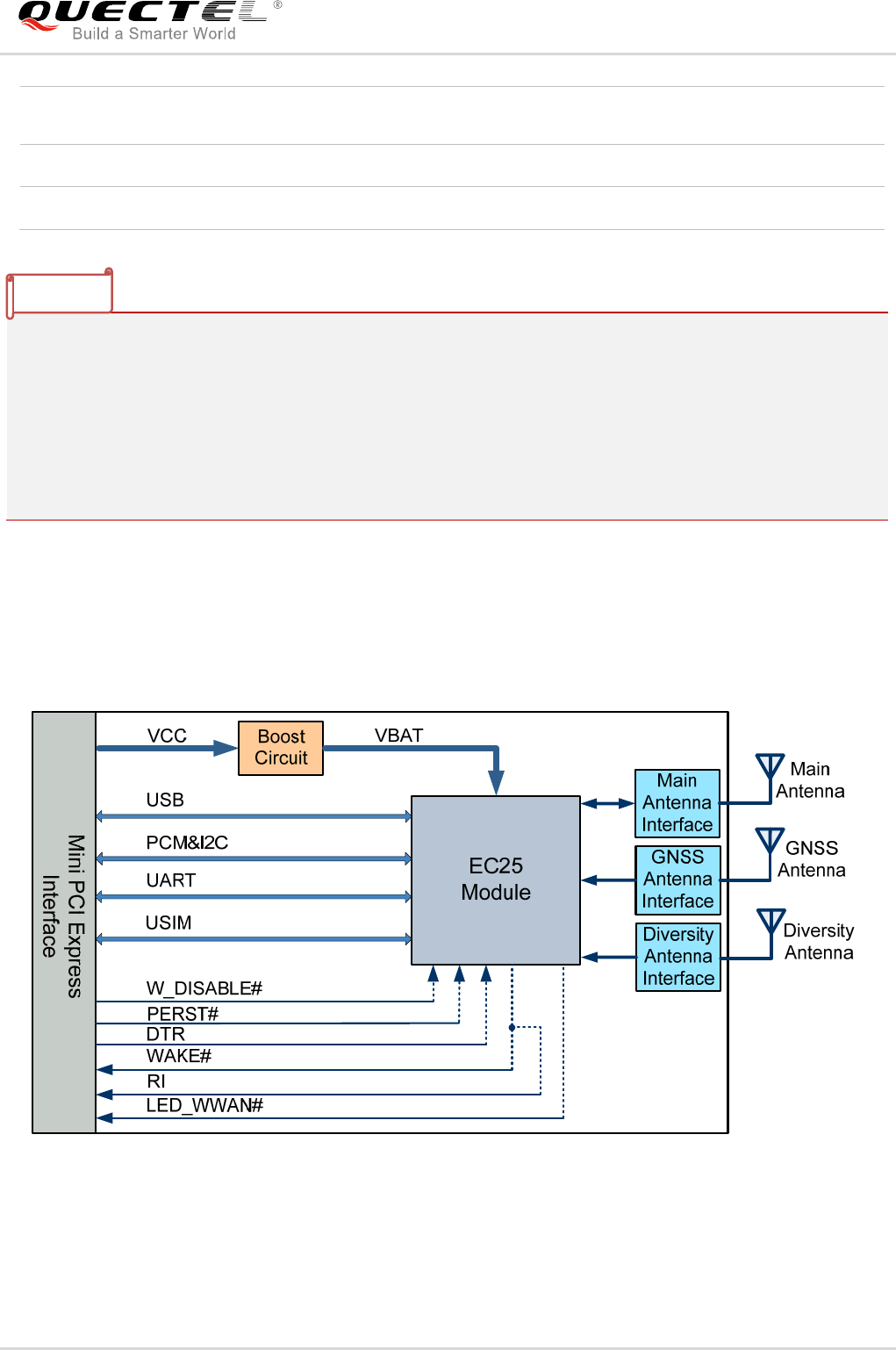
LTE Module Series
EC25 Mini PCIe Hardware Design
EC25_Mini_PCIe_Hardware_Design Confidential / Released 15 / 42
1. “*” means under development.
2. 1) Within operating temperature range, the module is 3GPP compliant.
3. 2) Within extended temperature range, the module remains the ability to establish and maintain a
voice, SMS, data transmission, emergency call, etc. There is no unrecoverable malfunction; there are
also no effects on radio spectrum and no harm to radio network. Only one or more parameters like
Pout might reduce in their value and exceed the specified tolerances. When the temperature returns
to normal operating temperature levels, the module is compliant with 3GPP specification again.
2.4. Functional Diagram
The following figure shows the block diagram of EC25 Mini PCIe.
Figure 1: Functional Diagram
Temperature Range Operation temperature range: -35°C ~ +75°C1)
Extended temperature range: -40°C ~ +80°C2)
Firmware Upgrade USB interface and DFOTA*
RoHS All hardware components are fully compliant with EU RoHS directive
NOTES

LTE Module Series
EC25 Mini PCIe Hardware Design
EC25_Mini_PCIe_Hardware_Design Confidential / Released 16 / 42
3 Application Interface
3.1. General Description
The physical connections and signal levels of EC25 Mini PCIe comply with PCI Express Mini CEM
specifications. This chapter mainly describes the following interfaces’ definition and application of EC25
Mini PCIe:
Power supply
USIM card interface
USB interface
UART interface
PCM&I2C interfaces
Control signals
Antenna interface
3.2. EC25 Mini PCIe Interface
3.2.1. Definition of Interface
The following tables show the pin definition and description of EC25 Mini PCIe on the 52-pin application.
Table 3: Definition of I/O Parameters
Type Description
IO Bidirectional
DI Digital input
DO Digital output
OC Open collector
PI Power input
PO Power output
LTE Module Series
EC25 Mini PCIe Hardware Design
EC25_Mini_PCIe_Hardware_Design Confidential / Released 17 / 42
Table 4: Description of Pins
Pin No. Mini PCI Express
Standard Name
EC25 Mini PCIe
Pin Name I/O Description Comment
1 WAKE# WAKE# OC
Output signal can be used
to wake up the host.
2 3.3Vaux VCC_3V3 PI 3.3V DC supply
3 COEX1 RESERVED Reserved
4 GND GND Mini card ground
5 COEX2 RESERVED Reserved
6 1.5V NC
7 CLKREQ# RESERVED Reserved
8 UIM_PWR USIM_VDD PO
Power source for the USIM
card
9 GND GND Mini card ground
10 UIM_DATA USIM_DATA IO USIM data signal
11 REFCLK- UART_RX DI UART receive data Connect to
DTE’s TX
12 UIM_CLK USIM_CLK DO USIM clock signal
13 REFCLK+ UART_TX DO UART transmit data Connect to
DTE’s RX
14 UIM_RESET USIM_RST DO USIM reset signal
15 GND GND Mini card ground
16 UIM_VPP RESERVED Reserved
17 RESERVED RI DO
Output signal can be used
to wake up the host.
18 GND GND Mini card ground
19 RESERVED RESERVED Reserved
20 W_DISABLE# W_DISABLE# DI
Disable wireless
communications
Pull-up by
default
Active low
21 GND GND Mini card ground
22 PERST# PERST# DI Functional reset to the card Active low
23 PERn0 UART_CTS DI UART clear to send Connect to
DTE’s RTS

LTE Module Series
EC25 Mini PCIe Hardware Design
EC25_Mini_PCIe_Hardware_Design Confidential / Released 18 / 42
24 3.3Vaux RESERVED Reserved
25 PERp0 UART_RTS DO UART request to send Connect to
DTE’s CTS
26 GND GND Mini card ground
27 GND GND Mini card ground
28 1.5V NC
29 GND GND Mini card ground
30 SMB_CLK I2C_SCL DO I2C serial clock
Require
external
pull-up to
1.8V.
31 PETn0 DTR DI Sleep mode control
32 SMB_DATA I2C_SDA IO I2C serial data
Require
external
pull-up to
1.8V.
33 PETp0 RESERVED Reserved
34 GND GND Mini card ground
35 GND GND Mini card ground
36 USB_D- USB_DM IO USB differential data (-)
37 GND GND Mini card ground
38 USB_D+ USB_DP IO USB differential data (+)
39 3.3Vaux VCC_3V3 PI 3.3V DC supply
40 GND GND Mini card ground
41 3.3Vaux VCC_3V3 PI 3.3V DC supply
42 LED_WWAN# LED_WWAN# OC
Active-low. LED signal for
indicating the state of the
card.
43 GND GND Mini card ground
44 LED_WLAN# RESERVED Reserved
45 RESERVED PCM_CLK* IO PCM clock signal
46 LED_WPAN# RESERVED Reserved
47 RESERVED PCM_DOUT* DO PCM data output
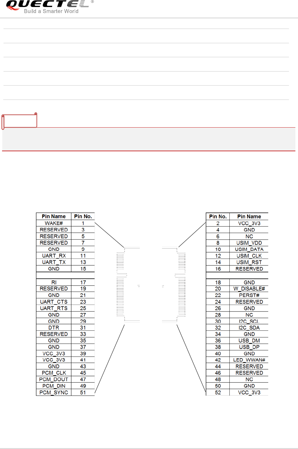
LTE Module Series
EC25 Mini PCIe Hardware Design
EC25_Mini_PCIe_Hardware_Design Confidential / Released 19 / 42
1. Keep all NC, reserved and unused pins unconnected.
2. “*” means the digital audio (PCM) function is only supported on Telematics version.
3.2.2. Pin Assignment
The following figure shows the pin assignment of EC25 Mini PCIe module. The top side contains EC25
module and antenna connectors.
PIN2
PIN52
BOT
PIN1
PIN51
TOP
Figure 2: Pin Assignment
48 1.5V NC
49 RESERVED PCM_DIN* DI PCM data input
50 GND GND Mini card ground
51 RESERVED PCM_SYNC* IO PCM frame synchronization
52 3.3Vaux VCC_3V3 PI 3.3V DC supply
NOTES
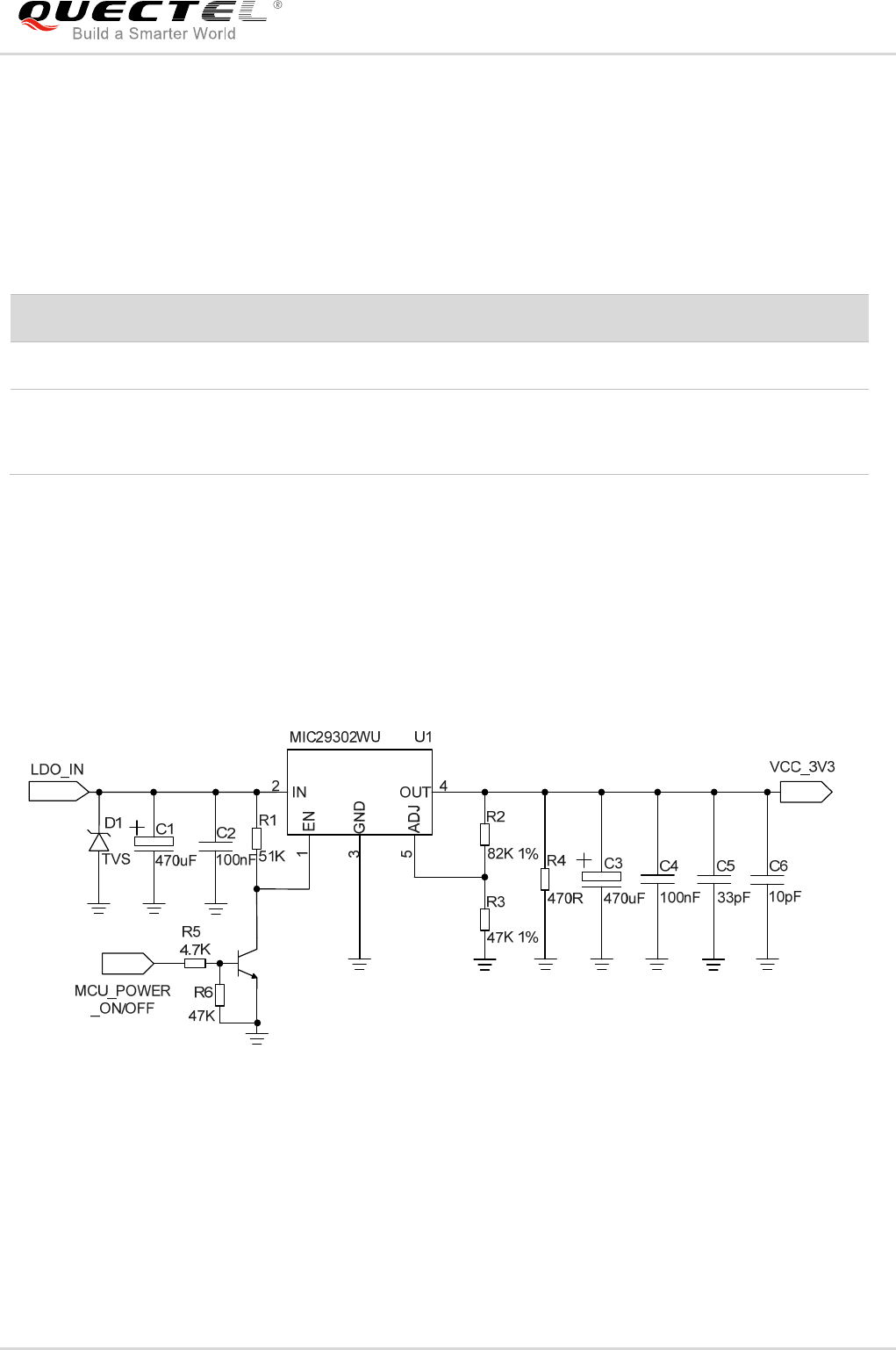
LTE Module Series
EC25 Mini PCIe Hardware Design
EC25_Mini_PCIe_Hardware_Design Confidential / Released 20 / 42
3.3. Power Supply
The following table shows pin definition of VCC_3V3 pins and ground pins.
Table 5: Definition of VCC_3V3 and GND Pins
The typical supply voltage of EC25 Mini PCIe is 3.3V. In the 2G networks, the input peak current may
reach to 2.7A during the transmitting time. Therefore, the power supply must be able to provide enough
current, and a bypass capacitor of no less than 470µF with low ESR should be used to prevent the
voltage from dropping.
The following figure shows a reference design of power supply. The precision of resistor R2 and R3 is 1%,
and the capacitor C3 needs a low ESR.
Figure 3: Reference Design of Power Supply
Pin No. Pin Name I/O Power Domain Description
2, 39, 41, 52 VCC_3V3 PI 3.0~3.6V 3.3V DC supply
4, 9, 15, 18, 21,
26, 27, 29, 34, 35,
37, 40, 43, 50
GND Mini card ground
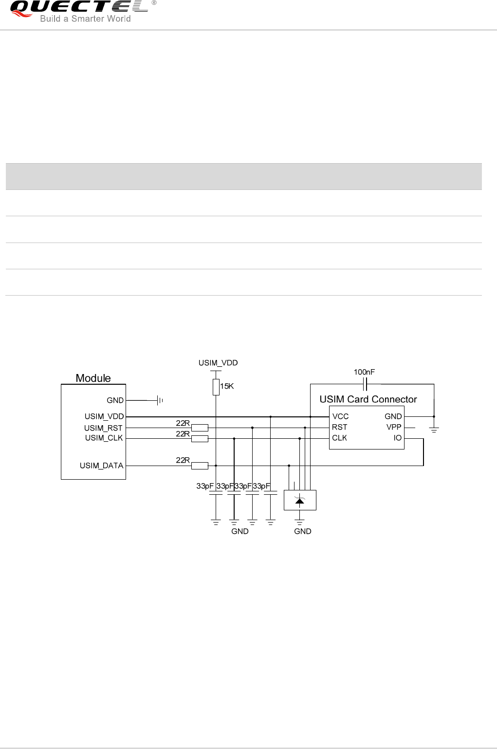
LTE Module Series
EC25 Mini PCIe Hardware Design
EC25_Mini_PCIe_Hardware_Design Confidential / Released 21 / 42
3.4. USIM Card Interface
The following table shows the pin definition of USIM card interface.
Table 6: USIM Pin Definition
EC25 Mini PCIe supports 1.8V and 3.0V USIM cards. The following figure shows a reference design for a
6-pin USIM card connector.
Figure 4: Reference Circuit of USIM Card Interface with a 6-Pin USIM Card Connector
In order to enhance the reliability and availability of the USIM card in your application, please follow the
criteria below in USIM circuit design:
Keep layout of USIM card as close to the module as possible. Keep the trace length as less than
200mm as possible.
Keep USIM card signal away from RF and power supply traces.
Keep the trace width of ground and USIM_VDD no less than 0.5mm to maintain the same electric
potential. The decouple capacitor of USIM_VDD should be less than 1uF and must near to USIM
card connector.
Pin No. Pin Name I/O Power Domain Description
8 USIM_VDD PO 1.8V/3.0V Power source for the USIM card
10 USIM_DATA IO 1.8V/3.0V USIM data signal
12 USIM_CLK DO 1.8V/3.0V USIM clock signal
14 USIM_RST DO 1.8V/3.0V USIM reset signal
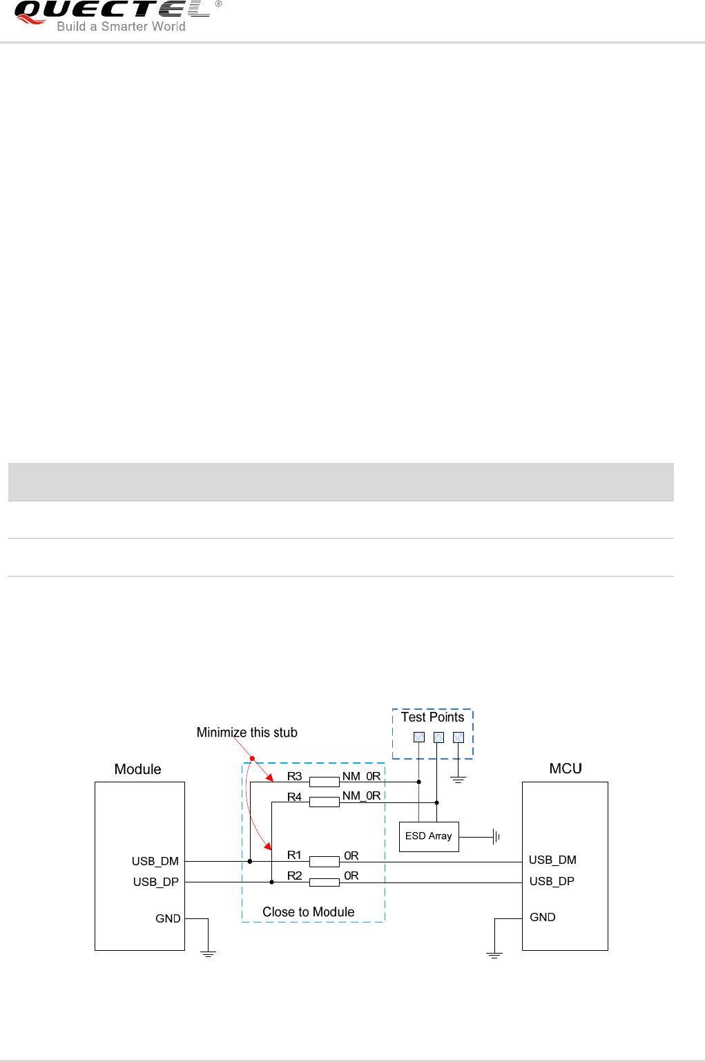
LTE Module Series
EC25 Mini PCIe Hardware Design
EC25_Mini_PCIe_Hardware_Design Confidential / Released 22 / 42
To avoid cross-talk between USIM_DATA and USIM_CLK, keep them away from each other and
shield them with surrounded ground.
In order to offer good ESD protection, it is recommended to add a TVS whose parasitic capacitance
should not be more than 50pF. The 22 ohm resistors should be added in series between the module
and the USIM card so as to suppress EMI spurious transmission and enhance ESD protection. The
33pF capacitors are used for filtering interference of GSM900. Please note that the USIM peripheral
circuit should be close to the USIM card connector.
The pull-up resistor on USIM_DATA line can improve anti-jamming capability when long layout trace
and sensitive occasion are applied, and should be placed close to the USIM card connector.
3.5. USB Interface
The following table shows the pin definition of USB interface.
Table 7: Pin Definition of USB Interface
EC25 Mini PCIe is compliant with USB 2.0 specification. It can only be used as a slave device. Meanwhile,
it supports high speed (480Mbps) mode and full speed (12Mbps) mode. The USB interface is used for AT
command communication, data transmission, GNSS NMEA output, software debugging, firmware
upgrade and voice over USB*. The following figure shows a reference circuit of USB interface.
Figure 5: Reference Circuit of USB Interface
Pin No. Pin Name I/O Description Comment
36 USB_DM IO USB differential data (-) Require differential impedance of 90Ω
38 USB_DP IO USB differential data (+) Require differential impedance of 90Ω
LTE Module Series
EC25 Mini PCIe Hardware Design
EC25_Mini_PCIe_Hardware_Design Confidential / Released 23 / 42
In order to ensure the integrity of USB data line signal, components R1, R2, R3 and R4 must be placed
close to the module, and also these resistors should be placed close to each other. The extra stubs of
trace must be as short as possible.
In order to ensure the USB interface design corresponding with the USB 2.0 specification, please comply
with the following principles:
It is important to route the USB signal traces as differential pairs with total grounding. The impedance
of USB differential trace is 90 ohm.
Do not route signal traces under crystals, oscillators, magnetic devices or RF signal traces. It is
important to route the USB differential traces in inner-layer with ground shielding on not only upper
and lower layers but also right and left sides.
If USB connector is used, please keep the ESD protection components to the USB connector as
close as possible. Pay attention to the influence of junction capacitance of ESD protection
components on USB data lines. Typically, the capacitance value should be less than 2pF.
Keep traces of USB data test points short to avoid noise coupled on USB data lines. If possible,
reserve a 0R resistor on these two lines.
1. There are three preconditions when enabling EC25 Mini PCIe to enter into the sleep mode:
a) Execute AT+QSCLK=1 command to enable the sleep mode. Please refer to document [2] for
details.
b) DTR pin should be kept in high level (pull-up internally).
c) USB interface on Mini PCIe must be connected with the USB interface of the host and please
guarantee the USB of the host is in suspended state.
2. “*” means under development.
3.6. UART Interface
The following table shows the pin definition of the UART interface.
Table 8: Pin Definition of the UART Interface
Pin No. EC25 Mini PCIe Pin Name I/O Power Domain Description
11 UART_RX DI 3.3V UART receive data
13 UART_TX DO 3.3V UART transmit data
23 UART_CTS DI 3.3V UART clear to send
25 UART_RTS DO 3.3V UART request to send
NOTES
LTE Module Series
EC25 Mini PCIe Hardware Design
EC25_Mini_PCIe_Hardware_Design Confidential / Released 24 / 42
The UART interface supports 9600, 19200, 38400, 57600, 115200 and 230400bps baud rate. The default
is 115200bps. This interface can be used for AT command communication.
AT+IPR command can be used to set the baud rate of the UART, and AT+IFC command can be used to
set the hardware flow control (hardware flow control is disabled by default). Please refer to document [2]
for details.
3.7. PCM and I2C Interfaces
The following table shows the pin definition of PCM and 12C interfaces that can be applied in audio codec
design.
Table 9: Pin Definition of PCM and I2C Interfaces
EC25 Mini PCIe provides one PCM digital interface, which supports 8-bit A-law* and μ-law*, and also
supports 16-bit linear data formats and the following modes:
Primary mode (short frame synchronization, works as either master or slave)
Auxiliary mode (long frame synchronization, works as master only)
“*” means under development.
Pin No. Pin Name I/O Power Domain Description
45 PCM_CLK IO 1.8V PCM clock signal
47 PCM_DOUT DO 1.8V PCM data output
49 PCM_DIN DI 1.8V PCM data input
51 PCM_SYNC IO 1.8V PCM frame synchronization
30 I2C_SCL DO 1.8V I2C serial clock, require external
pull-up to 1.8V.
32 I2C_SDA IO 1.8V I2C serial data, require external
pull-up to 1.8V.
NOTE
NOTE
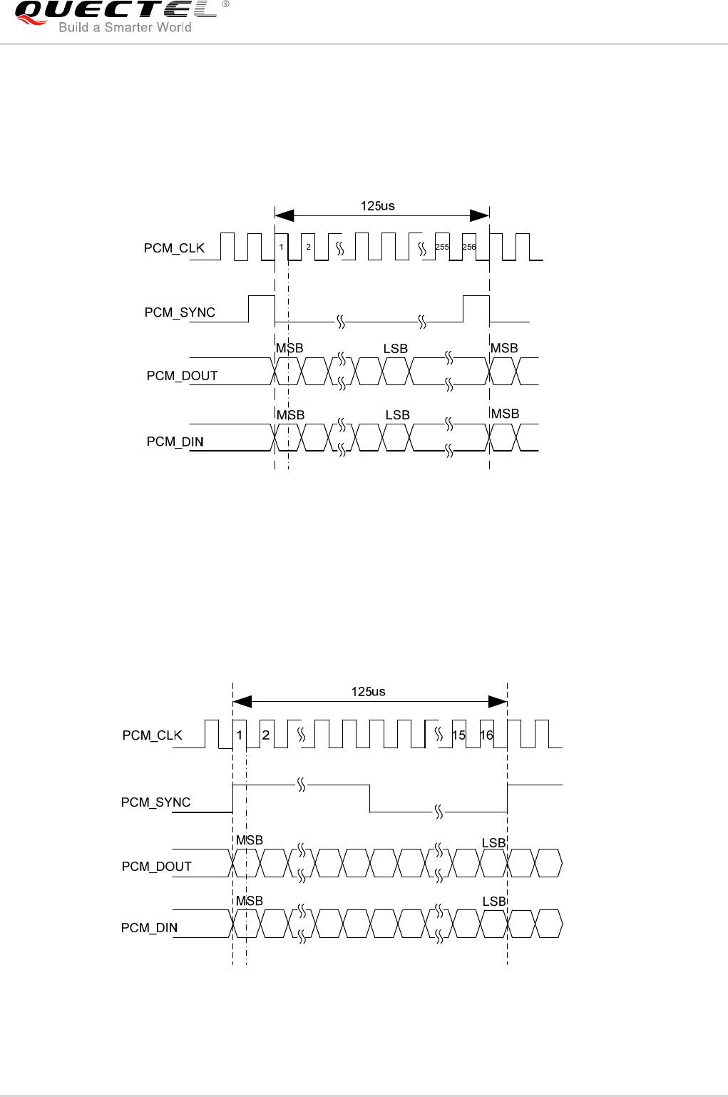
LTE Module Series
EC25 Mini PCIe Hardware Design
EC25_Mini_PCIe_Hardware_Design Confidential / Released 25 / 42
In primary mode, the data is sampled on the falling edge of the PCM_CLK and transmitted on the rising
edge. The PCM_SYNC falling edge represents the MSB. In this mode, PCM_CLK supports 128, 256, 512,
1024 and 2048kHz for different speed codecs. The following figure shows the timing relationship in
primary mode with 8kHz PCM_SYNC and 2048kHz PCM_CLK.
Figure 6: Timing in Primary Mode
In auxiliary mode, the data is sampled on the falling edge of the PCM_CLK and transmitted on the rising
edge; while the PCM_SYNC rising edge represents the MSB. In this mode, PCM interface operates with a
128kHz PCM_CLK and an 8kHz, 50% duty cycle PCM_SYNC only. The following figure shows the timing
relationship in auxiliary mode with 8kHz PCM_SYNC and 128kHz PCM_CLK.
Figure 7: Timing in Auxiliary Mode
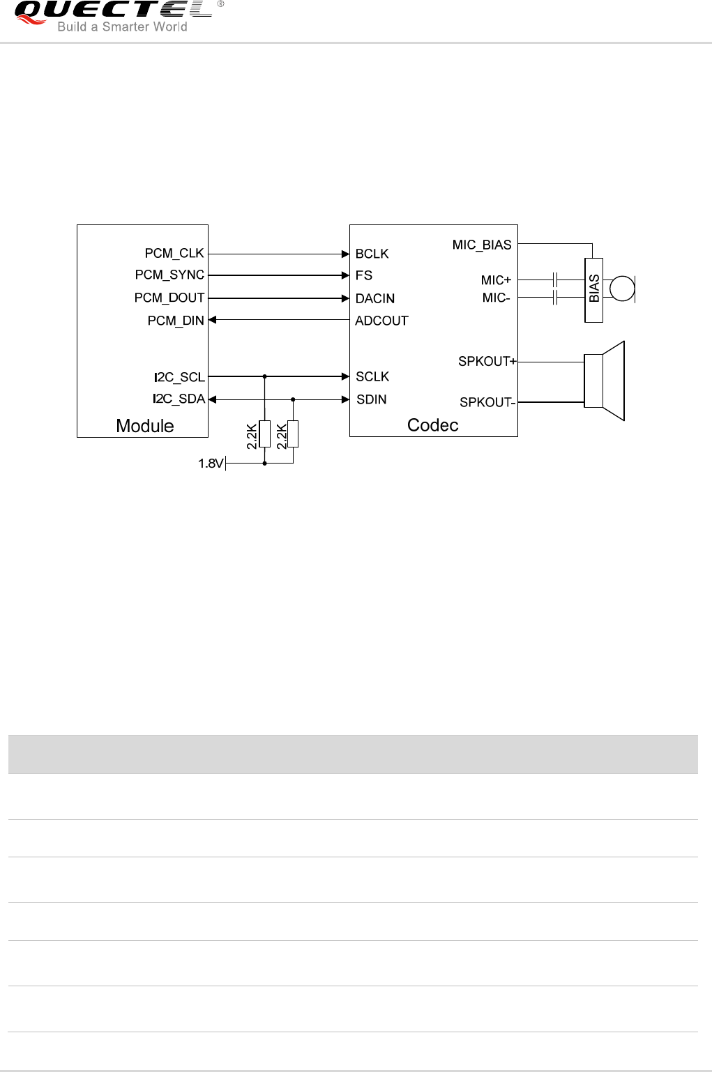
LTE Module Series
EC25 Mini PCIe Hardware Design
EC25_Mini_PCIe_Hardware_Design Confidential / Released 26 / 42
Clock and mode can be configured by AT command, and the default configuration is master mode using
short frame synchronization format with 2048kHz PCM_CLK and 8kHz PCM_SYNC. In addition, EC25
Mini PCIe’s firmware has integrated the configuration on some PCM codec’s application with I2C interface.
Please refer to document [2] for details about AT+QDAI command.
The following figure shows a reference design of PCM interface with an external codec IC.
Figure 8: Reference Circuit of PCM Application with Audio Codec
3.8. Control Signals
The following table shows the pin definition of control signals.
Table 10: Pin Definition of Control Signals
Pin No. Pin Name I/O Power Domain Description
17 RI DO 3.3V Output signal can be used to wake up
the host.
31 DTR DI 3.3V Sleep mode control
20 W_DISABLE# DI 3.3V Disable wireless communications;
pull-up by default, active low.
22 PERST# DI 3.3V Functional reset to the card; active low.
42 LED_WWAN# OC Active-low. LED signal for indicating the
state of the module.
1 WAKE# OC
Output signal can be used to wake up
the host.
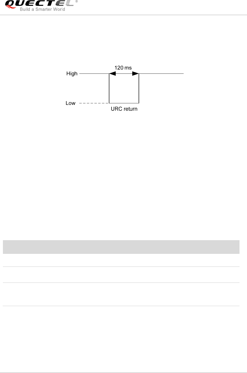
LTE Module Series
EC25 Mini PCIe Hardware Design
EC25_Mini_PCIe_Hardware_Design Confidential / Released 27 / 42
3.8.1. RI Signal
The RI signal can be used to wake up the host. When URC returns, there will be the following behavior on
the RI pin after executing AT+QCFG=“risignaltype”,“physical” command.
Figure 9: RI Behavior
3.8.2. DTR Signal
The DTR signal supports sleep control function. Driving it to low level will wake up the module.
3.8.3. W_DISABLE# Signal
EC25 Mini PCIe provides W_DISABLE# signal to disable wireless communications through hardware
operation. The following table shows the radio operational states of the module. Please refer to
document [2] for related AT commands.
Table 11: Radio Operational States
3.8.4. PERST# Signal
The PERST# signal can be used to force a hardware reset on the card. You can reset the module by
driving the PERST# to a low level voltage with the time frame of 150~460ms and then releasing it. The
reset scenario is illustrated in the following figure.
W_DISABLE# AT Commands Radio Operation
High Level AT+CFUN=1 Enabled
High Level AT+CFUN=0
AT+CFUN=4 Disabled
Low Level
AT+CFUN=0
AT+CFUN=1
AT+CFUN=4
Disabled
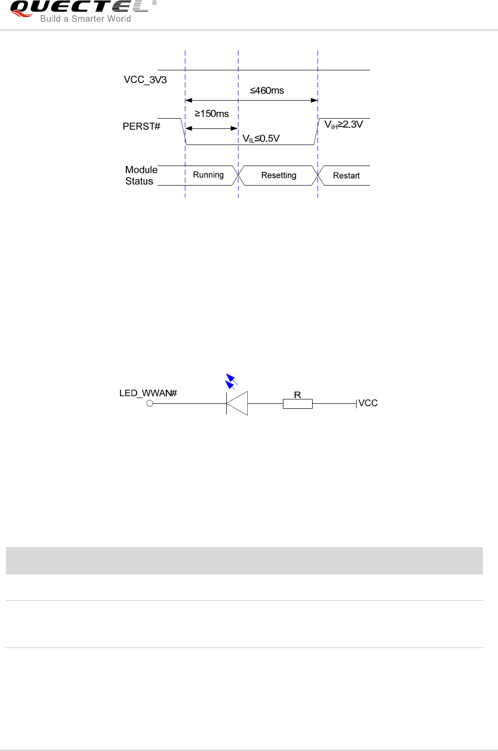
LTE Module Series
EC25 Mini PCIe Hardware Design
EC25_Mini_PCIe_Hardware_Design Confidential / Released 28 / 42
Figure 10: Timing of Resetting Module
3.8.5. LED_WWAN# Signal
The LED_WWAN# signal of EC25 Mini PCIe is used to indicate the network status of the module, which
can absorb the current up to 40mA. According to the following circuit, in order to reduce the current of the
LED, a resistor must be placed in series with the LED. The LED is emitting light when the LED_WWAN#
output signal is active low.
Figure 11: LED_WWAN# Signal Reference Circuit Diagram
The following table shows the network status indications of the LED_WWAN# signal.
Table 12: Indications of Network Status
LED_WWAN# Description
Low Level (Light on) Registered on network
High-impedance (Light off)
No network coverage or not registered
W_DISABLE# signal is at low level. (Disable the RF)
AT+CFUN=0, AT+CFUN=4
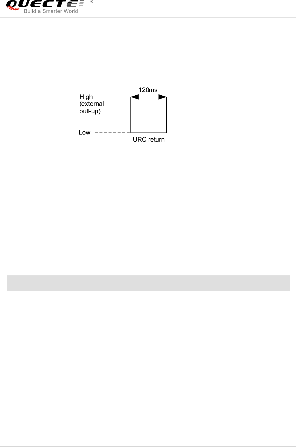
LTE Module Series
EC25 Mini PCIe Hardware Design
EC25_Mini_PCIe_Hardware_Design Confidential / Released 29 / 42
3.8.6. WAKE# Signal
The WAKE# signal is an open collector signal which is similar to RI signal, but a host pull-up resistor and
AT+QCFG=“risignaltype”,“physical” command are required. When URC returns, there will be 120ms
low level pulse output as below.
Figure 12: WAKE# Behavior
3.9. Antenna Interfaces
EC25 Mini PCIe antenna interfaces include a main antenna interface, an Rx-diversity antenna interface
and a GNSS antenna interface. And Rx-diversity function is enabled by default.
The following table shows the requirement on main antenna, Rx-diversity antenna and GNSS antenna.
Table 13: Antenna Requirements
Type Requirements
GNSS
Frequency range: 1561~1615MHz
Polarization: RHCP or linear
VSWR: <2 (Typ.)
Passive antenna gain: >0dBi
GSM/WCDMA/LTE
VSWR: ≤2
Gain (dBi): 1
Max Input Power (W): 50
Input Impedance (ohm): 50
Polarization Type: Vertical
Cable Insertion Loss: <1dB
(GSM900, WCDMA B5/B8, LTE B5/B8/B12/B17/B20)
Cable Insertion Loss: <1.5dB
(GSM1800, WCDMA B1/B2/B3/B4, LTE B1/B2/B3/B4)
Cable insertion loss: <2dB
(LTE B7/B38/B40/B41)
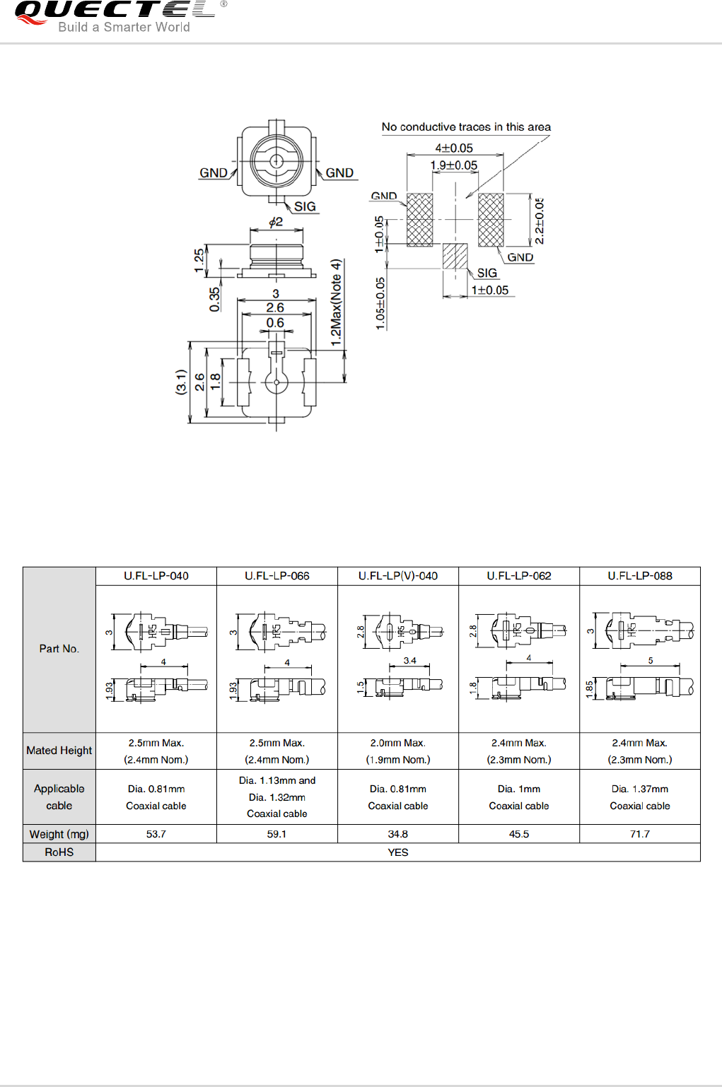
LTE Module Series
EC25 Mini PCIe Hardware Design
EC25_Mini_PCIe_Hardware_Design Confidential / Released 30 / 42
The following figure shows the overall sizes of RF connector.
Figure 13: Dimensions of the RF Connector (Unit: mm)
U.FL-LP serial connectors listed in the following figure can be used to match the RF connector.
Figure 14: Mechanicals of U.FL-LP Connectors

LTE Module Series
EC25 Mini PCIe Hardware Design
EC25_Mini_PCIe_Hardware_Design Confidential / Released 31 / 42
4 Electrical and Radio Characteristics
4.1. General Description
This chapter mainly describes the following electrical and radio characteristics of EC25 Mini PCIe:
Power supply requirements
I/O requirements
Current consumption
RF characteristics
GNSS receiver
ESD characteristics
4.2. Power Supply Requirements
The input voltage of EC25 Mini PCIe is 3.3V±9%, as specified by PCI Express Mini CEM Specifications
1.2. The following table shows the power supply requirements of EC25 Mini PCIe.
Table 14: Power Supply Requirements
Parameter Description Min. Typ. Max. Unit
VCC_3V3 Power Supply 3.0 3.3 3.6 V
LTE Module Series
EC25 Mini PCIe Hardware Design
EC25_Mini_PCIe_Hardware_Design Confidential / Released 32 / 42
4.3. I/O Requirements
The following table shows the I/O requirements of EC25 Mini PCIe.
Table 15: I/O Requirements
1. The PCM and I2C interfaces belong to 1.8V power domain and other I/O interfaces belong to
VCC_3V3 power domain.
2. The maximum voltage value of VIL for PERST# signal and W_DISABLE# signal is 0.5V.
4.4. RF Characteristics
The following tables show the conducted RF output power and receiving sensitivity of EC25 Mini PCIe
module.
Table 16: EC25 Mini PCIe Conducted RF Output Power
Parameter Description Min. Max. Unit
VIH Input High Voltage 0.7 × VCC_3V3 VCC_3V3+0.3 V
VIL Input Low Voltage -0.3 0.3 × VCC_3V3 V
VOH Output High Voltage VCC_3V3-0.5 VCC_3V3 V
VOL Output Low Voltage 0 0.4 V
Frequency Max. Min.
GSM850/GSM900 33dBm±2dB 5dBm±5dB
DCS1800/PCS1900 30dBm±2dB 0dBm±5dB
GSM850/GSM900 (8-PSK) 27dBm±3dB 5dBm±5dB
DCS1800/PCS1900 (8-PSK) 26dBm±3dB 0dBm±5dB
WCDMA bands 24dBm+1/-3dB <-50dBm
LTE-FDD bands 23dBm±2dB <-44dBm
NOTES
LTE Module Series
EC25 Mini PCIe Hardware Design
EC25_Mini_PCIe_Hardware_Design Confidential / Released 33 / 42
Table 17: EC25-A Mini PCIe Conducted RF Receiving Sensitivity
Table 18: EC25-J Mini PCIe Conducted RF Receiving Sensitivity
LTE-TDD bands 23dBm±2dB <-44dBm
Frequency Primary Diversity SIMO 3GPP (SIMO)
WCDMA B2 -110.0dBm / / -104.7dBm
WCDMA B4 -110.0dBm / / -106.7dBm
WCDMA B5 -110.5dBm / / -104.7dBm
LTE FDD B2 (10M) -98.0dBm -98.0dBm -101.0dBm -94.3dBm
LTE FDD B4 (10M) -97.5dBm -99.0dBm -101.0dBm -96.3dBm
LTE FDD B12 (10M) -96.5dBm -98.0dBm -101.0dBm -93.3dBm
Frequency Primary Diversity SIMO 3GPP (SIMO)
WCDMA B1 -110.0dBm / / -106.7dBm
WCDMA B6 -110.5dBm / / -106.7dBm
WCDMA B8 -110.5dBm / / -106.7dBm
WCDMA B19 -110.5dBm / / -106.7dBm
LTE-FDD B1 (10M) -97.5dBm -98.7dBm -100.2dBm -96.3dBm
LTE-FDD B3 (10M) -96.5dBm -97.1dBm -100.5dBm -93.3dBm
LTE-FDD B8 (10M) -98.4dBm -99.0dBm -101.2dBm -93.3dBm
LTE-FDD B18 (10M) -99.5dBm -99.0dBm -101.7dBm -96.3dBm
LTE-FDD B19 (10M) -99.2dBm -99.0dBm -101.4dBm -96.3dBm
LTE-FDD B26 (10M) -99.5dBm -99.0dBm -101.5dBm -93.8dBm
LTE-TDD B41 (10M) -95.0dBm -95.7dBm -99.0dBm -94.3dBm
LTE Module Series
EC25 Mini PCIe Hardware Design
EC25_Mini_PCIe_Hardware_Design Confidential / Released 34 / 42
Table 19: EC25-E Mini PCIe Conducted RF Receiving Sensitivity
Table 20: EC25-V Mini PCIe Conducted RF Receiving Sensitivity
4.5. GNSS Receiver
EC25 Mini PCIe integrates a GNSS receiver that supports IZat Gen 8C Lite of Qualcomm (GPS,
GLONASS, BeiDou, Galileo, QZSS). Meanwhile, it supports Qualcomm gpsOneXTRA technology (one
kind of A-GNSS). This technology will download XTRA file from the internet server to enhance the TTFF.
Frequency Primary Diversity SIMO 3GPP (SIMO)
GSM900 -109.0dBm / / -102.0dBm
DCS1800 -109.0dBm / / -102.0dbm
WCDMA B1 -110.5dBm / / -106.7dBm
WCDMA B5 -110.5dBm / / -104.7dBm
WCDMA B8 -110.5dBm / / -103.7dBm
LTE-FDD B1 (10M) -98.0dBm -98.0dBm -101.5dBm -96.3dBm
LTE-FDD B3 (10M) -96.5dBm -98.5dBm -101.5dBm -93.3dBm
LTE-FDD B5 (10M) -98.0dBm -98.5dBm -101.0dBm -94.3dBm
LTE-FDD B7 (10M) -97.0dBm -94.5dBm -99.5dBm -94.3dBm
LTE-FDD B8 (10M) -97.0dBm -97.0dBm -101.0dBm -93.3dBm
LTE-FDD B20 (10M) -97.5dBm -99.0dBm -102.5dBm -93.3dBm
LTE-TDD B38 (10M) -96.7dBm -97.0dBm -100.0dBm -96.3dBm
LTE-TDD B40 (10M) -96.3dBm -98.0dBm -101.0dBm -96.3dBm
LTE-TDD B41 (10M) -95.2dBm -95.7dBm -99.0dBm -94.3dBm
Frequency Primary Diversity SIMO 3GPP (SIMO)
LTE-FDD B4 (10M) -97.5dBm -99.0dBm -101.0dBm -96.3dBm
LTE-FDD B13 (10M) -95.0dBm -97.0dBm -100.0dBm -93.3dBm
LTE Module Series
EC25 Mini PCIe Hardware Design
EC25_Mini_PCIe_Hardware_Design Confidential / Released 35 / 42
XTRA file contains predicted GPS and GLONASS satellites coordinates and clock biases valid for up to 7
days. It is best if XTRA file is downloaded every 1-2 days. Additionally, EC25 Mini PCIe can support
standard NMEA-0183 protocol and output NMEA messages with 1Hz via USB NMEA interface.
EC25 Mini PCIe GNSS engine is switched off by default. You must switch on it by AT command. Please
refer to document [3] for more details about GNSS engine technology and configurations. A passive
antenna should be used for the GNSS engine.
4.6. ESD Characteristics
The following table shows the ESD characteristics of EC25 Mini PCIe.
Table 21: ESD Characteristics of EC25 Mini PCIe
4.7. Current Consumption
The following tables describe the current consumption of EC25 Mini PCIe series module.
Table 22: Current Consumption of EC25-A Mini PCIe
Parameter Description Conditions Typ. Unit
IVBAT Sleep state
AT+CFUN=0 (USB disconnected) 3.6 mA
WCDMA PF=64 (USB disconnected) 4.4 mA
WCDMA PF=128 (USB disconnected) 3.8 mA
LTE-FDD PF=64 (USB disconnected) 5.9 mA
Part Contact Discharge Air Discharge Unit
Power Supply and GND +/-5 +/-10 kV
Antenna Interface +/-4 +/-8 kV
USB Interface +/-4 +/-8 kV
USIM Interface +/-4 +/-8 kV
Others +/-0.5 +/-1 kV
LTE Module Series
EC25 Mini PCIe Hardware Design
EC25_Mini_PCIe_Hardware_Design Confidential / Released 36 / 42
LTE-FDD PF=128 (USB disconnected) 4.8 mA
Idle state
WCDMA PF=64 (USB disconnected) 27.0 mA
WCDMA PF=64 (USB connected) 40.0 mA
LTE-FDD PF=64 (USB disconnected) 43.0 mA
LTE-FDD PF=64 (USB connected) 59.0 mA
WCDMA data
transfer
(GNSS OFF)
WCDMA B2 HSDPA @22.63dBm 764.0 mA
WCDMA B2 HSUPA @23.19dBm 741.0 mA
WCDMA B4 HSDPA @22.45dBm 745.0 mA
WCDMA B4 HSUPA @22.57dBm 752.0 mA
WCDMA B5 HSDPA @22.49dBm 616.0 mA
WCDMA B5 HSUPA @22.43dBm 637.0 mA
LTE data
transfer
(GNSS OFF)
LTE-FDD B2 @22.92dBm 977.0 mA
LTE-FDD B4 @23.42dBm 1094.0 mA
LTE-FDD B12 @23.39dBm 847.0 mA
WCDMA
voice call
WCDMA B2 @23.59dBm 861.0 mA
WCDMA B4 @23.47dBm 812.0 mA
WCDMA B5 @23.46dBm 683.0 mA
Table 23: Current Consumption of EC25-E Mini PCIe
Parameter Description Conditions Typ. Unit
IVBAT Sleep state
AT+CFUN=0 (USB disconnected) 3.9 mA
GSM DRX=2 (USB disconnected) 5.1 mA
GSM DRX=9 (USB disconnected) 4.3 mA
WCDMA PF=64 (USB disconnected) 5.5 mA
WCDMA PF=128 (USB disconnected) 4.8 mA
LTE-FDD PF=64 (USB disconnected) 5.8 mA

LTE Module Series
EC25 Mini PCIe Hardware Design
EC25_Mini_PCIe_Hardware_Design Confidential / Released 37 / 42
LTE-FDD PF=128 (USB disconnected) 5.0 mA
LTE-TDD PF=64 (USB disconnected) 5.8 mA
LTE-TDD PF=128 (USB disconnected) 4.9 mA
Idle state
GSM DRX=5 (USB disconnected) 30.0 mA
GSM DRX=5 (USB connected) 43.0 mA
WCDMA PF=64 (USB disconnected) 31.0 mA
WCDMA PF=64 (USB connected) 45.0 mA
LTE-FDD PF=64 (USB disconnected) 31.0 mA
LTE-FDD PF=64 (USB connected) 44.0 mA
LTE-TDD PF=64 (USB disconnected) 32.0 mA
LTE-TDD PF=64 (USB connected) 44.0 mA
GPRS data
transfer
(GNSS OFF)
GSM900 4DL/1UL @33.08dBm 372.0 mA
GSM900 3DL/2UL @31.03dBm 626.0 mA
GSM900 2DL/3UL @29.86dBm 706.0 mA
GSM900 1DL/4UL @29.44dBm 767.0 mA
DCS1800 4DL/1UL @30.39dBm 262.0 mA
DCS1800 3DL/2UL @30.19dBm 417.0 mA
DCS1800 2DL/3UL @30.02dBm 564.0 mA
DCS1800 1DL/4UL @29.86dBm 709.0 mA
EDGE data
transfer
(GNSS OFF)
GSM900 4DL/1UL @27.59dBm 233.0 mA
GSM900 3DL/2UL @27.45dBm 370.0 mA
GSM900 2DL/3UL @27.31dBm 500.0 mA
GSM900 1DL/4UL @27.14dBm 623.0 mA
DCS1800 4DL/1UL @26.24dBm 224.0 mA
DCS1800 3DL/2UL @26.13dBm 334.0 mA
LTE Module Series
EC25 Mini PCIe Hardware Design
EC25_Mini_PCIe_Hardware_Design Confidential / Released 38 / 42
DCS1800 2DL/3UL @25.97dBm 440.0 mA
DCS1800 1DL/4UL @25.82dBm 553.0 mA
WCDMA data
transfer
(GNSS OFF)
WCDMA B1 HSDPA @22.49dBm 798.0 mA
WCDMA B1 HSUPA @21.87dBm 788.0 mA
WCDMA B5 HSDPA @22.66dBm 781.0 mA
WCDMA B5 HSUPA @21.99dBm 770.0 mA
WCDMA B8 HSDPA @22.23dBm 655.0 mA
WCDMA B8 HSUPA @21.68dBm 659.0 mA
LTE data
transfer
(GNSS OFF)
LTE-FDD B1 @23.12dBm 940.0 mA
LTE-FDD B3 @22.75dBm 989.0 mA
LTE-FDD B5 @22.92dBm 962.0 mA
LTE-FDD B7 @23.42dBm 1188.0 mA
LTE-FDD B8 @22.97dBm 911.0 mA
LTE-FDD B20 @22.51dBm 946.0 mA
LTE-TDD B38 @22.58dBm 686.0 mA
LTE-TDD B40 @22.31dBm 576.0 mA
LTE-TDD B41 @22.03dBm 611.0 mA
GSM
voice call
GSM900 PCL=5 @33.31dBm 367.0 mA
DCS1800 PCL=0 @20.48dBm 248.0 mA
WCDMA
voice call
WCDMA B1 @23.18dBm 868.0 mA
WCDMA B5 @22.62dBm 808.0 mA
WCDMA B8 @23.02dBm 728.0 mA
LTE Module Series
EC25 Mini PCIe Hardware Design
EC25_Mini_PCIe_Hardware_Design Confidential / Released 39 / 42
Table 24: Current Consumption of EC25-V Mini PCIe
Parameter Description Conditions Typ. Unit
IVBAT
Sleep state
AT+CFUN=0 (USB disconnected) 3.4 mA
LTE-FDD PF=64 (USB disconnected) 4.8 mA
LTE-FDD PF=128 (USB disconnected) 4.3 mA
Idle state
LTE-FDD PF=64 (USB disconnected) 30.0 mA
LTE-FDD PF=64 (USB connected) 42.0 mA
LTE data
transfer
(GNSS OFF)
LTE-FDD B4 @23.3dBm 873.0 mA
LTE-FDD B13 @22.13dBm 638.0 mA
Table 25: GNSS Current Consumption of EC25 Mini PCIe Series Module
Parameter Description Conditions Typ. Unit
IVBAT
(GNSS)
Searching
(AT+CFUN=0)
Cold start @Passive Antenna 75.0 mA
Lost state @Passive Antenna 74.0 mA
Tracking
(AT+CFUN=0)
Instrument environment 44.0 mA
Open Sky @Passive Antenna 53.0 mA
Open Sky @Active Antenna 58.0 mA
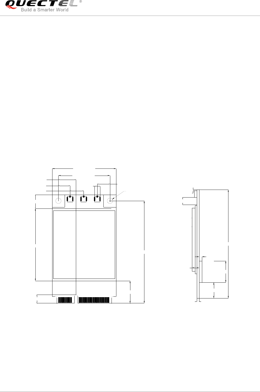
LTE Module Series
EC25 Mini PCIe Hardware Design
EC25_Mini_PCIe_Hardware_Design Confidential / Released 40 / 42
5 Dimensions and Packaging
5.1. General Description
This chapter mainly describes mechanical dimensions as well as packaging specification of EC25 Mini
PCIe module.
5.2. Mechanical Dimensions of EC25 Mini PCIe
10.35±0.10
34.30±0.20
4.00±0.10
48.05±0.20
6.35±0.10
3x3.00 5.98±0.10
6.38±0.10
5.45±0.10
8.25±0.10 24.20±0.20
30.00±0.20
Pin1 Pin51
Top View
1.00
7.26±0.10
1.40
4.90±0.20
0.61
2.35±0.10
50.95±0.20
9.90±0.10
Side View
2xΦ2.60
Figure 15: Mechanical Dimensions of EC25 Mini PCIe (Unit: mm)
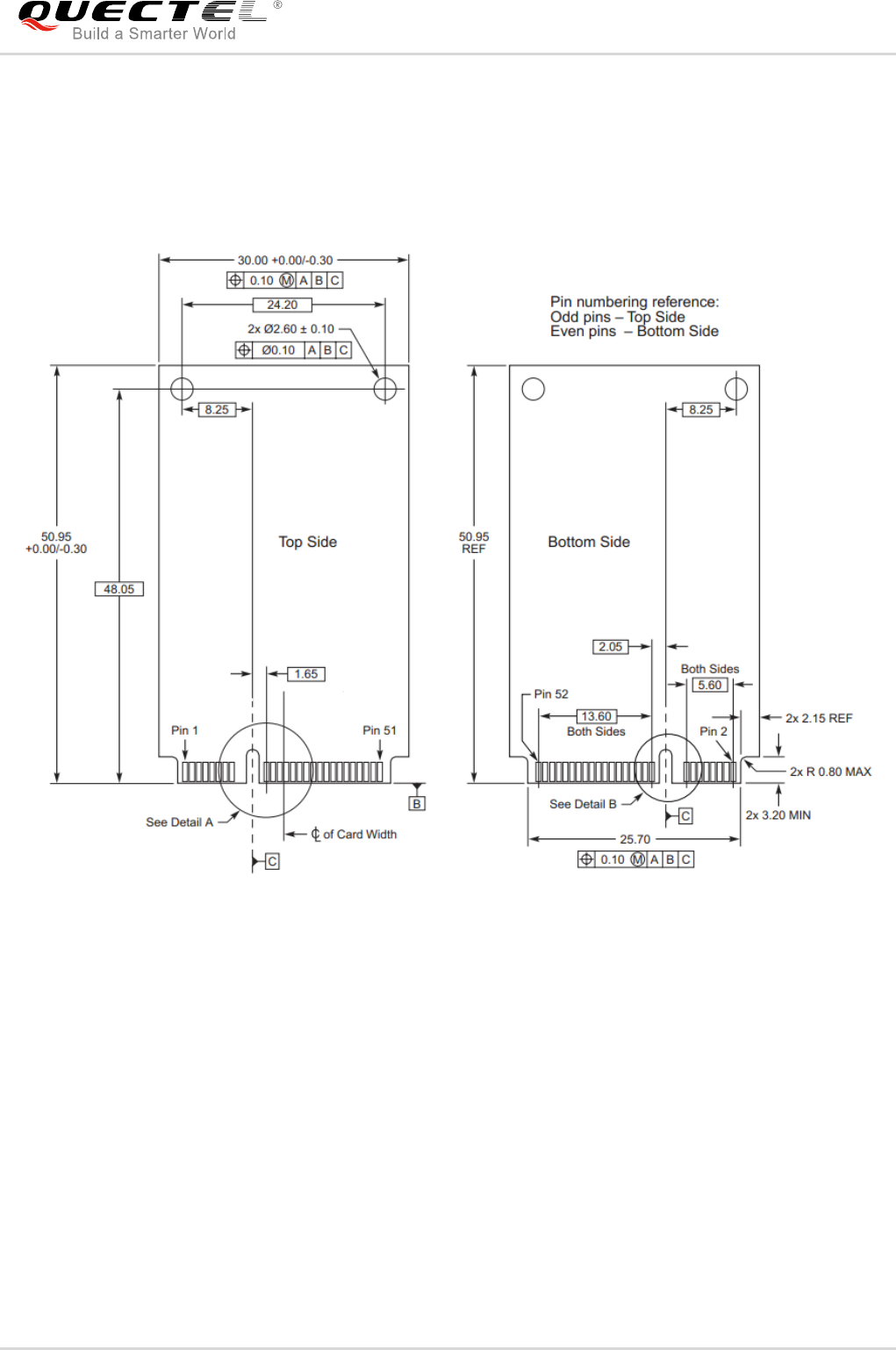
LTE Module Series
EC25 Mini PCIe Hardware Design
EC25_Mini_PCIe_Hardware_Design Confidential / Released 41 / 42
5.3. Standard Dimensions of Mini PCI Express
The following figure shows the standard dimensions of Mini PCI Express. Please refer to document [1]
for detailed A and B.
Figure 16: Standard Dimensions of Mini PCI Express (Unit: mm)
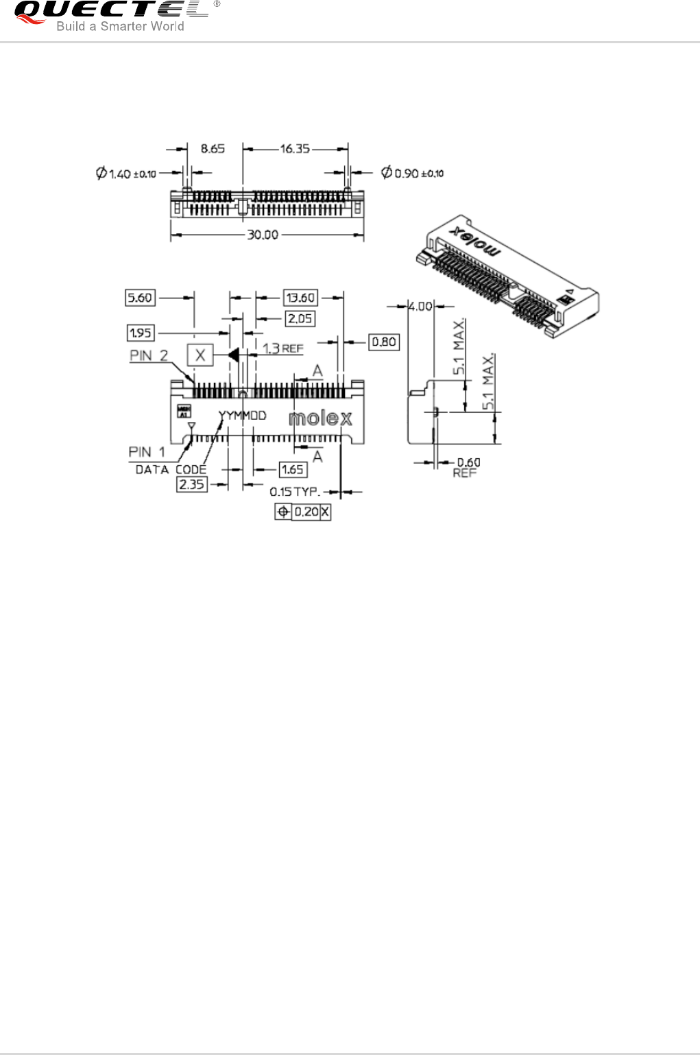
LTE Module Series
EC25 Mini PCIe Hardware Design
EC25_Mini_PCIe_Hardware_Design Confidential / Released 42 / 42
EC25 Mini PCIe adopts a standard Mini PCI Express connector which compiles with the directives and
standards listed in the document [1]. The following figure takes the Molex 679100002 as an example.
Figure 17: Dimensions of the Mini PCI Express Connector (Molex 679100002, Unit: mm)
5.4. Packaging Specification
The EC25 Mini PCIe is packaged in a tray. Each tray contains 10pcs of modules. The smallest package of
EC25 Mini PCIe contains 100pcs.
LTE Module Series
EC25 Mini PCIe Hardware Design
EC25_Mini_PCIe_Hardware_Design Confidential / Released 43 / 42
6 Appendix References
Table 26: Related Documents
Table 27: Terms and Abbreviations
SN Document Name Remark
[1] PCI Express Mini Card Electromechanical
Specification Revision 1.2 Mini PCI Express Specification
[2] Quectel_EC25&EC21_AT_Commands_Manual EC25 and EC21 AT Commands Manual
[3] Quectel_EC25&EC21_GNSS_AT_Commands_
Manual
EC25 and EC21 GNSS AT Commands
Manual
Abbreviation Description
AMR Adaptive Multi-rate
bps Bits Per Second
CS Coding Scheme
DC-HSPA+ Dual-carrier High Speed Packet Access
DFOTA Delta Firmware Upgrade Over The Air
DL Down Link
EFR Enhanced Full Rate
ESD Electrostatic Discharge
FDD Frequency Division Duplexing
FR Full Rate
GLONASS GLObalnaya Navigatsionnaya Sputnikovaya Sistema, the Russian Global
Navigation Satellite System
GMSK Gaussian Minimum Shift Keying

LTE Module Series
EC25 Mini PCIe Hardware Design
EC25_Mini_PCIe_Hardware_Design Confidential / Released 44 / 42
GNSS Global Navigation Satellite System
GPS Global Positioning System
GSM Global System for Mobile Communications
HR Half Rate
kbps Kilo Bits Per Second
LED Light Emitting Diode
LTE Long-Term Evolution
Mbps Million Bits Per Second
ME Mobile Equipment (Module)
MIMO Multiple-Input Multiple-Output
MMS Multimedia Messaging Service
MO Mobile Originated
MT Mobile Terminated
PCM Pulse Code Modulation
PDU Protocol Data Unit
PPP Point-to-Point Protocol
RF Radio Frequency
Rx Receive
USIM Universal Subscriber Identification Module
SIMO Single Input Multiple Output
SMS Short Message Service
UART Universal Asynchronous Receiver & Transmitter
UL Up Link
URC Unsolicited Result Code
WCDMA Wideband Code Division Multiple Access