Quectel Wireless Solutions 201807EG06A LTE-A Cat6 Module User Manual
Quectel Wireless Solutions Company Limited LTE-A Cat6 Module Users Manual
UserManual.wiki
>
Quectel Wireless Solutions
>
201807EG06A User Manual
Users Manual
Navigation menu
Upload a User Manual
Namespaces
Wiki Guide
HTML
PDF
Info
Views
User Manual
Discussion / Help
Navigation


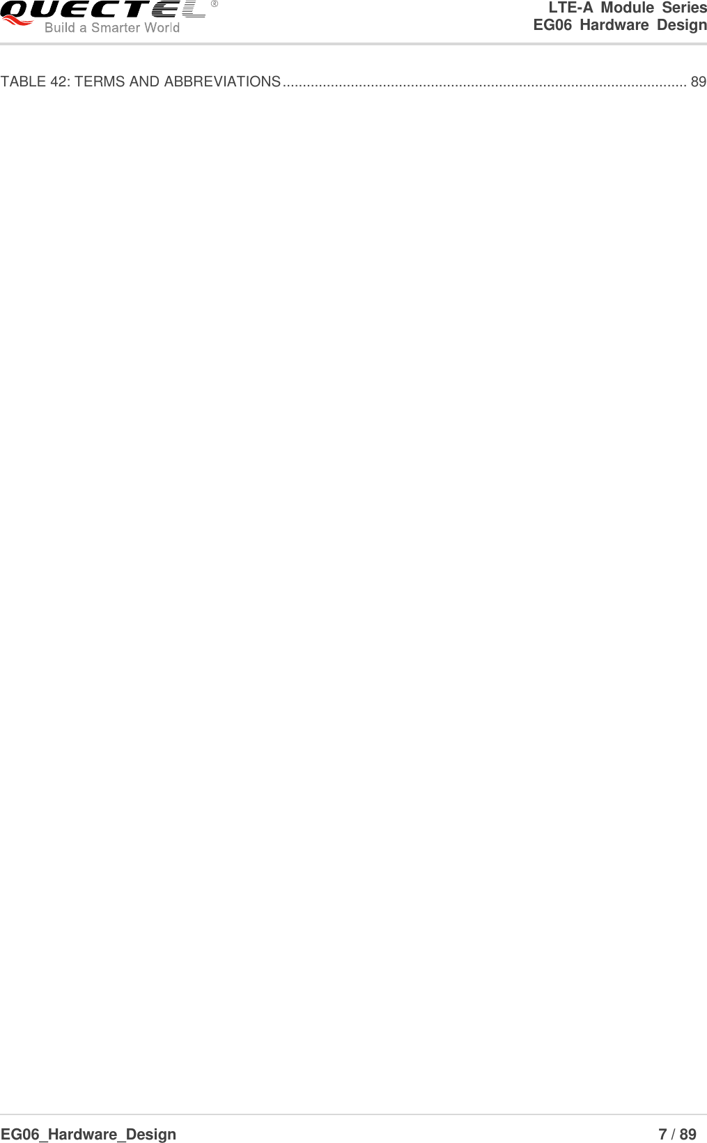
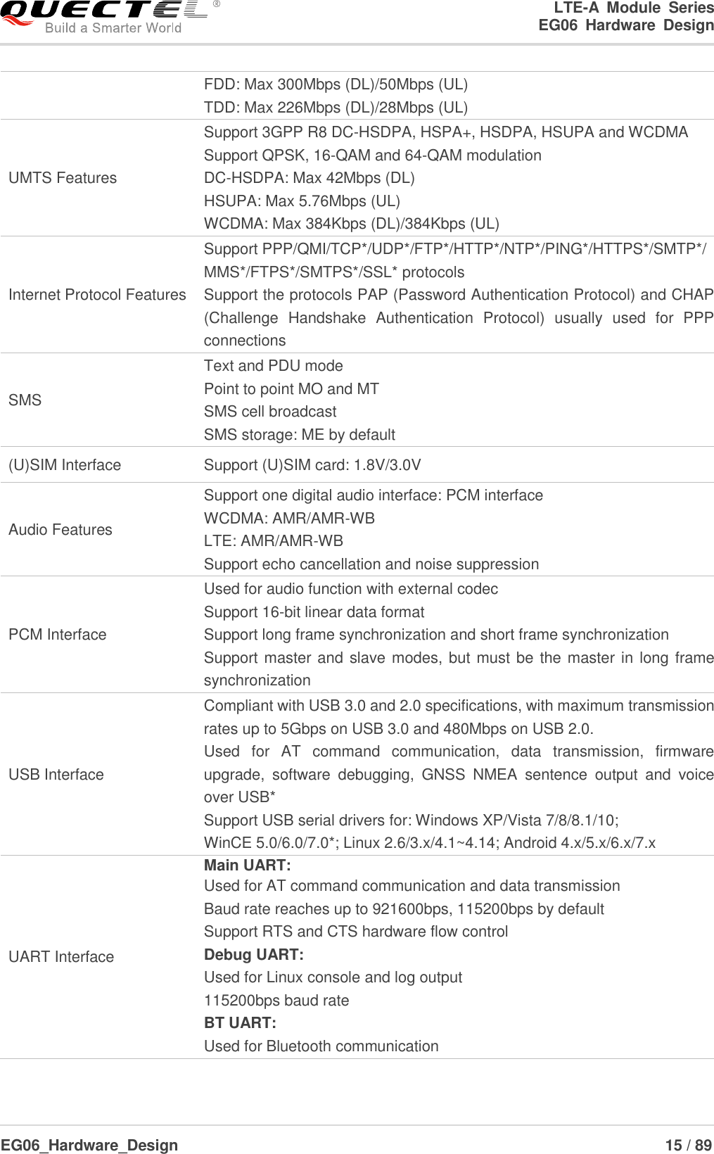
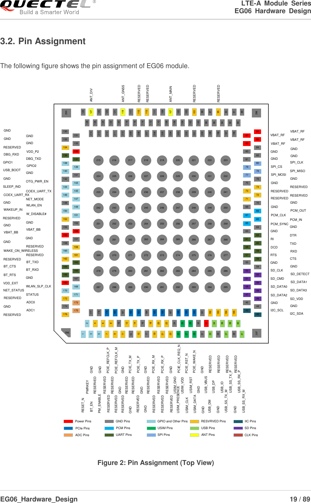
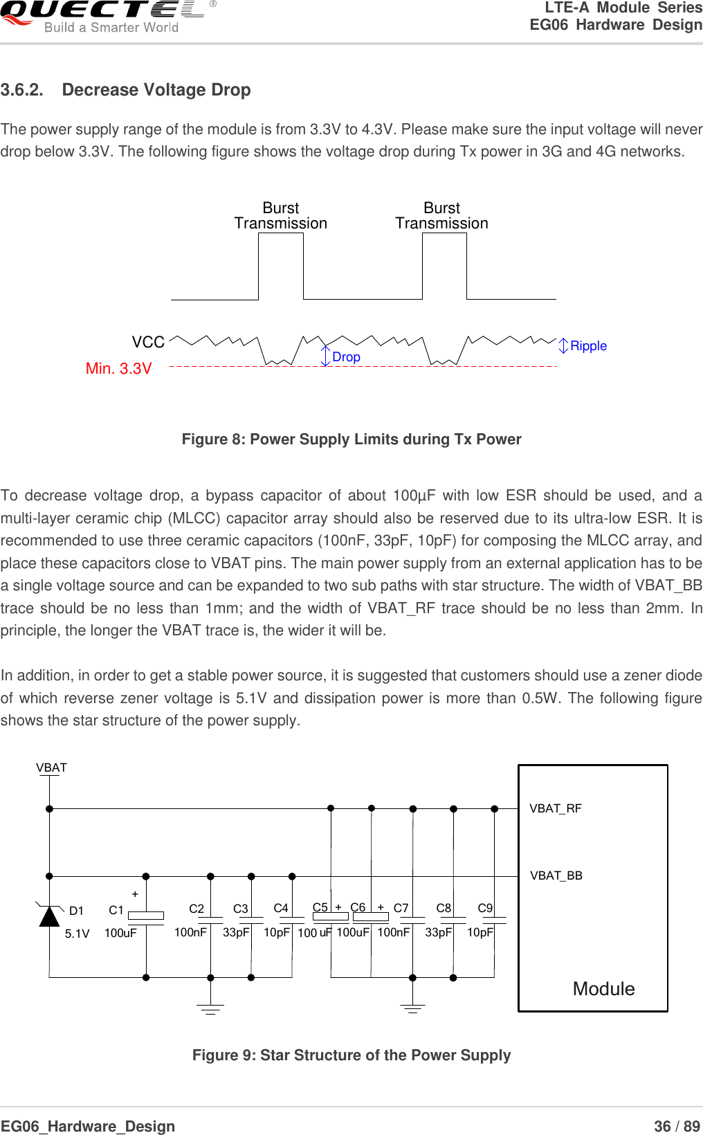
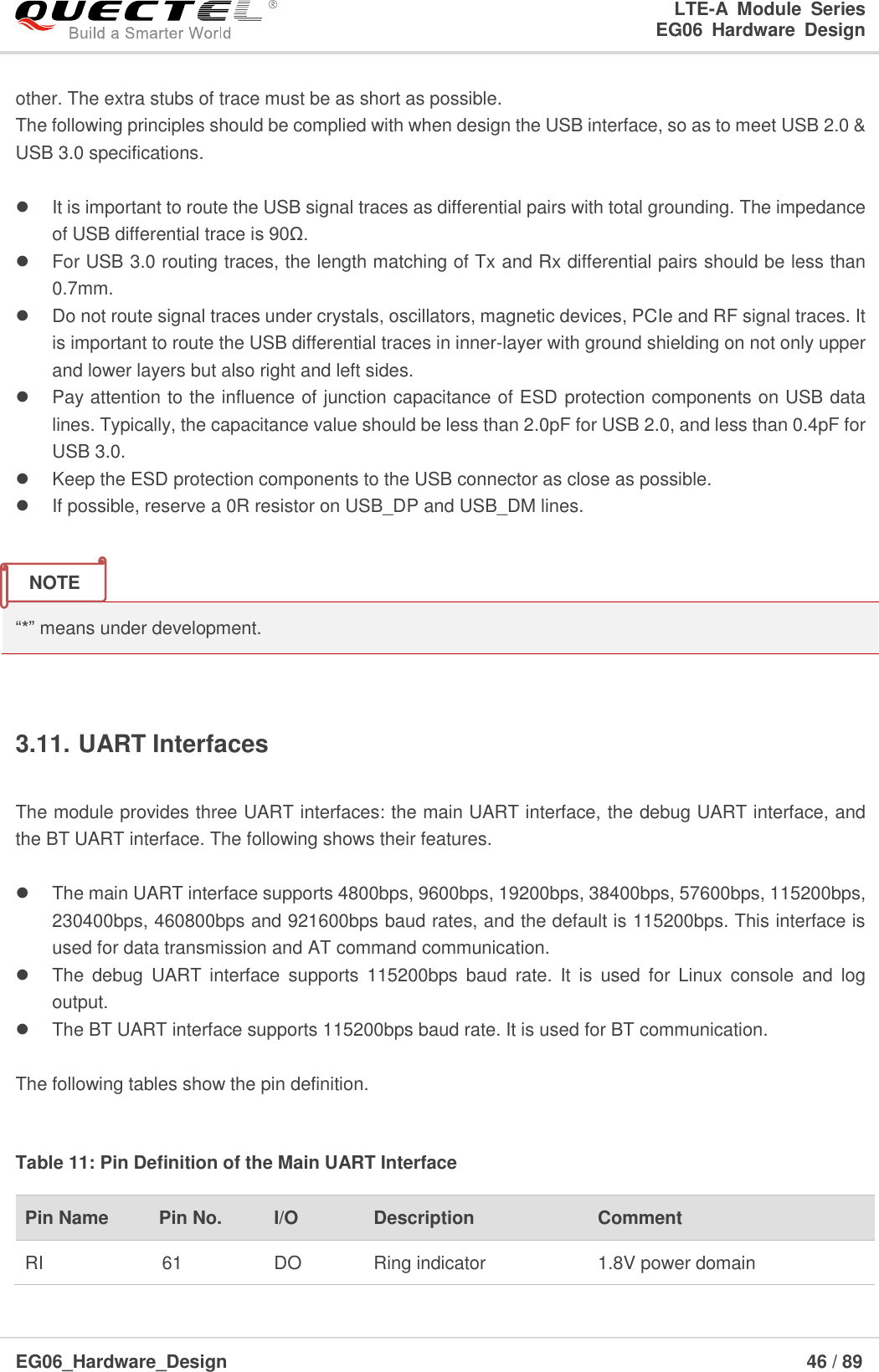
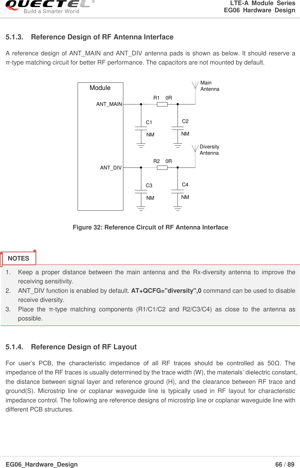
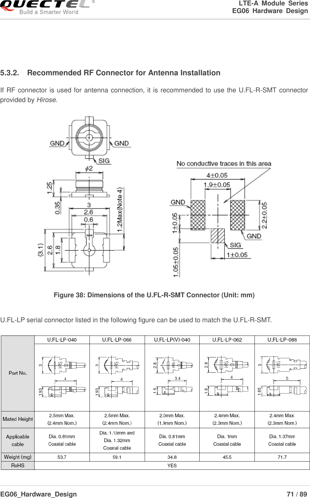
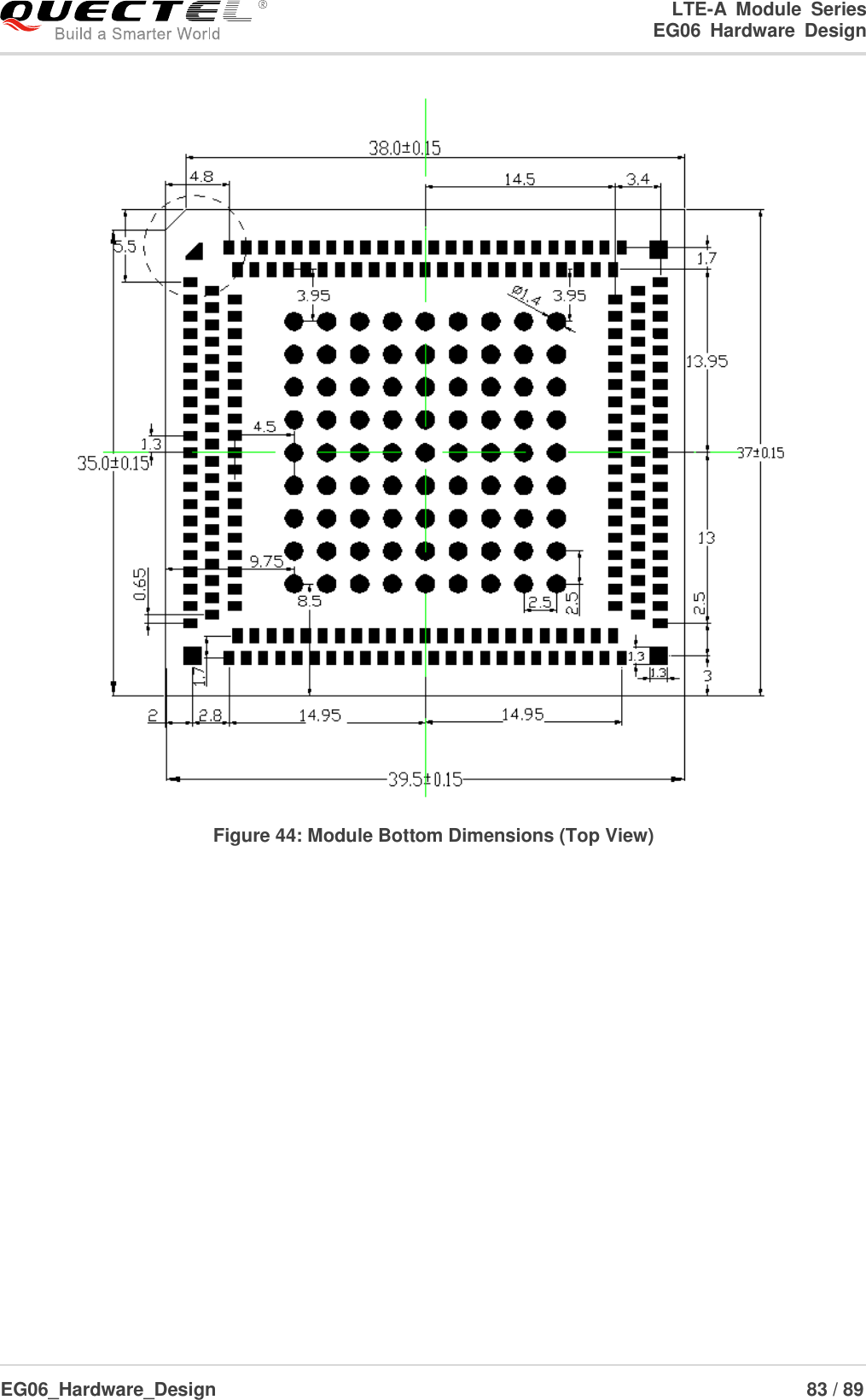
![LTE-A Module Series EG06 Hardware Design EG06_Hardware_Design 37 / 89 3.6.3. Reference Design for Power Supply Power design for the module is very important, as the performance of the module largely depends on the power source. The power supply of EG06 should be able to provide sufficient current up to 2A at least. If the voltage drop between the input and output is not too high, it is suggested that an LDO should be used to supply power for the module. If there is a big voltage difference between the input source and the desired output (VBAT), a buck converter is preferred to be used as the power supply. The following figure shows a reference design for +5V input power source. The designed output of the power supply is about 3.8V and the maximum load current is 3A. DC_INMIC29302WUIN OUTENGNDADJ2 4135VBAT 100nF 470uF 100nF100K47K470uF470R51K 1%1%4.7K47KVBAT_EN Figure 10: Reference Circuit of Power Supply In order to avoid damaging internal flash, please do not switch off the power supply when the module works normally. Only after the module is shut down by PWRKEY or AT command, the power supply can be cut off. 3.6.4. Monitor the Power Supply AT+CBC command can be used to monitor the VBAT_BB voltage value. For more details, please refer to document [1]. 3.7. Turn on and off Scenarios 3.7.1. Turn on Module Using the PWRKEY The following table shows the pin definition of PWRKEY. NOTE](https://usermanual.wiki/Quectel-Wireless-Solutions/201807EG06A/User-Guide-3944610-Page-39.png)
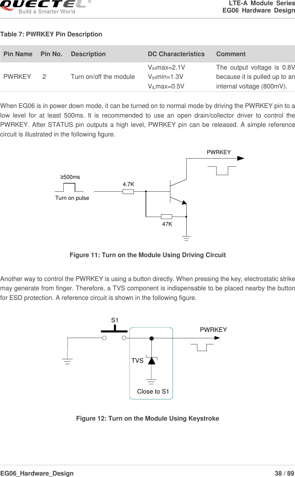
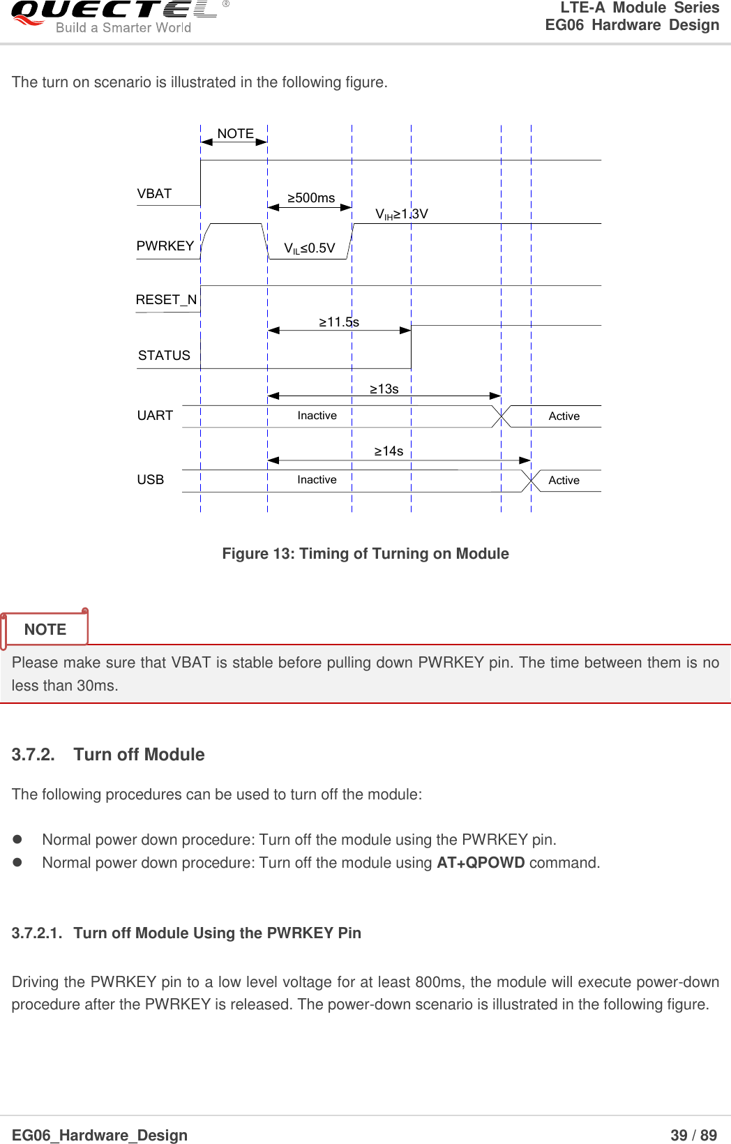
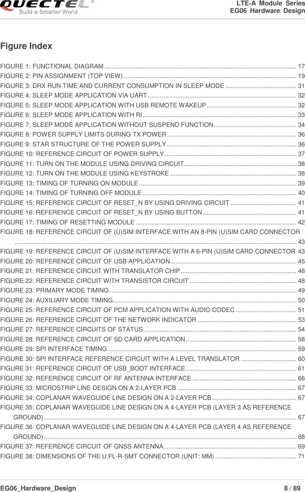
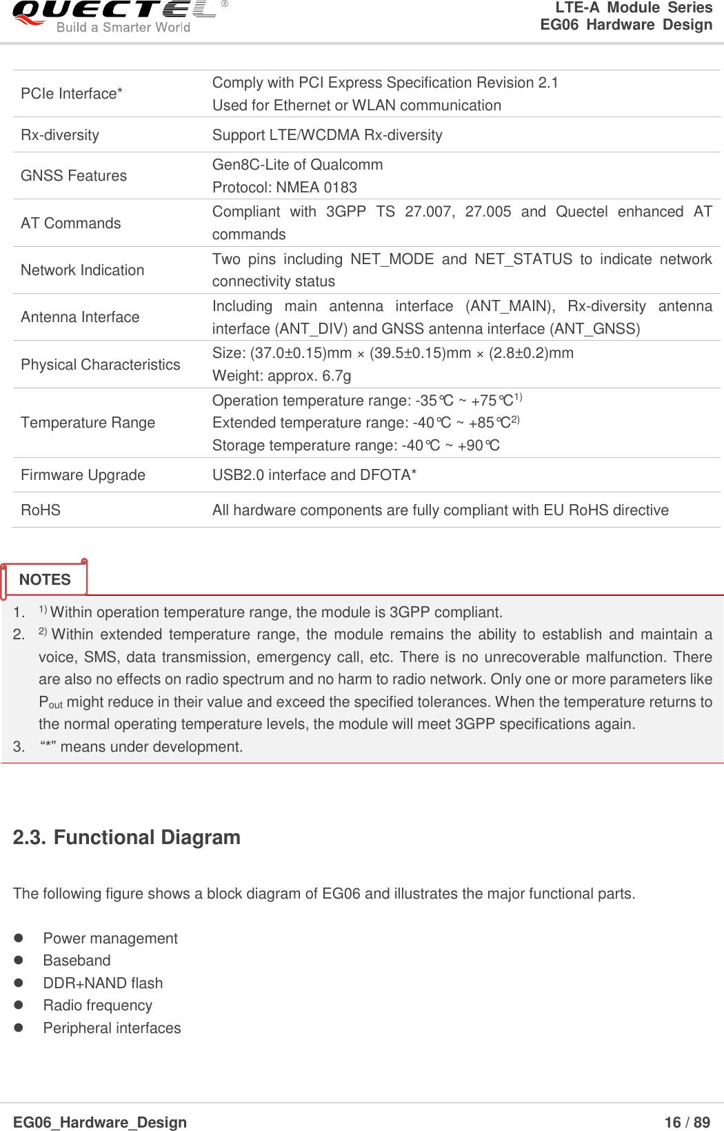
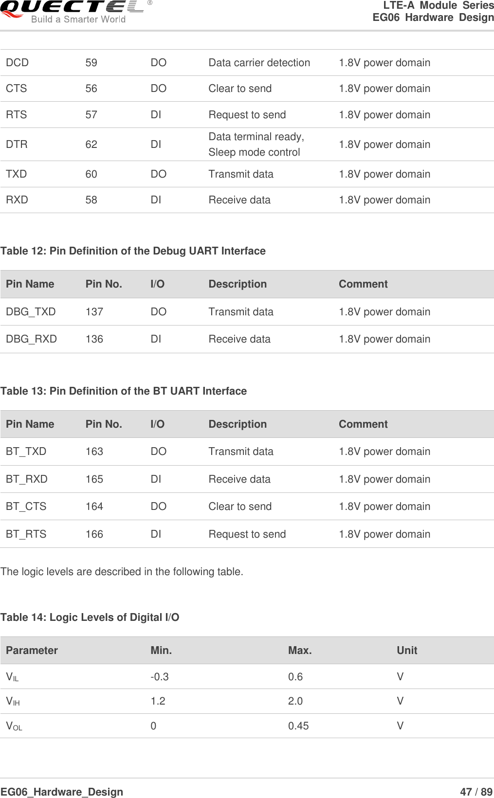
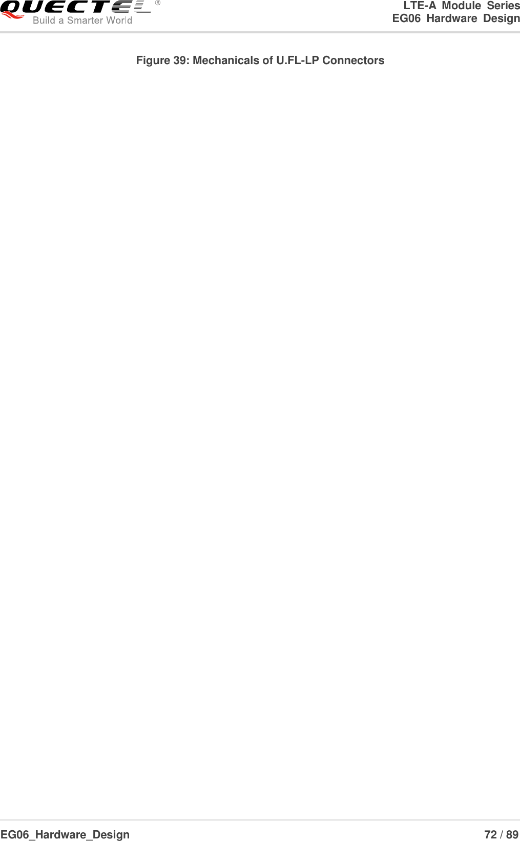
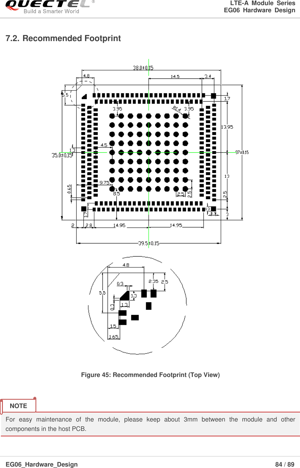
![LTE-A Module Series EG06 Hardware Design EG06_Hardware_Design 40 / 89 VBATPWRKEY≥800msRUNNING Power-down procedure OFFModuleStatusSTATUS≥30s Figure 14: Timing of Turning off Module 3.7.2.2. Turn off Module Using AT Command It is also a safe way to use AT+QPOWD command to turn off the module, which is similar to turning off the module via PWRKEY Pin. Please refer to document [1] for details about AT+QPOWD command. 1. In order to avoid damaging internal flash, please do not switch off the power supply when the module works normally. Only after the module is shut down by PWRKEY or AT command, the power supply can be cut off. 2. When turn off module with AT command, please keep PWRKEY at high level after the execution of power-off command. Otherwise the module will be turned on again after successfully turn-off. 3.8. Reset the Module The RESET_N pin can be used to reset the module. The module can be reset by driving the RESET_N to a low level voltage for 250ms~600ms. NOTES](https://usermanual.wiki/Quectel-Wireless-Solutions/201807EG06A/User-Guide-3944610-Page-42.png)
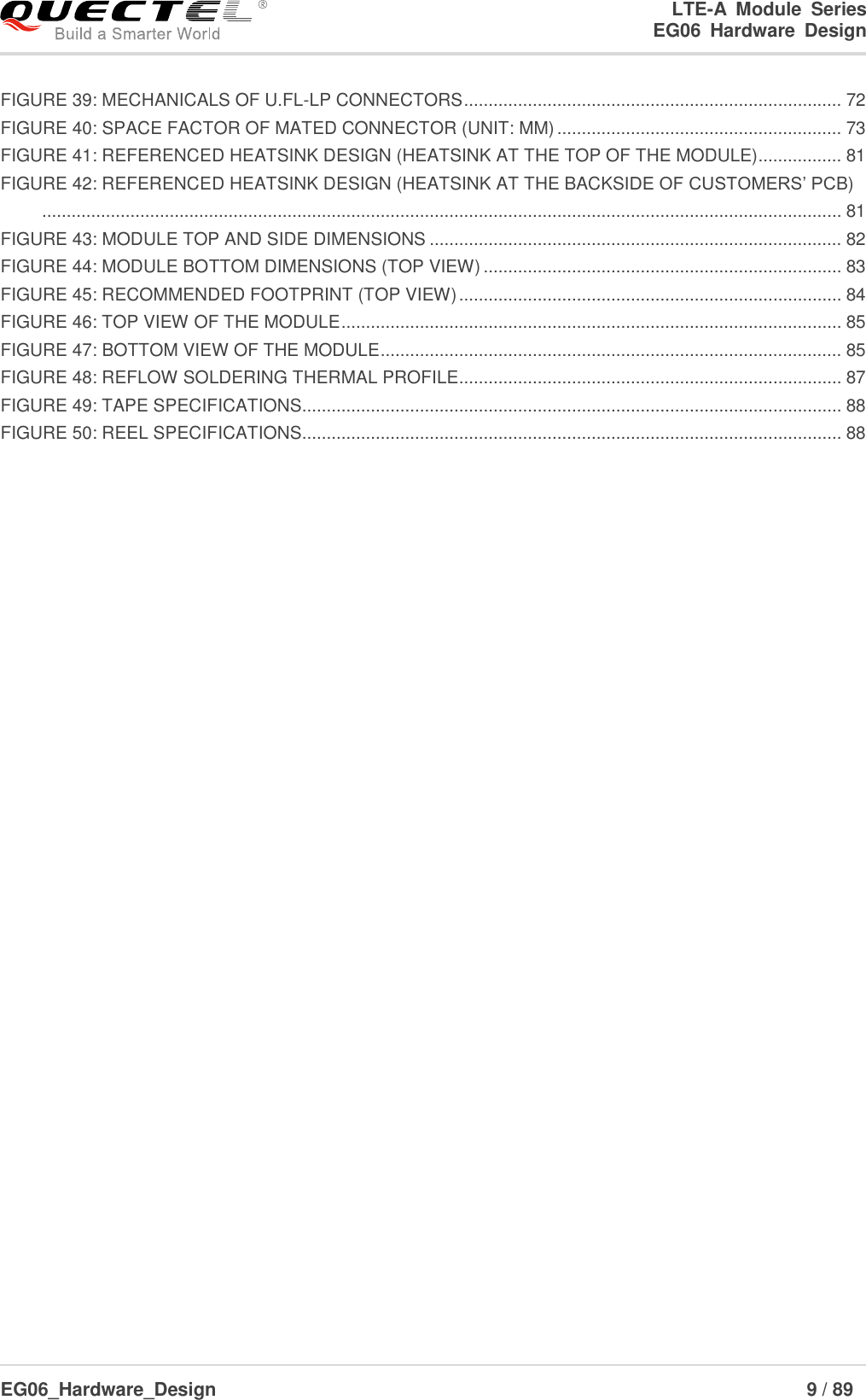
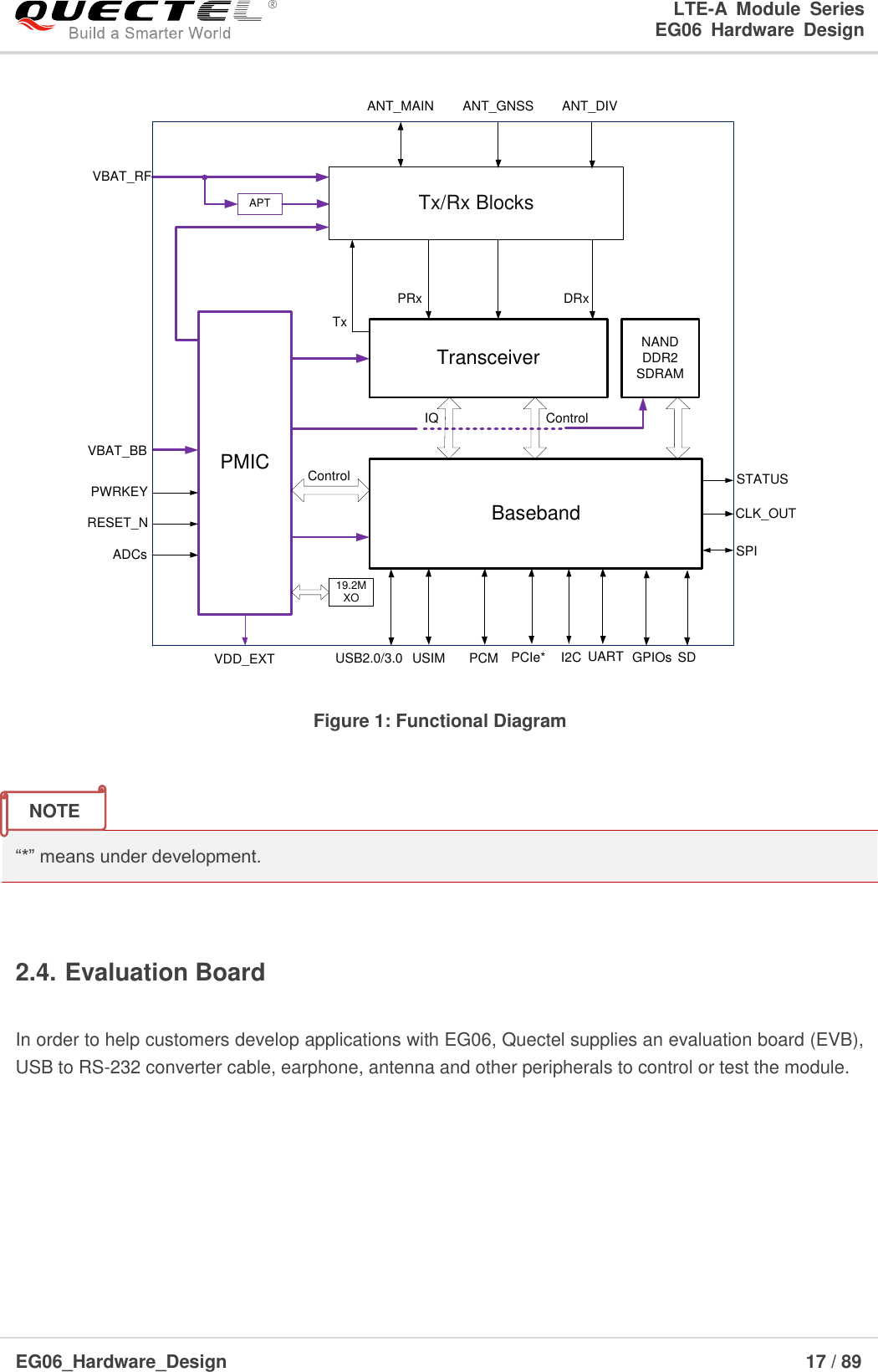
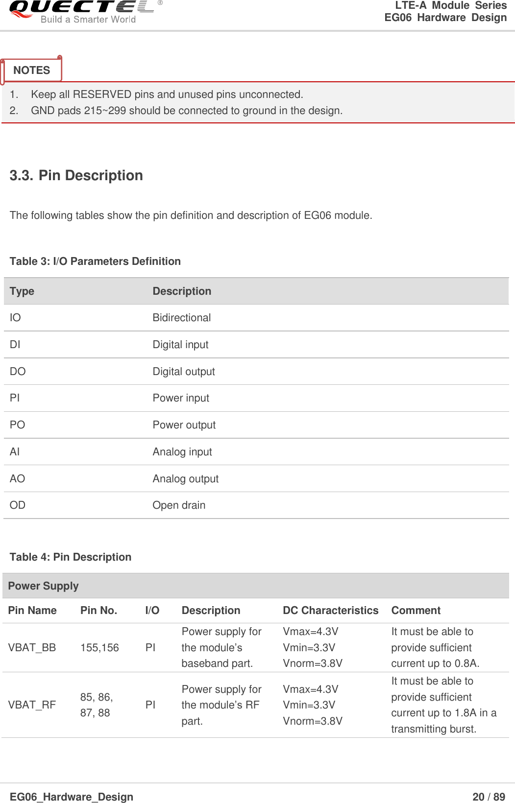
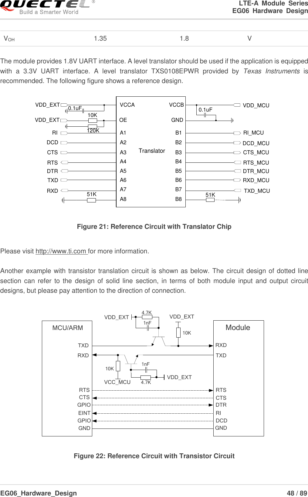
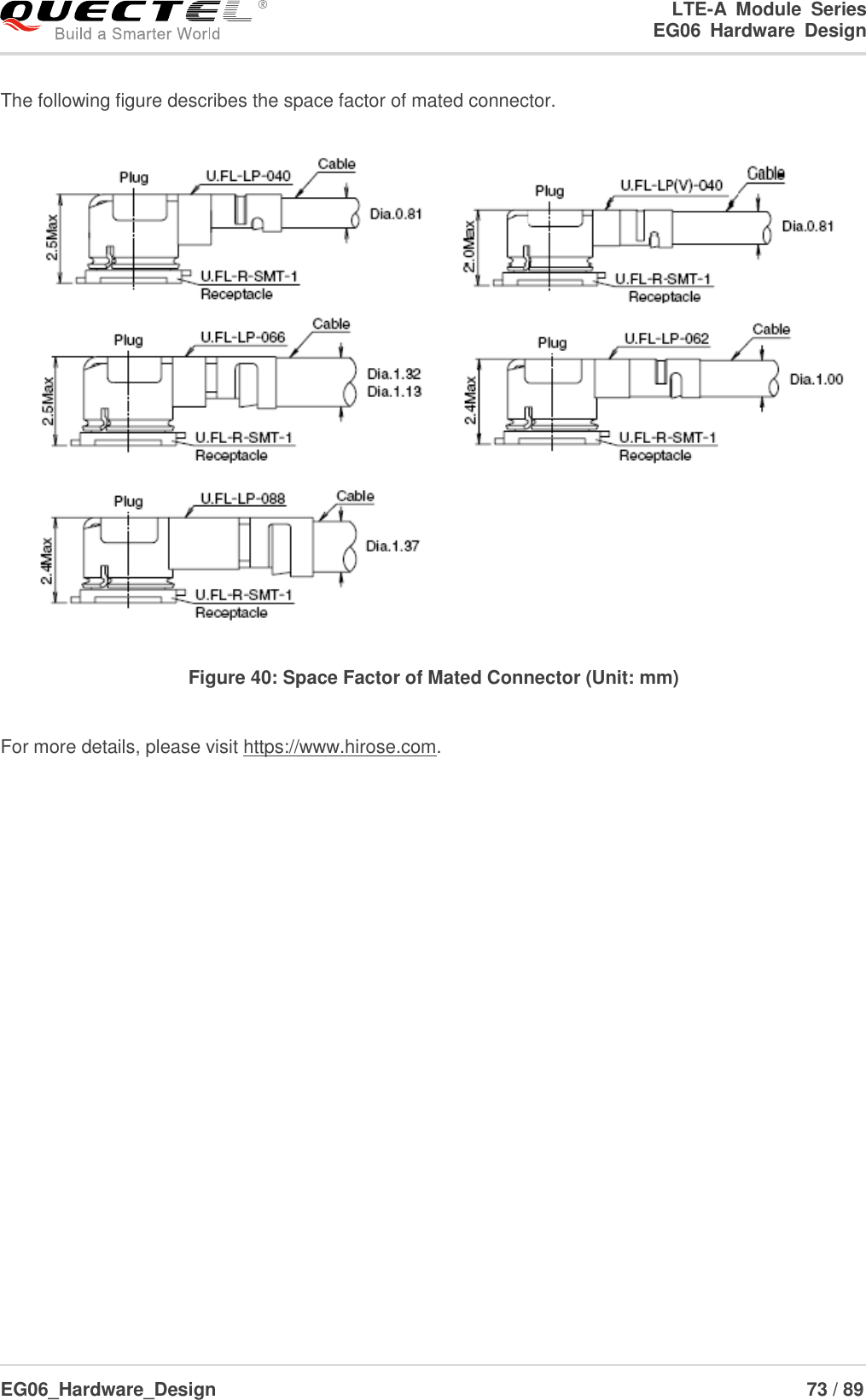
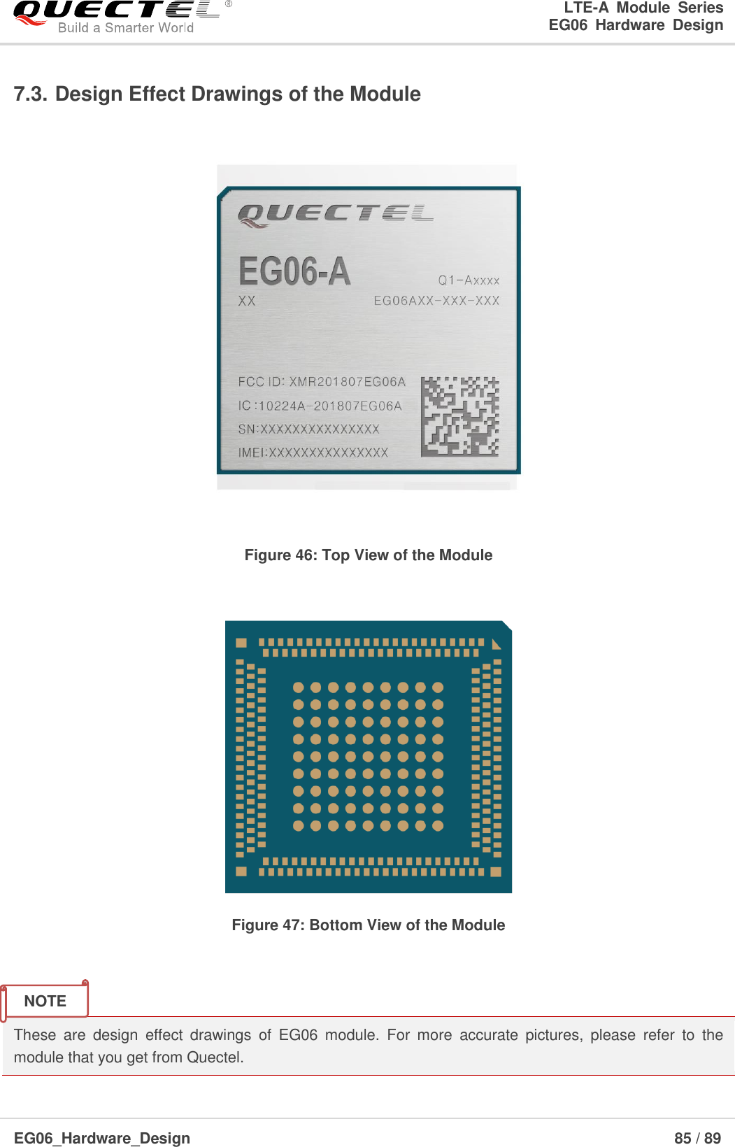
![LTE-A Module Series EG06 Hardware Design EG06_Hardware_Design 43 / 89 EG06 supports (U)SIM card hot-plug via the USIM_PRESENCE pin. The function supports low level and high level detections, and is disabled by default. Please refer to document [1] about AT+QSIMDET command for details. The following figure shows a reference design for (U)SIM card interface with an 8-pin (U)SIM card connector. ModuleUSIM_VDDUSIM_GNDUSIM_RSTUSIM_CLKUSIM_DATAUSIM_PRESENCE22R22R22RVDD_EXT51K100nF (U)SIM Card ConnectorGNDGNDVCCRSTCLK IOVPPGNDUSIM_VDD15KNM NM NM Figure 18: Reference Circuit of (U)SIM Interface with an 8-Pin (U)SIM Card Connector If (U)SIM card detection function is not needed, please keep USIM_PRESENCE unconnected. A reference circuit for (U)SIM interface with a 6-pin (U)SIM card connector is illustrated in the following figure. ModuleUSIM_VDDUSIM_GNDUSIM_RSTUSIM_CLKUSIM_DATA 22R22R22R100nF (U)SIM Card ConnectorGNDVCCRSTCLK IOVPPGND15KUSIM_VDDNM NMNM Figure 19: Reference Circuit of (U)SIM Interface with a 6-Pin (U)SIM Card Connector](https://usermanual.wiki/Quectel-Wireless-Solutions/201807EG06A/User-Guide-3944610-Page-45.png)
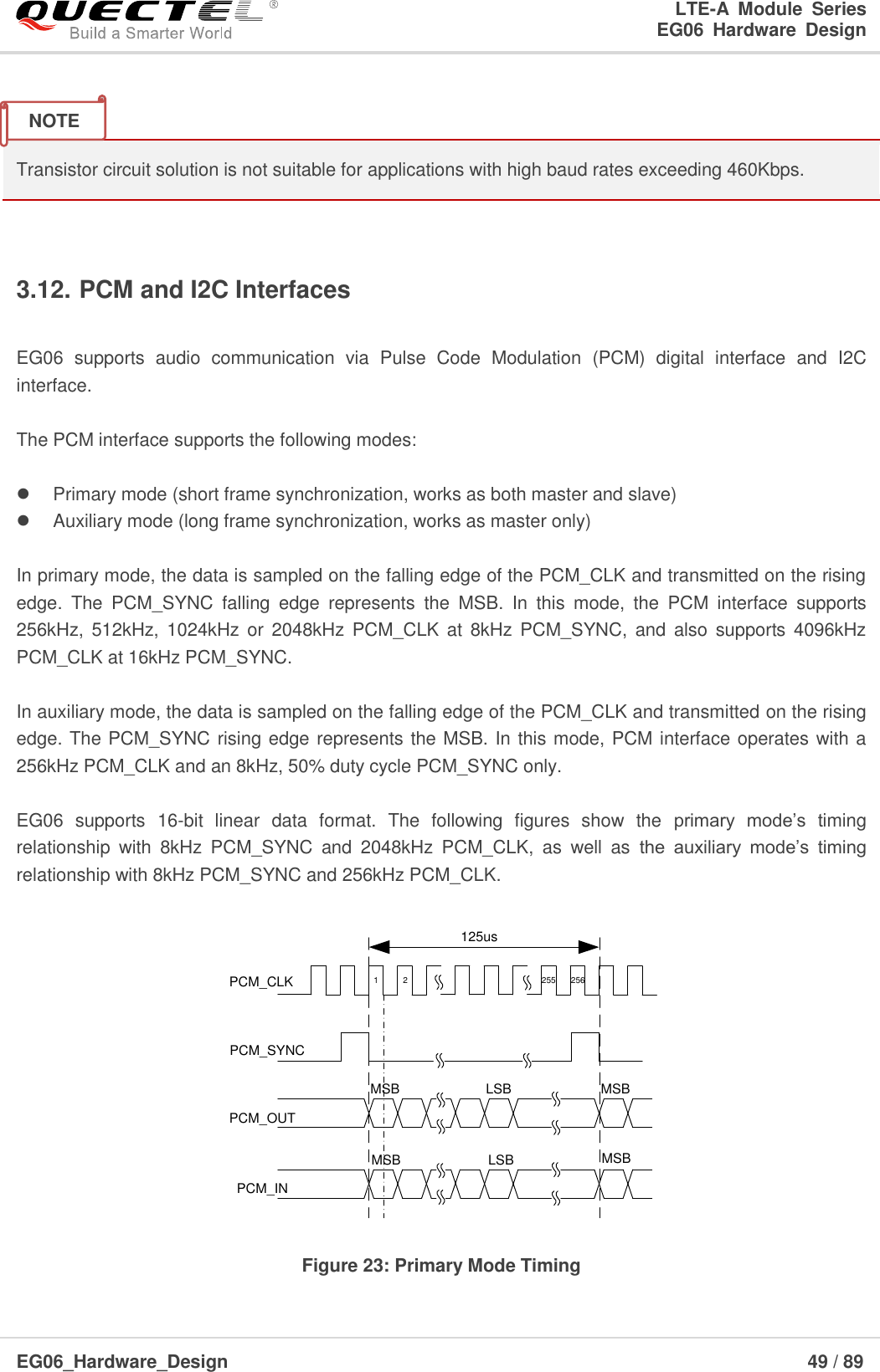
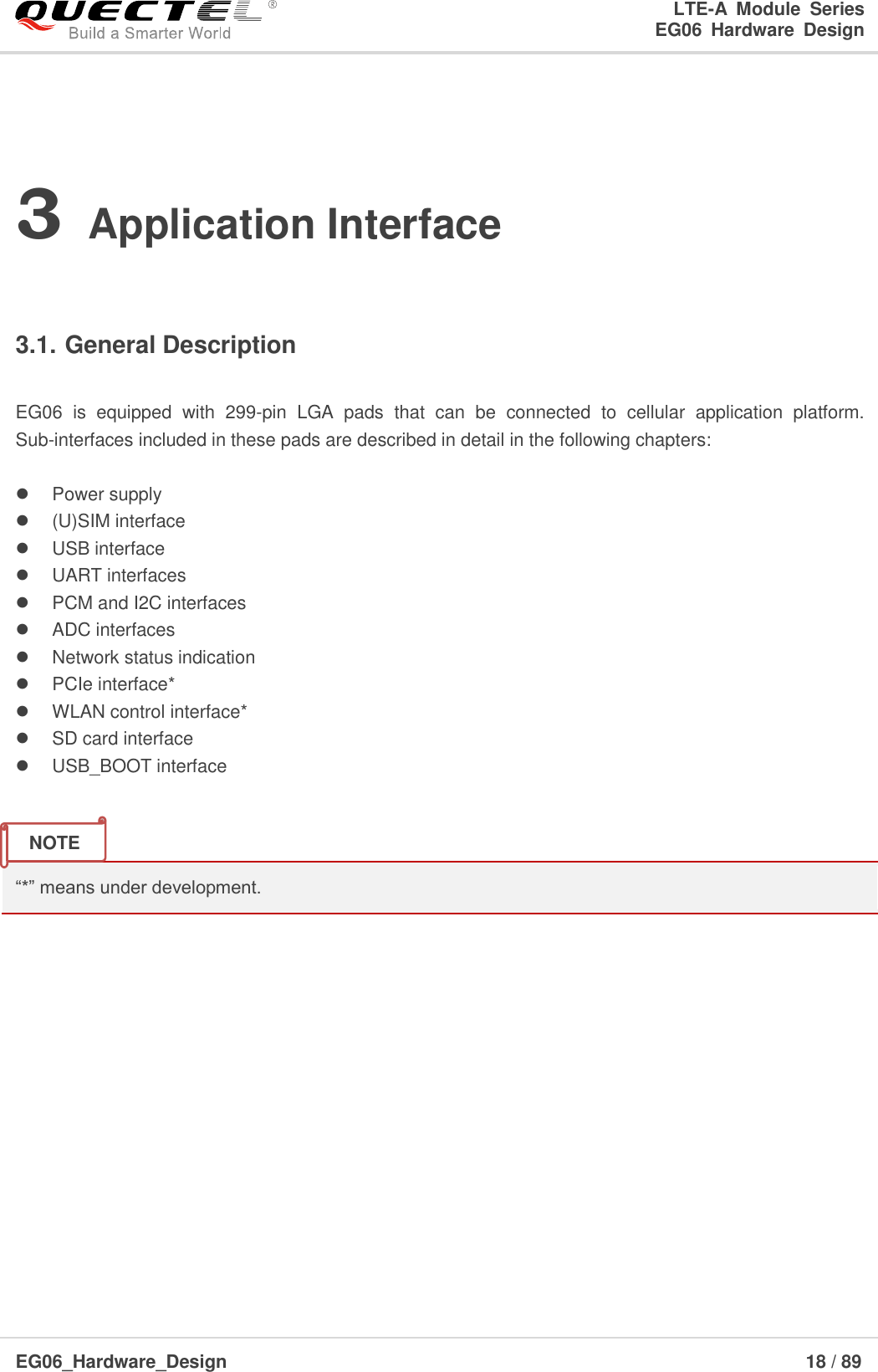
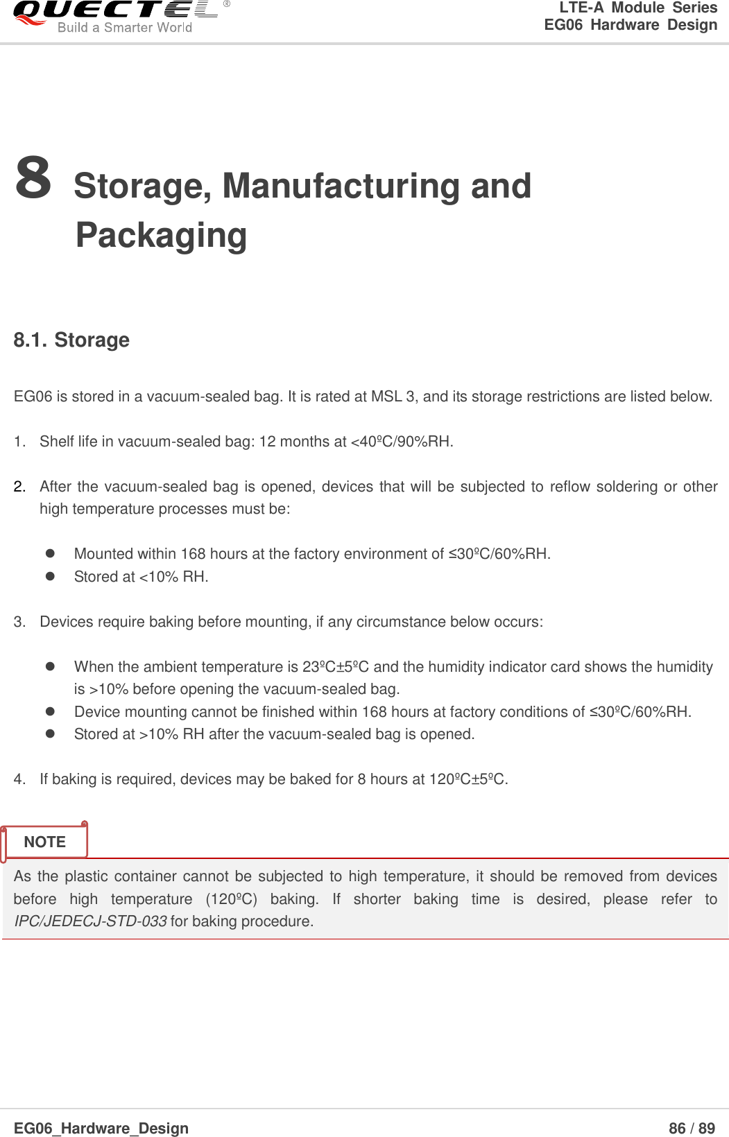
![LTE-A Module Series EG06 Hardware Design EG06_Hardware_Design 50 / 89 PCM_CLKPCM_SYNCPCM_OUTMSB LSBPCM_IN125usMSB1 2 3231LSB Figure 24: Auxiliary Mode Timing The following table shows the pin definition of PCM and I2C interfaces which can be applied on audio codec design. Table 15: Pin Definition of PCM and I2C Interfaces Clock and mode can be configured by AT command, and the default configuration is master mode using short frame synchronization format with 2048kHz PCM_CLK and 8kHz PCM_SYNC. Please refer to document [1] for details about AT+QDAI command. Pin Name Pin No. I/O Description Comment PCM_IN 66 DI PCM data input 1.8V power domain. If unused, keep it open. PCM_OUT 68 DO PCM data output 1.8V power domain. If unused, keep it open. PCM_SYNC 65 IO PCM data frame synchronization signal 1.8V power domain. In master mode, it is an output signal. In slave mode, it is an input signal. If unused, keep it open. PCM_CLK 67 IO PCM data bit clock 1.8V power domain. In master mode, it is an output signal. In slave mode, it is an input signal. If unused, keep it open. I2C_SCL 43 OD I2C serial clock Require an external pull-up to 1.8V I2C_SDA 42 OD I2C serial data Require an external pull-up to 1.8V](https://usermanual.wiki/Quectel-Wireless-Solutions/201807EG06A/User-Guide-3944610-Page-52.png)
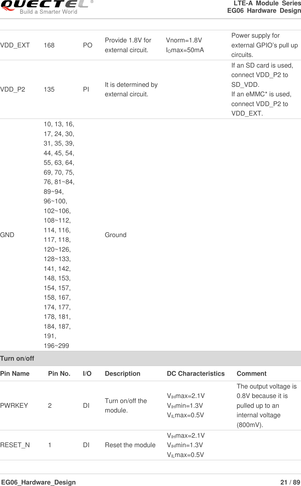
![LTE-A Module Series EG06 Hardware Design EG06_Hardware_Design 51 / 89 The following figure shows a reference design of PCM interface with an external codec IC. PCM_INPCM_OUTPCM_SYNCPCM_CLKI2C_SCLI2C_SDAModule1.8V4.7K4.7KBCLKLRCKDACADCSCLSDABIASMICBIASINPINNLOUTPLOUTNCodec Figure 25: Reference Circuit of PCM Application with Audio Codec 1. It is recommended to reserve an RC (R=22Ω, C=22pF) circuit on the PCM lines, especially for PCM_CLK. 2. EG06 works as a master device pertaining to I2C interface. 3.13. ADC Interfaces The module provides two Analog-to-Digital Converters (ADC) interfaces. AT+QADC=0 command can be used to read the voltage value on ADC0 pin. AT+QADC=1 command can be used to read the voltage value on ADC1 pin. For more details about these AT+QADC command, please refer to document [1]. In order to improve the accuracy of ADC, the trace of ADC should be surrounded by ground. Table 16: Pin Definition of the ADC Interfaces Pin Name Pin No. Description ADC0 173 General purpose analog to digital converter ADC1 175 General purpose analog to digital converter NOTES](https://usermanual.wiki/Quectel-Wireless-Solutions/201807EG06A/User-Guide-3944610-Page-53.png)
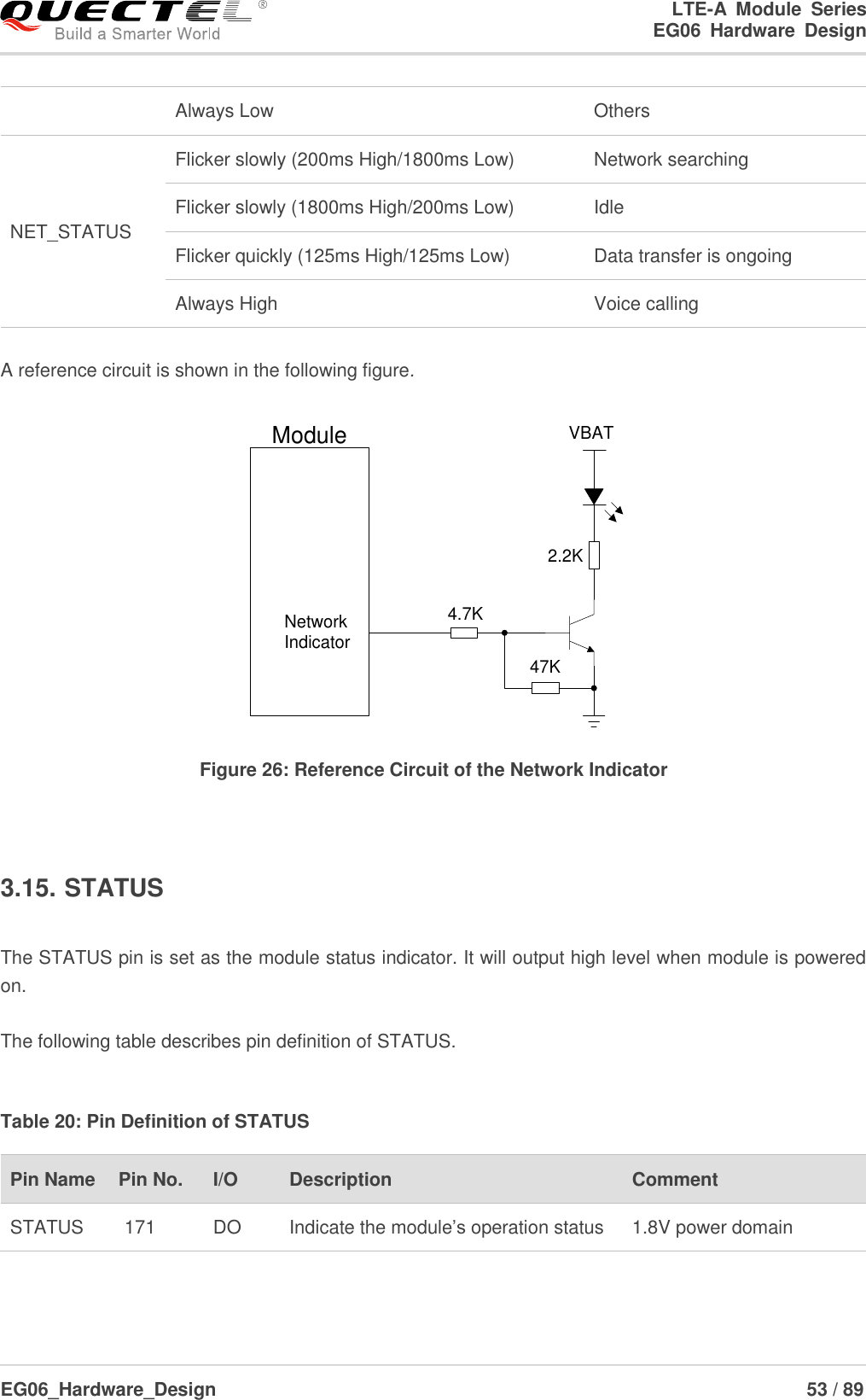
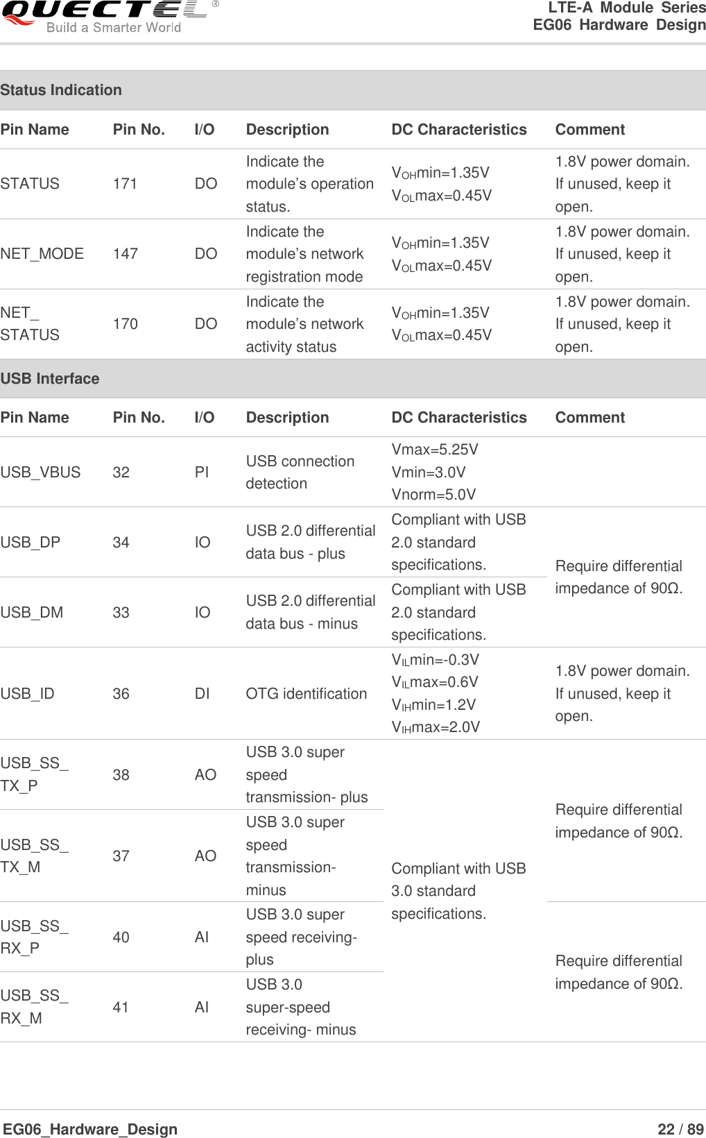
![LTE-A Module Series EG06 Hardware Design EG06_Hardware_Design 54 / 89 A reference circuit is shown as below. 4.7K47KVBAT2.2KModule STATUS Figure 27: Reference Circuits of STATUS 3.16. Behavior of the RI AT+QCFG="risignaltype","physical" command can be used to configure RI behavior. No matter on which port a URC is presented, the URC will trigger the behavior of RI pin. The URC can be output from UART port, USB AT port and USB modem port by AT+QURCCFG command. The default port is USB AT port. In addition, RI behavior can be configured flexibly. The default behavior of the RI is shown as below. Table 21: Behavior of the RI State Response Idle RI keeps at high level URC RI outputs 120ms low pulse when a new URC returns The RI behavior can be changed by AT+QCFG="urc/ri/ring" command. Please refer to document [1] for details. NOTE](https://usermanual.wiki/Quectel-Wireless-Solutions/201807EG06A/User-Guide-3944610-Page-56.png)
![LTE-A Module Series EG06 Hardware Design EG06_Hardware_Design 62 / 89 4 GNSS Receiver 4.1. General Description EG06 includes a fully integrated global navigation satellite system solution that supports Gen8C-Lite of Qualcomm (GPS, GLONASS, BeiDou, Galileo and QZSS). EG06 supports standard NMEA-0183 protocol, and outputs NMEA sentences at 1Hz data update rate via USB interface by default. By default, EG06 GNSS engine is switched off. It has to be switched on via AT command. For more details about GNSS engine technology and configurations, please refer to document [2]. 4.2. GNSS Performance The following table shows GNSS performance of EG06. Table 28: GNSS Performance Parameter Description Conditions Typ. Unit Sensitivity (GNSS) Cold start Autonomous TBD dBm Reacquisition Autonomous TBD dBm Tracking Autonomous TBD dBm TTFF (GNSS) Cold start @open sky Autonomous TBD s XTRA enabled TBD s Warm start @open sky Autonomous TBD s XTRA enabled TBD s](https://usermanual.wiki/Quectel-Wireless-Solutions/201807EG06A/User-Guide-3944610-Page-64.png)
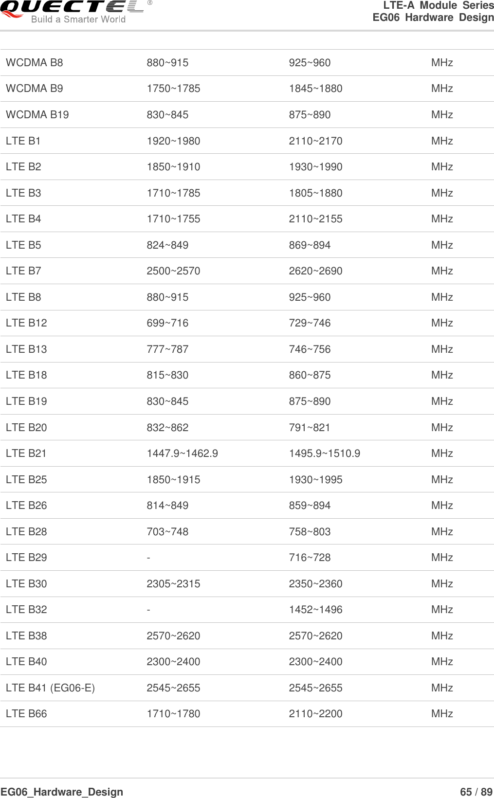
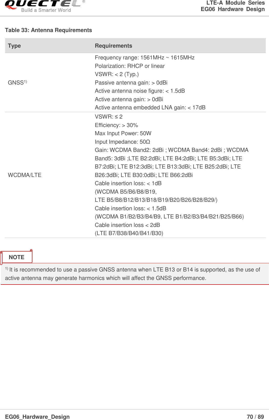
![LTE-A Module Series EG06 Hardware Design EG06_Hardware_Design 68 / 89 Figure 36: Coplanar Waveguide Line Design on a 4-layer PCB (Layer 4 as Reference Ground) In order to ensure RF performance and reliability, the following principles should be complied with in RF layout design: Use impedance simulation tool to control the characteristic impedance of RF traces as 50Ω. The GND pins adjacent to RF pins should not be designed as thermal relief pads, and should be fully connected to ground. The distance between the RF pins and the RF connector should be as short as possible, and all the right angle traces should be changed to curved ones. There should be clearance area under the signal pin of the antenna connector or solder joint. The reference ground of RF traces should be complete. Meanwhile, adding some ground vias around RF traces and the reference ground could help to improve RF performance. The distance between the ground vias and RF traces should be no less than two times the width of RF signal traces (2*W). For more details about RF layout, please refer to document [5]. 5.2. GNSS Antenna Interface The following tables show pin definition and frequency specification of GNSS antenna interface. Table 31: Pin Definition of GNSS Antenna Interface Pin Name Pin No. I/O Description Comment ANT_GNSS 119 AI GNSS antenna pad 50Ω impedance](https://usermanual.wiki/Quectel-Wireless-Solutions/201807EG06A/User-Guide-3944610-Page-70.png)
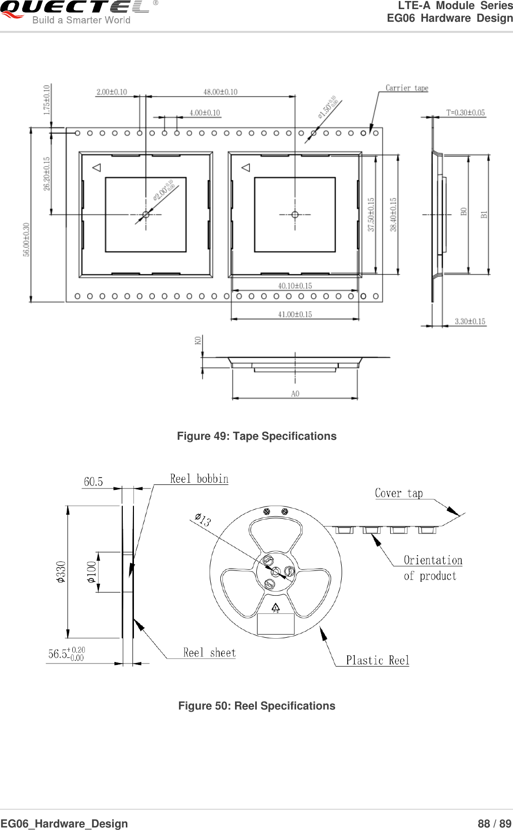
![LTE-A Module Series EG06 Hardware Design EG06_Hardware_Design 87 / 89 8.2. Manufacturing and Soldering Push the squeegee to apply the solder paste on the surface of stencil, thus making the paste fill the stencil openings and then penetrate to the PCB. The force on the squeegee should be adjusted properly so as to produce a clean stencil surface on a single pass. To ensure the module soldering quality, the thickness of stencil for the module should be 0.18mm. For more details, please refer to document [3]. It is suggested that the peak reflow temperature is 235ºC ~ 245ºC (for SnAg3.0Cu0.5 alloy). The absolute max reflow temperature is 260ºC. To avoid damage to the module caused by repeated heating, it is suggested that the module should be mounted after reflow soldering for the other side of PCB has been completed. Recommended reflow soldering thermal profile is shown below: Time50 100 150 200 250 30050100150200250 160ºC 200ºC217070s~120s40s~60sBetween 1~3ºC/sPreheat Heating CoolingºCsLiquids Temperature Temperature Figure 48: Reflow Soldering Thermal Profile 8.3. Packaging EG06 is packaged in tape and reel carriers. One reel is 10.56 meters long and contains 200 modules. The figures below show the packaging details, measured in mm.](https://usermanual.wiki/Quectel-Wireless-Solutions/201807EG06A/User-Guide-3944610-Page-89.png)
![LTE Module Sires EG06Hardware Design EG06_Hardware_Design 89 / 89 9 Appendix A References Table 41: Related Documents Table 42: Terms and Abbreviations SN Document Name Remark [1] Quectel_Ex06_AT_Commands_Manual EG06 AT Commands Manual [2] Quectel_Ex06_GNSS_AT_Commands_ Manual EG06 GNSS AT Commands Manual [3] Quectel_Module_Secondary_SMT_User_Guide Module Secondary SMT User Guide [4] Quectel_EG06_Reference_Design EG06 Reference Design [5] Quectel_RF_Layout_Application_Note RF Layout Application Note Abbreviation Description AMR Adaptive Multi-rate bps Bits Per Second CHAP Challenge Handshake Authentication Protocol CS Coding Scheme CSD Circuit Switched Data CTS Clear To Send DC-HSPA+ Dual-carrier High Speed Packet Access DFOTA Delta Firmware Upgrade Over The Air DL Downlink DTR Data Terminal Ready](https://usermanual.wiki/Quectel-Wireless-Solutions/201807EG06A/User-Guide-3944610-Page-91.png)