Quectel Wireless Solutions 201807EG06A LTE-A Cat6 Module User Manual
Quectel Wireless Solutions Company Limited LTE-A Cat6 Module Users Manual
Users Manual

EG06 Manual
LTE-A Module Series
Rev. EG06_Hardware_Design_V1.0
Date: 2018-05-16
Status: Released

LTE-A Module Series
EG06 Hardware Design
EG06_Hardware_Design 1 / 89
Our aim is to provide customers with timely and comprehensive service. For any
assistance, please contact our company headquarters:
Quectel Wireless Solutions Co., Ltd.
7th Floor, Hongye Building, No.1801 Hongmei Road, Xuhui District, Shanghai 200233, China
Tel: +86 21 5108 6236
Email: info@quectel.com
Or our local office. For more information, please visit:
http://quectel.com/support/sales.htm
For technical support, or to report documentation errors, please visit:
http://quectel.com/support/technical.htm
Or Email to: support@quectel.com
GENERAL NOTES
QUECTEL OFFERS THE INFORMATION AS A SERVICE TO ITS CUSTOMERS. THE INFORMATION
PROVIDED IS BASED UPON CUSTOMERS’ REQUIREMENTS. QUECTEL MAKES EVERY EFFORT
TO ENSURE THE QUALITY OF THE INFORMATION IT MAKES AVAILABLE. QUECTEL DOES NOT
MAKE ANY WARRANTY AS TO THE INFORMATION CONTAINED HEREIN, AND DOES NOT ACCEPT
ANY LIABILITY FOR ANY INJURY, LOSS OR DAMAGE OF ANY KIND INCURRED BY USE OF OR
RELIANCE UPON THE INFORMATION. ALL INFORMATION SUPPLIED HEREIN IS SUBJECT TO
CHANGE WITHOUT PRIOR NOTICE.
COPYRIGHT
THE INFORMATION CONTAINED HERE IS PROPRIETARY TECHNICAL INFORMATION OF
QUECTEL WIRELESS SOLUTIONS CO., LTD. TRANSMITTING, REPRODUCTION, DISSEMINATION
AND EDITING OF THIS DOCUMENT AS WELL AS UTILIZATION OF THE CONTENT ARE
FORBIDDEN WITHOUT PERMISSION. OFFENDERS WILL BE HELD LIABLE FOR PAYMENT OF
DAMAGES. ALL RIGHTS ARE RESERVED IN THE EVENT OF A PATENT GRANT OR
REGISTRATION OF A UTILITY MODEL OR DESIGN.
Copyright © Quectel Wireless Solutions Co., Ltd. 2018. All rights reserved

LTE-A Module Series
EG06 Hardware Design
EG06_Hardware_Design 2 / 89
About the Document
History
Revision
Date
Author
Description
1.0
2018-04-11
King MA/
Wison HE
Initial

LTE-A Module Series
EG06 Hardware Design
EG06_Hardware_Design 3 / 89
Contents
About the Document ................................................................................................................................... 2
Contents ....................................................................................................................................................... 3
Table Index ................................................................................................................................................... 6
Figure Index ................................................................................................................................................. 8
1 Introduction ........................................................................................................................................ 10
1.1. Safety Information.................................................................................................................... 11
2 Product Concept ................................................................................................................................ 13
2.1. General Description ................................................................................................................. 13
2.2. Key Features ........................................................................................................................... 14
2.3. Functional Diagram ................................................................................................................. 16
2.4. Evaluation Board ..................................................................................................................... 17
3 Application Interface ......................................................................................................................... 18
3.1. General Description ................................................................................................................. 18
3.2. Pin Assignment ........................................................................................................................ 19
3.3. Pin Description ......................................................................................................................... 20
3.4. Operating Modes ..................................................................................................................... 30
3.5. Power Saving ........................................................................................................................... 31
3.5.1. Sleep Mode .................................................................................................................... 31
3.5.1.1. UART Application ................................................................................................. 31
3.5.1.2. USB Application with USB Remote Wakeup Function ........................................ 32
3.5.1.3. USB Application with USB Suspend/Resume and RI Function .......................... 33
3.5.1.4. USB Application without USB Suspend Function ................................................ 33
3.5.2. Airplane Mode ................................................................................................................ 34
3.6. Power Supply ........................................................................................................................... 35
3.6.1. Power Supply Pins ......................................................................................................... 35
3.6.2. Decrease Voltage Drop .................................................................................................. 36
3.6.3. Reference Design for Power Supply .............................................................................. 37
3.6.4. Monitor the Power Supply .............................................................................................. 37
3.7. Turn on and off Scenarios ....................................................................................................... 37
3.7.1. Turn on Module Using the PWRKEY ............................................................................. 37
3.7.2. Turn off Module .............................................................................................................. 39
3.7.2.1. Turn off Module Using the PWRKEY Pin ............................................................ 39
3.7.2.2. Turn off Module Using AT Command .................................................................. 40
3.8. Reset the Module..................................................................................................................... 40
3.9. (U)SIM Interface ...................................................................................................................... 42
3.10. USB Interface .......................................................................................................................... 44
3.11. UART Interfaces ...................................................................................................................... 46
3.12. PCM and I2C Interfaces .......................................................................................................... 49
3.13. ADC Interfaces ........................................................................................................................ 51
3.14. Network Status Indication ........................................................................................................ 52
3.15. STATUS ................................................................................................................................... 53

LTE-A Module Series
EG06 Hardware Design
EG06_Hardware_Design 4 / 89
3.16. Behavior of the RI .................................................................................................................... 54
3.17. PCIe Interface* ........................................................................................................................ 55
3.18. WLAN Control Interface* ......................................................................................................... 56
3.19. SD Card Interface .................................................................................................................... 57
3.20. SPI Interface ............................................................................................................................ 59
3.21. USB_BOOT Interface .............................................................................................................. 60
4 GNSS Receiver ................................................................................................................................... 62
4.1. General Description ................................................................................................................. 62
4.2. GNSS Performance ................................................................................................................. 62
4.3. Layout Guidelines .................................................................................................................... 63
5 Antenna Interfaces ............................................................................................................................. 64
5.1. Main/Rx-diversity Antenna Interface ....................................................................................... 64
5.1.1. Pin Definition .................................................................................................................. 64
5.1.2. Operating Frequency ..................................................................................................... 64
5.1.3. Reference Design of RF Antenna Interface ................................................................... 66
5.1.4. Reference Design of RF Layout..................................................................................... 66
5.2. GNSS Antenna Interface ......................................................................................................... 68
5.3. Antenna Installation ................................................................................................................. 69
5.3.1. Antenna Requirement .................................................................................................... 69
5.3.2. Recommended RF Connector for Antenna Installation ................................................. 71
6 Electrical, Reliability and Radio Characteristics ............................................................................ 74
6.1. Absolute Maximum Ratings ..................................................................................................... 74
6.2. Power Supply Ratings ............................................................................................................. 75
6.3. Operation and Storage Temperatures .................................................................................... 75
6.4. Current Consumption .............................................................................................................. 76
6.5. RF Output Power ..................................................................................................................... 78
6.6. RF Receiving Sensitivity .......................................................................................................... 78
6.7. Electrostatic Discharge ............................................................................................................ 79
6.8. Thermal Consideration ............................................................................................................ 80
7 Mechanical Dimensions .................................................................................................................... 82
7.1. Mechanical Dimensions of the Module.................................................................................... 82
7.2. Recommended Footprint ......................................................................................................... 84
7.3. Design Effect Drawings of the Module .................................................................................... 85
8 Storage, Manufacturing and Packaging .......................................................................................... 86
8.1. Storage .................................................................................................................................... 86
8.2. Manufacturing and Soldering .................................................................................................. 87
8.3. Packaging ................................................................................................................................ 87
9 Appendix A References ..................................................................................................................... 89
10 IC & FCC Requirement ...................................................................................................................... 93
10.1. FCC Regulations: .................................................................................................................... 93
10.2. RF Exposure Information ......................................................................................................... 93
10.3. ISED Notice ............................................................................................................................. 93
10.4. ISED Radiation Exposure Statement ...................................................................................... 94
10.5. IMPORTANT NOTE: ............................................................................................................... 94

LTE-A Module Series
EG06 Hardware Design
EG06_Hardware_Design 5 / 89
10.6. USERS MANUAL OF THE END PRODUCT: ......................................................................... 94
10.7. LABEL OF THE END PRODUCT: ........................................................................................... 95

LTE-A Module Series
EG06 Hardware Design
EG06_Hardware_Design 6 / 89
Table Index
TABLE 1: FREQUENCY BANDS OF EG06 SERIES MODULE ....................................................................... 13
TABLE 2: KEY FEATURES OF EG06 MODULE .............................................................................................. 14
TABLE 3: I/O PARAMETERS DEFINITION ...................................................................................................... 20
TABLE 4: PIN DESCRIPTION ........................................................................................................................... 20
TABLE 5: OVERVIEW OF OPERATING MODES ............................................................................................ 30
TABLE 6: VBAT AND GND PINS ...................................................................................................................... 35
TABLE 7: PWRKEY PIN DESCRIPTION .......................................................................................................... 38
TABLE 8: RESET_N PIN DESCRIPTION ......................................................................................................... 41
TABLE 9: PIN DEFINITION OF THE (U)SIM INTERFACE ............................................................................... 42
TABLE 10: PIN DESCRIPTION OF USB INTERFACE ..................................................................................... 44
TABLE 11: PIN DEFINITION OF THE MAIN UART INTERFACE .................................................................... 46
TABLE 12: PIN DEFINITION OF THE DEBUG UART INTERFACE ................................................................ 47
TABLE 13: PIN DEFINITION OF THE BT UART INTERFACE......................................................................... 47
TABLE 14: LOGIC LEVELS OF DIGITAL I/O ................................................................................................... 47
TABLE 15: PIN DEFINITION OF PCM AND I2C INTERFACES....................................................................... 50
TABLE 16: PIN DEFINITION OF THE ADC INTERFACES .............................................................................. 51
TABLE 17: CHARACTERISTICS OF ADC INTERFACES ................................................................................ 52
TABLE 18: PIN DEFINITION OF NETWORK CONNECTION STATUS/ACTIVITY INDICATOR .................... 52
TABLE 19: WORKING STATE OF THE NETWORK CONNECTION STATUS/ACTIVITY INDICATOR ......... 52
TABLE 20: PIN DEFINITION OF STATUS........................................................................................................ 53
TABLE 21: BEHAVIOR OF THE RI ................................................................................................................... 54
TABLE 22: PIN DEFINITION OF THE PCIE INTERFACE ................................................................................ 55
TABLE 23: PIN DEFINITION OF WLAN CONTROL INTERFACE ................................................................... 56
TABLE 24: PIN DEFINITION OF THE SD CARDINTERFACE ......................................................................... 57
TABLE 25: PIN DEFINITION OF THE SPI INTERFACE .................................................................................. 59
TABLE 26: PARAMETERS OF SPI INTERFACE TIMING ............................................................................... 60
TABLE 27: PIN DEFINITION OF USB_BOOT INTERFACE ............................................................................. 61
TABLE 28: GNSS PERFORMANCE ................................................................................................................. 62
TABLE 29: PIN DEFINITION OF THE RF ANTENNA ...................................................................................... 64
TABLE 30: MODULE OPERATING FREQUENCIES ....................................................................................... 64
TABLE 31: PIN DEFINITION OF GNSS ANTENNA INTERFACE .................................................................... 68
TABLE 32: GNSS FREQUENCY ...................................................................................................................... 69
TABLE 33: ANTENNA REQUIREMENTS ......................................................................................................... 70
TABLE 34: ABSOLUTE MAXIMUM RATINGS ................................................................................................. 74
TABLE 35: THE MODULE POWER SUPPLY RATINGS.................................................................................. 75
TABLE 36: OPERATION AND STORAGE TEMPERATURES ......................................................................... 75
TABLE 37: EG06-E CURRENT CONSUMPTION ............................................................................................. 76
TABLE 38: RF OUTPUT POWER ..................................................................................................................... 78
TABLE 39: EG06-E CONDUCTED RF RECEIVING SENSITIVITY ................................................................. 79
TABLE 40: ELECTROSTATIC DISCHARGE CHARACTERISTICS ................................................................. 80
TABLE 41: RELATED DOCUMENTS ............................................................................................................... 89


LTE-A Module Series
EG06 Hardware Design
EG06_Hardware_Design 8 / 89
Figure Index
FIGURE 1: FUNCTIONAL DIAGRAM ............................................................................................................... 17
FIGURE 2: PIN ASSIGNMENT (TOP VIEW) .................................................................................................... 19
FIGURE 3: DRX RUN TIME AND CURRENT CONSUMPTION IN SLEEP MODE ......................................... 31
FIGURE 4: SLEEP MODE APPLICATION VIA UART ...................................................................................... 32
FIGURE 5: SLEEP MODE APPLICATION WITH USB REMOTE WAKEUP .................................................... 32
FIGURE 6: SLEEP MODE APPLICATION WITH RI ......................................................................................... 33
FIGURE 7: SLEEP MODE APPLICATION WITHOUT SUSPEND FUNCTION................................................ 34
FIGURE 8: POWER SUPPLY LIMITS DURING TX POWER ........................................................................... 36
FIGURE 9: STAR STRUCTURE OF THE POWER SUPPLY ........................................................................... 36
FIGURE 10: REFERENCE CIRCUIT OF POWER SUPPLY ............................................................................ 37
FIGURE 11: TURN ON THE MODULE USING DRIVING CIRCUIT ................................................................. 38
FIGURE 12: TURN ON THE MODULE USING KEYSTROKE ......................................................................... 38
FIGURE 13: TIMING OF TURNING ON MODULE ........................................................................................... 39
FIGURE 14: TIMING OF TURNING OFF MODULE ......................................................................................... 40
FIGURE 15: REFERENCE CIRCUIT OF RESET_N BY USING DRIVING CIRCUIT ...................................... 41
FIGURE 16: REFERENCE CIRCUIT OF RESET_N BY USING BUTTON ...................................................... 41
FIGURE 17: TIMING OF RESETTING MODULE ............................................................................................. 42
FIGURE 18: REFERENCE CIRCUIT OF (U)SIM INTERFACE WITH AN 8-PIN (U)SIM CARD CONNECTOR
................................................................................................................................................................... 43
FIGURE 19: REFERENCE CIRCUIT OF (U)SIM INTERFACE WITH A 6-PIN (U)SIM CARD CONNECTOR 43
FIGURE 20: REFERENCE CIRCUIT OF USB APPLICATION ......................................................................... 45
FIGURE 21: REFERENCE CIRCUIT WITH TRANSLATOR CHIP ................................................................... 48
FIGURE 22: REFERENCE CIRCUIT WITH TRANSISTOR CIRCUIT .............................................................. 48
FIGURE 23: PRIMARY MODE TIMING ............................................................................................................ 49
FIGURE 24: AUXILIARY MODE TIMING .......................................................................................................... 50
FIGURE 25: REFERENCE CIRCUIT OF PCM APPLICATION WITH AUDIO CODEC ................................... 51
FIGURE 26: REFERENCE CIRCUIT OF THE NETWORK INDICATOR ......................................................... 53
FIGURE 27: REFERENCE CIRCUITS OF STATUS ........................................................................................ 54
FIGURE 28: REFERENCE CIRCUIT OF SD CARD APPLICATION ................................................................ 58
FIGURE 29: SPI INTERFACE TIMING ............................................................................................................. 59
FIGURE 30: SPI INTERFACE REFERENCE CIRCUIT WITH A LEVEL TRANSLATOR ................................ 60
FIGURE 31: REFERENCE CIRCUIT OF USB_BOOT INTERFACE ................................................................ 61
FIGURE 32: REFERENCE CIRCUIT OF RF ANTENNA INTERFACE ............................................................ 66
FIGURE 33: MICROSTRIP LINE DESIGN ON A 2-LAYER PCB ..................................................................... 67
FIGURE 34: COPLANAR WAVEGUIDE LINE DESIGN ON A 2-LAYER PCB ................................................. 67
FIGURE 35: COPLANAR WAVEGUIDE LINE DESIGN ON A 4-LAYER PCB (LAYER 3 AS REFERENCE
GROUND) .................................................................................................................................................. 67
FIGURE 36: COPLANAR WAVEGUIDE LINE DESIGN ON A 4-LAYER PCB (LAYER 4 AS REFERENCE
GROUND) .................................................................................................................................................. 68
FIGURE 37: REFERENCE CIRCUIT OF GNSS ANTENNA............................................................................. 69
FIGURE 38: DIMENSIONS OF THE U.FL-R-SMT CONNECTOR (UNIT: MM) ............................................... 71

LTE-A Module Series
EG06 Hardware Design
EG06_Hardware_Design 9 / 89
FIGURE 39: MECHANICALS OF U.FL-LP CONNECTORS ............................................................................. 72
FIGURE 40: SPACE FACTOR OF MATED CONNECTOR (UNIT: MM) .......................................................... 73
FIGURE 41: REFERENCED HEATSINK DESIGN (HEATSINK AT THE TOP OF THE MODULE) ................. 81
FIGURE 42: REFERENCED HEATSINK DESIGN (HEATSINK AT THE BACKSIDE OF CUSTOMERS’ PCB)
................................................................................................................................................................... 81
FIGURE 43: MODULE TOP AND SIDE DIMENSIONS .................................................................................... 82
FIGURE 44: MODULE BOTTOM DIMENSIONS (TOP VIEW) ......................................................................... 83
FIGURE 45: RECOMMENDED FOOTPRINT (TOP VIEW) .............................................................................. 84
FIGURE 46: TOP VIEW OF THE MODULE ...................................................................................................... 85
FIGURE 47: BOTTOM VIEW OF THE MODULE .............................................................................................. 85
FIGURE 48: REFLOW SOLDERING THERMAL PROFILE .............................................................................. 87
FIGURE 49: TAPE SPECIFICATIONS.............................................................................................................. 88
FIGURE 50: REEL SPECIFICATIONS.............................................................................................................. 88

LTE-A Module Series
EG06 Hardware Design
EG06_Hardware_Design 10 / 89
1 Introduction
This document defines the EG06 module and describes its air interface and hardware interface which are
connected with customers’ applications.
This document can help customers quickly understand module interface specifications, electrical and
mechanical details, as well as other related information of EG06 module. Associated with application note
and user guide, customers can use EG06 module to design and set up mobile applications easily.

LTE-A Module Series
EG06 Hardware Design
EG06_Hardware_Design 11 / 89
1.1. Safety Information
The following safety precautions must be observed during all phases of the operation, such as usage,
service or repair of any cellular terminal or mobile incorporating EG06 module. Manufacturers of the
cellular terminal should send the following safety information to users and operating personnel, and
incorporate these guidelines into all manuals supplied with the product. If not so, Quectel assumes no
liability for the customers’ failure to comply with these precautions.
Full attention must be given to driving at all times in order to reduce the risk of an
accident. Using a mobile while driving (even with a handsfree kit) causes
distraction and can lead to an accident. You must comply with laws and regulations
restricting the use of wireless devices while driving.
Switch off the cellular terminal or mobile before boarding an aircraft. Make sure it is
switched off. The operation of wireless appliances in an aircraft is forbidden, so as
to prevent interference with communication systems. Consult the airline staff about
the use of wireless devices on boarding the aircraft, if your device offers an
Airplane Mode which must be enabled prior to boarding an aircraft.
Switch off your wireless device when in hospitals,clinics or other health care
facilities. These requests are designed to prevent possible interference with
sensitive medical equipment.
Cellular terminals or mobiles operatingover radio frequency signal and cellular
network cannot be guaranteed to connect in all conditions, for example no mobile
fee or with an invalid (U)SIM card. While you are in this condition and need
emergent help, please remember using emergency call. In order to make or
receive a call, the cellular terminal or mobile must be switched on and in a service
area with adequate cellular signal strength.
Your cellular terminal or mobile contains a transmitter and receiver. When it is ON,
it receives and transmits radio frequency energy. RF interference can occur if it is
used close to TV set, radio, computer or other electric equipment.
In locations with potentially explosive atmospheres, obey all posted signs to turn
off wireless devices such as your phone or other cellular terminals. Areas with
potentially explosive atmospheres include fuelling areas, below decks on boats,
fuel or chemical transfer or storage facilities, areas where the air contains
chemicals or particles such as grain, dust or metal powders, etc.

LTE-A Module Series
EG06 Hardware Design
EG06_Hardware_Design 12 / 89
Please do not discard. Maybe wireless devices have an impact on the environment
so please do not arbitrarily discarded.

LTE-A Module Series
EG06 Hardware Design
EG06_Hardware_Design 13 / 89
2 Product Concept
2.1. General Description
EG06 is a series of LTE-FDD/LTE-TDD/WCDMA wireless communication module with receive diversity,
which provides data connectivity on LTE-FDD, LTE-TDD, DC-HSDPA, HSPA+, HSDPA, HSUPA, and
WCDMA networks. It also provides GNSS1) and voice functionality2) to meet customers’ specific
application demands. EG06 contains five variants: EG06-E, EG06-A, EG06-LA, EG06-APAC and
EG06-AUTL. Customers can choose a dedicated type based on the region or operator. The following
table shows the frequency bands of EG06 series module.
Table 1: Frequency Bands of EG06 Series Module
Mode
EG06-E
EG06-A
EG06-LA
EG06-APAC
EG06-AUTL
LTE-FDD
(with
Rx-diversity)
B1/B3/B5/B7/
B8/B20/B28/
B323)
B2/B4/B5/B7/
B12/B13/B25/
B26/B293)/B30/
B66
B2/B3/B4/B5/
B7/B8/B20/B28
B1/B3/B5/B7/
B8/B18/B19/
B21/B26
B3/B7/B28
LTE-TDD
(with
Rx-diversity)
B38/B40/B41
Not supported
Not supported
B38/B39/B40/
B41
Not supported
2×CA
B1+B1/B5/B8/
B20/B28;
B3+B3/B5/B7/
B8/B20/B28;
B7+B5/B7/B8/
B20/B28;
B20+B323);
B38+B38;
B40+B40;
B41+B41
B2+B2/B5/B12/
B13/B26/B293);
B4+B4/B5/B12/
B13/B26/B293);
B7+B5/B7/B12/
B13/B26/B293);
B25+B5/B12/
B13/B25/B26/
B293);
B30+B5/B12/
B13/B26/B293);
B66+B5/B12/
B13/B26/B293)/
B66
B2+B2/B5/B8/
B20/B28;
B3+B3/B5/B7/
B8/B20/B28;
B4+B4/B5/B8/
B20/B28;
B7+B5/B7/B8/
B20/B28
B1+B3/B8/B18/
B19;
B3+B5/B19;
B7+B5/B7;
B21+B19;
B38+B38;
B39+B39;
B39+B41;
B40+B40;
B41+B41
B3+B3/B7/B28;
B7+B7/B28
LTE-A Module Series
EG06 Hardware Design
EG06_Hardware_Design 14 / 89
1. 1) GNSS function is optional.
2. 2) EG06 series module (EG06-E/EG06-A/EG06-LA/EG06-APAC/EG06-AUTL) contains Telematics
version and Data-only version. Telematics version supports voice and data functions, while
Data-only version only supports data function.
3. 3) B32 and B29 support Rx only, and in 2×CA they are only for secondary component carrier.
With a compact profile of 37.0mm × 39.5mm × 2.8mm, EG06 can meet almost all requirements for M2M
applications such as automotive, metering, tracking system, security, router, wireless POS, mobile
computing device, PDA phone, tablet PC, etc.
EG06 is an SMD type module which can be embedded in applications through its 299-pin LGA pads.
2.2. Key Features
The following table describes the detailed features of EG06 module.
Table 2: Key Features of EG06 Module
WCDMA
(with
Rx-diversity)
B1/B3/B5/B8
B2/B4/B5
B2/B3/B4/B5/
B8
B1/B5/B6/B8/
B9/B19
Not supported
GNSS
GPS,
GLONASS,
BeiDou/
Galileo,
QZSS
GPS,
GLONASS,
BeiDou/
Galileo,
QZSS
GPS,
GLONASS,
BeiDou/
Galileo,
QZSS
GPS,
GLONASS,
BeiDou/Galileo,
QZSS
GPS,
GLONASS,
BeiDou/Galileo,
QZSS
Feature
Details
Power Supply
Supply voltage: 3.3V~4.3V
Typical supply voltage: 3.8V
Transmitting Power
Class 3 (24dBm+1/-3dB) for WCDMA bands
Class 3 (23dBm±2dB) for LTE-FDD bands
Class 3 (23dBm±2dB) for LTE-TDD bands
LTE Features
Support up to CA Cat 6 FDD and TDD
Support uplink QPSK and 16-QAM modulation
Support downlink QPSK, 16-QAM and 64-QAM modulation
Support 1.4MHz to 20MHz (2×CA) RF bandwidth
Support MIMO in DL direction
NOTES

LTE-A Module Series
EG06 Hardware Design
EG06_Hardware_Design 15 / 89
FDD: Max 300Mbps (DL)/50Mbps (UL)
TDD: Max 226Mbps (DL)/28Mbps (UL)
UMTS Features
Support 3GPP R8 DC-HSDPA, HSPA+, HSDPA, HSUPA and WCDMA
Support QPSK, 16-QAM and 64-QAM modulation
DC-HSDPA: Max 42Mbps (DL)
HSUPA: Max 5.76Mbps (UL)
WCDMA: Max 384Kbps (DL)/384Kbps (UL)
Internet Protocol Features
Support PPP/QMI/TCP*/UDP*/FTP*/HTTP*/NTP*/PING*/HTTPS*/SMTP*/
MMS*/FTPS*/SMTPS*/SSL* protocols
Support the protocols PAP (Password Authentication Protocol) and CHAP
(Challenge Handshake Authentication Protocol) usually used for PPP
connections
SMS
Text and PDU mode
Point to point MO and MT
SMS cell broadcast
SMS storage: ME by default
(U)SIM Interface
Support (U)SIM card: 1.8V/3.0V
Audio Features
Support one digital audio interface: PCM interface
WCDMA: AMR/AMR-WB
LTE: AMR/AMR-WB
Support echo cancellation and noise suppression
PCM Interface
Used for audio function with external codec
Support 16-bit linear data format
Support long frame synchronization and short frame synchronization
Support master and slave modes, but must be the master in long frame
synchronization
USB Interface
Compliant with USB 3.0 and 2.0 specifications, with maximum transmission
rates up to 5Gbps on USB 3.0 and 480Mbps on USB 2.0.
Used for AT command communication, data transmission, firmware
upgrade, software debugging, GNSS NMEA sentence output and voice
over USB*
Support USB serial drivers for: Windows XP/Vista 7/8/8.1/10;
WinCE 5.0/6.0/7.0*; Linux 2.6/3.x/4.1~4.14; Android 4.x/5.x/6.x/7.x
UART Interface
Main UART:
Used for AT command communication and data transmission
Baud rate reaches up to 921600bps, 115200bps by default
Support RTS and CTS hardware flow control
Debug UART:
Used for Linux console and log output
115200bps baud rate
BT UART:
Used for Bluetooth communication
LTE-A Module Series
EG06 Hardware Design
EG06_Hardware_Design 16 / 89
1. 1) Within operation temperature range, the module is 3GPP compliant.
2. 2) Within extended temperature range, the module remains the ability to establish and maintain a
voice, SMS, data transmission, emergency call, etc. There is no unrecoverable malfunction. There
are also no effects on radio spectrum and no harm to radio network. Only one or more parameters like
Pout might reduce in their value and exceed the specified tolerances. When the temperature returns to
the normal operating temperature levels, the module will meet 3GPP specifications again.
3. “*” means under development.
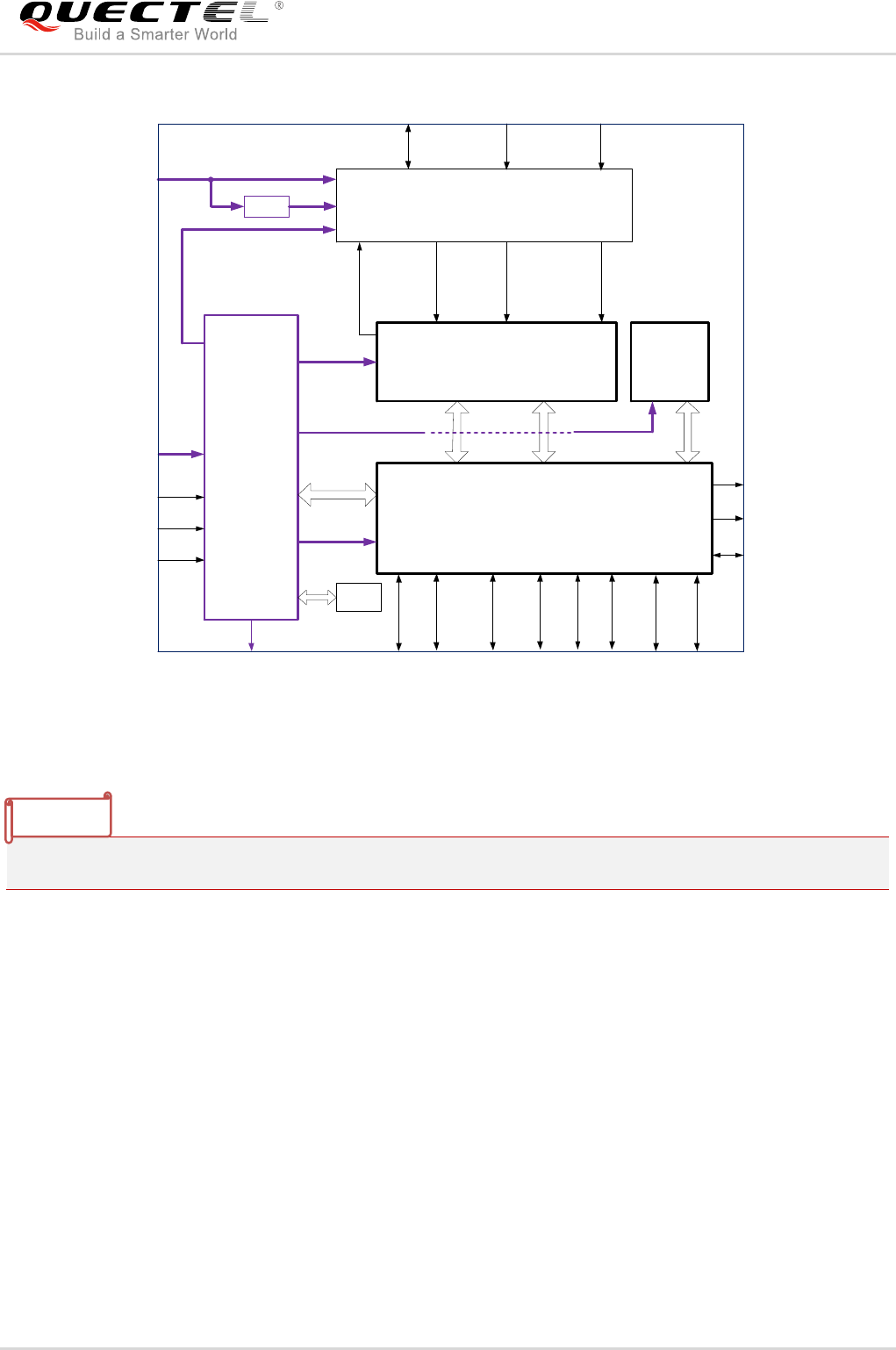
2.3. Functional Diagram
The following figure shows a block diagram of EG06 and illustrates the major functional parts.
Power management
Baseband
DDR+NAND flash
Radio frequency
Peripheral interfaces
PCIe Interface*
Comply with PCI Express Specification Revision 2.1
Used for Ethernet or WLAN communication
Rx-diversity
Support LTE/WCDMA Rx-diversity
GNSS Features
Gen8C-Lite of Qualcomm
Protocol: NMEA 0183
AT Commands
Compliant with 3GPP TS 27.007, 27.005 and Quectel enhanced AT
commands
Network Indication
Two pins including NET_MODE and NET_STATUS to indicate network
connectivity status
Antenna Interface
Including main antenna interface (ANT_MAIN), Rx-diversity antenna
interface (ANT_DIV) and GNSS antenna interface (ANT_GNSS)
Physical Characteristics
Size: (37.0±0.15)mm × (39.5±0.15)mm × (2.8±0.2)mm
Weight: approx. 6.7g
Temperature Range
Operation temperature range: -35°C ~ +75°C1)
Extended temperature range: -40°C ~ +85°C2)
Storage temperature range: -40°C ~ +90°C
Firmware Upgrade
USB2.0 interface and DFOTA*
RoHS
All hardware components are fully compliant with EU RoHS directive
NOTES
LTE-A Module Series
EG06 Hardware Design
EG06_Hardware_Design 17 / 89
Baseband
PMIC
Transceiver NAND
DDR2
SDRAM
Tx/Rx Blocks
ANT_MAIN ANT_DIVANT_GNSS
VBAT_BB
VBAT_RF
APT
PWRKEY
ADCs
VDD_EXT USB2.0/3.0 USIM PCM UART
I2C
RESET_N
19.2M
XO
STATUS
GPIOs
Control
IQ Control
Tx
PRx DRx
PCIe*
CLK_OUT
SD
SPI
Figure 1: Functional Diagram
“*” means under development.
2.4. Evaluation Board
In order to help customers develop applications with EG06, Quectel supplies an evaluation board (EVB),
USB to RS-232 converter cable, earphone, antenna and other peripherals to control or test the module.
NOTE
LTE-A Module Series
EG06 Hardware Design
EG06_Hardware_Design 18 / 89
3 Application Interface
3.1. General Description
EG06 is equipped with 299-pin LGA pads that can be connected to cellular application platform.
Sub-interfaces included in these pads are described in detail in the following chapters:
Power supply
(U)SIM interface
USB interface
UART interfaces
PCM and I2C interfaces
ADC interfaces
Network status indication
PCIe interface*
WLAN control interface*
SD card interface
USB_BOOT interface
“*” means under development.
NOTE
LTE-A Module Series
EG06 Hardware Design
EG06_Hardware_Design 19 / 89
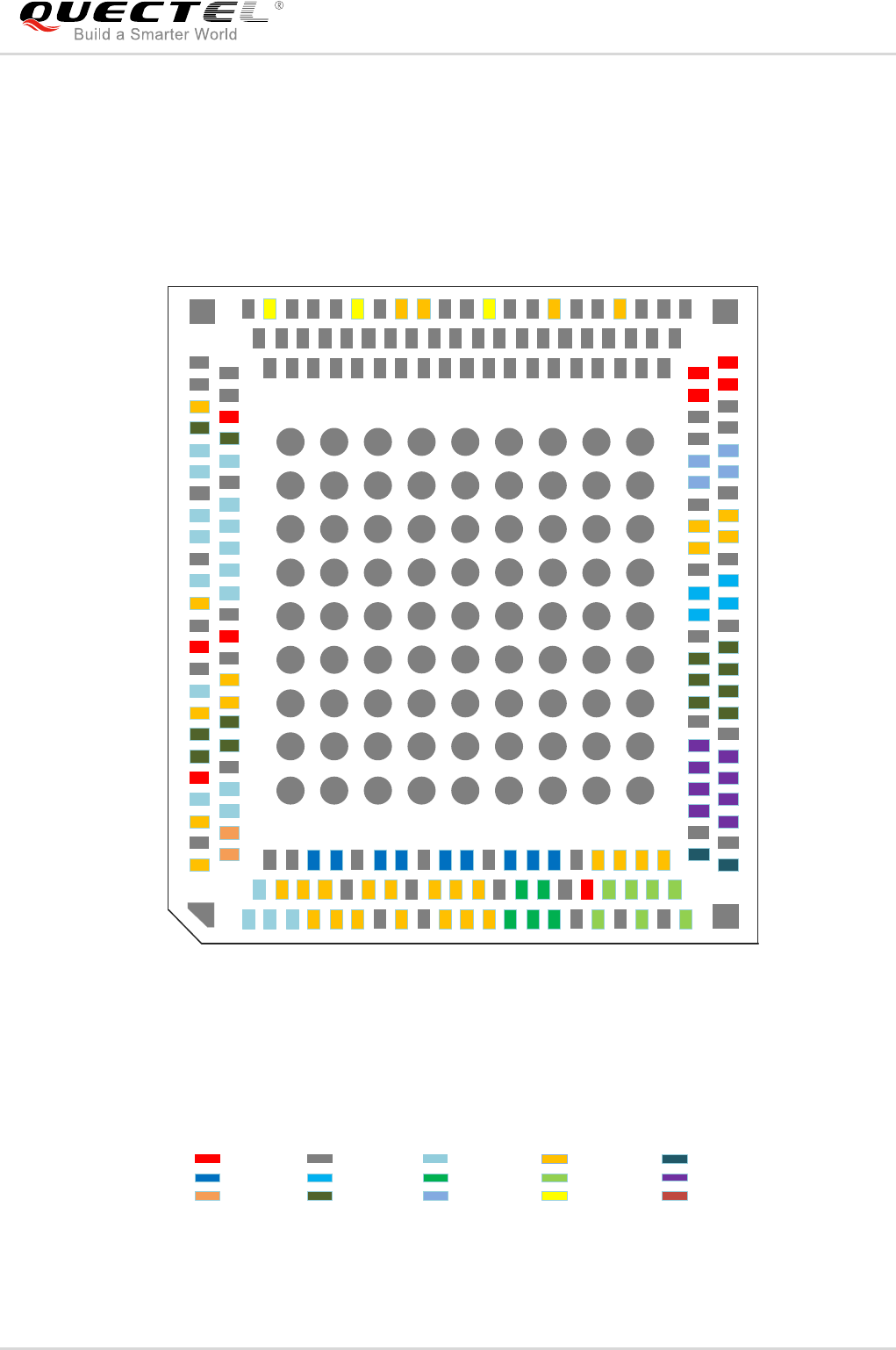
3.2. Pin Assignment
The following figure shows the pin assignment of EG06 module.
299
176
298
174
172
170
168
166
164
162
160
158
156
154
152
150
148
146
144
142
140
138
136
134
132
130
175
173
171
169
167
165
163
161
159
157
155
153
151
149
147
145
143
141
139
137
135
133
131
129
127
125
123
121
119
117
115
111
109
107
105
103
101
99
97
95
128
113
126
124
122
120
118
116
114
112
110
108
106
104
102
100
98
96
214
213
212
211
210
209
208
207
206
205
204
203
202
201
200
199
198
93
91
89
94
92
90
197
196
43
45
47
49
51
53
55
57
59
61
63
65
67
69
71
73
75
77
79
81
83
85
87
42
44
46
48
50
52
54
56
58
60
62
64
66
68
70
72
74
76
78
80
82
84
86
88
41
39
37
35
33
31
29
27
23
21
19
17
15
13
11
9
7
40
25
38
36
34
32
30
28
26
24
22
20
18
16
14
12
10
8
195
194
193
192
191
190
189
188
187
186
185
184
183
182
181
180
179
5
3
1
6
4
2
178
177
Power Pins GND Pins GPIO and Other Pins RESVRVED Pins
297
296
216 217 218215 219 220 221 222 223
224
233
242
251
260
269
278
287
225
234
243
252
261
270
279
288
226
235
244
253
262
271
280
289
227
236
272
281
290
228
237
273
282
291
229
238
274
283
292
230
239
248
257
266
275
284
293
231
240
249
258
267
276
285
294
232
241
250
259
268
277
286
295
PCIe Pins PCM Pins USIM Pins USB Pins
IIC Pins
SD Pins
ADC Pins UART Pins SPI Pins ANT Pins CLK Pins
RESET_N
PWRKEY
BT_EN
PM_ENABLE
USIM_PRESENCE
USIM_CLK
USIM_DATA
USIM_VDD
USIM_RST
USB_VBUS
USB_DM
USB_DP
USB_ID
USB_SS_TX_M
USB_SS_TX_P
USB_SS_RX_P
USB_SS_RX_M
I2C_SDA
I2C_SCL
SD_VDD
SD_DATA2
SD_DATA3
SD_DATA0
SD_DATA1
SD_CMD
SD_DETECT
SD_CLK
CTS
RTS RXD
DCD TXD
RI DTR
PCM_SYNC
PCM_CLK
PCM_IN
PCM_OUT
SPI_MOSI
SPI_CS
SPI_MISO
SPI_CLK
VBAT_RF
VBAT_RF
VBAT_RF
VBAT_RF
ANT_MAIN
ANT_GNSS
ANT_DIV
RESERVED
DBG_RXD
GPIO1
USB_BOOT
VDD_P2
DBG_TXD
GPIO2
OTG_PWR_EN
COEX_UART_TX
NET_MODE
WLAN_EN
W_DISABLE#
SLEEP_IND
COEX_UART_RX
WAKEUP_IN
RESERVED
VBAT_BB
VBAT_BB
WAKE_ON_WIRELESS
BT_TXD
BT_RXD
BT_CTS
BT_RTS
VDD_EXT WLAN_SLP_CLK
GND
NET_STATUS
STATUS
ADC0
ADC1
GND
GND GND
GND
GND
GND
GND
GND
GND
GND
GND
GND
PCIE_REFCLK_P
PCIE_REFCLK_M
PCIE_TX_M
PCIE_TX_P
PCIE_RX_M
PCIE_RX_P
PCIE_CLK_REQ_N
PCIE_RST_N
PCIE_WAKE_N
GND
GND
GND GND
GND
GND
GND
GND
GND
GND
GND GND
GND GND
USIM_GND
245 246 247
254 255 256
263 264 265
RESERVED
RESERVED
RESERVED
RESERVED
RESERVED
RESERVED
RESERVED
RESERVED RESERVED
RESERVED GND
RESERVED
GND RESERVED
RESERVED
GND
RESERVED
RESERVED
RESERVED
GND
GND
GND
GND
RESERVED
RESERVED
RESERVED
GND
RESERVED
GND
GND
GND
GND
GND
GND
RESERVED
RESERVED
RESERVED
RESERVED
RESERVED
RESERVED
RESERVED
RESERVED
RESERVED
RESERVED
RESERVED
RESERVED
Figure 2: Pin Assignment (Top View)
LTE-A Module Series
EG06 Hardware Design
EG06_Hardware_Design 20 / 89
1. Keep all RESERVED pins and unused pins unconnected.
2. GND pads 215~299 should be connected to ground in the design.
3.3. Pin Description
The following tables show the pin definition and description of EG06 module.
Table 3: I/O Parameters Definition
Type
Description
IO
Bidirectional
DI
Digital input
DO
Digital output
PI
Power input
PO
Power output
AI
Analog input
AO
Analog output
OD
Open drain
Table 4: Pin Description
Power Supply
Pin Name
Pin No.
I/O
Description
DC Characteristics
Comment
VBAT_BB
155,156
PI
Power supply for
the module’s
baseband part.
Vmax=4.3V
Vmin=3.3V
Vnorm=3.8V
It must be able to
provide sufficient
current up to 0.8A.
VBAT_RF
85, 86,
87, 88
PI
Power supply for
the module’s RF
part.
Vmax=4.3V
Vmin=3.3V
Vnorm=3.8V
It must be able to
provide sufficient
current up to 1.8A in a
transmitting burst.
NOTES

LTE-A Module Series
EG06 Hardware Design
EG06_Hardware_Design 21 / 89
VDD_EXT
168
PO
Provide 1.8V for
external circuit.
Vnorm=1.8V
IOmax=50mA
Power supply for
external GPIO’s pull up
circuits.
VDD_P2
135
PI
It is determined by
external circuit.
If an SD card is used,
connect VDD_P2 to
SD_VDD.
If an eMMC* is used,
connect VDD_P2 to
VDD_EXT.
GND
10, 13, 16,
17, 24, 30,
31, 35, 39,
44, 45, 54,
55, 63, 64,
69, 70, 75,
76, 81~84,
89~94,
96~100,
102~106,
108~112,
114, 116,
117, 118,
120~126,
128~133,
141, 142,
148, 153,
154, 157,
158, 167,
174, 177,
178, 181,
184, 187,
191,
196~299
Ground
Turn on/off
Pin Name
Pin No.
I/O
Description
DC Characteristics
Comment
PWRKEY
2
DI
Turn on/off the
module.
VIHmax=2.1V
VIHmin=1.3V
VILmax=0.5V
The output voltage is
0.8V because it is
pulled up to an
internal voltage
(800mV).
RESET_N
1
DI
Reset the module
VIHmax=2.1V
VIHmin=1.3V
VILmax=0.5V

LTE-A Module Series
EG06 Hardware Design
EG06_Hardware_Design 22 / 89
Status Indication
Pin Name
Pin No.
I/O
Description
DC Characteristics
Comment
STATUS
171
DO
Indicate the
module’s operation
status.
VOHmin=1.35V
VOLmax=0.45V
1.8V power domain.
If unused, keep it
open.
NET_MODE
147
DO
Indicate the
module’s network
registration mode
VOHmin=1.35V
VOLmax=0.45V
1.8V power domain.
If unused, keep it
open.
NET_
STATUS
170
DO
Indicate the
module’s network
activity status
VOHmin=1.35V
VOLmax=0.45V
1.8V power domain.
If unused, keep it
open.
USB Interface
Pin Name
Pin No.
I/O
Description
DC Characteristics
Comment
USB_VBUS
32
PI
USB connection
detection
Vmax=5.25V
Vmin=3.0V
Vnorm=5.0V
USB_DP
34
IO
USB 2.0 differential
data bus - plus
Compliant with USB
2.0 standard
specifications.
Require differential
impedance of 90Ω.
USB_DM
33
IO
USB 2.0 differential
data bus - minus
Compliant with USB
2.0 standard
specifications.
USB_ID
36
DI
OTG identification
VILmin=-0.3V
VILmax=0.6V
VIHmin=1.2V
VIHmax=2.0V
1.8V power domain.
If unused, keep it
open.
USB_SS_
TX_P
38
AO
USB 3.0 super
speed
transmission- plus
Compliant with USB
3.0 standard
specifications.
Require differential
impedance of 90Ω.
USB_SS_
TX_M
37
AO
USB 3.0 super
speed
transmission-
minus
USB_SS_
RX_P
40
AI
USB 3.0 super
speed receiving-
plus
Require differential
impedance of 90Ω.
USB_SS_
RX_M
41
AI
USB 3.0
super-speed
receiving- minus

LTE-A Module Series
EG06 Hardware Design
EG06_Hardware_Design 23 / 89
OTG_PWR_
EN
143
DO
OTG power control
VOLmax=0.45V
VOHmin=1.35V
(U)SIM Interface
Pin Name
Pin No.
I/O
Description
DC Characteristics
Comment
USIM_GND
24
Specified ground
for (U)SIM card
USIM_VDD
26
PO
Power supply for
(U)SIM card
For 1.8V (U)SIM:
Vmax=1.9V
Vmin=1.7V
For 3.0V (U)SIM:
Vmax=3.05V
Vmin=2.75V
IOmax=50mA
Either 1.8V or 3.0V is
supported by the
module
automatically.
USIM_
DATA
29
IO
Data signal of
(U)SIM card
For 1.8V (U)SIM:
VILmax=0.36V
VIHmin=1.26V
VOLmax=0.4V
VOHmin=1.45V
For 3.0V (U)SIM:
VILmax=0.57V
VIHmin=2.0V
VOLmax=0.4V
VOHmin=2.3V
USIM_CLK
27
DO
Clock signal of
(U)SIM card
For 1.8V (U)SIM:
VOLmax=0.4V
VOHmin=1.45V
For 3.0V (U)SIM:
VOLmax=0.4V
VOHmin=2.3V
USIM_RST
28
DO
Reset signal of
(U)SIM card
For 1.8V (U)SIM:
VOLmax=0.4V
VOHmin=1.45V
For 3.0V (U)SIM:
VOLmax=0.4V
VOHmin=2.3V
USIM_
PRESENCE
25
DI
(U)SIM card
insertion detection
VILmin=-0.3V
VILmax=0.6V
VIHmin=1.2V
VIHmax=2.0V
1.8V power domain.
If unused, keep it
open.

LTE-A Module Series
EG06 Hardware Design
EG06_Hardware_Design 24 / 89
UART Interface
Pin Name
Pin No.
I/O
Description
DC Characteristics
Comment
RI
61
DO
Ring indicator
VOLmax=0.45V
VOHmin=1.35V
1.8V power domain.
If unused, keep it
open.
DCD
59
DO
Data carrier
detection
VOLmax=0.45V
VOHmin=1.35V
1.8V power domain.
If unused, keep it
open.
CTS
56
DO
Clear to send
VOLmax=0.45V
VOHmin=1.35V
1.8V power domain.
If unused, keep it
open.
RTS
57
DI
Request to send
VILmin=-0.3V
VILmax=0.6V
VIHmin=1.2V
VIHmax=2.0V
1.8V power domain.
If unused, keep it
open.
DTR
62
DI
Data terminal
ready, sleep mode
control
VILmin=-0.3V
VILmax=0.6V
VIHmin=1.2V
VIHmax=2.0V
1.8V power domain.
Pull-up by default.
Pulling down to low
level will wake up the
module.
If unused, keep it
open.
TXD
60
DO
Transmit data
VOLmax=0.45V
VOHmin=1.35V
1.8V power domain.
If unused, keep it
open.
RXD
58
DI
Receive data
VILmin=-0.3V
VILmax=0.6V
VIHmin=1.2V
VIHmax=2.0V
1.8V power domain.
If unused, keep it
open.
BT Interface
Pin Name
Pin No.
I/O
Description
DC Characteristics
Comment
BT_TXD
163
DO
Transmit data
VOLmax=0.45V
VOHmin=1.35V
1.8V power domain.
If unused, keep it
open.
BT_RXD
165
DI
Receive data
VILmin=-0.3V
VILmax=0.6V
VIHmin=1.2V
VIHmax=2.0V
1.8V power domain.
If unused, keep it
open.
BT_RTS
166
DI
Request to send
VILmin=-0.3V
VILmax=0.6V
VIHmin=1.2V
1.8V power domain.
If unused, keep it
open.
LTE-A Module Series
EG06 Hardware Design
EG06_Hardware_Design 25 / 89
VIHmax=2.0V
BT_CTS
164
DO
Clear to send
VOLmax=0.45V
VOHmin=1.35V
1.8V power domain.
If unused, keep it
open.
BT_EN*
3
DO
BT function
enabled
VOLmax=0.45V
VOHmin=1.35V
1.8V power domain.
Keep it open.
This function is under
development
Debug UART Interface
Pin Name
Pin No.
I/O
Description
DC Characteristics
Comment
DBG_RXD
136
DI
Receive data
VILmin=-0.3V
VILmax=0.6V
VIHmin=1.2V
VIHmax=2.0V
1.8V power domain.
If unused, keep it
open.
DBG_TXD
137
DO
Transmit data
VOLmax=0.45V
VOHmin=1.35V
1.8V power domain.
If unused, keep it
open.
ADC Interface
Pin Name
Pin No.
I/O
Description
DC Characteristics
Comment
ADC0
173
AI
General purpose
analog to digital
converter interface
Voltage range:
0.15V to VBAT_BB
If unused, keep it
open.
ADC1
175
AI
General purpose
analog to digital
converter interface
Voltage range:
0.15V to VBAT_BB
If unused, keep it
open.
PCM and I2C Interface
Pin Name
Pin No.
I/O
Description
DC Characteristics
Comment
PCM_IN
66
DI
PCM data input
VILmin=-0.3V
VILmax=0.6V
VIHmin=1.2V
VIHmax=2.0V
1.8V power domain.
If unused, keep it
open.
PCM_OUT
68
DO
PCM data output
VOLmax=0.45V
VOHmin=1.35V
1.8V power domain.
If unused, keep it
open.
PCM_SYNC
65
IO
PCM data frame
synchronization
signal
VOLmax=0.45V
VOHmin=1.35V
VILmin=-0.3V
VILmax=0.6V
VIHmin=1.2V
1.8V power domain.
In master mode, it is
an output signal. In
slave mode, it is an
input signal.
If unused, keep it
open.
LTE-A Module Series
EG06 Hardware Design
EG06_Hardware_Design 26 / 89
VIHmax=2.0V
PCM_CLK
67
IO
PCM clock
VOLmax=0.45V
VOHmin=1.35V
VILmin=-0.3V
VILmax=0.6V
VIHmin=1.2V
VIHmax=2.0V
1.8V power domain.
In master mode, it is
an output signal. In
slave mode, it is an
input signal.
If unused, keep it
open.
I2C_SCL
43
OD
I2C serial clock
Used for external
codec.
1.8V power domain.
An external pull-up
resistor is required.
1.8V only. If unused,
keep it open.
I2C_SDA
42
OD
I2C serial data
Used for external
codec.
1.8V power domain.
An external pull-up
resistor is required.
1.8V only. If unused,
keep it open.
SPI Interface
Pin Name
Pin No.
I/O
Description
DC Characteristics
Comment
SPI_CS
79
DO
Chip select of SPI
interface
VOLmax=0.45V
VOHmin=1.35V
1.8V power domain.
If unused, keep it
open.
SPI_CLK
80
DO
Clock signal of SPI
interface
VOLmax=0.45V
VOHmin=1.35V
1.8V power domain.
If unused, keep it
open.
SPI_MOSI
77
DO
Master output
slave input of SPI
interface
VOLmax=0.45V
VOHmin=1.35V
1.8V power domain.
If unused, keep it
open.
SPI_MISO
78
DI
Master input
slave output of SPI
interface
VILmin=-0.3V
VILmax=0.6V
VIHmin=1.2V
VIHmax=2.0V
1.8V power domain.
If unused, keep it
open.
PCIe Interface*
Pin Name
Pin No.
I/O
Description
DC Characteristics
Comment
PCIE_REF
CLK_P
179
AO
Output PCIe
reference clock -
plus
If unused, keep it
open.
PCIE_REF
CLK_M
180
AO
Output PCIe
reference clock -
minus
If unused, keep it
open.
PCIE_TX_M
182
AO
PCIe transmission
- minus
If unused, keep it
open.

LTE-A Module Series
EG06 Hardware Design
EG06_Hardware_Design 27 / 89
PCIE_TX_P
183
AO
PCIe transmission
- plus
If unused, keep it
open.
PCIE_RX_M
185
AI
PCIe receiving-
minus
If unused, keep it
open.
PCIE_RX_P
186
AI
PCIe receiving -
plus
If unused, keep it
open.
PCIE_CLK_
REQ_N
188
IO
PCIe clock request
VOLmax=0.45V
VOHmin=1.35V
VILmin=-0.3V
VILmax=0.6V
VIHmin=1.2V
VIHmax=2.0V
In master mode, it is
an input signal.
In slave mode, it is an
output signal.
If unused, keep it
open.
PCIE_RST_N
189
IO
PCIe reset
VOLmax=0.45V
VOHmin=1.35V
VILmin=-0.3V
VILmax=0.6V
VIHmin=1.2V
VIHmax=2.0V
In master mode, it is
an output signal.
In slave mode, it is an
input signal.
If unused, keep it
open.
PCIE_WAKE_
N
190
IO
PCIe wake
VOLmax=0.45V
VOHmin=1.35V
VILmin=-0.3V
VILmax=0.6V
VIHmin=1.2V
VIHmax=2.0V
VIHmax=2.0V
In master mode, it is
an input signal.
In slave mode, it is an
output signal.
If unused, keep it
open.
WLAN Control Interface*
Pin Name
Pin No.
I/O
Description
DC Characteristics
Comment
PM_ENABLE
5
DO
Enable WLAN
power
VOLmax=0.45V
VOHmin=1.35V
1.8V power domain.
If unused, keep it
open.
WAKE_ON_
WIRELESS
160
DI
Wake up the host
(EG06 module) by
Wi-Fi module.
VILmin=-0.3V
VILmax=0.6V
VIHmin=1.2V
VIHmax=2.0V
1.8V power domain.
Active low.
If unused, keep it
open.
WLAN_EN
149
DO
WLAN function
enable control
VOLmax=0.45V
VOHmin=1.35V
1.8V power domain.
Active high.
If unused, keep it
open.
COEX_UART_
RX
146
DI
LTE/WLAN
coexistence signal
VILmin=-0.3V
VILmax=0.6V
VIHmin=1.2V
VIHmax=2.0V
1.8V power domain.
If unused, keep it
open.

LTE-A Module Series
EG06 Hardware Design
EG06_Hardware_Design 28 / 89
COEX_UART_
TX
145
DO
LTE/WLAN
coexistence signal
VOLmax=0.45V
VOHmin=1.35V
1.8V power domain.
If unused, keep it
open.
WLAN_SLP_
CLK
169
DO
WLAN sleep clock
VOLmax=0.45V
VOHmin=1.35V
If unused, keep it
open.
SD Card Interface
Pin Name
Pin No.
I/O
Description
DC Characteristics
Comment
SD_VDD
46
PO
Power supply for
pull up voltage of
SD card bus
For 1.8V SD:
Vmax=1.9V
Vmin=1.75V
For 3.0V SD:
Vmax=3.05V
Vmin=2.75V
IOmax=50mA
Either 1.8V or 3.0V is
supported by the
module
automatically.
Power supply of SD
card must be
provided by an
external power
supply.
SD_DATA0
49
IO
Secure digital
controller data bit 0
For1.8V SD:
VOLmax=0.45V
VOHmin=1.4V
VILmin=-0.3V
VILmax=0.58V
VIHmin=1.3V
VIHmax=2.0V
For 3.0V SD:
VOLmax=0.35V
VOHmin=2.15V
VILmin=-0.3V
VILmax=0.7V
VIHmin=1.8V
VIHmax=3.15V
If unused, keep it
open.
SD_DATA1
50
IO
Secure digital
controller data bit 1
If unused, keep it
open.
SD_DATA2
47
IO
Secure digital
controller data bit 2
If unused, keep it
open.
SD_DATA3
48
IO
Secure digital
controller data bit 3
If unused, keep it
open.
SD_CMD
51
DO
Command signal
for SD card
If unused, keep it
open.
SD_CLK
53
DO
Serial clock signal
for SD card
If unused, keep it
open.
SD_ DETECT
52
DI
SD card insertion
detection
VILmin=-0.3V
VILmax=0.6V
VIHmin=1.2V
VIHmax=2.0V
If unused, keep it
open.
RF Interface
Pin Name
Pin No.
I/O
Description
DC Characteristics
Comment
ANT_DIV
127
AI
Diversity antenna
interface
50Ω impedance.
If unused, keep it
open.

LTE-A Module Series
EG06 Hardware Design
EG06_Hardware_Design 29 / 89
ANT_MAIN
107
IO
Main antenna
interface
50Ω impedance.
ANT_GNSS
119
AI
GNSS antenna
interface
50Ω impedance.
If unused, keep it
open.
GPIO Pins
Pin Name
Pin No.
I/O
Description
DC Characteristics
Comment
WAKEUP_IN
150
DI
Sleep mode control
VILmin=-0.3V
VILmax=0.6V
VIHmin=1.2V
VIHmax=2.0V
1.8V power domain.
Pull-up by default.
Low level wakes up
the module.
If unused, keep it
open.
W_DISABLE#
151
DI
Airplane mode
control
VILmin=-0.3V
VILmax=0.6V
VIHmin=1.2V
VIHmax=2.0V
1.8V power domain.
Pull-up by default.
In low voltage level,
the module can enter
into airplane mode.
If unused, keep it
open.
GPIO1
138
IO
General purpose
input/output port
VOLmax=0.45V
VOHmin=1.35V
VILmin=-0.3V
VILmax=0.6V
VIHmin=1.2V
VIHmax=2.0V
If unused, keep it
open.
GPIO2
139
IO
Other Pins
Pin Name
Pin No.
I/O
Description
DC Characteristics
Comment
USB_BOOT
140
DI
Force the module
to enter into
emergency
download mode
VILmin=-0.3V
VILmax=0.6V
VIHmin=1.2V
VIHmax=2.0V
1.8V power domain.
If unused, keep it
open.
SLEEP_IND
144
DO
Sleep instruction
VOLmax=0.45V
VOHmin=1.35V
1.8V power domain.
If unused, keep it
open.
RESERVED Pins
Pin Name
Pin No.
I/O
Description
DC Characteristics
Comment
RESERVED
4, 6, 7, 8,
9, 11, 12,
Reserved
Keep these pins
unconnected.

LTE-A Module Series
EG06 Hardware Design
EG06_Hardware_Design 30 / 89
RESERVED
14, 15,
18~23,
71~74, 95,
101, 113,
115, 134,
152, 159,
161, 162,
172, 176,
192~195
Reserved
Keep these pins
unconnected.
3.4. Operating Modes
The table below briefly summarizes the various operating modes referred in the following chapters.
Table 5: Overview of Operating Modes
Mode
Details
Normal
Operation
Idle
Software is active. The module has registered on the network, and it is
ready to send and receive data.
Talk/Data
Network connection is ongoing. In this mode, the power consumption is
decided by network setting and data transfer rate.
Minimum
Functionality
Mode
AT+CFUN command can set the module to a minimum functionality mode without
removing the power supply. In this case, both RF function and (U)SIM card will be
invalid.
Airplane Mode
AT+CFUN command or W_DISABLE# pin can set the module to airplane mode. In
this case, RF function will be invalid.
Sleep Mode
In this mode, the current consumption of the module will be reduced to the minimal
level. During this mode, the module can still receive paging message, SMS, voice
call and TCP/UDP data from the network normally.
Power Down
Mode
In this mode, the power management unit shuts down the power supply. Software is
not active. The serial interfaces are not accessible. Operating voltage (connected to
VBAT_RF and VBAT_BB) remains applied.
LTE-A Module Series
EG06 Hardware Design
EG06_Hardware_Design 31 / 89
3.5. Power Saving
3.5.1. Sleep Mode
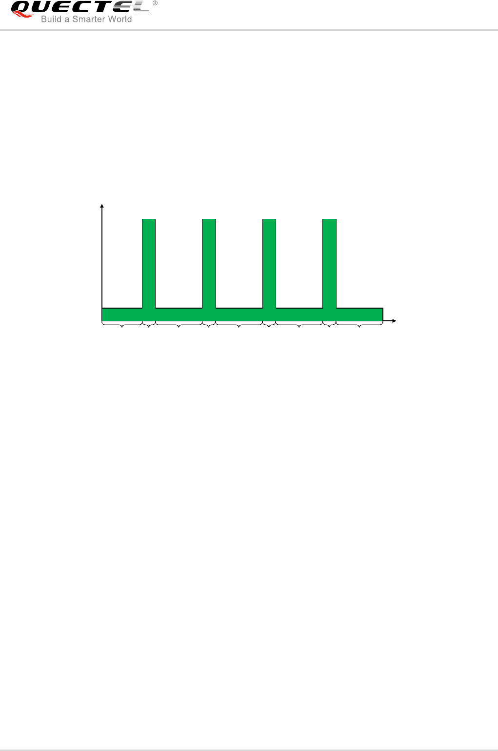
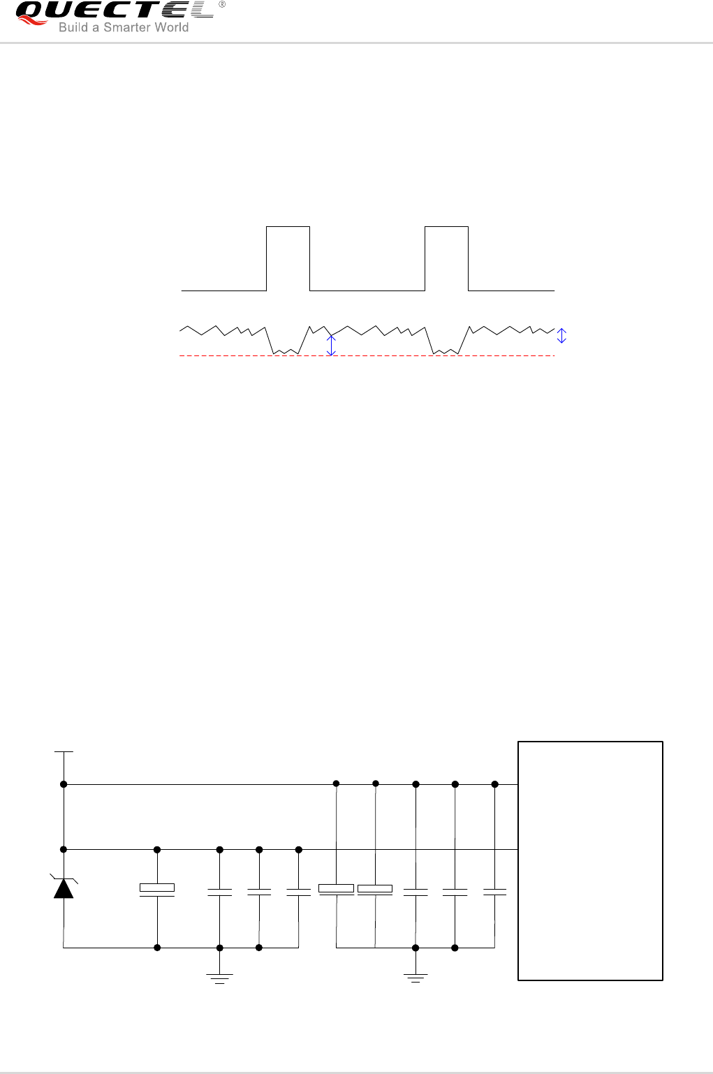
DRX on EG06 is able to reduce the current consumption to a minimum value during the sleep mode, and
DRX cycle index values are broadcasted by the wireless network. The figure below shows the relationship
between the DRX run time and the current consumption in sleep mode. The longer the DRX runs, the
lower the current consumption will be.
Current Consumption
Run Time
DRX OFF ON OFF ON OFF ON OFF ON OFF
Figure 3: DRX Run Time and Current Consumption in Sleep Mode
The following section describes power saving procedure of EG06 module.
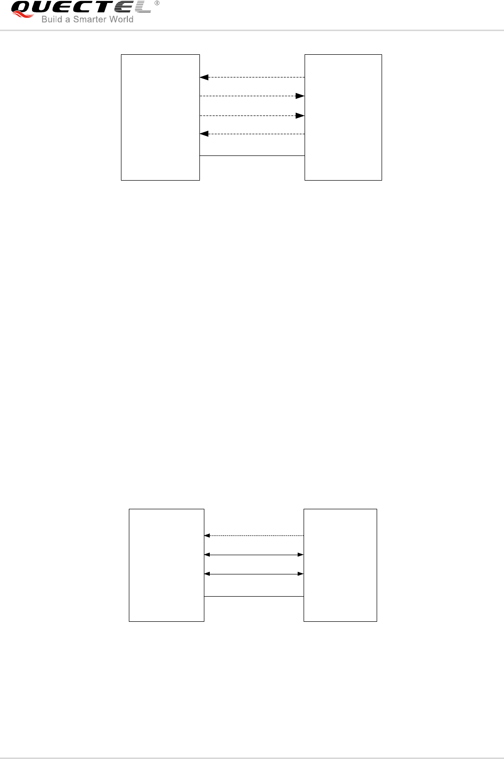
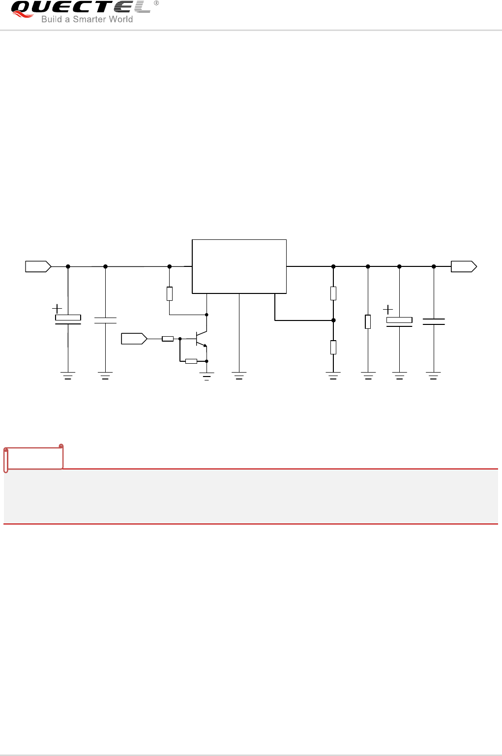
3.5.1.1. UART Application
If the host communicates with the module via UART interface, the following preconditions can let the
module enter into sleep mode.
Execute AT+QSCLK=1 command to enable sleep mode.
Drive DTR to high level.
The following figure shows the connection between the module and the host.
LTE-A Module Series
EG06 Hardware Design
EG06_Hardware_Design 32 / 89
RXD
TXD
RI
DTR
TXD
RXD
EINT
GPIO
Module Host
GND GND
Figure 4: Sleep Mode Application via UART
Driving the host DTR to low level will wake up the module.
When EG06 has a URC to report, RI signal will wake up the host. Please refer to Chapter 3.16 for
details about RI behavior.
3.5.1.2. USB Application with USB Remote Wakeup Function
If the host supports USB suspend/resume and remote wakeup function, the following three preconditions
must be met to let the module enter into the sleep mode.
Execute AT+QSCLK=1 command to enable the sleep mode.
Ensure the DTR is held at high level or keep it open.
The host’s USB bus, which is connected with the module’s USB interface, enters into suspended
state.
The following figure shows the connection between the module and the host.
USB_VBUS
USB_DP
USB_DM
VDD
USB_DP
USB_DM
Module Host
GND GND
Figure 5: Sleep Mode Application with USB Remote Wakeup
Sending data to EG06 through USB will wake up the module.
When EG06 has a URC to report, the module will send remote wake-up signals to USB bus so as to
wake up the host.
LTE-A Module Series
EG06 Hardware Design
EG06_Hardware_Design 33 / 89
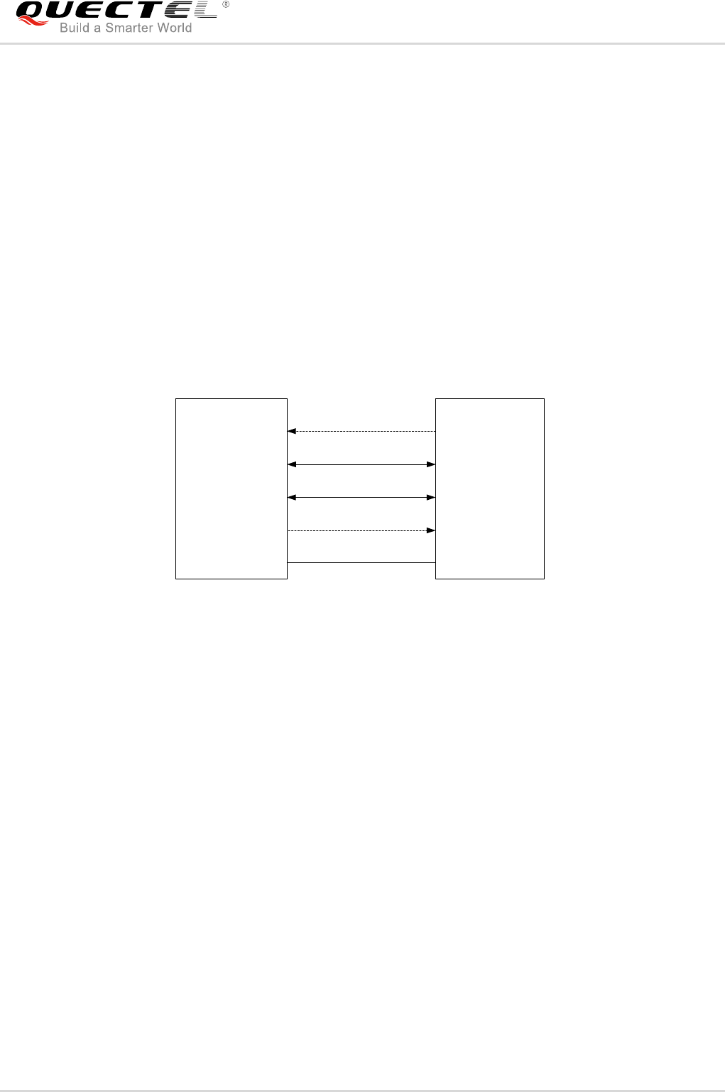
3.5.1.3. USB Application with USB Suspend/Resume and RI Function
If the host supports USB suspend/resume, but does not support remote wake-up function, the RI signal is
needed to wake up the host.
There are three preconditions to let the module enter into the sleep mode.
Execute AT+QSCLK=1 command to enable the sleep mode.
Ensure the DTR is held at high level or keep it open.
The host’s USB bus, which is connected with the module’s USB interface, enters into suspended
state.
The following figure shows the connection between the module and the host.
USB_VBUS
USB_DP
USB_DM
VDD
USB_DP
USB_DM
Module Host
GND GND
RI EINT
Figure 6: Sleep Mode Application with RI
Sending data to EG06 through USB will wake up the module.
When EG06 has a URC to report, RI signal will wake up the host.
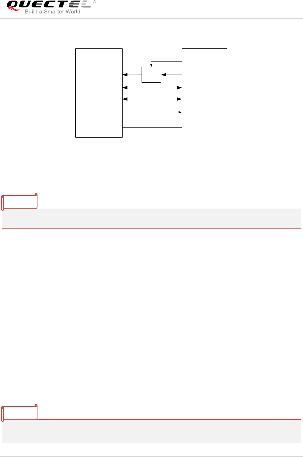
3.5.1.4. USB Application without USB Suspend Function
If the host does not support USB suspend function, USB_VBUS should be disconnected with an external
control circuit to let the module enter into sleep mode.
Execute AT+QSCLK=1 command to enable the sleep mode.
Ensure the DTR is held at high level or keep it open.
Disconnect USB_VBUS.
LTE-A Module Series
EG06 Hardware Design
EG06_Hardware_Design 34 / 89
The following figure shows the connection between the module and the host.
USB_VBUS
USB_DP
USB_DM
VDD
USB_DP
USB_DM
Module Host
RI EINT
Power
Switch
GPIO
GND GND
Figure 7: Sleep Mode Application without Suspend Function
Switching on the power switch to supply power to USB_VBUS will wake up the module.
Please pay attention to the level match shown in dotted line between the module and the host.
3.5.2. Airplane Mode
When the module enters into airplane mode, the RF function does not work, and all AT commands
correlative with RF function will be inaccessible. This mode can be set via the following ways.
Hardware:
The W_DISABLE# pin is pulled up by default; driving it to low level will let the module enter into airplane
mode.
Software:
AT+CFUN command provides the choice of the functionality level through setting <fun> into 0, 1 or 4.
AT+CFUN=0: Minimum functionality mode; both (U)SIM and RF functions are disabled.
AT+CFUN=1: Full functionality mode (by default).
AT+CFUN=4: Airplane mode. RF function is disabled.
1. The W_DISABLE# control function is disabled in firmware by default. It can be enabled by
AT+QCFG="airplanecontrol" command, and this command is under development.
NOTES
NOTE

LTE-A Module Series
EG06 Hardware Design
EG06_Hardware_Design 35 / 89
2. The execution of AT+CFUN command will not affect GNSS function.
3.6. Power Supply
3.6.1. Power Supply Pins
EG06 provides six VBAT pins dedicated to connect with the external power supply. There are two
separate voltage domains for VBAT.
Four VBAT_RF pins for module’s RF part
Two VBAT_BB pins for module’s baseband part
The following table shows the details of VBAT pins and ground pins.
Table 6: VBAT and GND Pins
Pin Name
Pin No.
Description
Min.
Typ.
Max.
Unit
VBAT_RF
85, 86
87, 88
Power supply for module’s
RF part
3.3
3.8
4.3
V
VBAT_BB
155, 156
Power supply for module’s
baseband part
3.3
3.8
4.3
V
GND
10, 13, 16, 17, 24,
30, 31, 35, 39, 44,
45, 54, 55, 63, 64,
69, 70, 75, 76,
81~84, 89~94,
96~100, 102~106,
108~112, 114,117,
118, 120~126,
128~133, 141,142,
148, 153, 154,157,
158, 167, 174, 177,
178, 181, 184, 187,
191, 217, 196~214,
224~299
Ground
-
0
-
V
LTE-A Module Series
EG06 Hardware Design
EG06_Hardware_Design 36 / 89
3.6.2. Decrease Voltage Drop
The power supply range of the module is from 3.3V to 4.3V. Please make sure the input voltage will never
drop below 3.3V. The following figure shows the voltage drop during Tx power in 3G and 4G networks.
VCC
Burst
Transmission
Min. 3.3V
Ripple
Drop
Burst
Transmission
Figure 8: Power Supply Limits during Tx Power
To decrease voltage drop, a bypass capacitor of about 100µF with low ESR should be used, and a
multi-layer ceramic chip (MLCC) capacitor array should also be reserved due to its ultra-low ESR. It is
recommended to use three ceramic capacitors (100nF, 33pF, 10pF) for composing the MLCC array, and
place these capacitors close to VBAT pins. The main power supply from an external application has to be
a single voltage source and can be expanded to two sub paths with star structure. The width of VBAT_BB
trace should be no less than 1mm; and the width of VBAT_RF trace should be no less than 2mm. In
principle, the longer the VBAT trace is, the wider it will be.
In addition, in order to get a stable power source, it is suggested that customers should use a zener diode
of which reverse zener voltage is 5.1V and dissipation power is more than 0.5W. The following figure
shows the star structure of the power supply.
Module
VBAT_RF
VBAT_BB
VBAT
C1
100uF
C7
100nF
C8
33pF
C9
10pF
+
+
C2
100nF
C5
100 uF
C3
33pF
C4
10pF
D1
5.1V
+
C6
100uF
Figure 9: Star Structure of the Power Supply
LTE-A Module Series
EG06 Hardware Design
EG06_Hardware_Design 37 / 89
3.6.3. Reference Design for Power Supply
Power design for the module is very important, as the performance of the module largely depends on the
power source. The power supply of EG06 should be able to provide sufficient current up to 2A at least. If
the voltage drop between the input and output is not too high, it is suggested that an LDO should be used
to supply power for the module. If there is a big voltage difference between the input source and the
desired output (VBAT), a buck converter is preferred to be used as the power supply.
The following figure shows a reference design for +5V input power source. The designed output of the
power supply is about 3.8V and the maximum load current is 3A.
DC_IN
MIC29302WU
IN OUT
EN
GND
ADJ
2 4
1
3
5
VBAT
100nF 470uF 100nF
100K
47K
470uF
470R
51K 1%
1%
4.7K
47K
VBAT_EN
Figure 10: Reference Circuit of Power Supply
In order to avoid damaging internal flash, please do not switch off the power supply when the module
works normally. Only after the module is shut down by PWRKEY or AT command, the power supply can
be cut off.
3.6.4. Monitor the Power Supply
AT+CBC command can be used to monitor the VBAT_BB voltage value. For more details, please refer to
document [1].
3.7. Turn on and off Scenarios
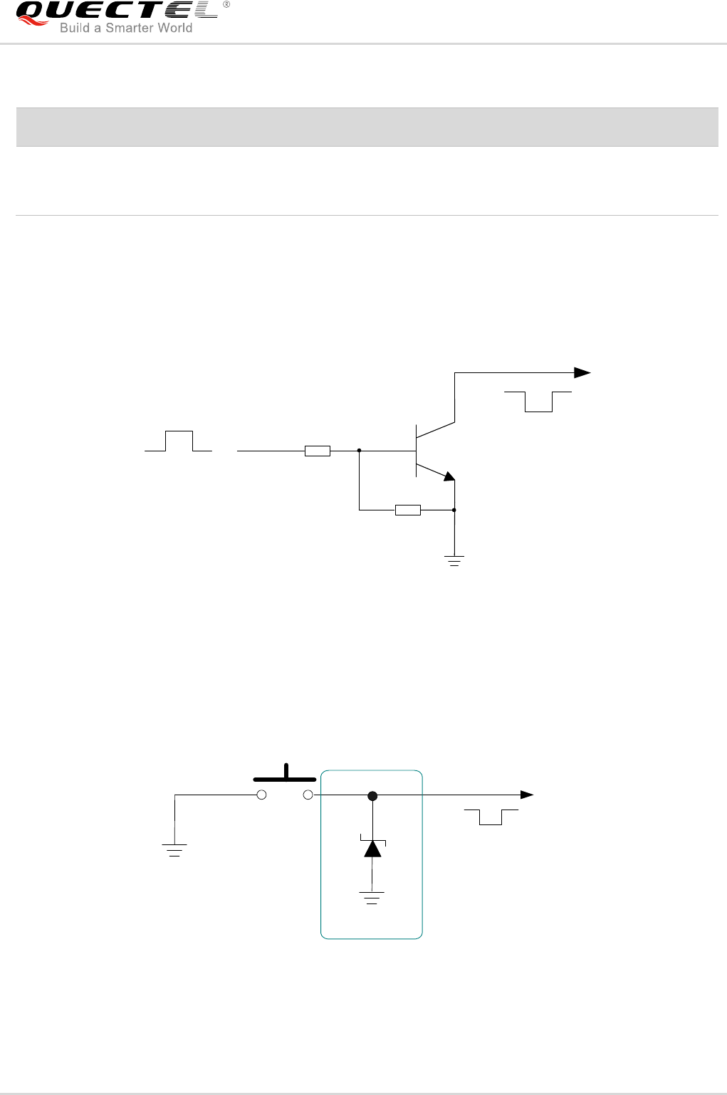
3.7.1. Turn on Module Using the PWRKEY
The following table shows the pin definition of PWRKEY.
NOTE
LTE-A Module Series
EG06 Hardware Design
EG06_Hardware_Design 38 / 89
Table 7: PWRKEY Pin Description
When EG06 is in power down mode, it can be turned on to normal mode by driving the PWRKEY pin to a
low level for at least 500ms. It is recommended to use an open drain/collector driver to control the
PWRKEY. After STATUS pin outputs a high level, PWRKEY pin can be released. A simple reference
circuit is illustrated in the following figure.
Turn on pulse
PWRKEY
4.7K
47K
≥500ms
Figure 11: Turn on the Module Using Driving Circuit
Another way to control the PWRKEY is using a button directly. When pressing the key, electrostatic strike
may generate from finger. Therefore, a TVS component is indispensable to be placed nearby the button
for ESD protection. A reference circuit is shown in the following figure.
PWRKEY
S1
Close to S1
TVS
Figure 12: Turn on the Module Using Keystroke
Pin Name
Pin No.
Description
DC Characteristics
Comment
PWRKEY
2
Turn on/off the module
VIHmax=2.1V
VIHmin=1.3V
VILmax=0.5V
The output voltage is 0.8V
because it is pulled up to an
internal voltage (800mV).
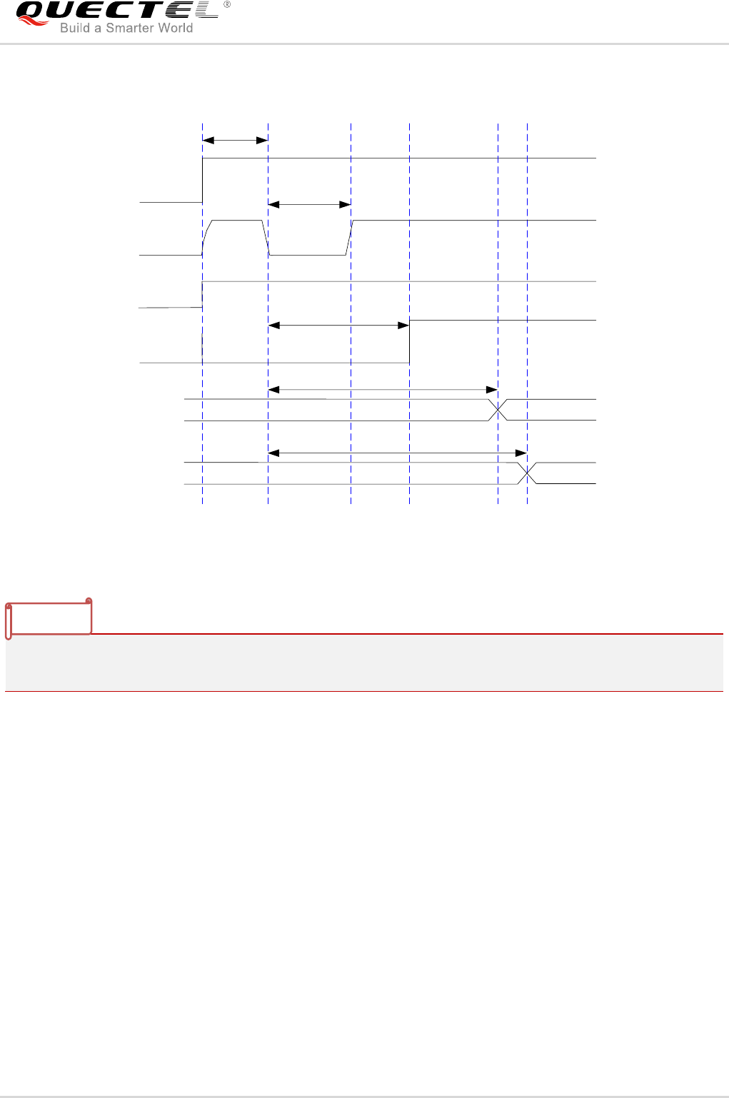
LTE-A Module Series
EG06 Hardware Design
EG06_Hardware_Design 39 / 89
The turn on scenario is illustrated in the following figure.
VIL≤0.5V
VIH≥1.3V
VBAT
PWRKEY
≥500ms
RESET_N
STATUS
Inactive Active
UART
NOTE
Inactive Active
USB
≥11.5s
≥13s
≥14s
Figure 13: Timing of Turning on Module
Please make sure that VBAT is stable before pulling down PWRKEY pin. The time between them is no
less than 30ms.
3.7.2. Turn off Module
The following procedures can be used to turn off the module:
Normal power down procedure: Turn off the module using the PWRKEY pin.
Normal power down procedure: Turn off the module using AT+QPOWD command.
3.7.2.1. Turn off Module Using the PWRKEY Pin
Driving the PWRKEY pin to a low level voltage for at least 800ms, the module will execute power-down
procedure after the PWRKEY is released. The power-down scenario is illustrated in the following figure.
NOTE
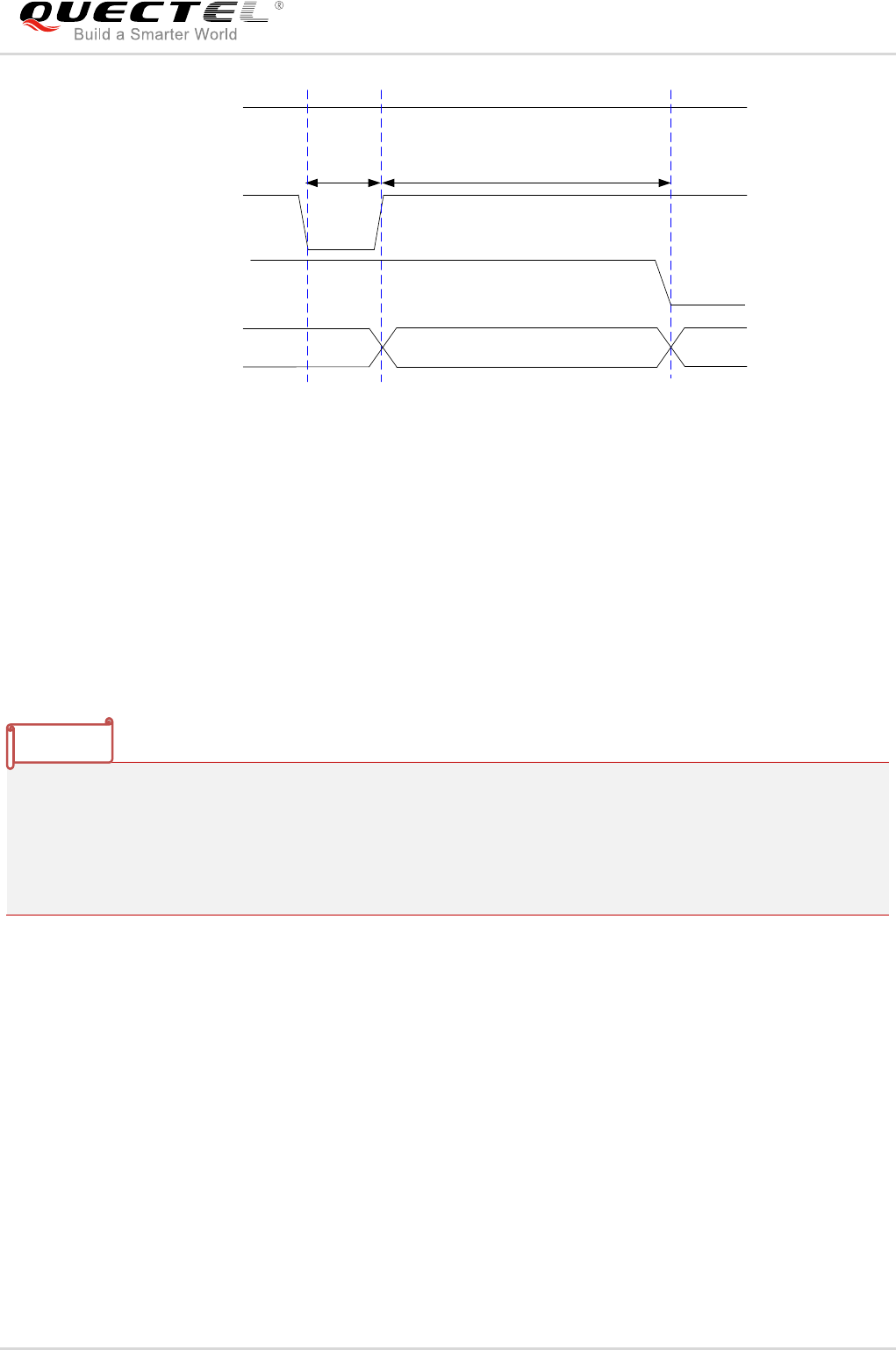
LTE-A Module Series
EG06 Hardware Design
EG06_Hardware_Design 40 / 89
VBAT
PWRKEY
≥800ms
RUNNING Power-down procedure OFF
Module
Status
STATUS
≥30s
Figure 14: Timing of Turning off Module
3.7.2.2. Turn off Module Using AT Command
It is also a safe way to use AT+QPOWD command to turn off the module, which is similar to turning off the
module via PWRKEY Pin.
Please refer to document [1] for details about AT+QPOWD command.
1. In order to avoid damaging internal flash, please do not switch off the power supply when the module
works normally. Only after the module is shut down by PWRKEY or AT command, the power supply
can be cut off.
2. When turn off module with AT command, please keep PWRKEY at high level after the execution of
power-off command. Otherwise the module will be turned on again after successfully turn-off.
3.8. Reset the Module
The RESET_N pin can be used to reset the module. The module can be reset by driving the RESET_N to
a low level voltage for 250ms~600ms.
NOTES
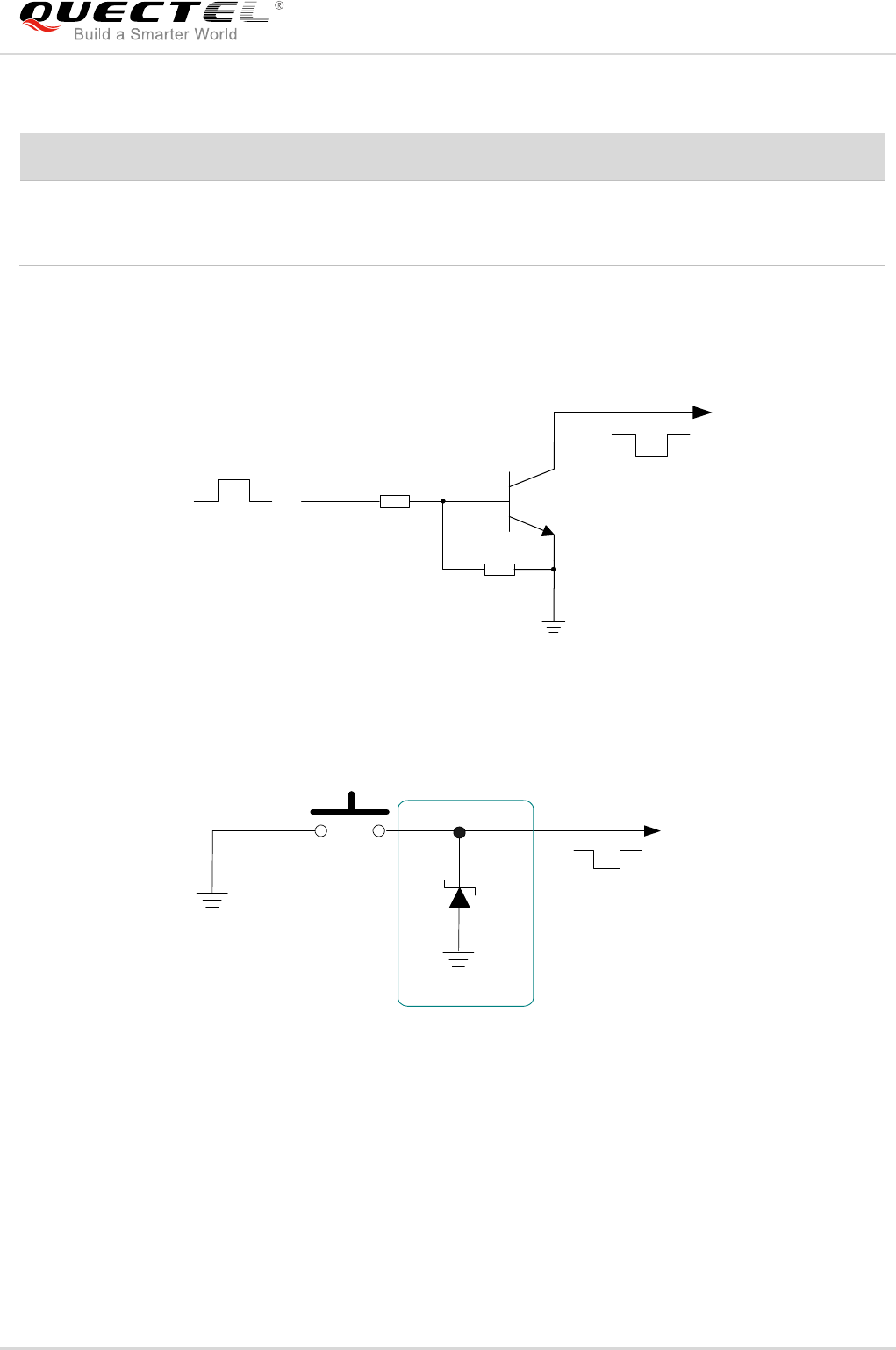
LTE-A Module Series
EG06 Hardware Design
EG06_Hardware_Design 41 / 89
Table 8: RESET_N Pin Description
The recommended circuit is similar to the PWRKEY control circuit. An open drain/collector driver or button
can be used to control the RESET_N.
Reset pulse
RESET_N
4.7K
47K
250ms~600ms
Figure 15: Reference Circuit of RESET_N by Using Driving Circuit
RESET_N
S2
Close to S2
TVS
Figure 16: Reference Circuit of RESET_N by Using Button
Pin Name
Pin No.
Description
DC Characteristics
Comment
RESET_N
1
Reset the module
VIHmax=2.1V
VIHmin=1.3V
VILmax=0.5V
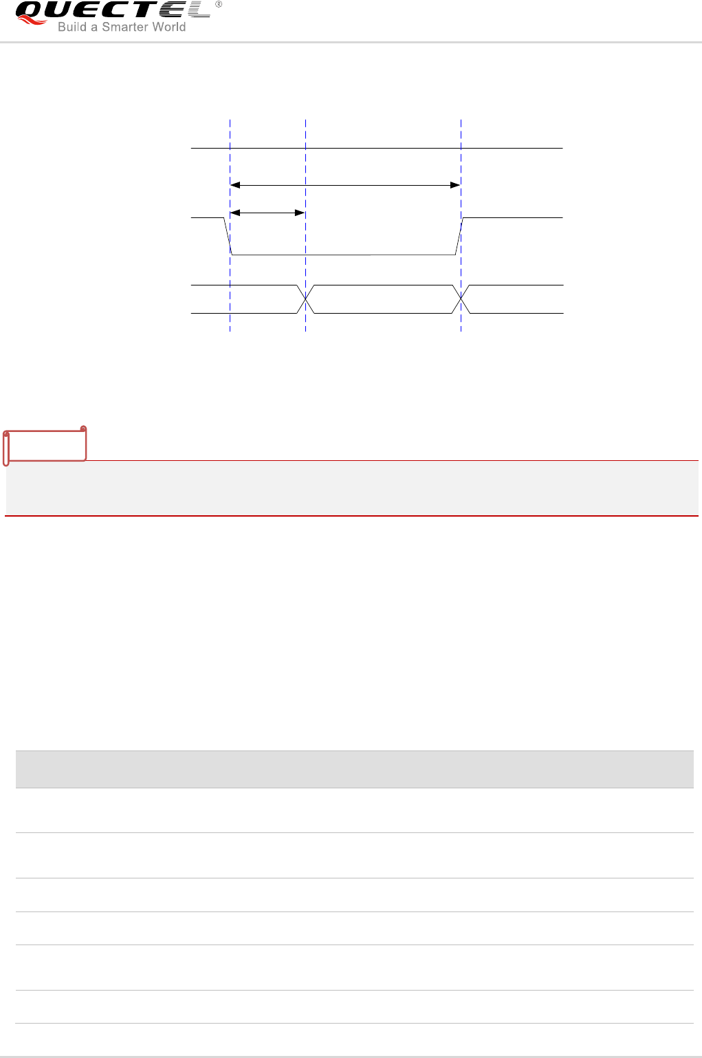
LTE-A Module Series
EG06 Hardware Design
EG06_Hardware_Design 42 / 89
The reset scenario is illustrated in the following figure.
VIL≤0.5V
VIH≥1.3V
VBAT
≥250ms
Resetting
Module
Status Running
RESET_N
Restart
≤600ms
Figure 17: Timing of Resetting Module
1. Use RESET_N only when turning off the module by AT+QPOWD command and PWRKEY pin failed.
2. Ensure that there is no large capacitance on PWRKEY and RESET_N pins.
3.9. (U)SIM Interface
The (U)SIM interface circuitry meets ETSI and IMT-2000 requirements. Either 1.8V or 3.0V (U)SIM cards
are supported.
Table 9: Pin Definition of the (U)SIM Interface
Pin Name
Pin No.
I/O
Description
Comment
USIM_VDD
26
PO
Power supply for (U)SIM card
Either 1.8V or 3.0V is supported
by the module automatically.
USIM_
DATA
29
IO
Data signal of (U)SIM card
USIM_CLK
27
DO
Clock signal of (U)SIM card
USIM_RST
28
DO
Reset signal of (U)SIM card
USIM_
PRESENCE
25
DI
(U)SIM card insertion detection
USIM_GND
24
Specified ground for (U)SIM card
NOTES
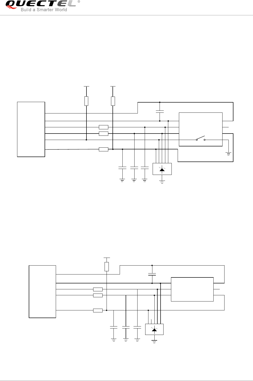
LTE-A Module Series
EG06 Hardware Design
EG06_Hardware_Design 43 / 89
EG06 supports (U)SIM card hot-plug via the USIM_PRESENCE pin. The function supports low level and
high level detections, and is disabled by default. Please refer to document [1] about AT+QSIMDET
command for details.
The following figure shows a reference design for (U)SIM card interface with an 8-pin (U)SIM card
connector.
Module
USIM_VDD
USIM_GND
USIM_RST
USIM_CLK
USIM_DATA
USIM_PRESENCE
22R
22R
22R
VDD_EXT
51K
100nF (U)SIM Card Connector
GND
GND
VCC
RST
CLK IO
VPP
GND
USIM_VDD
15K
NM NM NM
Figure 18: Reference Circuit of (U)SIM Interface with an 8-Pin (U)SIM Card Connector
If (U)SIM card detection function is not needed, please keep USIM_PRESENCE unconnected. A
reference circuit for (U)SIM interface with a 6-pin (U)SIM card connector is illustrated in the following
figure.
Module
USIM_VDD
USIM_GND
USIM_RST
USIM_CLK
USIM_DATA 22R
22R
22R
100nF (U)SIM Card Connector
GND
VCC
RST
CLK IO
VPP
GND
15K
USIM_VDD
NM NM
NM
Figure 19: Reference Circuit of (U)SIM Interface with a 6-Pin (U)SIM Card Connector

LTE-A Module Series
EG06 Hardware Design
EG06_Hardware_Design 44 / 89
In order to enhance the reliability and availability of the (U)SIM card in applications, please follow the
criteria below in the (U)SIM circuit design:
Keep placement of (U)SIM card connector to the module as close as possible. Keep the trace length
as less than 200mm as possible.
Keep (U)SIM card signals away from RF and VBAT traces.
Make sure the ground between the module and the (U)SIM card connector short and wide. Keep the
trace width of ground and USIM_VDD no less than 0.5mm to maintain the same electric potential.
To avoid cross-talk between USIM_DATA and USIM_CLK, keep them away from each other and
shield them with surrounded ground.
In order to offer good ESD protection, it is recommended to add a TVS diode array of which parasitic
capacitance should not be more than 50pF. The 22Ω resistors should be added in series between the
module and the (U)SIM card to facilitate debugging. Please note that the (U)SIM peripheral circuit
should be close to the (U)SIM card connector.
The pull-up resistor on USIM_DATA line can improve anti-jamming capability when long layout trace
and sensitive occasion are applied, and should be placed close to the (U)SIM card connector.
3.10. USB Interface
EG06 provides one integrated Universal Serial Bus (USB) interface which complies with the USB 3.0/2.0
specifications and supports super speed (5Gbps) on USB 3.0, high speed (480 Mbps) and full speed (12
Mbps) modes on USB 2.0. The USB interface is used for AT command communication, data transmission,
GNSS NMEA output, software debugging, firmware upgrade and voice over USB*.
The following table shows the pin definition of USB interface.
Table 10: Pin Description of USB Interface
Pin Name
Pin No.
I/O
Description
Comment
USB Signal Part
USB_DP
34
IO
USB 2.0 differential data bus - plus
Require differential
impedance of 90Ω
USB_DM
33
IO
USB 2.0 differential data bus - minus
USB_VBUS
32
PI
Used for detecting the USB connection
Typical 5.0V
USB_ID
36
DI
OTG identification
USB_SS_
TX_P
38
AO
USB 3.0 super-speed transmit - plus
Require differential
impedance of 90Ω
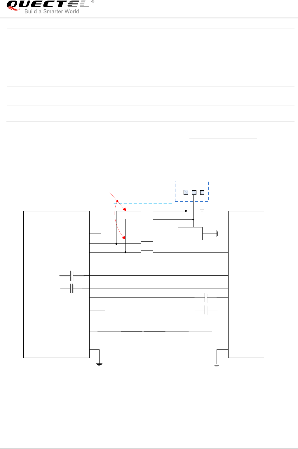
LTE-A Module Series
EG06 Hardware Design
EG06_Hardware_Design 45 / 89
For more details about the USB 2.0&3.0 specifications, please visit http://www.usb.org/home.
The USB interface is recommended to be reserved for firmware upgrade in customers’ designs. The
following figure shows a reference circuit of USB 2.0 & USB 3.0 interface.
USB_DP
USB_DM
GND
USB_DP
USB_DM
GND
R1
R2
Close to Module
R3
R4
Test Points
ESD Array
NM_0R
NM_0R
0R
0R
Minimize these stubs
Module MCU
USB_VBUS
VDD
USB_SS_TX_P
USB_SS_TX_M
USB_SS_RX_P
USB_SS_RX_M
C1
C2
C3
C4
100nF
100nF
100nF
100nF
USB_SS_RX_P
USB_SS_RX_M
USB_SS_TX_P
USB_SS_TX_M
USB_ID GPIO
Figure 20: Reference Circuit of USB Application
In order to ensure the signal integrity of USB data lines, components R1, R2, R3, R4 must be placed
close to the module, the two capacitors of C1 and C2 have been placed inside the module,C3 and C4
components must be placed close to the MCU, and also these resistors should be placed close to each
USB_SS_
TX_M
37
AO
USB 3.0 super-speed transmit - minus
USB_SS_
RX_P
40
AI
USB 3.0 super-speed receive -plus
Require differential
impedance of 90Ω
USB_SS_
RX_M
41
AI
USB 3.0 super-speed receive -minus
OTG_PWR_
EN
143
DO
OTG power control
GND
35
Ground
LTE-A Module Series
EG06 Hardware Design
EG06_Hardware_Design 46 / 89
other. The extra stubs of trace must be as short as possible.
The following principles should be complied with when design the USB interface, so as to meet USB 2.0 &
USB 3.0 specifications.
It is important to route the USB signal traces as differential pairs with total grounding. The impedance
of USB differential trace is 90Ω.
For USB 3.0 routing traces, the length matching of Tx and Rx differential pairs should be less than
0.7mm.
Do not route signal traces under crystals, oscillators, magnetic devices, PCIe and RF signal traces. It
is important to route the USB differential traces in inner-layer with ground shielding on not only upper
and lower layers but also right and left sides.
Pay attention to the influence of junction capacitance of ESD protection components on USB data
lines. Typically, the capacitance value should be less than 2.0pF for USB 2.0, and less than 0.4pF for
USB 3.0.
Keep the ESD protection components to the USB connector as close as possible.
If possible, reserve a 0R resistor on USB_DP and USB_DM lines.
“*” means under development.
3.11. UART Interfaces
The module provides three UART interfaces: the main UART interface, the debug UART interface, and
the BT UART interface. The following shows their features.
The main UART interface supports 4800bps, 9600bps, 19200bps, 38400bps, 57600bps, 115200bps,
230400bps, 460800bps and 921600bps baud rates, and the default is 115200bps. This interface is
used for data transmission and AT command communication.
The debug UART interface supports 115200bps baud rate. It is used for Linux console and log
output.
The BT UART interface supports 115200bps baud rate. It is used for BT communication.
The following tables show the pin definition.
Table 11: Pin Definition of the Main UART Interface
Pin Name
Pin No.
I/O
Description
Comment
RI
61
DO
Ring indicator
1.8V power domain
NOTE
LTE-A Module Series
EG06 Hardware Design
EG06_Hardware_Design 47 / 89
Table 12: Pin Definition of the Debug UART Interface
Table 13: Pin Definition of the BT UART Interface
The logic levels are described in the following table.
Table 14: Logic Levels of Digital I/O
DCD
59
DO
Data carrier detection
1.8V power domain
CTS
56
DO
Clear to send
1.8V power domain
RTS
57
DI
Request to send
1.8V power domain
DTR
62
DI
Data terminal ready,
Sleep mode control
1.8V power domain
TXD
60
DO
Transmit data
1.8V power domain
RXD
58
DI
Receive data
1.8V power domain
Pin Name
Pin No.
I/O
Description
Comment
DBG_TXD
137
DO
Transmit data
1.8V power domain
DBG_RXD
136
DI
Receive data
1.8V power domain
Pin Name
Pin No.
I/O
Description
Comment
BT_TXD
163
DO
Transmit data
1.8V power domain
BT_RXD
165
DI
Receive data
1.8V power domain
BT_CTS
164
DO
Clear to send
1.8V power domain
BT_RTS
166
DI
Request to send
1.8V power domain
Parameter
Min.
Max.
Unit
VIL
-0.3
0.6
V
VIH
1.2
2.0
V
VOL
0
0.45
V
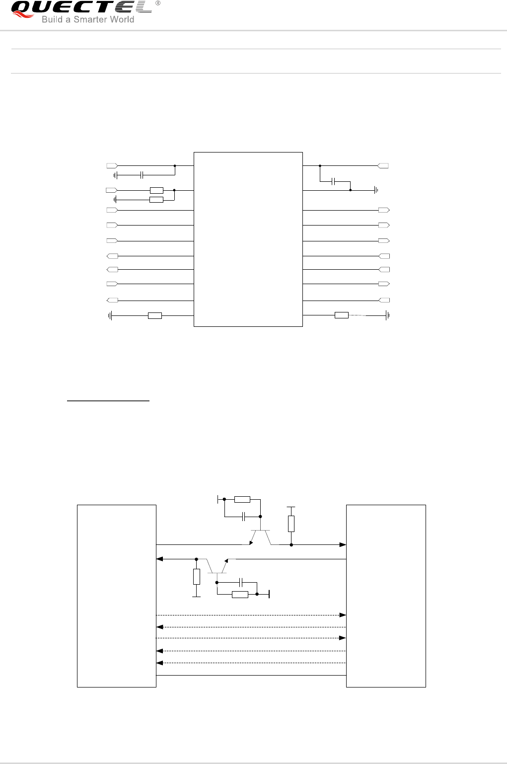
LTE-A Module Series
EG06 Hardware Design
EG06_Hardware_Design 48 / 89
The module provides 1.8V UART interface. A level translator should be used if the application is equipped
with a 3.3V UART interface. A level translator TXS0108EPWR provided by Texas Instruments is
recommended. The following figure shows a reference design.
VCCA VCCB
OE
A1
A2
A3
A4
A5
A6
A7
A8
GND
B1
B2
B3
B4
B5
B6
B7
B8
VDD_EXT
RI
DCD
RTS
RXD
DTR
CTS
TXD
51K 51K
0.1uF 0.1uF
RI_MCU
DCD_MCU
RTS_MCU
TXD_MCU
DTR_MCU
CTS_MCU
RXD_MCU
VDD_MCU
Translator
VDD_EXT 10K
120K
Figure 21: Reference Circuit with Translator Chip
Please visit http://www.ti.com for more information.
Another example with transistor translation circuit is shown as below. The circuit design of dotted line
section can refer to the design of solid line section, in terms of both module input and output circuit
designs, but please pay attention to the direction of connection.
MCU/ARM
TXD
RXD
VDD_EXT
10K
VCC_MCU 4.7K
10K
VDD_EXT
TXD
RXD
RTS
CTS
DTR
RI
RTS
CTS
GND
GPIO DCD
Module
GPIO
EINT
VDD_EXT
4.7K
GND
1nF
1nF
Figure 22: Reference Circuit with Transistor Circuit
VOH
1.35
1.8
V
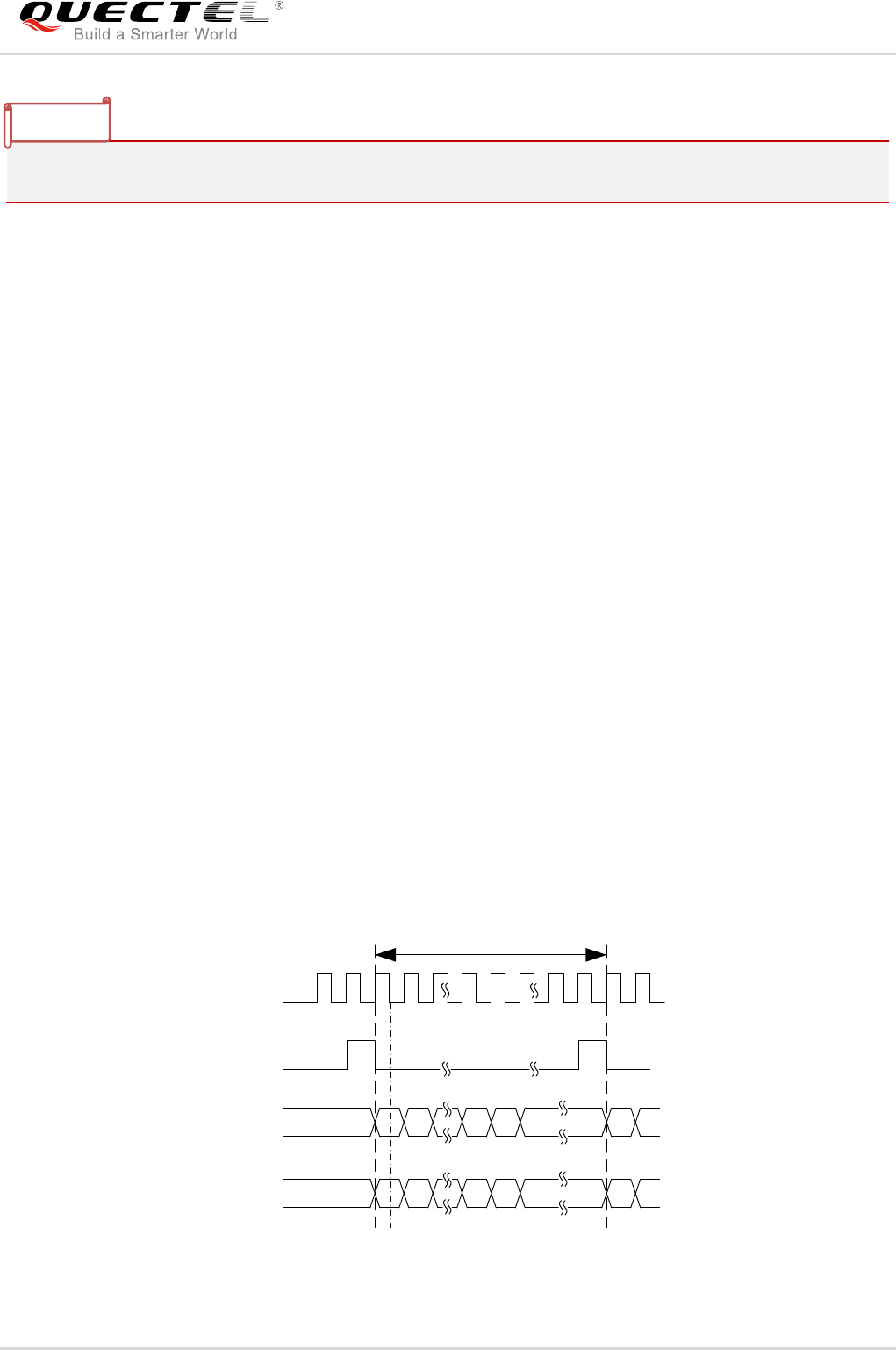
LTE-A Module Series
EG06 Hardware Design
EG06_Hardware_Design 49 / 89
Transistor circuit solution is not suitable for applications with high baud rates exceeding 460Kbps.
3.12. PCM and I2C Interfaces
EG06 supports audio communication via Pulse Code Modulation (PCM) digital interface and I2C
interface.
The PCM interface supports the following modes:
Primary mode (short frame synchronization, works as both master and slave)
Auxiliary mode (long frame synchronization, works as master only)
In primary mode, the data is sampled on the falling edge of the PCM_CLK and transmitted on the rising
edge. The PCM_SYNC falling edge represents the MSB. In this mode, the PCM interface supports
256kHz, 512kHz, 1024kHz or 2048kHz PCM_CLK at 8kHz PCM_SYNC, and also supports 4096kHz
PCM_CLK at 16kHz PCM_SYNC.
In auxiliary mode, the data is sampled on the falling edge of the PCM_CLK and transmitted on the rising
edge. The PCM_SYNC rising edge represents the MSB. In this mode, PCM interface operates with a
256kHz PCM_CLK and an 8kHz, 50% duty cycle PCM_SYNC only.
EG06 supports 16-bit linear data format. The following figures show the primary mode’s timing
relationship with 8kHz PCM_SYNC and 2048kHz PCM_CLK, as well as the auxiliary mode’s timing
relationship with 8kHz PCM_SYNC and 256kHz PCM_CLK.
PCM_CLK
PCM_SYNC
PCM_OUT
MSB LSB MSB
125us
1 2 256255
PCM_IN
MSB
LSBMSB
Figure 23: Primary Mode Timing
NOTE
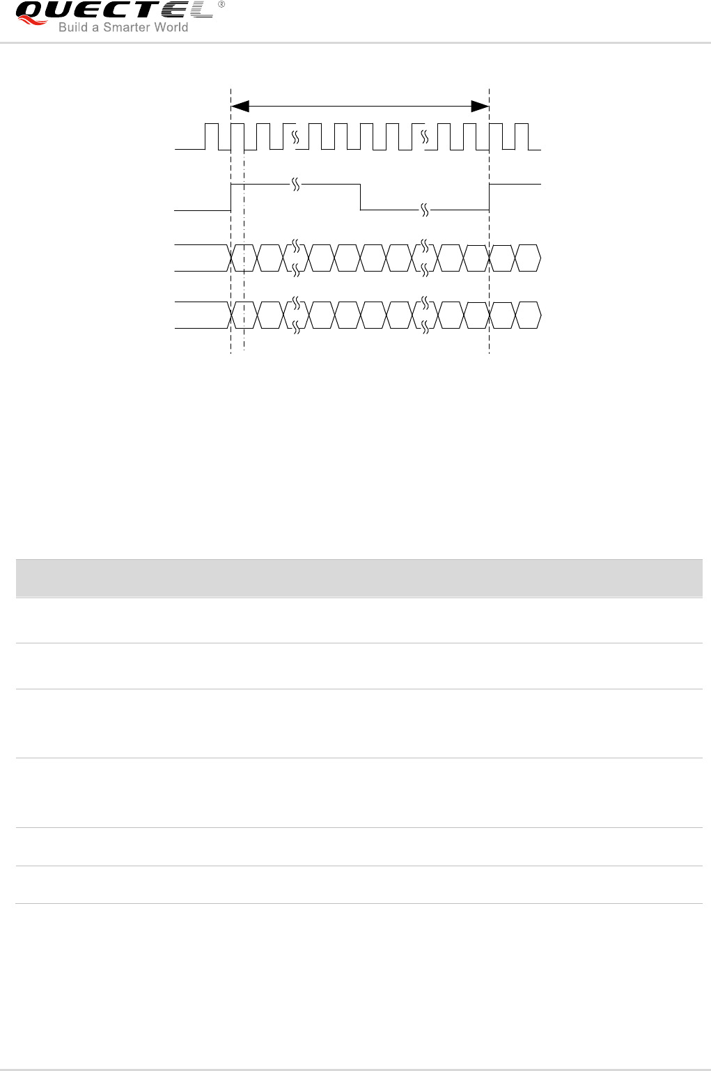
LTE-A Module Series
EG06 Hardware Design
EG06_Hardware_Design 50 / 89
PCM_CLK
PCM_SYNC
PCM_OUT
MSB LSB
PCM_IN
125us
MSB
1 2 3231
LSB
Figure 24: Auxiliary Mode Timing
The following table shows the pin definition of PCM and I2C interfaces which can be applied on audio
codec design.
Table 15: Pin Definition of PCM and I2C Interfaces
Clock and mode can be configured by AT command, and the default configuration is master mode using
short frame synchronization format with 2048kHz PCM_CLK and 8kHz PCM_SYNC. Please refer to
document [1] for details about AT+QDAI command.
Pin Name
Pin No.
I/O
Description
Comment
PCM_IN
66
DI
PCM data input
1.8V power domain.
If unused, keep it open.
PCM_OUT
68
DO
PCM data output
1.8V power domain.
If unused, keep it open.
PCM_SYNC
65
IO
PCM data frame
synchronization
signal
1.8V power domain. In master mode, it
is an output signal. In slave mode, it is
an input signal.
If unused, keep it open.
PCM_CLK
67
IO
PCM data bit clock
1.8V power domain. In master mode, it
is an output signal. In slave mode, it is
an input signal.
If unused, keep it open.
I2C_SCL
43
OD
I2C serial clock
Require an external pull-up to 1.8V
I2C_SDA
42
OD
I2C serial data
Require an external pull-up to 1.8V
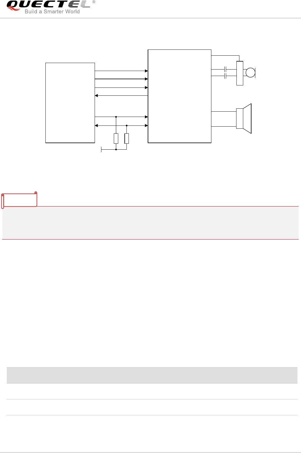
LTE-A Module Series
EG06 Hardware Design
EG06_Hardware_Design 51 / 89
The following figure shows a reference design of PCM interface with an external codec IC.
PCM_IN
PCM_OUT
PCM_SYNC
PCM_CLK
I2C_SCL
I2C_SDA
Module
1.8V
4.7K
4.7K
BCLK
LRCK
DAC
ADC
SCL
SDA
BIAS
MICBIAS
INP
INN
LOUTP
LOUTN
Codec
Figure 25: Reference Circuit of PCM Application with Audio Codec
1. It is recommended to reserve an RC (R=22Ω, C=22pF) circuit on the PCM lines, especially for
PCM_CLK.
2. EG06 works as a master device pertaining to I2C interface.
3.13. ADC Interfaces
The module provides two Analog-to-Digital Converters (ADC) interfaces. AT+QADC=0 command can be
used to read the voltage value on ADC0 pin. AT+QADC=1 command can be used to read the voltage
value on ADC1 pin. For more details about these AT+QADC command, please refer to document [1].
In order to improve the accuracy of ADC, the trace of ADC should be surrounded by ground.
Table 16: Pin Definition of the ADC Interfaces
Pin Name
Pin No.
Description
ADC0
173
General purpose analog to digital converter
ADC1
175
General purpose analog to digital converter
NOTES
LTE-A Module Series
EG06 Hardware Design
EG06_Hardware_Design 52 / 89
The following table describes the characteristic of the ADC interfaces.
Table 17: Characteristics of ADC Interfaces
1. The input voltage of ADC should not exceed that of VBAT_BB.
2. It is prohibited to supply any voltage to ADC pins when VBAT is removed.
3. It is recommended to use resistor divider circuit for ADC application.
3.14. Network Status Indication
The network indication pins can be used to drive network status indication LEDs. The module provides
two pins which are NET_MODE and NET_STATUS. The following tables describe pin definition and logic
level changes in different network status.
Table 18: Pin Definition of Network Connection Status/Activity Indicator
Table 19: Working State of the Network Connection Status/Activity Indicator
Parameter
Min.
Typ.
Max.
Unit
ADC0 Voltage Range
0.15
VBAT_BB
V
ADC1 Voltage Range
0.15
VBAT_BB
V
ADC Resolution
15
bits
Pin Name
Pin No.
I/O
Description
Comment
NET_MODE
147
DO
Indicate the module’s network
registration mode.
1.8V power domain
NET_STATUS
170
DO
Indicate the module’s network activity
status.
1.8V power domain
Pin Name
Status
Description
NET_MODE
Always High
Registered on LTE network
NOTES
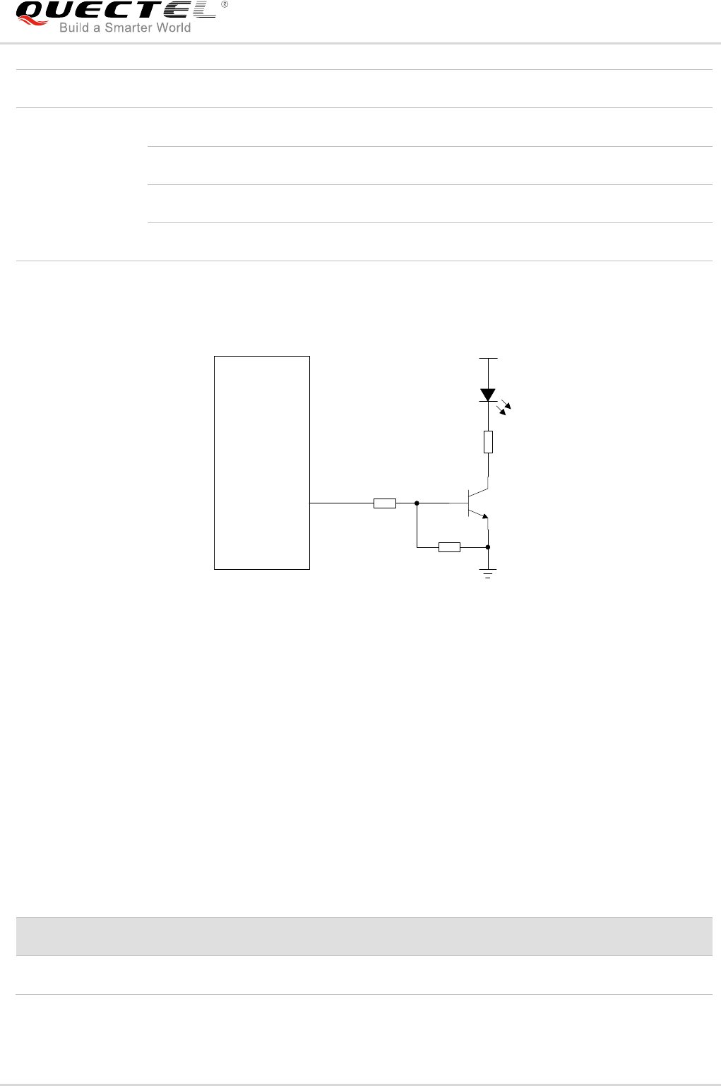
LTE-A Module Series
EG06 Hardware Design
EG06_Hardware_Design 53 / 89
A reference circuit is shown in the following figure.
4.7K
47K
VBAT
2.2K
Module
Network
Indicator
Figure 26: Reference Circuit of the Network Indicator
3.15. STATUS
The STATUS pin is set as the module status indicator. It will output high level when module is powered
on.
The following table describes pin definition of STATUS.
Table 20: Pin Definition of STATUS
Always Low
Others
NET_STATUS
Flicker slowly (200ms High/1800ms Low)
Network searching
Flicker slowly (1800ms High/200ms Low)
Idle
Flicker quickly (125ms High/125ms Low)
Data transfer is ongoing
Always High
Voice calling
Pin Name
Pin No.
I/O
Description
Comment
STATUS
171
DO
Indicate the module’s operation status
1.8V power domain
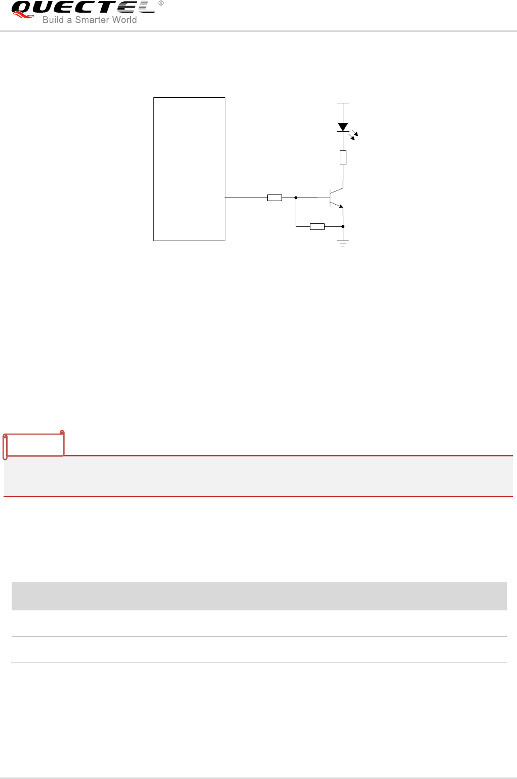
LTE-A Module Series
EG06 Hardware Design
EG06_Hardware_Design 54 / 89
A reference circuit is shown as below.
4.7K
47K
VBAT
2.2K
Module
STATUS
Figure 27: Reference Circuits of STATUS
3.16. Behavior of the RI
AT+QCFG="risignaltype","physical" command can be used to configure RI behavior.
No matter on which port a URC is presented, the URC will trigger the behavior of RI pin.
The URC can be output from UART port, USB AT port and USB modem port by AT+QURCCFG
command. The default port is USB AT port.
In addition, RI behavior can be configured flexibly. The default behavior of the RI is shown as below.
Table 21: Behavior of the RI
State
Response
Idle
RI keeps at high level
URC
RI outputs 120ms low pulse when a new URC returns
The RI behavior can be changed by AT+QCFG="urc/ri/ring" command. Please refer to document [1]
for details.
NOTE

LTE-A Module Series
EG06 Hardware Design
EG06_Hardware_Design 55 / 89
3.17. PCIe Interface*
EG06 includes a PCIe interface which is compliant with PCI Express Specification Revision 2.1. The key
features of the PCIe interface are shown below:
PCI Express Specification Revision 2.1 compliance
Data rate at 5Gbps per lane
Can be used to connect to an external Ethernet IC (MAC and PHY) or WLAN IC.
The following table shows the pin definition of PCIe interface.
Table 22: Pin Definition of the PCIe Interface
In order to enhance the reliability and availability in applications, please follow the criteria below in the
PCIe interface circuit design:
Pin Name
Pin No.
I/O
Description
Comment
Control Signal Part
PCIE_REF
CLK_P
179
AO
Output PCIe reference clock - plus
If unused, keep it open.
PCIE_REF
CLK_M
180
AO
Output PCIe reference clock - minus
If unused, keep it open.
PCIE_TX_M
182
AO
PCIe transmit - minus
If unused, keep it open.
PCIE_TX_P
183
AO
PCIe transmit - plus
If unused, keep it open.
PCIE_RX_M
185
AI
PCIe receive - minus
If unused, keep it open.
PCIE_RX_P
186
AI
PCIe receive -plus
If unused, keep it open.
PCIE_CLK_
REQ_N
188
IO
PCIe clock request
In master mode, it is an input
signal.
In slave mode, it is an output
signal.
If unused, keep it open.
PCIE_RST_N
189
IO
PCIe reset
In master mode, it is an
output signal.
In slave mode, it is an input
signal.
If unused, keep it open.
PCIE_WAKE
_N
190
IO
PCIe wake
In master mode, it is an input
signal.
In slave mode, it is an output
signal.
If unused, keep it open.
LTE-A Module Series
EG06 Hardware Design
EG06_Hardware_Design 56 / 89
Keep PCIe data and control signals away from sensitive circuits and signals, such as RF, audio, and
19.2MHz clock signals.
A capacitance should be added in series on Tx/Rx traces to remove any DC bias.
Keep the maximum trace length less than 300mm.
The length difference of Tx or Rx differential pairs should be less than 0.7mm for PCIe routing traces.
The differential impedance of PCIe data trace should be 100Ω±10%.
Separate the SS-USB data pairs (Tx, Rx) and PCIe data pairs (Tx, Rx) from each other as far as
possible. If SS_USB and PCIe data pairs must cross on adjacent layers, please keep crossings at
right angles to minimize unbalanced (asymmetric) coupling.
PCIe data traces must not be routed under components or crossing other traces.
“*” means under development.
3.18. WLAN Control Interface*
EG06 provides a low power PCIe interface* and a control interface for WLAN design.
The following table shows the pin definition of WLAN control interface.
Table 23: Pin Definition of WLAN Control Interface
Pin Name
Pin No.
I/O
Description
Comment
Coexistence and Control Signal Part
PM_ENABLE
5
DO
External power enable control
1.8V power domain
WAKE_ON_
WIRELESS
160
DI
Wake up the host (EG06 module)
by Wi-Fi module.
1.8V power domain
WLAN_EN
149
DO
WLAN function enable control.
Active high.
1.8V power domain
COEX_UART_RX
146
DI
LTE/WLAN coexistence signal
1.8V power domain
COEX_UART_TX
145
DO
LTE/WLAN coexistence signal
1.8V power domain
WLAN_SLP_CLK
169
DO
WLAN sleep clock
1.8V power domain
NOTE
LTE-A Module Series
EG06 Hardware Design
EG06_Hardware_Design 57 / 89
“*” means under development.
3.19. SD Card Interface
EG06 provides one SD card interface which supports SD 3.0 protocol. The following tables show the pin
definition.
Table 24: Pin Definition of the SD CardInterface
Pin Name
Pin No.
I/O
Description
Comment
SD_DATA3
48
IO
Secure digital controller data bit 3
SD_DATA2
47
IO
Secure digital controller data bit 2
SD_DATA1
50
IO
Secure digital controller data bit 1
SD_DATA0
49
IO
Secure digital controller data bit 0
SD_CLK
53
DO
Serial clock signal for SD card
SD_CMD
51
IO
Command signal for SD card
SD_VDD
46
PO
Power supply for pull up voltage of SD
bus
1.8V/2.85V configurable
output. Cannot be used
for SD card power supply.
SD_DETECT
52
DI
SD card insertion detection
NOTE
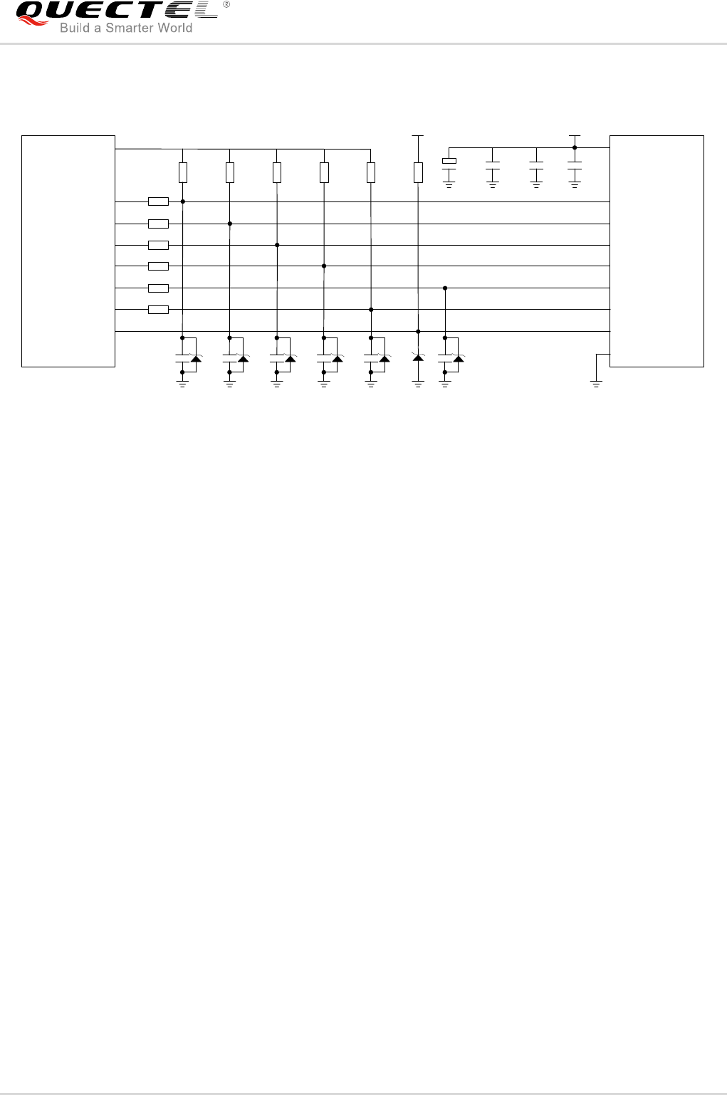
LTE-A Module Series
EG06 Hardware Design
EG06_Hardware_Design 58 / 89
The following figure shows a reference design of SD card interface with EG06 module.
SD Card Connector
DAT2
CD/DAT3
CMD
VDD
CLK
VSS
DAT0
DAT1
DETECTIVE
Module
SD_DATA3
SD_DATA2
SD_DATA1
SD_VDD
SD_DATA0
SD_CLK
SD_CMD
SD_DETECT
R1 0R
R7
100K R8
100K R9
100K R10
100K R11
100K R12
470K
VDD_EXT VDD_2V85
R2 0R
R3 0R
R4 0R
R5 0R
R6 0R
C2
NM D2 C3
NM D3 C4
NM D4 C5
NM D5 C6
NM D6
C1
NM D1
C7
10pF
D7
C8
33pF
C9
100nF
C10
100uF
+
Figure 28: Reference Circuit of SD Card Application
Please follow the principles below in the SD card circuit design:
The voltage range of SD power supply VDD_2V85 is 2.7V~3.6V and a sufficient current up to 0.8A
should be provided. As the maximum output current of VDD_SDIO is 50mA which can only be used
for SDIO pull-up resistors, an external power supply is needed for SD card.
To avoid jitter of bus, resistors R7~R11 are needed to pull up the SDIO to SD_VDD. Value of these
resistors is among 10kΩ~100kΩ and the recommended value is 100kΩ.
In order to improve signal quality, it is recommended to add 0Ω resistors R1~R6 in series between
the module and the SD card. The bypass capacitors C1~C6 are reserved and not mounted by default.
All resistors and bypass capacitors should be placed close to the module.
In order to offer good ESD protection, it is recommended to add a TVS diode on SD card pins.
The load capacitance of SDIO bus needs to be less than 40pF.
It is important to route the SDIO signal traces with total grounding. The impedance of SDIO data
trace is 50Ω (±10%).
Keep SDIO signals far away from other sensitive circuits/signals such as RF circuits, analog signals,
etc., as well as noisy signals such as clock signals, DCDC signals, etc.
It is recommended to keep the trace length difference between CLK and DATA/CMD less than 1mm
and the total routing length less than 50mm. The total trace length inside the module is 36mm, so the
exterior total trace length should be less than 14mm.
Make sure the adjacent trace spacing is two times of the trace width and the load capacitance of
SDIO bus should be less than 40pF.
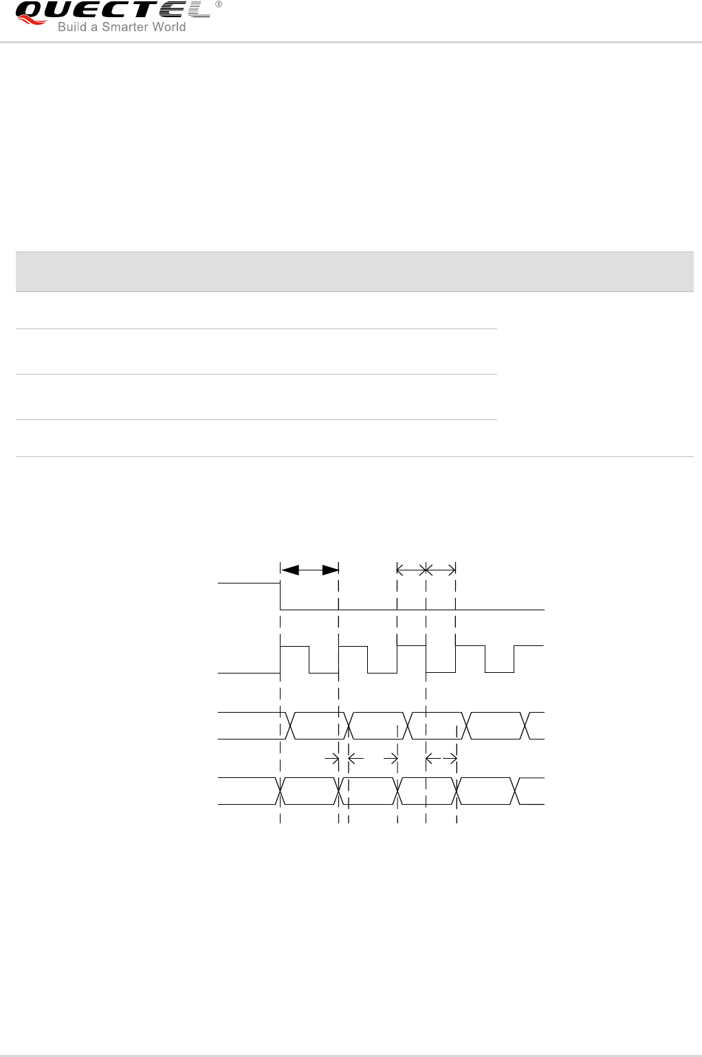
LTE-A Module Series
EG06 Hardware Design
EG06_Hardware_Design 59 / 89
3.20. SPI Interface
EG06 provides one SPI interface which only supports master mode with a maximum clock frequency up
to 50MHz. The following table shows the pin definition of SPI interface.
Table 25: Pin Definition of the SPI Interface
The following figure shows the timing relationship of SPI interface. The related parameters of SPI timing is
shown as the following table.
SPI_CS_N
SPI_CLK
SPI_MOSI
MSB
1 2
SPI_MISO
3
T
t(mov)
4
t(mis) t(mih)
t(ch) t(cl)
Figure 29: SPI Interface Timing
Pin Name
Pin No.
I/O
Description
Comment
SPI_CS
79
DO
Chip select of SPI interface
1.8V power domain.
If unused, keep them open.
SPI_MOSI
77
DO
Master output slave input of SPI
interface
SPI_MISO
78
DI
Master input slave output of SPI
interface
SPI_CLK
80
DO
Clock signal of SPI interface
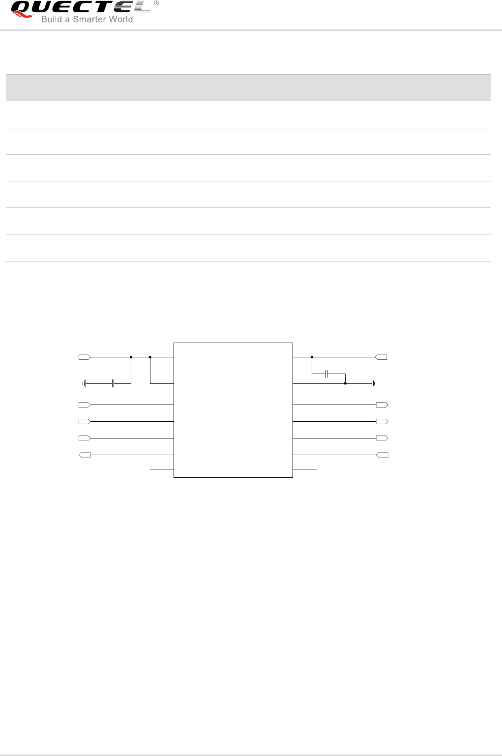
LTE-A Module Series
EG06 Hardware Design
EG06_Hardware_Design 60 / 89
Table 26: Parameters of SPI Interface Timing
The module provides a 1.8V SPI interface. A level translator between the module and host should be
used if the application is equipped with a 3.3V processor or device interface. The following figure shows a
reference design.
VCCA VCCB
OE
A1
A2
A3
A4
NC
GND
B1
B2
B3
B4
NC
VDD_EXT
SPI_CS
SPI_CLK
SPI_MISO
SPI_MOSI
0.1uF 0.1uF
SPI_CS_N_MCU
SPI_CLK_MCU
SPI_MISO_MCU
SPI_MOSI_MCU
VDD_MCU
Translator
Figure 30: SPI Interface Reference Circuit with a Level Translator
3.21. USB_BOOT Interface
EG06 provides a USB_BOOT pin. Developers can pull up USB_BOOT to VDD_EXT before powering on
the module, thus the module will enter into emergency download mode when powered on. In this mode,
the module supports firmware upgrade over USB interface.
Parameter
Description
Min.
Typ.
Max.
Unit
T
SPI clock period
20.0
-
-
ns
t(ch)
SPI clock high level time
9.0
-
-
ns
t(cl)
SPI clock low level time
9.0
-
-
ns
t(mov)
SPI master data output valid time
-5.0
-
5.0
ns
t(mis)
SPI master data input setup time
5.0
-
-
ns
t(mih)
SPI master data input hold time
1.0
-
-
ns
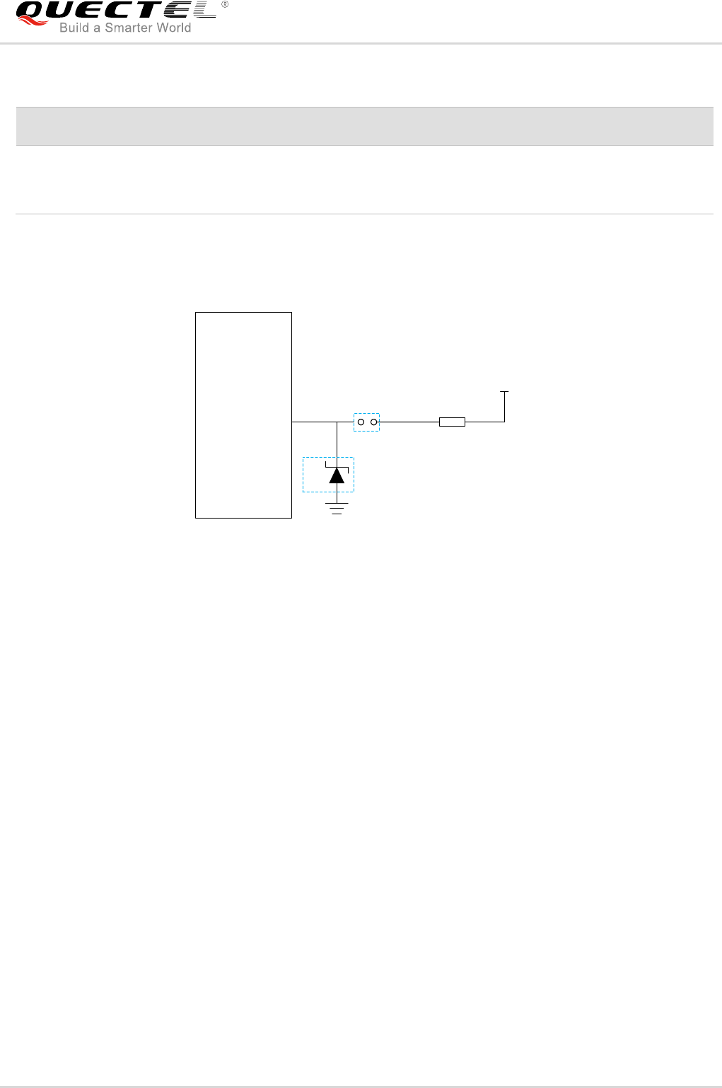
LTE-A Module Series
EG06 Hardware Design
EG06_Hardware_Design 61 / 89
Table 27: Pin Definition of USB_BOOT Interface
The following figure shows a reference circuit of USB_BOOT interface.
Module
USB_BOOT
VDD_EXT
10K
Test point
TVS Close to module
Figure 31: Reference Circuit of USB_BOOT Interface
Pin Name
Pin No.
I/O
Description
Comment
USB_BOOT
140
DI
Force the module to enter into
emergency download mode
1.8V power domain.
Active high.
If unused, keep it open.

LTE-A Module Series
EG06 Hardware Design
EG06_Hardware_Design 62 / 89
4 GNSS Receiver
4.1. General Description
EG06 includes a fully integrated global navigation satellite system solution that supports Gen8C-Lite of
Qualcomm (GPS, GLONASS, BeiDou, Galileo and QZSS).
EG06 supports standard NMEA-0183 protocol, and outputs NMEA sentences at 1Hz data update rate via
USB interface by default.
By default, EG06 GNSS engine is switched off. It has to be switched on via AT command. For more
details about GNSS engine technology and configurations, please refer to document [2].
4.2. GNSS Performance
The following table shows GNSS performance of EG06.
Table 28: GNSS Performance
Parameter
Description
Conditions
Typ.
Unit
Sensitivity
(GNSS)
Cold start
Autonomous
TBD
dBm
Reacquisition
Autonomous
TBD
dBm
Tracking
Autonomous
TBD
dBm
TTFF
(GNSS)
Cold start
@open sky
Autonomous
TBD
s
XTRA enabled
TBD
s
Warm start
@open sky
Autonomous
TBD
s
XTRA enabled
TBD
s
LTE-A Module Series
EG06 Hardware Design
EG06_Hardware_Design 63 / 89
1. Tracking sensitivity: the lowest GNSS signal value at the antenna port on which the module can keep
on positioning for 3 minutes.
2. Reacquisition sensitivity: the lowest GNSS signal value at the antenna port on which the module can
fix position again within 3 minutes after loss of lock.
3. Cold start sensitivity: the lowest GNSS signal value at the antenna port on which the module fixes
position within 3 minutes after executing cold start command.
4.3. Layout Guidelines
The following layout guidelines should be taken into account in customers’ design.
Maximize the distance among GNSS antenna, main antenna and Rx-diversity antenna.
Digital circuits such as (U)SIM card, USB interface, camera module, display connector and SD card
should be kept away from the antennas.
Use ground vias around the GNSS trace and sensitive analog signal traces to provide coplanar
isolation and protection.
Keep the characteristic impedance for ANT_GNSS trace as 50Ω.
Please refer to Chapter 5 for GNSS reference design and antenna installation information.
Hot start
@open sky
Autonomous
TBD
s
XTRA enabled
TBD
s
Accuracy
(GNSS)
CEP-50
Autonomous
@open sky
TBD
m
NOTES

LTE-A Module Series
EG06 Hardware Design
EG06_Hardware_Design 64 / 89
5 Antenna Interfaces
EG06 includes a main antenna interface, an Rx-diversity antenna interface which is used to resist the fall
of signals caused by high speed movement and multipath effect, and a GNSS antenna interface. The
impedance of antenna port is 50Ω.
5.1. Main/Rx-diversity Antenna Interface
5.1.1. Pin Definition
The pin definition of main antenna and Rx-diversity antenna interfaces are shown below.
Table 29: Pin Definition of the RF Antenna
5.1.2. Operating Frequency
Table 30: Module Operating Frequencies
Pin Name
Pin No.
I/O
Description
Comment
ANT_MAIN
107
IO
Main antenna pad
50Ω impedance
ANT_DIV
127
AI
Receive diversity antenna pad
50Ω impedance
3GPP Band
Transmit
Receive
Unit
WCDMA B1
1920~1980
2110~2170
MHz
WCDMA B2
1850~1910
1930~1990
MHz
WCDMA B3
1710~1785
1805~1880
MHz
WCDMA B4
1710~1755
2110~2155
MHz
WCDMA B5
824~849
869~894
MHz
WCDMA B6
830~840
875~885
MHz

LTE-A Module Series
EG06 Hardware Design
EG06_Hardware_Design 65 / 89
WCDMA B8
880~915
925~960
MHz
WCDMA B9
1750~1785
1845~1880
MHz
WCDMA B19
830~845
875~890
MHz
LTE B1
1920~1980
2110~2170
MHz
LTE B2
1850~1910
1930~1990
MHz
LTE B3
1710~1785
1805~1880
MHz
LTE B4
1710~1755
2110~2155
MHz
LTE B5
824~849
869~894
MHz
LTE B7
2500~2570
2620~2690
MHz
LTE B8
880~915
925~960
MHz
LTE B12
699~716
729~746
MHz
LTE B13
777~787
746~756
MHz
LTE B18
815~830
860~875
MHz
LTE B19
830~845
875~890
MHz
LTE B20
832~862
791~821
MHz
LTE B21
1447.9~1462.9
1495.9~1510.9
MHz
LTE B25
1850~1915
1930~1995
MHz
LTE B26
814~849
859~894
MHz
LTE B28
703~748
758~803
MHz
LTE B29
-
716~728
MHz
LTE B30
2305~2315
2350~2360
MHz
LTE B32
-
1452~1496
MHz
LTE B38
2570~2620
2570~2620
MHz
LTE B40
2300~2400
2300~2400
MHz
LTE B41 (EG06-E)
2545~2655
2545~2655
MHz
LTE B66
1710~1780
2110~2200
MHz
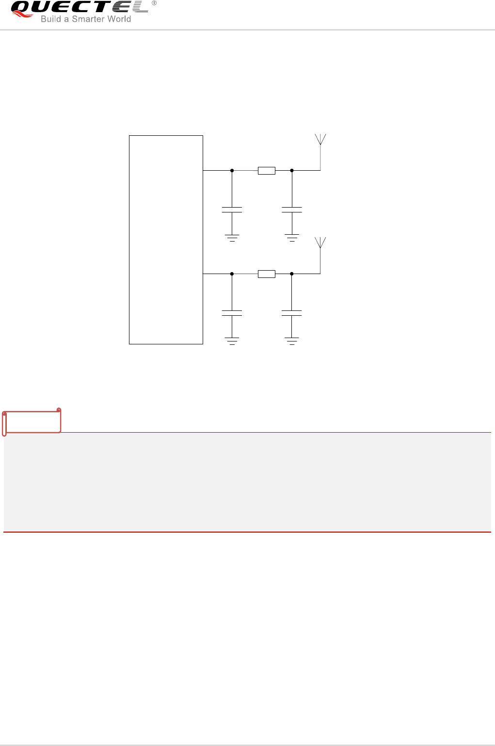
LTE-A Module Series
EG06 Hardware Design
EG06_Hardware_Design 66 / 89
5.1.3. Reference Design of RF Antenna Interface
A reference design of ANT_MAIN and ANT_DIV antenna pads is shown as below. It should reserve a
π-type matching circuit for better RF performance. The capacitors are not mounted by default.
ANT_MAIN
R1 0R
C1
Module Main
Antenna
NM
C2
NM
R2 0R
C3
Diversity
Antenna
NM
C4
NM
ANT_DIV
Figure 32: Reference Circuit of RF Antenna Interface
1. Keep a proper distance between the main antenna and the Rx-diversity antenna to improve the
receiving sensitivity.
2. ANT_DIV function is enabled by default. AT+QCFG="diversity",0 command can be used to disable
receive diversity.
3. Place the π-type matching components (R1/C1/C2 and R2/C3/C4) as close to the antenna as
possible.
5.1.4. Reference Design of RF Layout
For user’s PCB, the characteristic impedance of all RF traces should be controlled as 50Ω. The
impedance of the RF traces is usually determined by the trace width (W), the materials’ dielectric constant,
the distance between signal layer and reference ground (H), and the clearance between RF trace and
ground(S). Microstrip line or coplanar waveguide line is typically used in RF layout for characteristic
impedance control. The following are reference designs of microstrip line or coplanar waveguide line with
different PCB structures.
NOTES
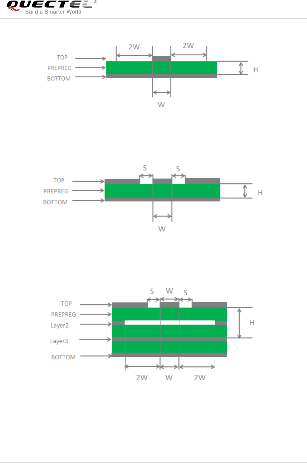
LTE-A Module Series
EG06 Hardware Design
EG06_Hardware_Design 67 / 89
Figure 33: Microstrip Line Design on a 2-layer PCB
Figure 34: Coplanar Waveguide Line Design on a 2-layer PCB
Figure 35: Coplanar Waveguide Line Design on a 4-layer PCB (Layer 3 as Reference Ground)
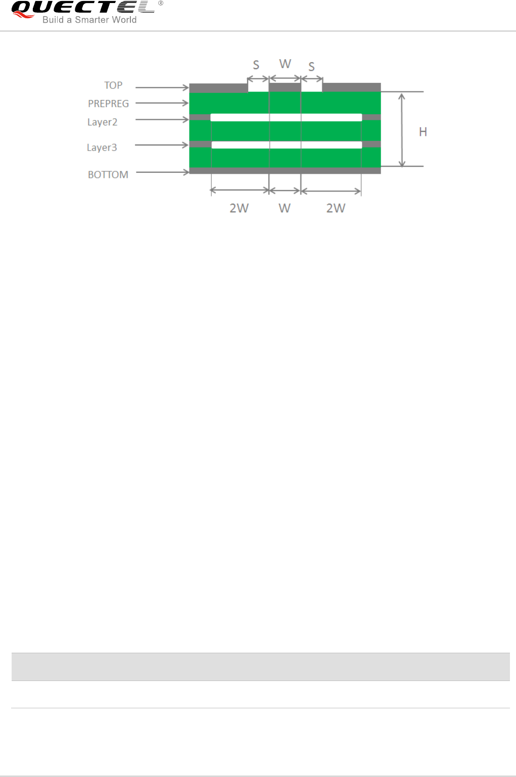
LTE-A Module Series
EG06 Hardware Design
EG06_Hardware_Design 68 / 89
Figure 36: Coplanar Waveguide Line Design on a 4-layer PCB (Layer 4 as Reference Ground)
In order to ensure RF performance and reliability, the following principles should be complied with in RF
layout design:
Use impedance simulation tool to control the characteristic impedance of RF traces as 50Ω.
The GND pins adjacent to RF pins should not be designed as thermal relief pads, and should be fully
connected to ground.
The distance between the RF pins and the RF connector should be as short as possible, and all the
right angle traces should be changed to curved ones.
There should be clearance area under the signal pin of the antenna connector or solder joint.
The reference ground of RF traces should be complete. Meanwhile, adding some ground vias around
RF traces and the reference ground could help to improve RF performance. The distance between
the ground vias and RF traces should be no less than two times the width of RF signal traces (2*W).
For more details about RF layout, please refer to document [5].
5.2. GNSS Antenna Interface
The following tables show pin definition and frequency specification of GNSS antenna interface.
Table 31: Pin Definition of GNSS Antenna Interface
Pin Name
Pin No.
I/O
Description
Comment
ANT_GNSS
119
AI
GNSS antenna pad
50Ω impedance
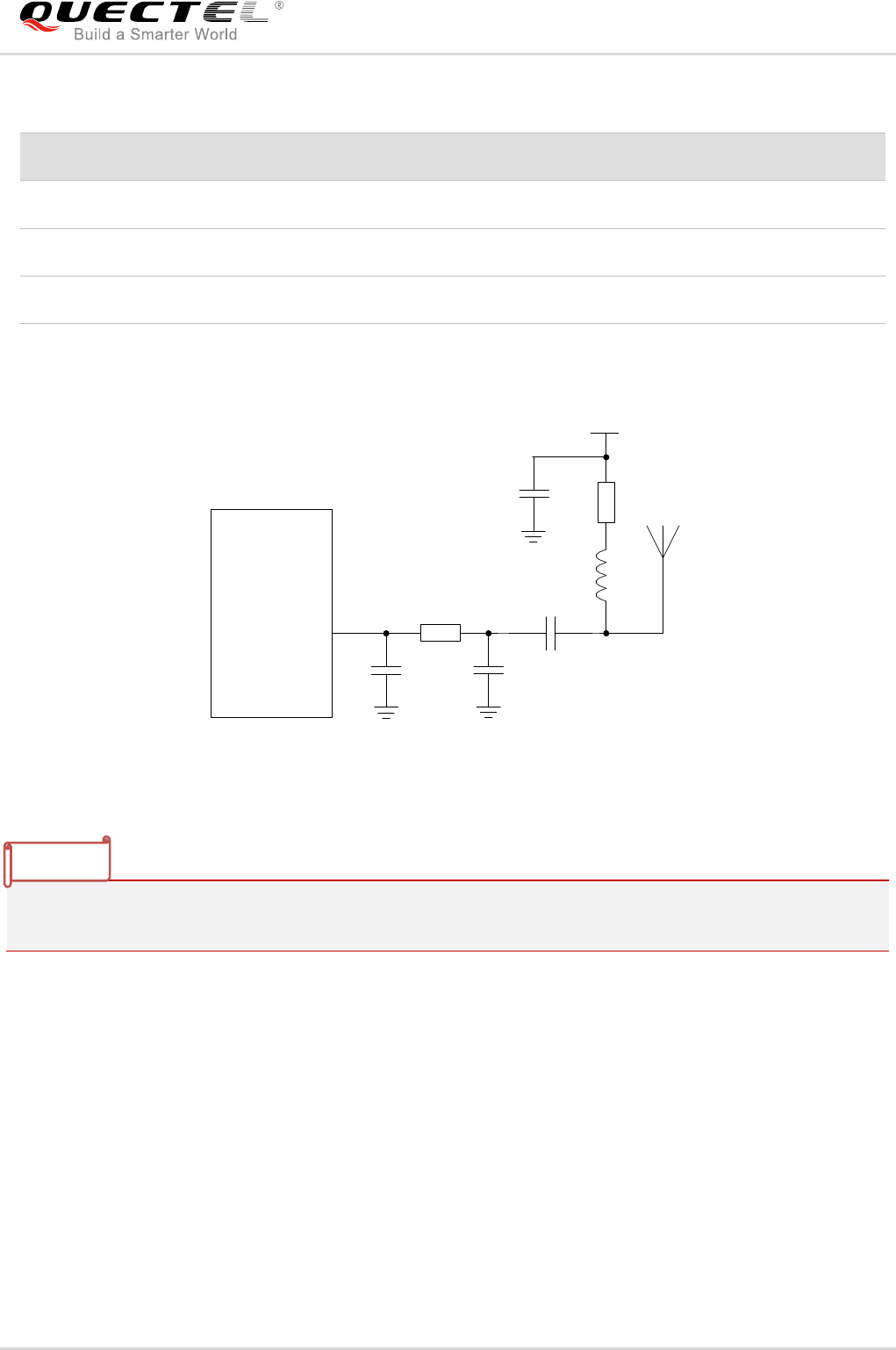
LTE-A Module Series
EG06 Hardware Design
EG06_Hardware_Design 69 / 89
Table 32: GNSS Frequency
A reference design of GNSS antenna is shown as below.
GNSS
Antenna
VDD
Module
ANT_GNSS
47nH
10R
0.1uF
0R
NM NM
100pF
Figure 37: Reference Circuit of GNSS Antenna
1. An external LDO can be selected to supply power according to the active antenna requirement.
2. If the module is designed with a passive antenna, then the VDD circuit is not needed.
5.3. Antenna Installation
5.3.1. Antenna Requirement
The following table shows the requirements on main antenna, Rx-diversity antenna and GNSS antenna.
Type
Frequency
Unit
GPS/Galileo/QZSS
1575.42±1.023
MHz
GLONASS
1597.5~1605.8
MHz
BeiDou
1561.098±2.046
MHz
NOTES
LTE-A Module Series
EG06 Hardware Design
EG06_Hardware_Design 70 / 89
Table 33: Antenna Requirements
Type
Requirements
GNSS1)
Frequency range: 1561MHz ~ 1615MHz
Polarization: RHCP or linear
VSWR: < 2 (Typ.)
Passive antenna gain: > 0dBi
Active antenna noise figure: < 1.5dB
Active antenna gain: > 0dBi
Active antenna embedded LNA gain: < 17dB
WCDMA/LTE
VSWR: ≤ 2
Efficiency: > 30%
Max Input Power: 50W
Input Impedance: 50Ω
Gain: WCDMA Band2: 2dBi ; WCDMA Band4: 2dBi ; WCDMA
Band5: 3dBi ;LTE B2:2dBi; LTE B4:2dBi; LTE B5:3dBi; LTE
B7:2dBi; LTE B12:3dBi; LTE B13:3dBi; LTE B25:2dBi; LTE
B26:3dBi; LTE B30:0dBi; LTE B66:2dBi
Cable insertion loss: < 1dB
(WCDMA B5/B6/B8/B19,
LTE B5/B8/B12/B13/B18/B19/B20/B26/B28/B29/)
Cable insertion loss: < 1.5dB
(WCDMA B1/B2/B3/B4/B9, LTE B1/B2/B3/B4/B21/B25/B66)
Cable insertion loss < 2dB
(LTE B7/B38/B40/B41/B30)
1) It is recommended to use a passive GNSS antenna when LTE B13 or B14 is supported, as the use of
active antenna may generate harmonics which will affect the GNSS performance.
NOTE
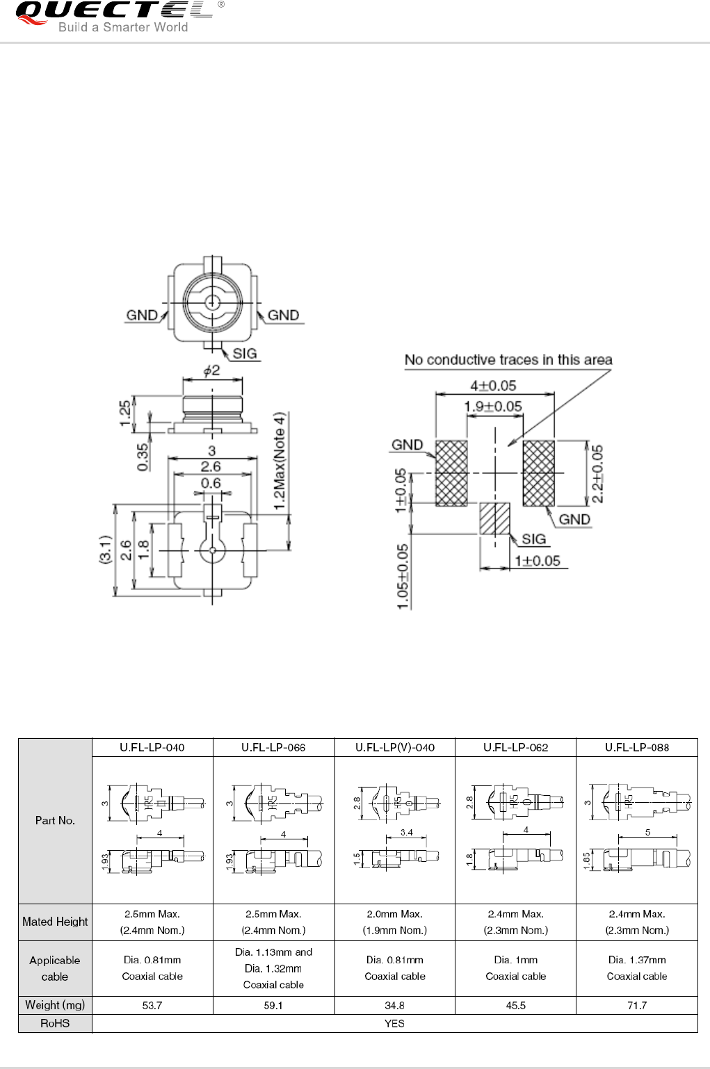
LTE-A Module Series
EG06 Hardware Design
EG06_Hardware_Design 71 / 89
5.3.2. Recommended RF Connector for Antenna Installation
If RF connector is used for antenna connection, it is recommended to use the U.FL-R-SMT connector
provided by Hirose.
Figure 38: Dimensions of the U.FL-R-SMT Connector (Unit: mm)
U.FL-LP serial connector listed in the following figure can be used to match the U.FL-R-SMT.

LTE-A Module Series
EG06 Hardware Design
EG06_Hardware_Design 72 / 89
Figure 39: Mechanicals of U.FL-LP Connectors
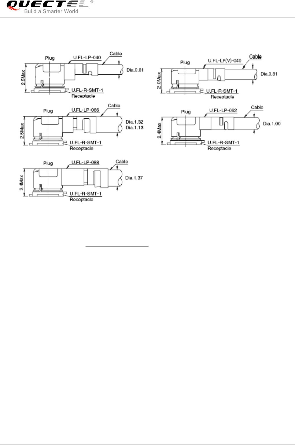
LTE-A Module Series
EG06 Hardware Design
EG06_Hardware_Design 73 / 89
The following figure describes the space factor of mated connector.
Figure 40: Space Factor of Mated Connector (Unit: mm)
For more details, please visit https://www.hirose.com.

LTE-A Module Series
EG06 Hardware Design
EG06_Hardware_Design 74 / 89
6 Electrical, Reliability and Radio
Characteristics
6.1. Absolute Maximum Ratings
Absolute maximum ratings for power supply and voltage on digital and analog pins of the module are
listed in the following table.
Table 34: Absolute Maximum Ratings
Parameter
Min.
Max.
Unit
VBAT_RF/VBAT_BB
-0.3
4.7
V
USB_VBUS
-0.3
5.5
V
Peak Current of VBAT_BB
0
0.8
A
Peak Current of VBAT_RF
0
1
A
Voltage at Digital Pins
-0.3
2.3
V
Voltage at ADC0
0
VBAT_BB
V
Voltage at ADC1
0
VBAT_BB
V
LTE-A Module Series
EG06 Hardware Design
EG06_Hardware_Design 75 / 89
6.2. Power Supply Ratings
Table 35: The Module Power Supply Ratings
6.3. Operation and Storage Temperatures
The operation and storage temperatures are listed in the following table.
Table 36: Operation and Storage Temperatures
1. 1) Within operation temperature range, the module is 3GPP compliant.
2. 2) Within extended temperature range, the module remains the ability to establish and maintain a
voice, SMS, data transmission, emergency call, etc. There is no unrecoverable malfunction. There
are also no effects on radio spectrum and no harm to radio network. Only one or more parameters
like Pout might reduce in their value and exceed the specified tolerances. When the temperature
returns to the normal operating temperature levels, the module will meet 3GPP specifications again.
Parameter
Description
Conditions
Min.
Typ.
Max.
Unit
VBAT
VBAT_BB and
VBAT_RF
The actual input voltages
must stay between the
minimum and maximum
values.
3.3
3.8
4.3
V
USB_VBUS
USB connection
detection
3.0
5.0
5.25
V
Parameter
Min.
Typ.
Max.
Unit
Operation Temperature Range1)
-35
+25
+75
ºC
Extended Operation Range2)
-40
+85
ºC
Storage temperature range:
-40
+90
ºC
NOTES

LTE-A Module Series
EG06 Hardware Design
EG06_Hardware_Design 76 / 89
6.4. Current Consumption
Table 37: EG06-E Current Consumption
Parameter
Description
Conditions
Typ.
Unit
IVBAT
OFF state
Power down
20
uA
Sleep state
AT+CFUN=0 (USB disconnected)
0.8
mA
WCDMA PF=64 (USB disconnected)
1.6
mA
WCDMA PF=128 (USB disconnected)
1.2
mA
WCDMA PF=512 (USB disconnected)
1.0
mA
LTE-FDD PF=32 (USB disconnected)
3.3
mA
LTE-FDD PF=64 (USB disconnected)
2.1
mA
LTE-FDD PF=128 (USB disconnected)
1.5
mA
LTE-TDD PF=32 (USB disconnected)
3.3
mA
LTE-TDD PF=64 (USB disconnected)
2.1
mA
LTE-TDD PF=128 (USB disconnected)
1.5
mA
Idle state
WCDMA PF=64 (USB disconnected)
18
mA
WCDMA PF=64 (USB connected)
29
mA
LTE-FDD PF=64 (USB disconnected)
18
mA
LTE-FDD PF=64 (USB connected)
28
mA
LTE-TDD PF=64 (USB disconnected)
18
mA
LTE-TDD PF=64 (USB connected)
28
mA
WCDMA data
transfer
(GNSS OFF)
WCDMA B1 HSDPA CH10700 @22.7dBm
445
mA
WCDMA B1 HSUPA CH10700 @22.2dBm
450
mA
WCDMA B3 HSDPA CH1338 @22.8dBm
627
mA
WCDMA B3 HSUPA CH1338 @22.3dBm
635
mA
WCDMA B5 HSDPA CH4407 @22.7dBm
540
mA

LTE-A Module Series
EG06 Hardware Design
EG06_Hardware_Design 77 / 89
WCDMA B5 HSUPA CH4407 @22.3dBm
549
mA
WCDMA B8 HSDPA CH3012 @22.6dBm
550
mA
WCDMA B8 HSUPA CH3012 @22.4dBm
560
mA
LTE data
transfer
(GNSS OFF)
LTE-FDD B1 CH300 @23.5dBm
587
mA
LTE-FDD B3 CH1575 @23.7dBm
790
mA
LTE-FDD B5 CH2525 @22.7dBm
532
mA
LTE-FDD B7 CH3100 @23.48dBm
803.2
mA
LTE-FDD B8 CH3625 @23.83dBm
616.9
mA
LTE-FDD B20 CH6300 @23.05dBm
639.5
mA
LTE-FDD B28 CH27460 @23.01dBm
711
mA
LTE-TDD B38 CH38000 @23.88dBm
383.4
mA
LTE-TDD B40 CH39150 @23.67dBm
341.3
mA
LTE-TDD B41 CH40740 @23.88dBm
375.3
mA
2×CA data
transfer
LTE-FDD B1+B1 @21.05dBm
618.7
mA
LTE-FDD B1+B5 @21.07dBm
769.9
mA
LTE-FDD B1+B8 @21.91dBm
619.1
mA
LTE-FDD B1+B20 @20.91dBm
633
mA
LTE-FDD B1+B28 @21.09dBm
746.8
mA
LTE-FDD B3+B5 @21.18dBm
751
mA
LTE-FDD B3+B7 @21.1dBm
789.1
mA
LTE-FDD B3+B8 @21.2dBm
748.2
mA
LTE-FDD B3+B20 @21.16dBm
779.3
mA
LTE-FDD B3+B28 @21.12dBm
786.7
mA
LTE-FDD B7+B5 @21.29dBm
848.3
mA
LTE-FDD B7+B7 @21.33dBm
834.9
mA
LTE-FDD B7+B8 @21.3dBm
852.3
mA
LTE-FDD B7+B20 @21.32dBm
885.9
mA

LTE-A Module Series
EG06 Hardware Design
EG06_Hardware_Design 78 / 89
6.5. RF Output Power
The following table shows the RF output power of EG06 module.
Table 38: RF Output Power
6.6. RF Receiving Sensitivity
The following tables show conducted RF receiving sensitivity of EG06 series module.
LTE-FDD B7+B28 @21.33dBm
881.7
mA
LTE-FDD B5+B32 @20.91dBm
663.4
mA
LTE-FDD B8+B32 @20.88dBm
680
mA
LTE-FDD B20+B32 @20.88dBm
693
mA
LTE-FDD B28+B32 @21.1dBm
777.6
mA
LTE-TDD B38+B38 @21.3dBm
400.5
mA
LTE-TDD B40+B40 @20.99dBm
369.3
mA
LTE-TDD B41+B41 @21.25dBm
403.9
mA
WCDMA
voice call
WCDMA B1 CH10700 @22.83dBm
450.3
mA
WCDMA B3 CH1338 @22.97dBm
650.3
mA
WCDMA B5 CH4407 @22.75dBm
556.3
mA
WCDMA B8 CH3012 @22.89dBm
568
mA
Frequency
Max.
Min.
WCDMA bands
24dBm+1/-3dB
<-50dBm
LTE FDD bands
23dBm±2dB
<-40dBm
LTE TDD bands
23dBm±2dB
<-40dBm

LTE-A Module Series
EG06 Hardware Design
EG06_Hardware_Design 79 / 89
Table 39: EG06-E Conducted RF Receiving Sensitivity
1) SIMO is a smart antenna technology that uses a single antenna at the transmitter side and two
antennas at the receiver side, which can improve Rx performance.
6.7. Electrostatic Discharge
The module is not protected against electrostatics discharge (ESD) in general. Consequently, it is subject
to ESD handling precautions that typically apply to ESD sensitive components. Proper ESD handling and
packaging procedures must be applied throughout the processing, handling and operation of any
application that incorporates the module.
The following table shows the module electrostatic discharge characteristics.
Frequency
Primary
Diversity
SIMO1)
3GPP (SIMO)
WCDMA B1
-109.5dBm
/
/
-106.7dBm
WCDMA B3
-109.5dBm
/
/
-103.7dBm
WCDMA B5
-109.0dBm
/
/
-104.7dBm
WCDMA B8
-110.5dBm
/
/
-103.7dBm
LTE-FDD B1 (10M)
-97.2dBm
-98.8dBm
-101.5dBm
-96.3dBm
LTE-FDD B3 (10M)
-98.5dBm
-97.5dBm
-101.5dBm
-93.3dBm
LTE-FDD B5 (10M)
-96.6dBm
-98.9dBm
-101dBm
-94.3dBm
LTE-FDD B7 (10M)
-96.6dBm
-97.8dBm
-99.5dBm
-94.3dBm
LTE-FDD B8 (10M)
-99.5dBm
-98.8dBm
-101.0dBm
-93.3dBm
LTE-FDD B20 (10M)
-98.0dBm
-100.0dBm
-102.7dBm
-93.3dBm
LTE-FDD B28 (10M)
-99.4dBm
-99.7dBm
-102.5dBm
-94.8dBm
LTE-TDD B38 (10M)
-97.2dBm
-96.5dBm
-100.0dBm
-96.3dBm
LTE-TDD B40 (10M)
-98.3dBm
-96.8dBm
-101.0dBm
-96.3dBm
LTE-TDD B41 (10M)
-97.1dBm
-96.2dBm
-99.2dBm
-94.3dBm
NOTE

LTE-A Module Series
EG06 Hardware Design
EG06_Hardware_Design 80 / 89
Table 40: Electrostatic Discharge Characteristics
6.8. Thermal Consideration
In order to achieve better performance of the module, it is recommended to comply with the following
principles for thermal consideration:
On customers’ PCB design, please keep placement of the module away from heating sources,
especially high power components such as ARM processor, audio power amplifier, power supply,
etc.
Do not place components on the opposite side of the PCB area where the module is mounted and do
not fill that area with copper in order to facilitate adding of heatsink when necessary.
The reference ground of the area where the module is mounted should be complete, and add ground
vias as many as possible for better heat dissipation.
Make sure the ground pads of the module and PCB are fully connected.
According to customers’ application demands, the heatsink can be mounted on the top of the module,
or the opposite side of the PCB area where the module is mounted, or both of them.
The heatsink should be designed with as many fins as possible to increase heat dissipation area.
Meanwhile, a thermal pad with high thermal conductivity should be used between the heatsink and
module/PCB.
The following shows two kinds of heatsink designs for reference and customers can choose one or both
of them according to their application structure.
Tested Points
Contact Discharge
Air Discharge
Unit
VBAT, GND
±5
±1 0
kV
Antenna Interfaces
±4
±8
kV
Other Interfaces
±0.5
±1
kV
LTE-A Module Series
EG06 Hardware Design
EG06_Hardware_Design 81 / 89
Heatsink
EG06 Module
Application Board Application Board
Heatsink
Thermal Pad
Shielding Cover
Figure 41: Referenced Heatsink Design (Heatsink at the Top of the Module)
Thermal Pad
Heatsink
Application Board Application Board
Heatsink
Thermal Pad
EG06 Module
Shielding Cover
Figure 42: Referenced Heatsink Design (Heatsink at the Backside of Customers’ PCB)
1. Make sure that customers’ PCB design provides sufficient cooling for the module: proper mounting,
heatsinks, and active cooling may be required depending on the integrated application.
2. In order to protect the components from damage, the thermal design should be maximally optimized
to make sure the module’s internal temperature always maintains below 105°C . Customers can
execute AT+QTEMP command to get the module’s internal temperature.
NOTES
LTE-A Module Series
EG06 Hardware Design
EG06_Hardware_Design 82 / 89
7 Mechanical Dimensions
This chapter describes the mechanical dimensions of the module. All dimensions are measured in mm,
and the tolerances for dimensions without tolerance values are ±0.05mm.
7.1. Mechanical Dimensions of the Module
Figure 43: Module Top and Side Dimensions
LTE-A Module Series
EG06 Hardware Design
EG06_Hardware_Design 83 / 89
Figure 44: Module Bottom Dimensions (Top View)
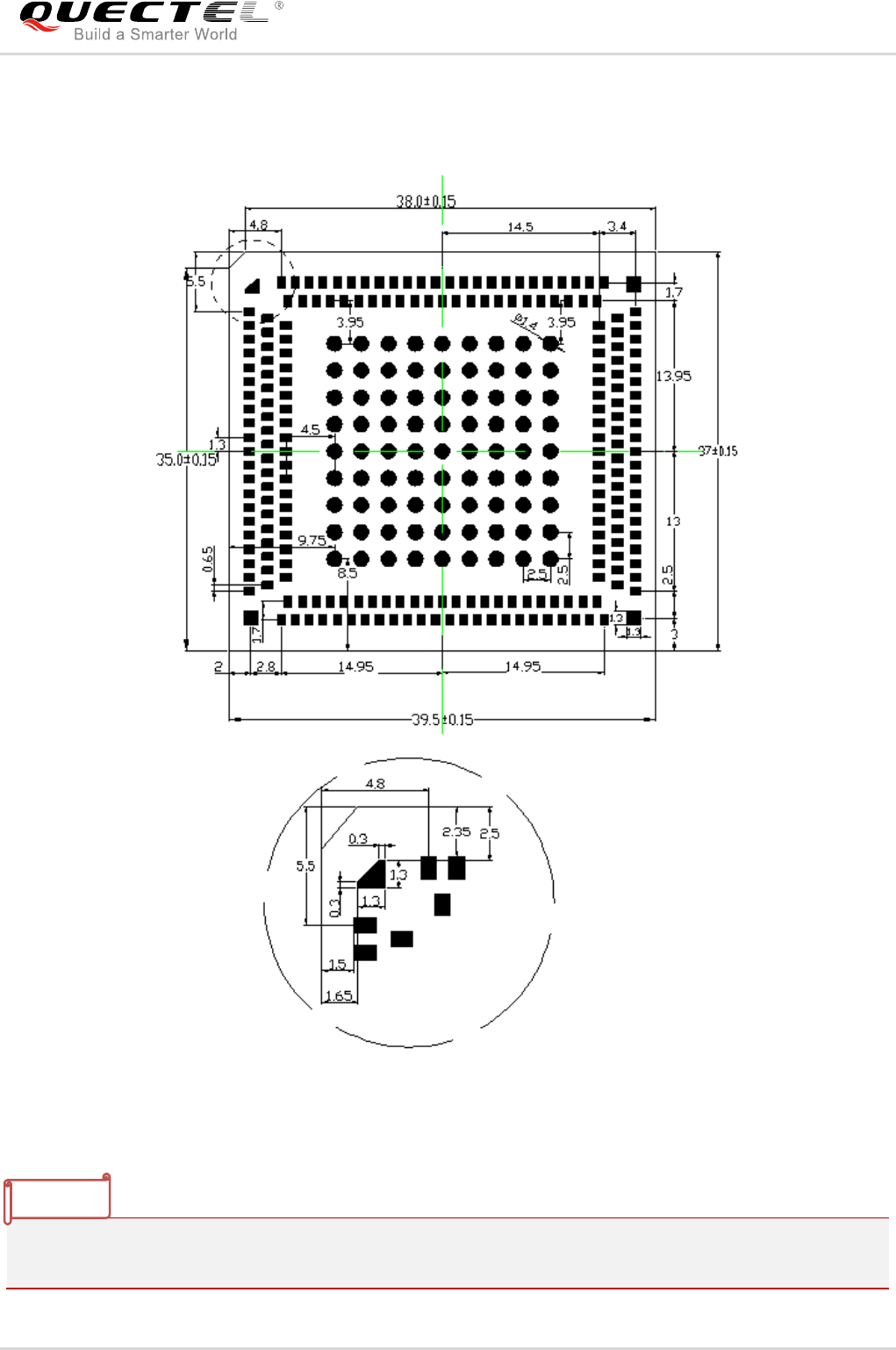
LTE-A Module Series
EG06 Hardware Design
EG06_Hardware_Design 84 / 89
7.2. Recommended Footprint
Figure 45: Recommended Footprint (Top View)
For easy maintenance of the module, please keep about 3mm between the module and other
components in the host PCB.
NOTE
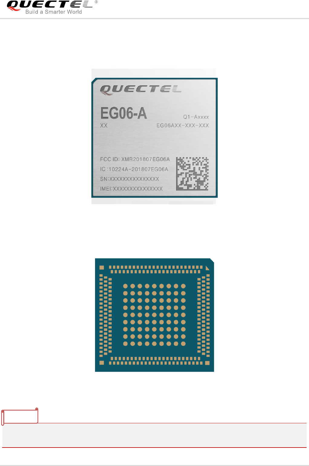
LTE-A Module Series
EG06 Hardware Design
EG06_Hardware_Design 85 / 89
7.3. Design Effect Drawings of the Module
Figure 46: Top View of the Module
Figure 47: Bottom View of the Module
These are design effect drawings of EG06 module. For more accurate pictures, please refer to the
module that you get from Quectel.
NOTE
LTE-A Module Series
EG06 Hardware Design
EG06_Hardware_Design 86 / 89
8 Storage, Manufacturing and
Packaging
8.1. Storage
EG06 is stored in a vacuum-sealed bag. It is rated at MSL 3, and its storage restrictions are listed below.
1. Shelf life in vacuum-sealed bag: 12 months at <40ºC/90%RH.
2. After the vacuum-sealed bag is opened, devices that will be subjected to reflow soldering or other
high temperature processes must be:
Mounted within 168 hours at the factory environment of ≤30ºC/60%RH.
Stored at <10% RH.
3. Devices require baking before mounting, if any circumstance below occurs:
When the ambient temperature is 23ºC±5ºC and the humidity indicator card shows the humidity
is >10% before opening the vacuum-sealed bag.
Device mounting cannot be finished within 168 hours at factory conditions of ≤30ºC/60%RH.
Stored at >10% RH after the vacuum-sealed bag is opened.
4. If baking is required, devices may be baked for 8 hours at 120ºC±5ºC.
As the plastic container cannot be subjected to high temperature, it should be removed from devices
before high temperature (120ºC) baking. If shorter baking time is desired, please refer to
IPC/JEDECJ-STD-033 for baking procedure.
NOTE
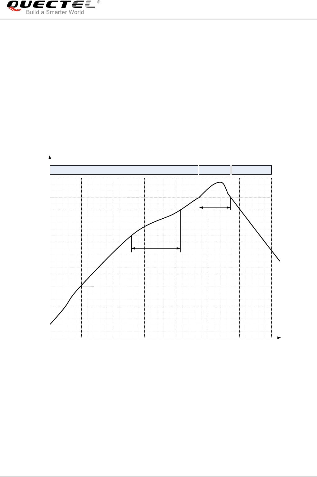
LTE-A Module Series
EG06 Hardware Design
EG06_Hardware_Design 87 / 89
8.2. Manufacturing and Soldering
Push the squeegee to apply the solder paste on the surface of stencil, thus making the paste fill the
stencil openings and then penetrate to the PCB. The force on the squeegee should be adjusted properly
so as to produce a clean stencil surface on a single pass. To ensure the module soldering quality, the
thickness of stencil for the module should be 0.18mm. For more details, please refer to document [3].
It is suggested that the peak reflow temperature is 235ºC ~ 245ºC (for SnAg3.0Cu0.5 alloy). The absolute
max reflow temperature is 260ºC. To avoid damage to the module caused by repeated heating, it is
suggested that the module should be mounted after reflow soldering for the other side of PCB has been
completed. Recommended reflow soldering thermal profile is shown below:
Time
50 100 150 200 250 300
50
100
150
200
250
160ºC
200ºC
217
0
70s~120s
40s~60s
Between 1~3ºC/s
Preheat Heating Cooling
ºC
s
Liquids Temperature
Temperature
Figure 48: Reflow Soldering Thermal Profile
8.3. Packaging
EG06 is packaged in tape and reel carriers. One reel is 10.56 meters long and contains 200 modules. The
figures below show the packaging details, measured in mm.
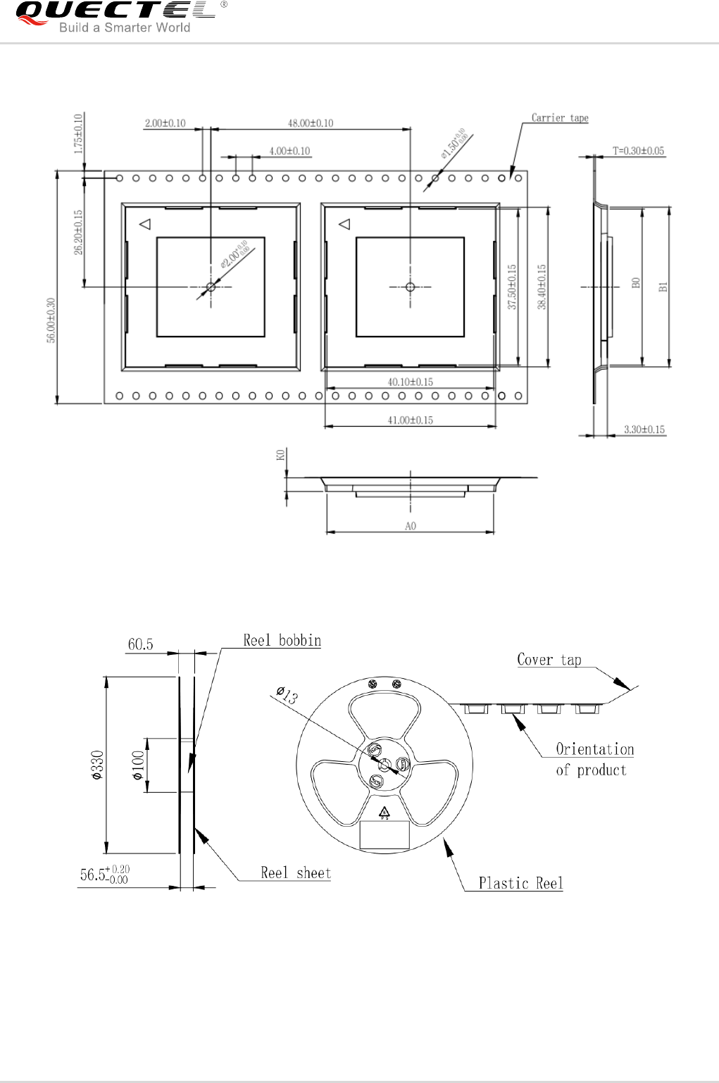
LTE-A Module Series
EG06 Hardware Design
EG06_Hardware_Design 88 / 89
Figure 49: Tape Specifications
Figure 50: Reel Specifications

LTE Module Sires
EG06Hardware Design
EG06_Hardware_Design 89 / 89
9 Appendix A References
Table 41: Related Documents
Table 42: Terms and Abbreviations
SN
Document Name
Remark
[1]
Quectel_Ex06_AT_Commands_Manual
EG06 AT Commands Manual
[2]
Quectel_Ex06_GNSS_AT_Commands_
Manual
EG06 GNSS AT Commands Manual
[3]
Quectel_Module_Secondary_SMT_User_Guide
Module Secondary SMT User Guide
[4]
Quectel_EG06_Reference_Design
EG06 Reference Design
[5]
Quectel_RF_Layout_Application_Note
RF Layout Application Note
Abbreviation
Description
AMR
Adaptive Multi-rate
bps
Bits Per Second
CHAP
Challenge Handshake Authentication Protocol
CS
Coding Scheme
CSD
Circuit Switched Data
CTS
Clear To Send
DC-HSPA+
Dual-carrier High Speed Packet Access
DFOTA
Delta Firmware Upgrade Over The Air
DL
Downlink
DTR
Data Terminal Ready

LTE Module Sires
EG06Hardware Design
EG06_Hardware_Design 90 / 89
DTX
Discontinuous Transmission
EFR
Enhanced Full Rate
ESD
Electrostatic Discharge
FDD
Frequency Division Duplex
FR
Full Rate
GLONASS
GLObalnaya NAvigatsionnaya Sputnikovaya Sistema, the Russian Global
Navigation Satellite System
GMSK
Gaussian Minimum Shift Keying
GNSS
Global Navigation Satellite System
GPS
Global Positioning System
HR
Half Rate
HSPA
High Speed Packet Access
HSDPA
High Speed Downlink Packet Access
HSUPA
High Speed Uplink Packet Access
I/O
Input/Output
Inorm
Normal Current
LED
Light Emitting Diode
LNA
Low Noise Amplifier
LTE
Long Term Evolution
MIMO
Multiple Input Multiple Output
MO
Mobile Originated
MS
Mobile Station
MT
Mobile Terminated
PAP
Password Authentication Protocol
PCB
Printed Circuit Board
PDU
Protocol Data Unit

LTE Module Sires
EG06Hardware Design
EG06_Hardware_Design 91 / 89
PPP
Point-to-Point Protocol
QAM
Quadrature Amplitude Modulation
QPSK
Quadrature Phase Shift Keying
RF
Radio Frequency
RHCP
Right Hand Circularly Polarized
Rx
Receive
SGMII
Serial Gigabit Media Independent Interface
SIMO
Single Input Multiple Output
SMS
Short Message Service
TDD
Time Division Duplexing
TDMA
Time Division Multiple Access
TD-SCDMA
Time Division-Synchronous Code Division Multiple Access
Tx
Transmitting Direction
UL
Uplink
UMTS
Universal Mobile Telecommunications System
URC
Unsolicited Result Code
(U)SIM
Universal Subscriber Identity Module
Vmax
Maximum Voltage Value
Vnorm
Normal Voltage Value
Vmin
Minimum Voltage Value
VIHmax
Maximum Input High Level Voltage Value
VIHmin
Minimum Input High Level Voltage Value
VILmax
Maximum Input Low Level Voltage Value
VILmin
Minimum Input Low Level Voltage Value
VImax
Absolute Maximum Input Voltage Value

LTE Module Sires
EG06Hardware Design
EG06_Hardware_Design 92 / 89
VImin
Absolute Minimum Input Voltage Value
VOHmax
Maximum Output High Level Voltage Value
VOHmin
Minimum Output High Level Voltage Value
VOLmax
Maximum Output Low Level Voltage Value
VOLmin
Minimum Output Low Level Voltage Value
VSWR
Voltage Standing Wave Ratio
WCDMA
Wideband Code Division Multiple Access
WLAN
Wireless Local Area Network

LTE Module Sires
EG06Hardware Design
EG06_Hardware_Design 93 / 89
10 IC & FCC Requirement
10.1. FCC Regulations:
This device complies with part 15 of the FCC Rules. Operation is subject to the following two
conditions: (1) This device may not cause harmful interference, and (2) This device must accept any
interference received, including interference that may cause undesired operation.
This device has been tested and found to comply with the limits for a Class B digital device , pursuant
to Part 15 of the FCC Rules. These limits are designed to provide reasonable protection against
harmful interference in a residential installation. This equipment generates, uses and can radiated
radio frequency energy and, if not installed and used in accordance with the instructions, may cause
harmful interference to radio communications. However, there is no guarantee that interference will
not occur in a particular installation If this equipment does cause harmful interference to radio or
television reception, which can be determined by turning the equipment off and on, the user is
encouraged to try to correct the interference by one or more of the following measures:
-Reorient or relocate the receiving antenna.
-Increase the separation between the equipment and receiver.
-Connect the equipment into an outlet on a circuit different from that to which the receiver is
connected.
-Consult the dealer or an experienced radio/TV technician for help.
Caution: Changes or modifications not expressly approved by the party responsible for compliance
could void the user‘s authority to operate the equipment.
10.2. RF Exposure Information
This device complies with FCC radiation exposure limits set forth for an uncontrolled environment. In
order to avoid the possibility of exceeding the FCC radio frequency exposure limits, human proximity
to the antenna shall not be less than 20cm (8 inches) during normal operation.
10.3. ISED Notice
This device complies with Innovation, Science and Economic Development Canada license-exempt
RSS standard(s). Operation is subject to the following two conditions:
(1) this device may not cause interference, and
(2) this device must accept any interference, including interference that may cause undesired
operation of the device.

LTE Module Sires
EG06Hardware Design
EG06_Hardware_Design 94 / 89
Le présent appareil est conforme aux CNR Innovation, Sciences et Développement économique
Canada applicables aux appareils radio exempts de licence. L'exploitation est autorisée aux deux
conditions suivantes:
(1) l'appareil ne doit pas produire de brouillage, et
(2) l'utilisateur de l'appareil doit accepter tout brouillage radioélectrique subi, même si le brouillage
est susceptible d'en
This Class B digital apparatus complies with Canadian ICES-003.
Cet appareil numérique de la classe B est conforme à la norme NMB-003 du Canada.
10.4. ISED Radiation Exposure Statement
This device complies with RSS-102 radiation exposure limits set forth for an uncontrolled
environment. In order to avoid the possibility of exceeding the ISED radio frequency exposure limits,
human proximity to the antenna shall not be less than 20cm (8 inches) during normal operation.
Cet appareil est conforme aux limites d'exposition aux rayonnements de la CNR-102 définies pour
un environnement non contrôlé. Afin d'éviter la possibilité de dépasser les limites d'exposition aux
fréquences radio de la CNR-102, la proximité humaine à l'antenne ne doit pas être inférieure à 20 cm
(8 pouces) pendant le fonctionnement normal.
10.5. IMPORTANT NOTE:
This module is intended for OEM integrator. The OEM integrator is still responsible for the FCC
compliance requirement of the end product, which integrates this module. 20cm minimum distance
has to be able to be maintained between the antenna and the users for the host this module is
integrated into. Under such configuration, the FCC radiation exposure limits set forth for an
population/uncontrolled environment can be satisfied.
Any changes or modifications not expressly approved by the manufacturer could void the user's
authority to operate this equipment.
10.6. USERS MANUAL OF THE END PRODUCT:
In the users manual of the end product, the end user has to be informed to keep at least 20cm
separation with the antenna while this end product is installed and operated. The end user has to be
informed that the FCC radio-frequency exposure guidelines for an uncontrolled environment can be
satisfied. The end user has to also be informed that any changes or modifications not expressly
approved by the manufacturer could void the user's authority to operate this equipment. If the size of
the end product is smaller than 8x10cm, then additional FCC part 15.19 statement is required to be
available in the users manual: This device complies with Part 15 of FCC rules. Operation is subject to

LTE Module Sires
EG06Hardware Design
EG06_Hardware_Design 95 / 89
the following two conditions: (1) this device may not cause harmful interference and (2) this device
must accept any interference received, including interference that may cause undesired operation.
10.7. LABEL OF THE END PRODUCT:
The final end product must be labeled in a visible area with the following " Contains Transmitter
Module FCC ID: XMR201807EG06A. If the size of the end product is larger than 8x10cm, then the
following FCC part 15.19 statement has to also be available on the label: This device complies with
Part 15 of FCC rules.
Operation is subject to the following two conditions: (1) this device may not cause harmful
interference and (2) this device must accept any interference received, including interference that
may cause undesired operation.
The Innovation, Science and Economic Development Canada certification label of a module shall be
clearly visible at all times when installed in the host device; otherwise, the host device must be
labeled to display the Innovation, Science and Economic Development Canada certification number
for the module, preceded by the words “Contains transmitter module IC: 10224A-201807EG06A.