RELM Communications RPV516A VHF FM Transceiver User Manual
RELM Communications Inc VHF FM Transceiver Users Manual
Contents
- 1. Users Manual
- 2. Revised Manual 121901
- 3. Revised Manual 010402
Users Manual
PRELIMINARY
PRELIMINARY PRELIMINARY
PRELIMINARY –
––
–
Owner’s Manual
Owner’s ManualOwner’s Manual
Owner’s Manual
The following statement will be added here
in the Owner’s Manual.
FCC REQUIREMENTS
FCC REQUIREMENTSFCC REQUIREMENTS
FCC REQUIREMENTS
The RPV516A portable radio must be
properly licensed by the Federal
Communications Commission (FCC) prior to
use. Your local RELM dealer can assist you
in meeting this requirement.
PRELIMINARY
PRELIMINARY PRELIMINARY
PRELIMINARY –
––
–
Owner’s Manual
Owner’s ManualOwner’s Manual
Owner’s Manual
PRELIMINARY
PRELIMINARY PRELIMINARY
PRELIMINARY –
––
–
Owner’s Manual
Owner’s ManualOwner’s Manual
Owner’s Manual
PRELIMINARY
PRELIMINARY PRELIMINARY
PRELIMINARY –
––
–
Owner’s Manual
Owner’s ManualOwner’s Manual
Owner’s Manual
PRELIMINARY
PRELIMINARY PRELIMINARY
PRELIMINARY –
––
–
Owner’s Manual
Owner’s ManualOwner’s Manual
Owner’s Manual
PRELIMINARY
PRELIMINARY PRELIMINARY
PRELIMINARY –
––
–
Service
ServiceService
Service Manual
Manual Manual
Manual
DR• CHKD• APPD• 24
Catalog
CatalogCatalog
Catalog
General
GeneralGeneral
General
P2
P2P2
P2
Specifications
SpecificationsSpecifications
Specifications
P3
P3 P3
P3
Mode Combination P4
Mode Combination P4Mode Combination P4
Mode Combination P4
Circuit Description P5
Circuit Description P5Circuit Description P5
Circuit Description P5
Softwar
SoftwarSoftwar
Software Description
e Descriptione Description
e Description
P10
P10 P10
P10
Test Description P15
Test Description P15Test Description P15
Test Description P15
RPV516A
RPV516ARPV516A
RPV516A Circuit Diagram
Circuit Diagram Circuit Diagram
Circuit Diagram
RPV516A
RPV516ARPV516A
RPV516APCB Component Diagram
PCB Component DiagramPCB Component Diagram
PCB Component Diagram(
((
(Two layers Mech 1 and
Two layers Mech 1 and Two layers Mech 1 and
Two layers Mech 1 and
Mech 2 in PCB
Mech 2 in PCBMech 2 in PCB
Mech 2 in PCB)
))
)
PRELIMINARY
PRELIMINARY PRELIMINARY
PRELIMINARY –
––
–
Service
ServiceService
Service Manual
Manual Manual
Manual
DR• CHKD• APPD• 25
General
GeneralGeneral
General
This manual is intended for use by experienced technicians familiar with
similar types of commercial grade communications equipment. It contains
main required service information and data for the equipment.
The following precautions are recommended for personal safety:
1. DO NOT transmit until all RF connectors are verified secure and any
open connectors are properly terminated.
2. SHUT OFF and DO NOT operate this equipment near electrical
blasting caps or in an explosive atmosphere.
3. This equipment should be maintained by qualified technicians only.

PRELIMINARY
PRELIMINARY PRELIMINARY
PRELIMINARY –
––
–
Service
ServiceService
Service Manual
Manual Manual
Manual
DR• CHKD• APPD• 26
Main technical specifications
General RPV516A(1) RPV516A(2)
Frequency 136MHz~150MHz 150MHz~174MHz
Channel 16
Channel space 25kHz / 12.5kHz
Antenna impedance 50•
Transmitter
impedance 2KΩ
Input voltage 7.2V DC
Frequency stability ±2.5×10⁻⁶
TCXO 12.8MHz
CPU clock Freq 7.3728MHz
Transmitter
Frequency stability ±
2.5×
10-6
Output power 4.0±
0.5W
Operating
sensitivity 12±4mV
Audio distortion ≤5%
Modulation limiting ≤5kHz / 2.5kHz
Bandwidth ≤16 kHz/8kHz
Modulate speciality ≤±3dB
Spurious RF ≤7.5μW
Adjacent power ≤-65 d B / -55dB
Receiver
Reference
sensitivity Precede 0.28•V / 0.35•V
Squelch turnon
sensitivity ≤0.4•V
Audio frequency 500mW
Audio deviation ≤7%
Operating bandwidth ≥│
±
7 kHz│/│±
3.5 kHz│
Audio response ≤+2dB -8dB
First IF Freq 38.85MHz
Second IF Freq 450kHz
Channel restrain ≥-8 d B
Obstruct ≥85d B
Selectivity ≥65 d B / 60dB
Spurious response ≥60 d B
Intermodulation ≥60 d B
PRELIMINARY
PRELIMINARY PRELIMINARY
PRELIMINARY –
––
–
Service
ServiceService
Service Manual
Manual Manual
Manual
DR• CHKD• APPD• 27
Mode combination
1.Mode
User mode: Turn on the power to enter.
PC mode:Set and adjust with PC software or programmer.
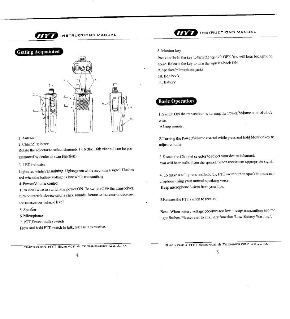
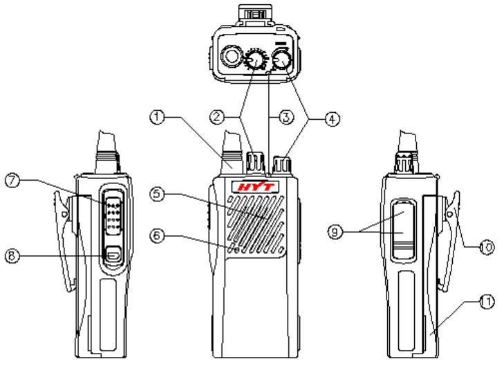
2. Parts description:
•.Antenna
•.Channel (frequency) selector knob
turn the knob to choose channel from 1~16•channel 16 may be set by
distributor as scan channel••
•.LED light
Lights red while transmitting, green while receiving a signal. Flashes red
when the battery voltage is low, while transmitting.
•.Power switch/Volume control
Turn the knob clockwise to switch the transceiver ON, anti-clockwise to turn
off the power till there is a “click” sound , rotate to adjust the volume level.
(5)Speaker
•.Microphone
•.PTT•push to talk•switch
Press the button while transmitting, and release it while receiving.
•.Monitor key
Press it to shut off squelch, noise could be heard, release to connect
squelch.
•.Speaker/microphone jack
•.Belt clip
•.Battery•TB-82•
PRELIMINARY
PRELIMINARY PRELIMINARY
PRELIMINARY –
––
–
Service
ServiceService
Service Manual
Manual Manual
Manual
DR• CHKD• APPD• 28
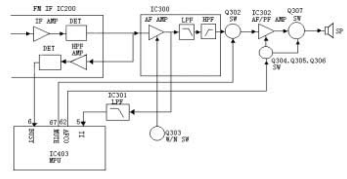
Circuit Description
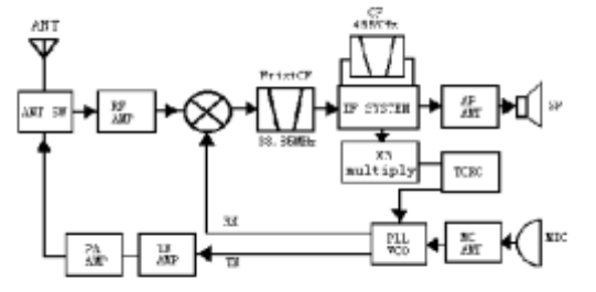
3. Frequency configuration
The receiver utilizes double conversion. The first IF is 38.85MHz and the
second IF is 450KHZ. The first local oscillator signal is supplied from the
PLL circuit.
The PLL circuit in the transmitter generates the necessary frequencies.
Fig.1 shows the frequencies.
Fig1. Frequency configuration
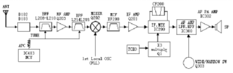
4. Receiver
The receiver is double conversion superheterodyne, designed to
operate in the frequency range of 150-174 MHz (M type), 136——
150MHZ•M2 type••
1) Front-end RF amplifier
An incoming signal from the antenna is applied to an RF
amplifier(Q203) after passing through a transmit/receive switch
circuit(D 102 and D103 are off ) and a band pass filter(L208, L209
and L210). After the signal is amplified(Q203), the signal is filtered
through a band pass filter (L203 and L214) to eliminate unwanted
signals before it is passed to the first mixer. Band pass filters (L208,
L209, L210, L203 and L214) have varactor diodes (D203, D204,
D206, D202 and D201).
The voltage of these diodes are controlled by to track the MPU
(IC403) center frequency of the band pass filter. (See Fig. 2)
PRELIMINARY
PRELIMINARY PRELIMINARY
PRELIMINARY –
––
–
Service
ServiceService
Service Manual
Manual Manual
Manual
DR• CHKD• APPD• 29
Fig. 2. Receiver section configuration
2) First Mixer
The signal from the RF amplifier is heterodyned with the first local
oscillator signal from the PLL frequency synthesizer circuit at the first
mixer (Q202) to create a 38.85 MHz first intermediate frequency (1st
IF) signal. The first IF signal is then fed through two monolithic crystal
filters (MCFs: XF200) to further remove spurious signals.
3) IF amplifier
The first IF signal is amplified by Q201, and then enters IC 200 (FM processing IC). The
signal is heterodyned again with a second local oscillator signal within IC200 to create a
450kHz second IF signal. The second IF signal is then fed through a 450kHz ceramic filter
(CF200) to further eliminate unwanted signals before it is amplified and FM detected in
IC200.
4) AF amplifier
The recovered AF signal obtained from IC200 is amplified by IC300
(1/4), filtered by the IC300 low-pass filter (2/4) and IC300 high-pass
filter (3/4) and (4/4), and de-emphasized by R303 and C306. The AF
signal is then passed through a WIDE/NARROW switch (Q303). The
processed AF signal passes through an AF volume control and is
amplified to a sufficient level to drive a loud speaker by an AF
power amplifier (IC302).
5) Squelch
Part of the AF signal from the IC enters the FM IC again, and the
noise component is amplified and rectified by a filter and an
amplifier to produce a DC voltage corresponding to the noise level.
The DC signal from the FM IC goes to the analog port of the
microprocessor (IC403). IC403 determines whether to output
sounds from the speaker, IC403 sends a high signal to the MUTE and
AFCO lines and turns IC302 on through Q302, Q304, Q305, Q306
and Q307. (See Fig.3)
PRELIMINARY
PRELIMINARY PRELIMINARY
PRELIMINARY –
––
–
Service
ServiceService
Service Manual
Manual Manual
Manual
DR• CHKD• APPD• 30
Fig.3. AF Amplifier and squelch
6) Receiving signaling
QT/DQT
300 Hz and higher audio frequencies of the output signal from IF IC
are cut by a low-pass filter (IC301). The resulting signal enters the
microprocessor (IC403). IC403 determines whether the QT or DQT
matches the preset value, and controls the MUTE and AFCO and the
speaker output sounds according to the squelch results.
3. PLL frequency synthesizer
The PLL circuit generates the first local oscillator signal for reception and
the RF signal for transmission.
2) PLL
The frequency step of the PLL circuit is 5 or 6.25KHz. A 12.8MHz
reference oscillator signal is divided at IC1 by a fixed counter to
produce the 5 or 6.25KHz reference frequency. The voltage controlled
oscillator (VCO) output signal is buffer amplified by Q6, then divided in
IC1 by a dual-module programmable counter. The divided signal is
compared in phase with the 5 or 6.25KHz reference signal in the phase
comparator in IC1. The output signal from the phase comparator is
filtered through a low-pass filter and passed to the VCO to control the
oscillator frequency. (See Fig. 4)
2) VCO
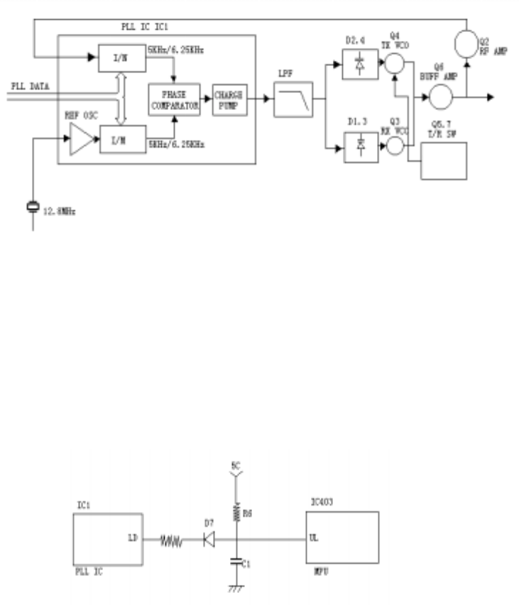
PRELIMINARY
PRELIMINARY PRELIMINARY
PRELIMINARY –
––
–
Service
ServiceService
Service Manual
Manual Manual
Manual
DR• CHKD• APPD• 31
The operating frequency is generated by Q4 in transmit mode and Q3 in receive mode. The
oscillator frequency is controlled by applying the VCO control voltage, obtained from the phase
comparator, to the varactor diodes (D2 and D4 in transmit mode and D1 and D3 in receive mode)
. The T/R pin is set high in receive mode causing Q5 and Q7 to turn Q4 off, and turn Q3 on. The
T/R pin is set low in transmit mode. The outputs from Q3 and Q4 are amplified by Q6 and sent to
the buffer amplifiers.
Fig. 4. PLL circuit
4) UNLOCK DETECTOR
If a pulse signal appears at the LD pin of IC1, an unlock condition
occurs, and the DC voltage obtained from D7, R6, and C1 causes the
voltage applied to the UL pin of the microprocessor to go low. When the
microprocessor detects this condition, the transmitter is disabled,
ignoring the push-to-talk switch input signal. (See Fig. 5)
Fig.5. Unlock detector circuit
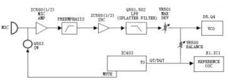
4•Transmitter
1•Transmit audio
The modulation signal from the microphone is amplified by IC500
(1/2), passes through a preemphasis circuit, and amplified by the other
IC500 (1/2) to perform IDC operation. The signal then passes through a low-
pass filter (splatter filter) (Q501 and Q502) and cuts 3kHz and higher
PRELIMINARY
PRELIMINARY PRELIMINARY
PRELIMINARY –
––
–
Service
ServiceService
Service Manual
Manual Manual
Manual
DR• CHKD• APPD• 32
frequencies. The resulting signal goes to the VCO through the VCO
modulation terminal for direct FM modulation. (See Fig. 6)
7) QT/DQT encoder
A necessary signal for QT/DQT encoding is generated by IC403 and FM-
modulated to the PLL reference signal. Since the reference OSC does
not modulate the loop characteristic frequency or higher, modulation is
performed at the VCO side by adjusting the balance. (See Fig. 6)
•6. Transmit audio QT/DQT
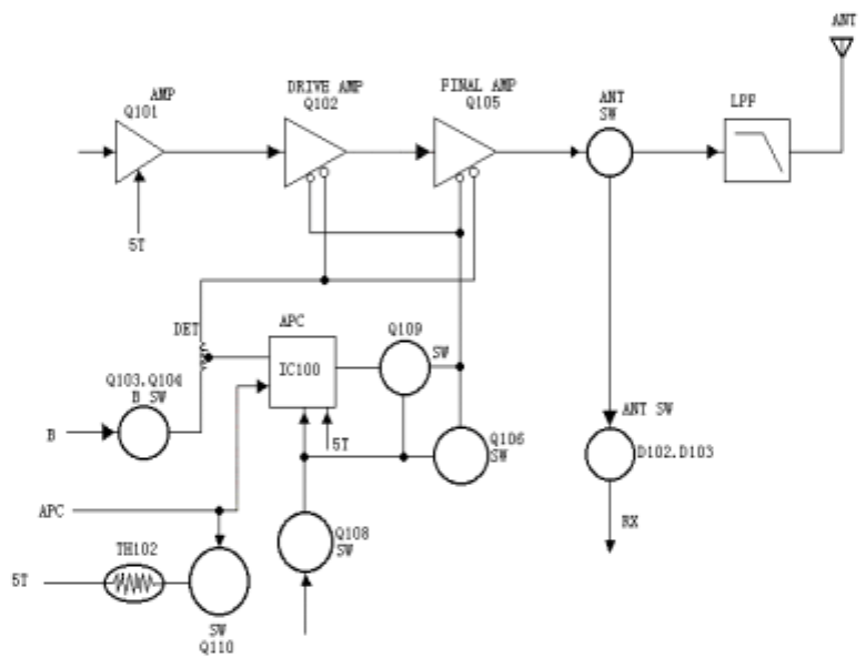
8) VCO and RF amplifier
The transmit signal obtained from the VCO buffer amplifier Q100, is
amplified by Q101. This amplified signal is passed to the power
amplifier, Q102 and Q105, which consists of a 2-stage FET amplifier and
is capable of producing up to 5W of RF power (See Fig. 7)
PRELIMINARY
PRELIMINARY PRELIMINARY
PRELIMINARY –
––
–
Service
ServiceService
Service Manual
Manual Manual
Manual
DR• CHKD• APPD• 33
Fig. 7. APC system
9) ANT switch and LPF
The RF amplifier output signal is passed through a low-pass filter network
and a transmit/receive switching circuit before it is passed to the antenna
terminal. The transmit/receive switching circuit is comprised of D101, D102
and D103. D102 and D103 turned on (conductive ) in transmit mode and
off (isolated) in receive mode.
10) APC
The automatic power control (APC) circuit stabilizes the transmitter output
power at a predetermined level by sensing the drain current of the final
amplifier Field Effect Transistor (FET). The voltage obtained from the
above drain current with a reference voltage which is set using the
microprocessor. An APC voltage proportional to the difference between
the sensed voltage and the reference voltage appears at the output of
IC100 (1/2). This output voltage controls the gate of the FET power
amplifier, which keeps the transmitter output power can be varied by
the microprocessor which in turn changes the reference voltage and
hence , the output power.
11) Terminal protection circuit
When the thermistor (TH102) reaches about 80℃•the protection circuit
PRELIMINARY
PRELIMINARY PRELIMINARY
PRELIMINARY –
––
–
Service
ServiceService
Service Manual
Manual Manual
Manual
DR• CHKD• APPD• 34
turns on Q110 to protect transmitting final amplifier (Q107).
5•Power supply
A 5V reference power supply [5M] for the control circuit is derived from an
internal battery. This reference is used to provide a 5V supply in transmit
mode [5T] ,a 5V supply in receive mode [5R] , and a 5V•supply common in
both modes [5C] based on the control signal sent from the microprocessor.
6•Control system
The IC403 CPU operates at 7.37MHZ. This oscillator has a circuit that shifts
the frequency according to the EEPROM data.
PRELIMINARY
PRELIMINARY PRELIMINARY
PRELIMINARY –
––
–
Service
ServiceService
Service Manual
Manual Manual
Manual
DR• CHKD• APPD• 35
RPV516A
RPV516ARPV516A
RPV516A/TC
/TC/TC
/TC368
368368
368 software specifications
software specifications software specifications
software specifications
一. Specifications•
1. Use mechanical knob to choose from 16 channels.
Frequency
VHF:136~150MHz•VHF:150~174MHz•UHF:400~420MHz•UHF:450~47
0MHz
2. Monitor
3. Auto power saving
4. Audio alarm
5. Auto squelch control (0~9 level)•
6. Timing
7. Channel space 25KHz/12.5KHz(Wide/Narrow)
8. CTCSS&DQT encode
9. CTCSS &DQT decode
10. Busy channel lock
11. Clock frequency deviation
12. Scan
13. PC mode
14. PC modifying mode
15. Wire clone
16. Manual modifying mode
二. Description•
1. User mode•general radio mode
2. PC mode•
Make settings through external programmer or PC program software•
(1) Receive frequency &transmit frequency
(2) Receive signaling& Transmit signaling
(3) Lock busy channel
(4) Clock frequency deviation
(5) Timing
(6) Squelch level selectivity
(7) Power saving
(8) Audio Alarm
(9) Channel space 25KHz/12.5KHz(Wide/Narrow)
(10) Monitor mode
(11) Scan mode
PRELIMINARY
PRELIMINARY PRELIMINARY
PRELIMINARY –
––
–
Service
ServiceService
Service Manual
Manual Manual
Manual
DR• CHKD• APPD• 36
(12) Reset scan mode
(13) Scan priority
3. PC modify mode•
Make settings through external programmer or PC program software:
(1)
Frequency stability
(2)
RF power
(3)
Low power alarm
(4) Squelch•level 9&3•
(5) CTCSS deviation•Wide/Narrow••
(6)
DQT deviation•Wide/Narrow••
(7)
Receive sensitivity•low•medium•high•
4. Wire Clone:
Press MONI to turn on the power , enter wire clone mode 2 seconds
later, press PTT,
Begin cloning while red lights, finish while light goes out.
5. Mode setting:
• Short cut the SELF on PCB, and turn on the power till “BEEP”.
• Set channel selector knob to corresponding place according to
the model•1-16•
• Press [MONI]•then press [PTT], to set the channel, channel data and
initial data.
• Turn off the power, disconnect SELF on PCB to end mode settings.
Eg. RPV516A•2•, its serial number is 2, to initialize: short cut SELF on
PCB to turn on
The power, set channel selector knob at CH2, press MONI, then press
PTT, the initial data of 1-4 channel can be found in the diagram,
serial number 2. Reset data to initial data. The receive and transmit
frequency of channel 5-14 are the same with channel 1, signals are
channel5, 10•67.0Hz•6,11•151.4Hz•7,12•250.3Hz•8,13•423•DQT••9,14•-
423•DQT•, Channel 1-9 are Wide , Channel 10-14 are Narrow•Turn off
the power after reset, disconnecting SELF and restart the power to
use the transceiver.
• Remarks:
The old data(frequency, CTCSS/DQT, channel function) will be deleted once set the new
mode by pressing MONI AND PTT , part of the function also would be changed. Therefore,
do not set this operation unless change the EEPROM, etc.

PRELIMINARY
PRELIMINARY PRELIMINARY
PRELIMINARY –
––
–
Service
ServiceService
Service Manual
Manual Manual
Manual
DR• CHKD• APPD• 37
•RPV516A/TC368 channel frequency diagram (after setting):
1CH 2CH(central) 3CH(•) 4CH(H)
No Model Frequency(M
Hz) Initial
(MHz) IF(MHz) Tx(MHz) Rx(MHz) Tx(MHz) Rx(MHz) Tx(MHz) Rx(MHz) Tx(MHz) Rx(MHz)
1 RPV516
A(1) 136.000~149.
995 140.00
0 +38.85 143.10
0 143.10
0 143.00
0 143.10
0 136.00
0 136.10
0 149.97
5 149.90
0
2 RPV516
A(2) 150.000~173.
995 150.00
0 +38.85 162.10
0 162.10
0 162.00
0 162.10
0 150.00
0 150.10
0 173.97
5 173.90
0
3 TC368(1
) 400.000~419.
995 410.00
0 -38.85 410.10
0 410.10
0 410.00
0 410.10
0 400.00
0 400.10
0 419.97
5 419.90
0
4 TC368(2
) 450.000~469.
995 450.00
0 -38.85 460.10
0 460.10
0 460.00
0 460.10
0 450.00
0 450.10
0 469.97
5 469.90
0
5 350.000~369.
995 360.00
0 -38.85 360.10
0 360.10
0 360.00
0 360.10
0 350.00
0 350.10
0 369.97
5 369.90
0
6 370.000~389.
995 380.00
0 -38.85 380.10
0 380.10
0 380.00
0 380.10
0 370.00
0 370.10
0 389.97
5 389.90
0
7 220.000~239.
995 230.00
0 -38.85 230.10
0 230.10
0 230.00
0 230.10
0 220.00
0 220.10
0 239.97
5 239.90
0
8 240.000~259.
995 250.00
0 -38.85 250.10
0 250.10
0 250.00
0 250.10
0 240.00
0 240.10
0 259.97
5 259.90
0
9 406.000~429.
995 410.00
0 -38.85 418.10
0 418.10
0 418.00
0 418.10
0 406.00
0 406.10
0 429.97
5 429.90
0
10 144.000~147.
995 145.00
0 +38.85 146.10
0 146.10
0 146.00
0 146.10
0 144.00
0 144.10
0 147.97
5 147.90
0
11 336.000~367.
995 350.00
0 -38.85 352.10
0 352.10
0 352.00
0 352.10
0 336.00
0 336.10
0 367.97
5 367.90
0
12 268.000~395.
995 380.00
0 -38.85 382.10
0 382.10
0 382.00
0 382.10
0 268.00
0 268.10
0 395.97
5 395.90
0

PRELIMINARY
PRELIMINARY PRELIMINARY
PRELIMINARY –
––
–
Service
ServiceService
Service Manual
Manual Manual
Manual
DR• CHKD• APPD• 38
13 430.000~439.
995 430.00
0 -38.85 435.10
0 435.10
0 435.00
0 435.10
0 430.00
0 430.10
0 439.97
5 439.90
0
14 438.000~449.
995 440.00
0 -38.85 444.10
0 444.10
0 444.00
0 444.10
0 438.00
0 438.10
0 449.97
5 449.90
0
15 465.000~494.
995 480.00
0 -38.85 480.10
0 480.10
0 480.00
0 480.10
0 465.00
0 465.10
0 494.97
5 494.90
0
16 490.000~519.
995 500.00
0 -38.85 505.10
0 505.10
0 505.00
0 505.10
0 490.00
0 490.10
0 519.97
5 519.90
0
Initialization data of channel are in the above diagram CH1-CH4 •the modify frequency is reset to initial data . Frequency of
Channel 5-14 are the same with Channel 1•signals are 5,10••67.0Hz•6, 11••151.4Hz•7,12•250.3Hz•8, 13••423•DQT••9, 14 •-
423•DQT•. Channel 1-9 are Wide, Channel 10-14 are Narrow•
PRELIMINARY
PRELIMINARY PRELIMINARY
PRELIMINARY –
––
–
Service Manual
Service ManualService Manual
Service Manual
DR• CHKD• APPD• 39
6. Manual Modify Mode•
Press PTT and MONI simultaneously to turn on the power•enter manual modify
mode out 3 seconds later. Choose the settings by turning the channel selector
knob 1-12CH, use PTT•upward•or MONI•downward•to modify•Notice: MIC
shouldn’t be connected with external cable while modifying•,1~12CH are
defined as follows:
(1) Frequency stability
(2) RF power
(3) Low power alarm
(4) Receiver sensitivity•IF point modify)
(5) Receiver sensitivity•low point modify)
(6) Receiver sensitivity (high point modify)
(7) Squelch• level 9•
(8) Squelch•level 3•
(9) CTCSS deviation•Wide•
(10) CTCSS deviation•Narrow•
(11) DQT deviation•Wide•
(12) DQT deviation•Narrow•
13~16CH are used for adjusting transmitter and receiver. Press PTT to transmit;
Press MONI to choose: Wide/Narrow•one Beep sound is Narrow•two Beep
sound is Wide. 13~16CH are defined as follows:
(13) IF frequency (discrepancy of transmission and receive frequency
is 0.1MHz).
(14) Lowest frequency (discrepancy of transmission and receive
frequency is 0.1MHz).
(15) Highest frequency (discrepancy of transmission and receive
frequency is -0.075MHz)•
(16) IF frequency•sends 250.3Hz CTCSS signals (discrepancy of
transmission and receive frequency is 0.1MHz).
Notice:To enter and shut off manual modify mode by short cut the SELF. Turn on the
power, and enter settings mode, the manual function is automatically on. Press [PTT]
to disable manual modify. Once this function is disabled, this mode is not accessible,
kindly suggest disable this mode after modifying.
••CPU•
CPU control M38034M4

PRELIMINARY
PRELIMINARY PRELIMINARY
PRELIMINARY –
––
–
Service Manual
Service ManualService Manual
Service Manual
DR• CHKD• APPD• 40
Pin No. Port
name I/O Function
1 TI I Input QT/DQT signal
2 BUSY I Input busy signal
3 BATT I Detect battery voltage
4 NC I NC
5 TO O Output QT/DQT
6 BEEP O Beep output
7 NC I NC
8 ENC0 I Input encode
9 ENC1 I Input encode
10 ENC2 I Input encode
11 ENC3 I Input encode
12 NC I NC
13 PTT I [PTT] input •connect RXD
14 TXD O RS-232C output
15 RXD I RS-232C input
16 MONI I [MONI] input
17 SELF I program L•set up mode
18 CNVSS I Connect VSS
19 RST I Reset
20 INT0 I Power detection
21 NC I NC
22 XIN I Oscillator•7.3728MHz•
23 XOUT O
Oscillator
24 VSS I Grounding
25 SHIFT O Clock frequency deviation H•unlock
26 PABC O MOS FET power H•unlock
27 WNRC O Audio referential sensitivity L•narrow
28 WNTC O Max deviation H•narrow
29 NC I NC
30 SDA I/O EEPROM data cable
31 SCL O EEPROM clock cable
32 UL I Lock circuit detector L•unlock
33 DT O Common data output
34 CK O Common clock output
35 LE O PLL IC H•lock up
36 5MC O Power control except CPU and EEPROM
L•unlock
37 AFCO O AF amplifier H•unlock
38 RX O TX/RX VCO H•receive
39 GLED O Green light control H•light
40 RLED O Red light control H•light
41 SAVE O Power saving control H•power saving OFF
42 MUTE O Squelch control H•Mic squelch L•AF
squelch
43 5RC O Receiver power control L•unlock
44 5TC O Transmitter power control H•unlock

PRELIMINARY
PRELIMINARY PRELIMINARY
PRELIMINARY –
––
–
Service Manual
Service ManualService Manual
Service Manual
DR• CHKD• APPD• 41
45 NC I NC
46 NC I NC
47 NC I NC
48 NC I NC
49 NC I NC
50 NC I NC
51 NC I NC
52 NC I NC
53 NC I NC
54 NC I NC
55 VCCN O Frequency output
56 APC O TX•auto frequency output RX•BPF tune output
57 VCC I CPU input power 5V
58 VREF I Connect with VCC
59 AVSS I Connect with VSS
60 NC I NC
61 NC I NC
62 NC I NC
63 NC I NC
64 TIBI I QT/DQT exterior circuit central point input

PRELIMINARY
PRELIMINARY PRELIMINARY
PRELIMINARY –
––
–
Service Manual
Service ManualService Manual
Service Manual
DR• CHKD• APPD• 42
RPV516
RPV516RPV516
RPV516 adjust description
adjust description adjust description
adjust description
Use programmer or PC software to program RPV516, or by manual program ,
eg . To program RPV516A( refer to“RPV516/TC368 software description”for the
manual
program and mode settings•.
一. Instrument•
1• Synthesized test instrument 1 set
2• Scanner 1 set
3• 3A/10V power 1 set
4• Digital Voltmeter 1 set
5• 3A DC Ammeter 1 set
•• Adjust•
1. Initialization:It is necessary to initialize the transceiver because there is
useless data in EEPROM. Short cut the SELF on PCB, turn on the power till
there comes the sound ”BEEP”•place the channel selector knob at
CH1[RPV516B•1•] or CH2[RPV516A(2)]• press [MONI]• then press [ PTT] • to
begin initializing the channel and other data. Please refer to the outcome
of initialization at“RPV516/TC368 software description”.
2. Adjust:The adjustment of RPV516, some are conducted in normal
mode, some are in manual program mode. Turn on the power and enter
the normal mode., at the same time, press the PTT and MONI to turn on
the transceiver•enter the manual program mode 3seconds later.•refer
to“RPV516/TC368 software description”manual program mode•.
VCO SECTION:
VCO SECTION:VCO SECTION:
VCO SECTION:
measurement
measurementmeasurement
measurement
Adjustment
AdjustmentAdjustment
Adjustment
ITEM
ITEMITEM
ITEM
CONDITION
CONDITIONCONDITION
CONDITION
Test equip
Test equipTest equip
Test equip
term
term term
terminal
inalinal
inal
part
partpart
part
Method
MethodMethod
Method
Specifications/
Specifications/Specifications/
Specifications/
Remarks
RemarksRemarks
Remarks
1.Setting 1.power 7.5V
1.CH: TX HIGH 3.7V±0.1V
2.Transmit VCO
lock voltage 2.CH: TX LOW check •0.7V
1.CH: RX HIGH 3.7V±0.1V
3.Receive
VCO lock
voltage 2.CH: RX LOW
Digital
Voltmeter CV TC1
check
Notice:if unlock VCO, check adjustment is enabled in manual mode.(signal could
be transmitted
regardless of the lock of VCO in manual mode).

PRELIMINARY
PRELIMINARY PRELIMINARY
PRELIMINARY –
––
–
Service Manual
Service ManualService Manual
Service Manual
DR• CHKD• APPD• 43
Adjust the receiver section
Adjust the receiver sectionAdjust the receiver section
Adjust the receiver section:
::
:(enter manual mode)
Measurement
MeasurementMeasurement
Measurement
Adjustment
Adjustment Adjustment
Adjustment
Item
ItemItem
Item
Condition
ConditionCondition
Condition
Test equip
Test equipTest equip
Test equip
Terminal
TerminalTerminal
Terminal
parts
partsparts
parts
Method
Method Method
Method
Specificati
SpecificatiSpecificati
Specificati
ons/Remarks
ons/Remarksons/Remarks
ons/Remarks
1:CH:RX center
turn to channel 4 in
manual mode TC201
Adjust the undee to the top, the
bandwidth is about 10MHz, the
sign of central frequency is in
the middle of the undee
2. CH: RX LOW
turn to channel 5 in
manual mode
PTT(up)
MONI
(down)
Adjust the undee to the top to
receive
Low frequency , the sign is on
the left of the top of the undee
4.Band-pass
filter
3.CH:RX HIGH
turn to channel 6 in
manual mode
Spectrum
analyzer ANT . TP2
PTT(up)
MONI
(down)
Adjust the undee to the top to
receive
High frequency , the sign is on
the right of the top of the
undee
1. CH:RX center
Turn to channel 13
in manual mode
dev : Wide
2. CH: RX center
Turn to channel 14
in manual mode
dev : Wide
5.Sensitivity
(Wide)
3. CH: RX center
Turn to channel 15
in manual mode
dev : Wide
Synthetical
test
SSG output :
-118dBm
MOD:1kHz
DEV:±3kHz
FILER: 0.3-
3.4kHz
ANT
SP
check
SINAD: 12dB
or higher
1. CH: RX center
Turn to channel 13
in manual mode
Dev : narrow
2. CH: RX center
Turn to channel 14
in manual mode
Dev : narrow
6.Sensitivity
(Narrow)
3. CH: RX center
Turn to channel 15
in manual mode
dev : narrow
Synthetical
test
SSG output :
-116dBm
MOD:1kHz
DEV:±1.5kHz
FILER: 0.3-
3.4kHz
ANT
SP check
SINAD: 12dB
or higher
1.CH: RX center
Turn to channel 7 in
manual mode
Synthetical
test SSG
output : -
117dBm
Level 9
Adjust to close the squelch.
The squelch
must be
closed
7.Squelch
1.CH:RX center
Turn to channel 8 in
manual mode
Synthetical
test SSG
out
p
ut : -
ANT
SP PTT(up)
MONI
(down)
Level 3
Adjust to close the squelch.
The squelch
must be
closed

PRELIMINARY
PRELIMINARY PRELIMINARY
PRELIMINARY –
––
–
Service Manual
Service ManualService Manual
Service Manual
DR• CHKD• APPD• 44
manual mode output : -
125dBm
closed
Adjust the Transmi
Adjust the TransmiAdjust the Transmi
Adjust the Transmitter section
tter sectiontter section
tter section:
::
:
Measurement
MeasurementMeasurement
Measurement
Adjustment
AdjustmentAdjustment
Adjustment
Item
ItemItem
Item
Condition
ConditionCondition
Condition
Test
Test Test
Test
equip
equipequip
equip
Terminal
TerminalTerminal
Terminal
Parts
PartsParts
Parts
Method
MethodMethod
Method
Specificati
SpecificatiSpecificati
Specificati
ons/Remarks
ons/Remarksons/Remarks
ons/Remarks
8.Transimet
frequency
CH: TX center
Turn to channel 1 in
manual mode
Synthetical
test ANT PTT•up•MO
NI•down• Adjust it to center frequency error•150Hz
1.CH:TX center
Turn to channel 2 in
manual mode
PTT•up•MO
NI•down• Adjust it to:4.0•Po•4.8 W
I•1.6A
2.CH: TX LOW
Turn to channel 3
Press PTT
Check:4.0•Po•4.8W
I•1.6A
9.Power
3.CH:TX HIGH
Turn to channel 4
Press PTT
Synthetical
test
Ammeter ANT
Check:4.0•Po•4.8 W
I•1.6A
1.CH: TX center,
turn to channel 13
in manual mode,
dev: wide
Press PTT
VR501 Adjust it to:4.2kHz±100Hz Wide
10.MAX DEV 2.CH: TX center,
turn to channel 13
in manual mode,
dev: narrow
Press PTT
Synthetical
test LPF:
15kHz
AF:1kHz
120mV
ANT MIC
Check:1.8kHz-2.2kHz Narrow
1.CH: TX center,
turn to channel 13
in manual mode,
dev: wide
Press PTT
VR501 Check:2.2kHz-3.6kHz Wide
11.MIC SENS 2.CH: TX center,
turn to channel 13
in manual mode,
dev: narrow
Press PTT
Synthetical
test FILER:
0.3-
3.4kHz
AF:1kHz
12mV
ANT MIC
Check:1.1kHz-1.8kHz Narrow
1.CH: TX center,
turn to channel 9 in
manual mode
67.0Hz
CTCSS
12.DQT/QT
2.CH: TX center,
turn to channel 16
in manual mode,
press PTT
Synthetical
test LPF:
300Hz
ANT VR500
Adjust VR500,the test value of on
condition 1 & condition 2 is
consistent, the difference
value•20Hz
250.3Hz
CTCSS

PRELIMINARY
PRELIMINARY PRELIMINARY
PRELIMINARY –
––
–
Service Manual
Service ManualService Manual
Service Manual
DR• CHKD• APPD• 45
1.CH: TX center,
turn to channel 9 in
manual mode Adjust it to:0.75kHz±50Hz Wide
13.QT DEV 2.CH: TX center,
turn to channel 10
in manual mode Adjust it to:0.35kHz±50Hz Narrow
1.CH: TX center,
turn to channel 11
in manual mode Adjust it to:0.75kHz±50Hz Wide
14.DQT DEV 2.CH:TX center,
turn to channel 12
in manual mode
Synthetical
test
LPF:300Hz ANT PTT•up•MO
NI•down•
Adjust it to:0.35kHz±50Hz Narrow
15.Low
Battery level
Turn to channel 3 in
manual mode,
Adjust the battery
to 5.8V
Digtal
voltmeter PTT•up•MO
NI•down• Adjust so that the LED flashes
Notice
NoticeNotice
Notice:
::
:In manual mode , channel selector 1
In manual mode , channel selector 1In manual mode , channel selector 1
In manual mode , channel selector 1-
--
-12
1212
12,
,,
,M
MM
MIC
ICIC
IC can
can can
can’
’’’t connect line
t connect linet connect line
t connect line,
,,
,after
after after
after
adjust complete
adjust completeadjust complete
adjust complete,
,,
,short
short short
short SELF
SELFSELF
SELF,
,,
,enter mode setting
enter mode settingenter mode setting
enter mode setting,
,,
,press
press press
press PTT
PTTPTT
PTT,
,,
,disable manual
disable manual disable manual
disable manual
adjust.
adjust.adjust.
adjust.