RF Technology DBS150 VHF BASE STATION/ REPEATER TRANSCEIVER User Manual Eclipse2 manual FCC
RF Technology Pty Ltd VHF BASE STATION/ REPEATER TRANSCEIVER Eclipse2 manual FCC
USERS MANUAL

© RF Technology 2007
ECLIPSE2 SERIES
RBS150 VHF BASE STATION
OPERATION AND MAINTENANCE MANUAL
RF TECHNOLOGY
http://www.rftechnology.com.au
November, 2007
Ver. 0.0.1
This manual is produced by RF Technology Pty Ltd
10 / 8 Leighton Place, Hornsby NSW 2077, Australia
Copyright © 2007 RF Technology

© RF Technology 2007
Conformity of USB Device
Any ITE equipment attached to this device will need to be either certified or covered by
a FCC declaration of conformity

© RF Technology 2007
PART 1: INTRODUCTION
The Eclipse2 series is a new generation base station developed by RF Technology. The
design is based on the software defined radio (SDR) technology which allows user to
upgrade their base stations from standard FM modulation to P25 or other digital
protocols without hardware changes.
The Eclipse2 base station inherits RF Technology’s modular design concept which
provides extensive flexibility for users, e.g. stand alone transmitter/receiver, cross-band
operation, etc. Utilized with the DSP technology and the build-in Ethernet engine, all
operating parameters can be monitored and controlled remotely.
A typical base station system includes a transceiver DTR150 which is in one standard
4U height and 2W width; an RF power amplifier DPA150 (in standard 4U height and 4W
width); and a switch mode power supply SMPS12 (in standard 4U height and 2W
width). All the modules can be easily plugged into one RF Technology’s standard 19
inch 4U rack.
As the DTR150 transceiver can deliver up to 5 Watt RF output power, the power
amplifier may not be necessary, this allows more than one base station systems (up to
6) to be mounted into a single 19 inch rack
The base station is designed for continuous operation from –30°C to +60°C (–22°F
to +140°F).
WARNING
Changes or modifications not expressly approved by
RF Technology could void your authority to operate
this equipment. Specifications may vary from those
given in this document in accordance with
requirements of local authorities.
RF Technology equipment is subject to continual
improvement and RF Technology reserves the right
to change performance and specification without
further notice.
© RF Technology 2007
PART 2: TRANSCEIVER
2.1 OPERATING BASICS
The transceiver will need approximately 30 seconds to boot up after power up. When
the transceiver is ready to operate, a voice report (if enabled) can be heard from front
panel speaker, and Digital/Analog LED will indicate that the transceiver current working
mode.
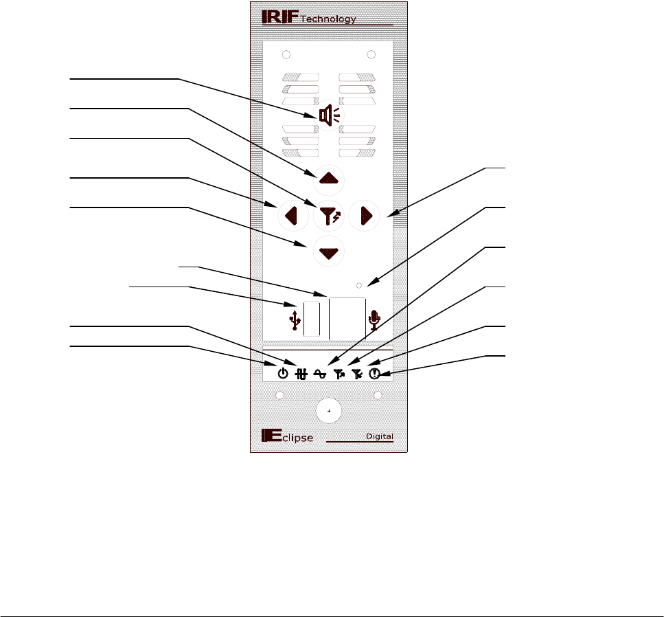
2.1.1 Front Panel Controls and Indicators
The front-panel includes LED indicators, tactile switch buttons, a microphone connector
and an USB (type A) connectors, refer figure.1 for details
Status
Up
Test
Left Right
Down Reset
Analog
Microphone Connector
USB Connector Tx
Digital Rx
Power
Alarm
Figure1: Eclipse2 Transceiver Front panel
2.1.1.1 Buttons:
Status – Press this button to listen the voice report
Test – Press this button to key up the exciter (if front panel test key enabled)
Up – Press this button to increase the speaker volume
2

© RF Technology 2007
Down – Press this button to decrease the speaker volume
Left – Press this button to change channel to next lower programmed number
Right – Press this button to change channel to next higher programmed number
Reset – The reset switch mounted inside base station, used for reset the
transceiver without power cycle, use a small pin (e.g. paper clipper) to
access this switch
2.1.1.2 Indicators:
Power – This LED (on) indicates that DC power supply is applied to the transceiver
Digital – This LED (on) indicates that the transceiver is operating in Digital mode
Analog – This LED (on) indicates that the transceiver is operating in Analog mode,
- if the transceiver is operating in dual mode, both Digital and Analog LED
will be on
Tx – This LED (on) indicates the transceiver’s transmitting path is active
Rx – This LED (on) indicates the transceiver’s receiving path is active
Alarm – This LED (flash) indicates the transceiver is in alarm state, press the
status button to listen the alarm information
2.1.1.3 Connectors:
Microphone – RJ45 connector for front-panel microphone input
USB – USB (type A) connector for connecting host PC via a standard USB cable
to monitor or program the transceiver
2.1.2 Rear Panel Connectors
2.1.2.1 System I/O:
The male D shell, 25-pin connector is the main interface to the transceiver. The pins of
the connection are described in table 1.
Pin No. Description Specification
1, 4 Power supply, positive Input: +13.8VDC
(minimum 10.8V, maximum 16V)
13,25 Power supply, negative Input: Ground
2 System serial bus, Data out Output: +3.3V TTL logic
15 System serial bus, Clock Output: +3.3V TTL logic
3 Exciter PTT input Input: Low active level ≤ +2.5V)
16 Receiver COS output Output: open collector, Imax = 100mA
4 AUX audio input Input: unbalanced 4.7kohm, DC to 3000Hz
5 AUX audio output Output: unbalanced 4.7kohm, DC to
3000Hz
8, 17 Audio signal ground Input: ground
6 Line input + Input: balanced 600ohm,
300 to 3000Hz, -20dbm to +10dbm
19 Line input - Input: balanced 600ohm,
300 to 3000Hz, -20dbm to +10dbm
7 Line output + Output: balanced 600ohm,
300 to 3000Hz, -20dbm to +10dbm

© RF Technology 2007
20 Line output - Output: balanced 600ohm,
300 to 3000Hz, -20dbm to +10dbm
8 GPS 1 pulse/sec input Input: +3.3V to +15V TTL logic
21 Monitor speaker output Output: unbalanced 8 ohm
300 to 3000Hz, 3 Watt maximum
9 System serial bus, Data in Input: +3.3V TTL logic
22 System serial bus, CS0 Output: +3.3V TTL logic
10 System serial bus, CS1 Output: +3.3V TTL logic
23 T/R relay output Output: open collector, Imax = 100mA
11 External squelch input Input: Low active (Vin ≤ +2.5V)
24 Spare GPIO input Input: Low active level ≤ +2.5V)
12 Spare GPIO output Output: open collector, Imax = 100mA
Table1: D25 System I/O Connector signals
2.1.2.2 E/M Line:
This RJ45 connector provides easy connection to the equipment such as microwave
links, the signal of the E/M line connector is described in table2.
Pin No. Description Specification
1 E+ Input: 10V to 48V
2 E- Input: 10V to 48V
3 Line out + Output: balanced 600ohm,
300 to 3000Hz, -20dbm to +10dbm
4 Line out - Output: balanced 600ohm,
300 to 3000Hz, -20dbm to +10dbm
5 Line in + Input: balanced 600ohm,
300 to 3000Hz, -20dbm to +10dbm
6 Line in - Input: balanced 600ohm,
300 to 3000Hz, -20dbm to +10dbm
7 M+ Output: sink current 150mA
8 M- Output: sink current 150mA
Table2: RJ45 E/M Line Connector signals
2.1.2.3 Ethernet:
The RJ45 Ethernet connector is used for networking the base station via IP protocol, a
host PC can use this connector to monitor and control the base station locally or
remotely.
The transceiver supports 10/100Mbs specification (defined by IEEE802.3u) and
MDI/MDI-X auto crossover function which means either straight though or crossover
cable can be used to connect the base station.
There are two LEDs embedded in the RJ45 Ethernet connector, the green LED
indicates that the Ethernet link is active; the yellow LED indicates TX/RX status between
the base station and the network.

© RF Technology 2007
2.1.2.4 RF input:
The receiver RF input connector: 50ohm female, N type.
2.1.2.5 RF output:
The exciter RF output connector: 50ohm female SMA.
2.1.2.6 RS232 and external reference clock (optional)
The female D shell, 9-pin connector is an optional interface to the transceiver. RS232
and external reference clock (EXT_RFE) signals share this connector. The pins of the
connection are described in table 3.
Pin No. Description Specification
1 GND(RS232) Ground
2 TXD (RS232) Output: +/-5V to +/-15V TTL logic
3 RXD(RS232) Input: +/-5V to +/-15V TTL logic
5 GND(RS232) Ground
8 External reference clock Input, sine wave or TTL logic,
Minimum input: 0.5Vp-p
9 GND(EXT_REF) Ground
4, 6, 7 NC No connection on pin 4, 6, 7
Table2: RJ45 E/M Line Connector signals
2.2 PROGRAMMING AND MONITORING
Programming and monitoring is most easily accomplished with RF Technology’s
Service Kit software. This software is based on Java platform and can be run under
various operation systems on the host PC, it provides a number of additional useful
facilities for the base station configurations.
Service Kit software allows configuring of base station (e.g. the channels, output power,
signal path, etc.) without hardware alignment, it also provides a simple means of
calibrating the RF power, RSSI level, line levels. For more details of Service Kit
software, please refer the document: RFT Doc No. 0305917801 (Service Kit Operation
Manual).
Service Kit software and the operation manual can be supplied by your dealer,
distributor or by contacting RF Technology directly.
There are three interfaces which can be used for connecting host PC and base station:

© RF Technology 2007
2.2.1 Connecting with Ethernet
Ethernet is the most powerful interface of the base station, especially for remote
monitoring and controlling via Internet. Each base station has a unique IP address, to
connect, the host PC must be in the same sub net with the base station.
2.2.2 Connecting with USB
The front-panel USB connector can be also used for connecting to host PC, the
operation system need a proper driver to recognize the base station. Make sure the
diver is installed in host PC so that Service Kit can communicate properly with the base
station via the USB interface.
2.2.3 Connecting with RS232 (optional)
The RS232 share the same internal serial port with the USB interface, only one (either
RS232 or USB, if both interface are connected, USB has the priority) of them can be
used at the same time.
Only three wires (TXD, RXD and GND) are used in this RS232 interface. The
transceiver supports up to 115.2kbps data rate, make sure the host PC serial port
setting is 8 data bits, 1 stop bit, none parity and no flow control.
2.3 CIRCUIT DESCRIPTION
The following descriptions should be read as an aid to understanding the block and
schematic diagrams given in the appendix of this manual.
The transceiver consists three major subparts: Processor (Master) board, Interface
(Main) board, and RF modules.
2.3.1 Processor (Master) board
The Processor (Master) board is a six-layer, double side component mounted PCB
assembly. The most important parts of the base station, such as CPU, DSP and digital
IF receiver, are embedded in this master board, two 40-pin connectors on this board
allows user inserting/removing it from the interface (main) board.
The CPU (U1) is a single chip 32-bit RISC processor, it controls all the operating
functions of the base station. The support chips include a 16Mbyte Flash (U9) and
64Mbyte SDRAM (U7, U8). The base station software and configuration databases are
stored in the Flash memory. The system serial bus and GPIO of the RISC processor are
connected to the system interface board via two 40-pin connectors.

© RF Technology 2007
The 10/100Mbps Ethernet Physical Layer single chip transceiver (U10) provides the
interface between RISC processor and the Ethernet. A serial ATA cable is used for
connecting between the Master board and System interface board.
The DSP (U2) is a 32-bit fixed-point digital signal processor, it provides the base band
processing such as: modulation, demodulation, RSSI/SINAD calculation, sub-tone
encoding/decoding and audio processing of the base station. The DSP software is
modularized, the modulator, demodulator, pre-emphasis, de-emphasis, filters and gain
are individual modules, user can connect the disconnect any module by the Service Kit
software for different applications. The DSP also controls the frequencies of the PLL
chips in the RF modules. The digitized audio signal interfaced to the CODEC of the
system interface board is via the DSP serial port.
The digital IF receiver consists an ADC (analog to digital converter, U4) and a DDC
(digital down converter, U3). The pre-filtered analog IF signal from the receiver module
is fed to ADC, converted to the digital IF and passed to the DDC via the parallel bus, the
DDC mixes the incoming digital IF with the internal Numerically Controlled Oscillator
(NCO) frequency signal to produce the 0Hz IF, the DDC also provides decimating and
further filtering for the IF signal. The output from the DDC is in complex I/Q format, sent
to the DSP for demodulating via the serial bus.
The clock of ADC, DDC and DSP is from the system interface board.
2.3.2 Interface (Main) board
The Interface (Main) board provides the interfaces among the Processor (main) board ,
RF modules and external equipment. The function of the Interface board can be
described as following sub sections.
2.3.2.1 Audio signal processing
External audio signals from/to the base station are processed in this section.
The balanced audio input from RJ45 E/M Line connector or D25 system connector is
passed, after line matching transformer (T1) coupling, to a Trans-conductance amplifier
(U11), the gain of the amplifier is controlled by the RISC processor. The output of this
amplification stage is then amplitude limited, attenuated and filtered before send to the
channel 1 of the CODEC (U12). The CODEC encodes the analog audio to digital PCM
signal send to the DSP via the serial bus.
The Microphone input from front panel RJ45 connector is amplified by op-amplifier
(U16), amplitude limited and attenuated then fed to the cannel 2 of the CODEC (U12).
The CODEC encodes the analog audio to digital PCM signal send to the DSP via the
serial bus.
The AUX input signal from D25 system connector is DC coupled, filtered and amplitude
limited by the op-amplifier (U16), then fed into a 16-bit ADC (U17) to convert to the
digital signal. The digitized signal is send to the DSP via the serial bus. This AUX input
is useful for low frequency (down to 0Hz DC) signals, the DC offset of input signal is

© RF Technology 2007
shifted by the bias circuit which is controlled by the RISC processor to give the
maximum dynamic range for the ADC.
The CODEC has two identical channels, the output of channel 1 is used for line output.
PCM signal from the DSP is decoded to analog audio, and amplified, buffered by op-
amplifier U10, coupling through the line matching transformer (T2), and sent to the RJ45
E/M Line connector and the D25 system connector.
The channel 2 output of the CODEC is used for monitor speaker, PCM signal from the
DSP is decoded to analog audio, amplified by a Trans-conductance amplifier (U11), this
amplifier is used as the speaker volume control. The power amplifier (U13) provides
additional power gain to drive the internal and external speaker.
A 16-bit DAC (U14) converts the digital output from the DSP to analog signal, the signal
is filtered and buffered by op-amplifier (U10), then sent to the D25 system connector.
The amplifier is DC coupled, the DC offset can be set by the bias circuit which is
controlled by the RISC processor. This output is useful for low frequency application
such as sub-tone, and NRZ digital signals.
2.3.2.2 I/O and Controls
The RISC processor uses serial buses and GPIO to control the base station.
A 10-bit 11-channel ADC (U7) senses the following signals and passes the data to the
RISC processor via serial bus:
Channel 0: exciter PLL tuning voltage
Channel 1: exciter forward power of the power amplifier
Channel 2: exciter reverse power of the power amplifier
Channel 3: receiver PLL tuning voltage
Channel 4: Interface board temperature
Channel 5: Input power supply voltage
Channel 6: receiver power supply voltage
Other channels are reserved for future usage.
A 10-bit 8-channel DAC (U6) converts data from the RISC processor serial bus to
analog voltage for following functions:
Channel 0: monitor speaker volume control
Channel 1: 600 ohm audio Line input gain control
Channel 2: exciter reverse power of the power amplifier
Channel 3: AUX audio input bias setting
Channel 4: AUX audio output bias setting
Channel 5: receiver IF amplifier gain control (not used in release1 RX module)
Channel 6: exciter RF output power control
Channel 7: exciter VCO bias setting
Channel 8: receiver VCO bias setting
The op-amplifiers (U4, U28) are used for converting DAC output to proper voltage which
is required by the system hardware.

© RF Technology 2007
The Interface board accepts both TTL PTT input and E/M signaling, the TTL PTT is
buffered by Q4,Q5, E/M signal is isolated by Opto-coupler U3 to system I/O level. The
output of the RISC I/O logic is buffered by U1,Q1-Q3 for interfacing the external logic.
The solid-state relay Opto-coupler is used to isolate the system I/O from E/M signal.
A dual retriggerable monostable multivibrator (U5) in the circuit is functioned as a IRQ
generator, it senses the changes of the Input logic and sends a narrow pulse to the
RISC processor for trigging the processing IRQ.
U31 is a USB to RS232 bridge which transfers the USB data between the front panel
connector and the system serial bus. U9 is an transceiver which converts RS232 +/-15
logic from the rear panel to serial bus level. U30 is a bus switch to select one of above
passing through to the RSIC processor.
Header (H4) is used only for emergency system booting purpose, do not assert jumper
into this header.
2.3.2.3 Clock generator
the 12.8MHz TCXO (X1) output is buffered (by U26) and divided by 4 (U29) to provides
PLL reference frequency for exciter and receiver. The frequency doubler double
12.8MHz frequency to 25.6MHz to provide system clock for digital IF receiver.
2.3.2.4 Voltage regulators
There are nine voltage sources generated by the voltage regulator
VTX – +12.5V DC for TX module
VRX – +12.0V DC for RX module
D3V3 – +3.3V DC for Processor (Master) board and 3V TTL logic
A3V – +3.15V DC for analog 3V rail
+12V – +12.0VDC for analog circuits
+5V – +5V DC for TCXO and 5V TTL logic
+1V8 – +1.8V DC for Flash core supply on the Processor (Master) board
-20V – -20.0V DC for TX and RX VCO bias setting
-12V – -12.0VDC for analog circuits
The input power supply voltage is 13.8VDC, LDO (U19, U22) provides 12.5V (Imax =
1.5A) and 12V DC (Imax = 800mA) for TX and RX module. Switch mode DC-DC
converter (U20) generates digital 3.3V DC rail (Imax=2A) for the Processor board and
Interface board, then regulated to 3.15V analog DC rail by LDO (U21) for 3V analog
circuits in the transceiver.
The DC-DC converter (U23) provides –20V negative supply voltage for VCO bias
amplifier (U4). Voltage regulator (U24) generates –12V DC supply analog circuits of the
interface board.
2.3.3 RF modules

© RF Technology 2007
2.3.3.1 TX module
The TX module can be divided into the VCO, PLL, PA and the Data storage section.
The Voltage Controlled Oscillator (VCO)
The Voltage Controlled Oscillator uses a junction FET (Q2) which oscillates at the
required transmitter output frequency. Varactor diodes (D2, D9, D10, and D11) are used
by the PLL and bias control circuits to keep the oscillator on the desired frequency.
Transistor Q1 is used as an active filter to reduce the noise on the oscillator supply
voltage.
The VCO is keyed ON by the RISC processor through Q3, It is keyed ON when any of
the PTT inputs are active or self-calibrations, but OFF at all other times. The VCO
output is amplified by monolythic amplifier U4 before being fed to the PLL chip (U10).
The Phase Locked Loop (PLL)
The frequency reference for the PLL is from the Interface board via a 20pin connector.
A fractional-N PLL synthesiser (U10) is used in the TX module, this fractional-N
synthesiser provides very fine frequency resolution which enables the PLL used as a
FM modulator by modulating the PLL data. The modulation data is provided by DSP via
the serial bus. The phase detector output (charge pump) signal of U10 is smoothed and
filtered by the loop filter to form the tuning voltage for the VCO circuit.
The Power Amplifier (PA)
Amplifiers (U1, U2) increase the VCO output to a sufficient level to drive the power
amplifier (U3). The output power level of the PA is controlled by RISC processor via
bias pin of U3. The directional coupler (D3, D4) detects the forward and reverse power
components, the detected voltages are then amplified by U7 and U8 to provide
proportional dc levels to the RISC processor. The output from U3 is further filtered by
the low pass filter to reduce higher order harmonics. U1, U2 and U3 are not switched on
until the PLL has locked and had time to settle. This prevents any momentary off
channel transmission when the transmitter is keyed.
The Data Storage
Each TX module has an EEPROM for storing the individual module information such as,
TX module serial number, model name, frequency range, calibration data etc. This is
allows user to simply replace the TX module in the transceiver without redo the
alignment and calibration. The data is transferred between EEPROM and RISC
processor via the serial bus.
2.3.3.2 RX module
The RX module can be divided into the Font-end Amplifier, LO, PLL, IF amplifier and
the Data storage section.
The Front-end Amplifier

© RF Technology 2007
A two-pole voltage tuned filter (D6, D7, L18-20, L23 and L24) is used to limit the RF
bandwidth prior to the RF amplifier transistor Q1. The tuning voltage is supplied by the
RISC processor through the bias control. The circuit values are chosen so that the
centre frequency tracks the VCO bias voltage. RF amplifier transistor Q5 is followed by
a second two-pole voltage tuned filter (D4, D5, L7, L11, L14, L21 and L22) which
provides additional image and spurious frequency rejection. The filter output is
connected to the RF input port of the mixer MX1 via a 1.8dB pad.
The Mixer
MX1 is a level 13 double balanced diode ring mixer with excellent Intermodulation
performance. It has a conversion loss of approximately 6 dB. The gain between the
receiver input and the mixer input is approximately 10 dB so that the total gain between
the antenna input and the IF input 3-4dB. The network (C28, C74, L29, L15, L16 and
R20) passes the IF frequency of 45 MHz and terminates the RF and LO components.
The Local Oscillator (LO)
The LO is a Voltage Controlled Oscillator (Q2) which oscillates at the required
transmitter output frequency. Varactor diodes (D2, D9 - D11) are used by the PLL and
bias control circuits to keep the oscillator on the desired frequency. Transistor Q1 is
used as an active filter to reduce the noise on the oscillator supply voltage. Monolithic
amplifiers U1, U2 and transistor Q6 amplify the VCO output to approximately +16dBm
then feed to the mixer via a 3dB pad.
The Phase Locked Loop (PLL)
The frequency reference for the PLL is from the Interface board via a 20pin connector.
A fractional-N PLL synthesiser (U10) is used in the RX module, PLL frequency PLL is
set by DSP via the serial bus. The phase detector output (charge pump) signal of U10 is
smoothed and filtered by the loop filter to form the tuning voltage for the VCO circuit.
The IF Amplifier
The first IF amplifier uses two parallel connected JFET transistors Q3 and Q4 to obtain
8-10 dB gain. The two transistors provide improved dynamic range and input matching
over a single transistor. A 4-pole 45 MHz crystal filter (FIL1, FIL2) is used between the
first and second IF amplifiers. The second IF amplifier (U3, U5) provides additional
35dB gain to drive the digital IF. A two pole crystal filter (FIL3) is used as an anti-alias
filter of the digital IF.
The Data Storage
Each RX module has an EEPROM for storing the individual module information such
as, TX module serial number, model name, frequency range, calibration data etc. This
is allows user to simply replace the RX module in the transceiver without redo the
alignment and calibration. The data is transferred between EEPROM and RISC
processor via the serial bus.

© RF Technology 2007
2.4 FIELD ALIGNMENTS
As the TX and RX module is pre-tuned for the whole operational frequency range and
level adjustment of signal path is done by software (local or remotely), there is no field
alignment required for optimizing the performance.
2.5 SPECIFICATIONS
2.5.1 Description
The transceiver is a digitized, software upgradable radio, The exciter and the receiver
can be configured as base station, repeater or the stand-alone unit. The exciter
normally has maximum 5 Watt output which is used to drive a high power amplifier. It
can also be used alone in lower power applications. The output power can be preset
between 0.3 and 5 watts. All necessary control and 600 ohm line interface circuitry is
included.
2.5.1.1 Channel Capacity
Although most applications are single channel, it can be programmed for up to 256
channels (from CH0 to CH255). Each channel can have it’s own name, TX/RX
frequencies and profiles.
2.5.1.2 Sub Audio Signaling
Full EIA CTCSS capability as well as nonstandard sub tones are built into the modules.
The CTCSS tone can be programmed for each channel in their profiles. This means
each channel can represent a unique TX/RX and tone frequency combination.
2.5.1.3 Channel Programming
The channel information is stored in Flash memory and can be programmed via the
Ethernet, USB or RS232 interface using a Host PC and RF Technology’s Service Kit
software.
2.5.1.4 Channel Selection
Channel can be select by Service Kit or front panel buttons (if enabled).
2.5.2 Physical Configuration
The transceiver is designed to fit in a 19-inch rack mounted frame. The installed height
is 4 RU (178 mm) and the depth 350 mm. The transceiver is 63.5 mm or 2W (two
Eclipse Modules) wide. The weight of the transceiver is approximately 1.6kg

© RF Technology 2007
2.5.3 Electronic Specifications:
2.5.3.1 Overall
Frequency Range: 150MHz to 174MHz
Channel spacing: 12.5kHz / 25kHz
External reference: 5MHz / 10MHz/ 12.8MHz
Monitor speaker output: 3 watts @ 8 ohm
Microphone input: 6 mV RMS @200 ohm
Duty cycle: 100%
Power Supply: +13.8VDC +/-10% (Negative Ground)
Current Drain: 2A Max with 5 Watt TX output power
750mA Max with TX OFF
Operating temperature: -30°C to +60°C
2.5.3.2 Receiver
Frequency Spread: 24MHz
Frequency Stability: +/-1ppm (-30°C to +60°C)
Frequency Step: 1Hz
First IF frequency: 45 MHz
Second IF frequency: 0 Hz
Sensitivity: 12dB SINAD @ -119dBm (0.25uV) RF Input
Selectivity: 80dB for 25kHz Channel spacing
75dB for 12.5kHz Channel spacing
Spurious Rejection: 90dB
Intermodulation: 85dB
Modulation acceptance: 7.5kHz for 25kHz Channel spacing
3.75 kHz for 12.5kHz Channel spacing
Noise squelch: Adjustable from 0 to 26 dB SINAD
Carrier squelch: Adjustable from –120dbm to –60dBm
Audio Response: 300Hz to 3000Hz
+1/-3dB, Flat or 6dB per Octave de-emphasis
Audio Distortion: < 3%
Line output level: -20dbm to +10dbm @600ohm
2.5.3.3 Exciter
Frequency Spread: 24MHz
Frequency Stability: +/-1ppm (-30°C to +60°C)
Frequency Step: 1Hz
Maximum deviation: 5kHz for 25kHz Channel spacing
2.5kHz for 12.5kHz Channel spacing
Output power: 0.3 Watt to 5 Watt programmable
Spurious & harmonics: -36dbm
Hum & Noise: -55dB for 25kHz Channel spacing
-49dB for 12.5 kHz Channel spacing
Audio Response: 300Hz to 3000Hz
+1/-3dB, Flat or 6dB per Octave de-emphasis
Audio Distortion: < 3%
Line input level: -20dbm to +10dbm @600ohm

© RF Technology 2007
2.5.4 Connectors
2.5.4.1 Antenna Connector
Receiver: Type N 50ohm Female Mounted on the module rear panel
Exciter: SMA 50ohm Female Mounted on the module rear panel
2.5.4.2 Power & I/O Connector
25-pin “D” Male Mounted on the rear panel
2.5.4.3 Ethernet Connector
LED Embedded RJ45 Mounted on the rear panel
2.5.4.4 E/M Line Connector
RJ45 Mounted on the rear panel
2.5.4.5 RS232 & External Reference Connector
9-pin “D” Female mounted on the front panel
2.5.4.6 Microphone connector
RJ45 Mounted on the front panel
2.5.4.7 USB
Type A female Mounted on the front panel

© RF Technology 2007
2.6 PART LIST
The part reference of
2.6.1 Processor (Master) board
2.6.2 Interface Main Board
2.6.3 TX module
2.6.4 RX module
PART 3: POWER AMPLIFIER
Operation basics