Realtek Semiconductor RTL8187 802.11b/g RTL8187 miniCard User Manual Realtek RTL8187L DataSheet 1 2
Realtek Semiconductor Corp. 802.11b/g RTL8187 miniCard Realtek RTL8187L DataSheet 1 2
UserManual.wiki
>
Realtek Semiconductor
>
RTL8187 User Manual
Users Manual
Navigation menu
Upload a User Manual
Namespaces
Wiki Guide
HTML
PDF
Info
Views
User Manual
Discussion / Help
Navigation
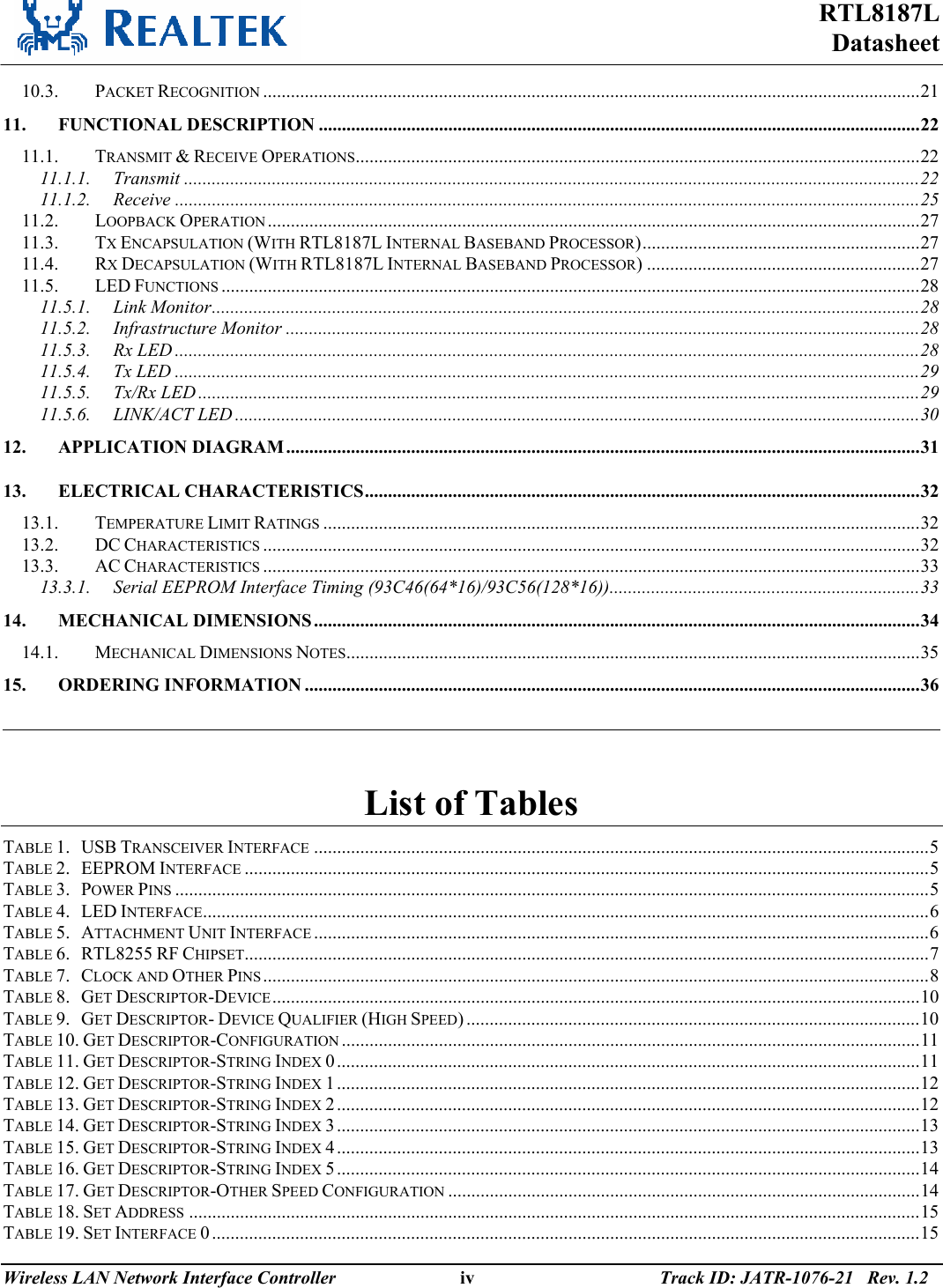
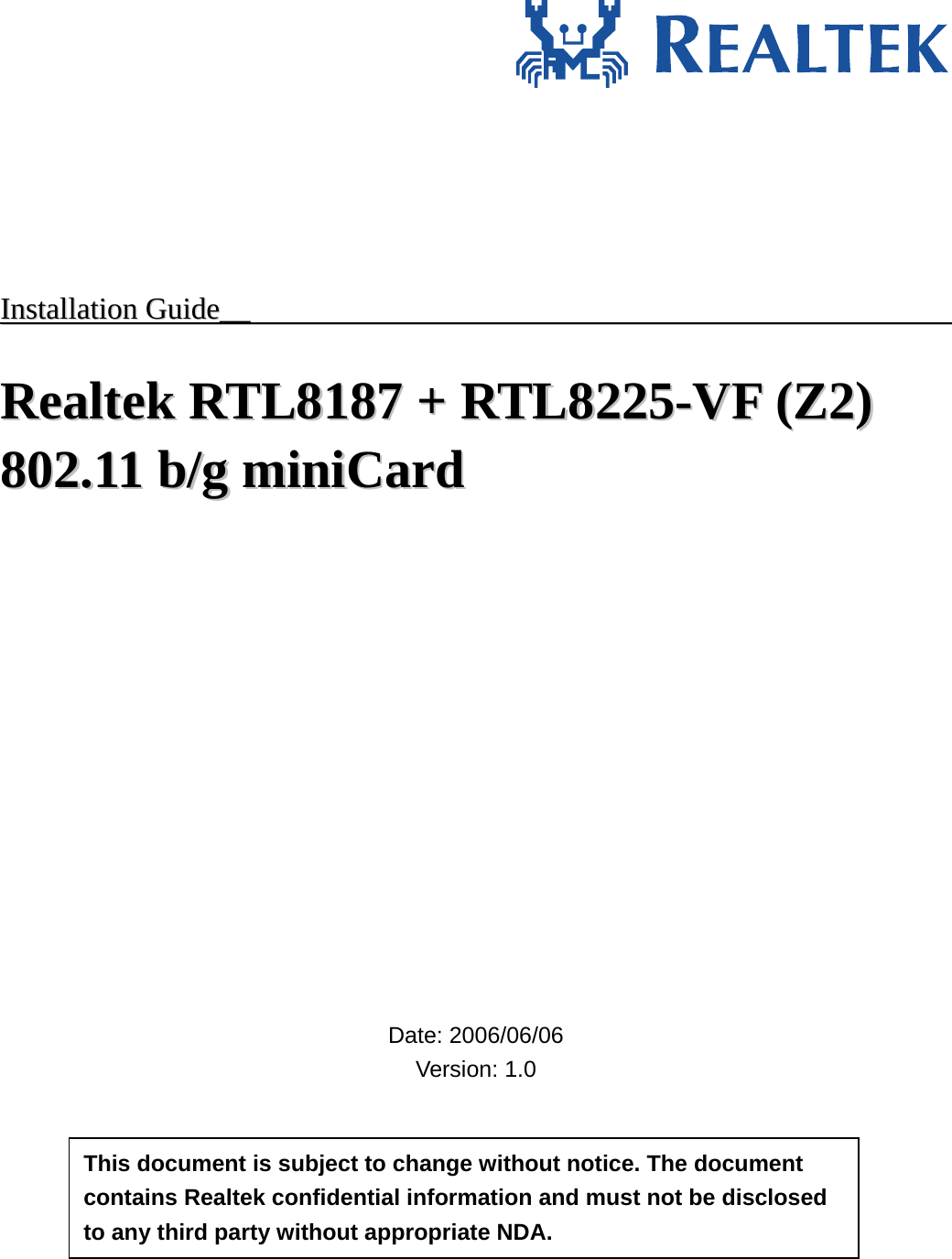
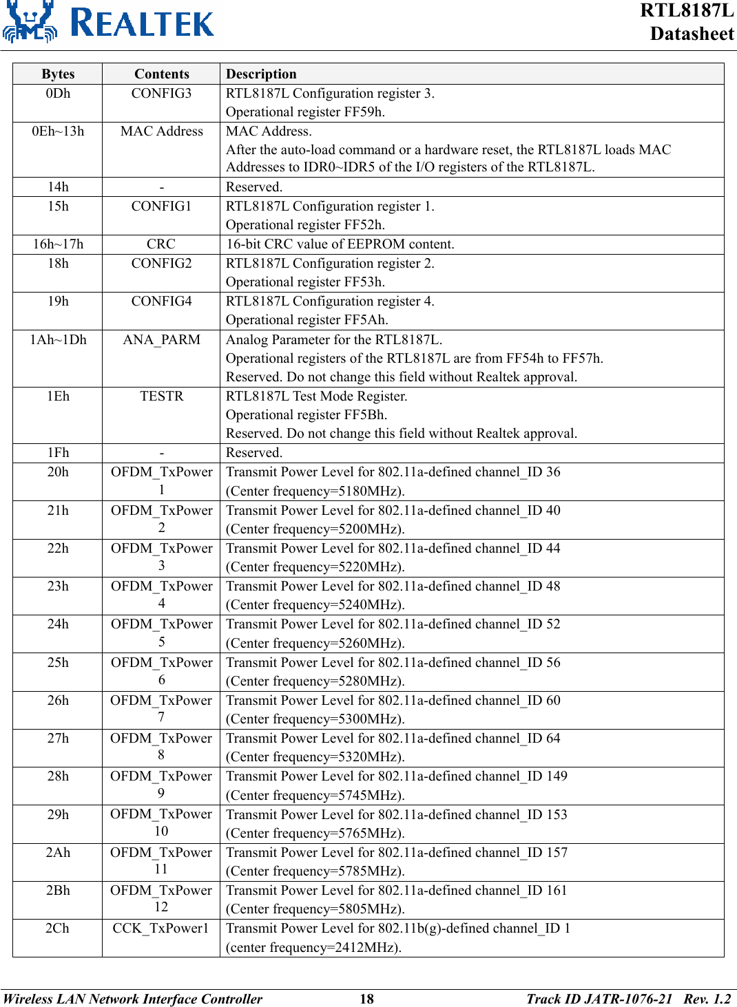
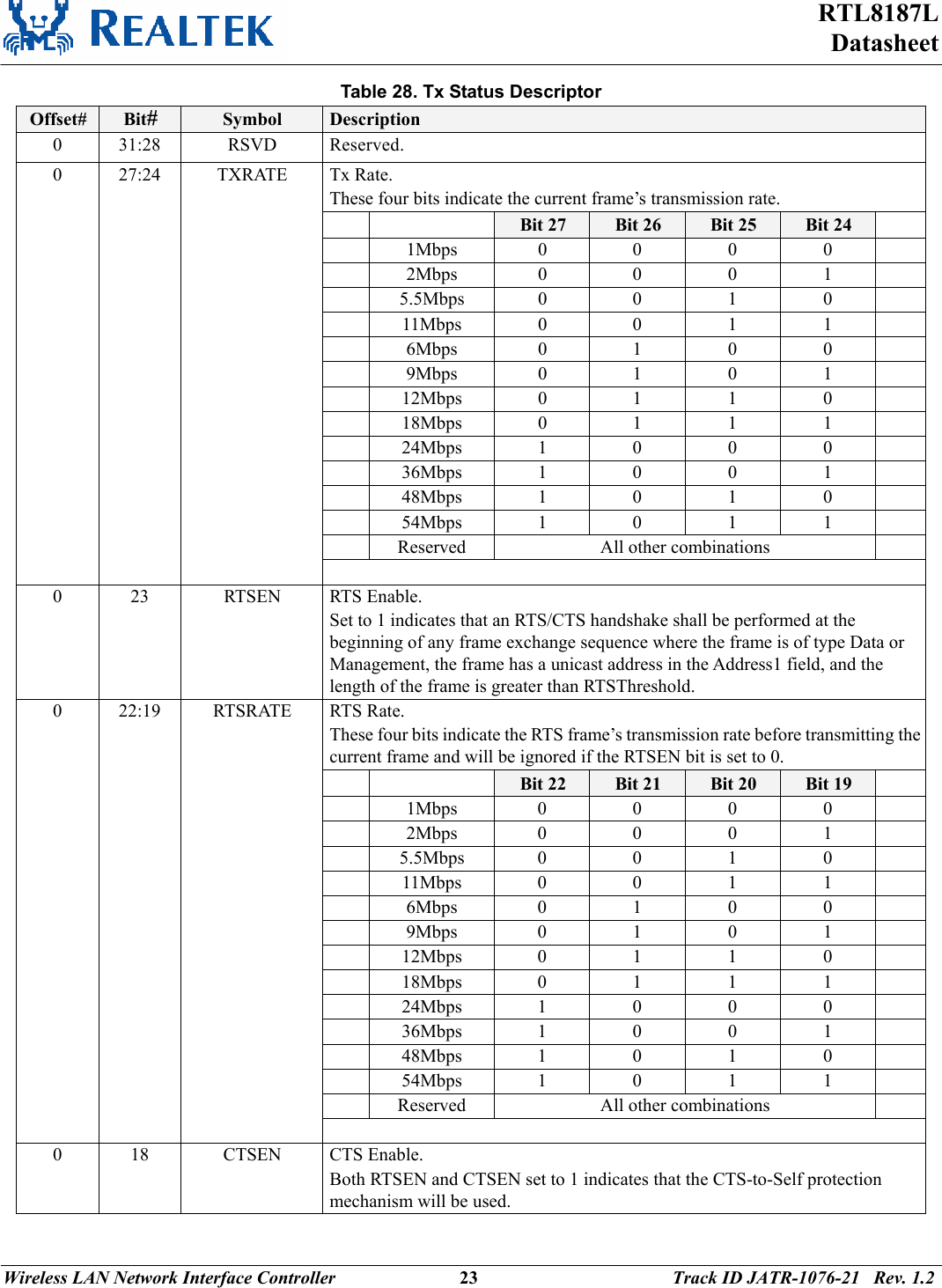
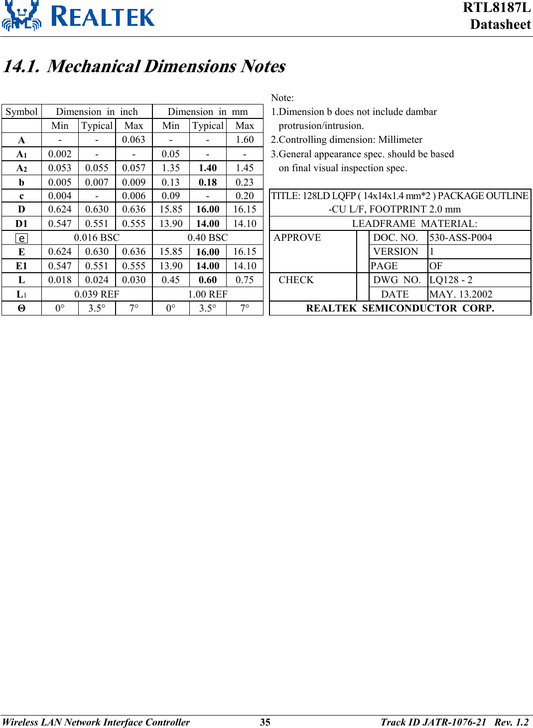
![RTL8187L Datasheet Wireless LAN Network Interface Controller 8 Track ID JATR-1076-21 Rev. 1.2 Symbol Type Pin No Description RFTXEN O 102 Not used in the RTL8255 RF chipset. RFRXEN O 113 Not used in the RTL8255 RF chipset. GPIO[0] O 67 General purpose input/output pin. GPIO[1] O 68 General purpose input/output pin. GPIO[2] O 69 General purpose input/output pin. GPIO[3] O 70 General purpose input/output pin. GPIO[4] O 100 General purpose input/output pin. GPIO[5] O 94 General purpose input/output pin. VREFO X 118 Not used in the RTL8255 RF chipset. VRP X 119 Not used in the RTL8255 RF chipset. VRN X 120 Not used in the RTL8255 RF chipset. RXIP RXIN I I 121 122 Receive (Rx) In-phase Analog Data. RXQP RXQN I I 124 125 Receive (Rx) Quadrature-phase Analog Data. RXAGC O 4 Not used in the RTL8255 RF chipset. TXAGC O 5 Not used in the RTL8255 RF chipset. RSSI I 6 Analog Input to the Receive Power A/D Converter for Receive AGC Control. TSSI0 I 7 Input to the Transmit Power A/D Converter for 2.4GHz Transmit AGC Control. TSSI1 I 8 Input to the Transmit Power A/D Converter for 5GHz Transmit AGC Control. TXQP TXQN O O 11 12 Transmit (TX) Quadrature-phase Analog Data. TXIP TXIN O O 14 13 Transmit (TX) In-phase Analog Data. TXQTP TXQTN O O 15 16 Not used in the RTL8255 RF chipset. TXITP TXITN O O 17 18 Not used in the RTL8255 RF chipset. 6.6. Clock and Other Pins Table 7. Clock and Other Pins Symbol Type Pin No Description R15K I/O 1 This pin must be pulled low by a 15K Ω resistor. XI I 20 40MHz OSC Input.](https://usermanual.wiki/Realtek-Semiconductor/RTL8187/User-Guide-690991-Page-14.png)
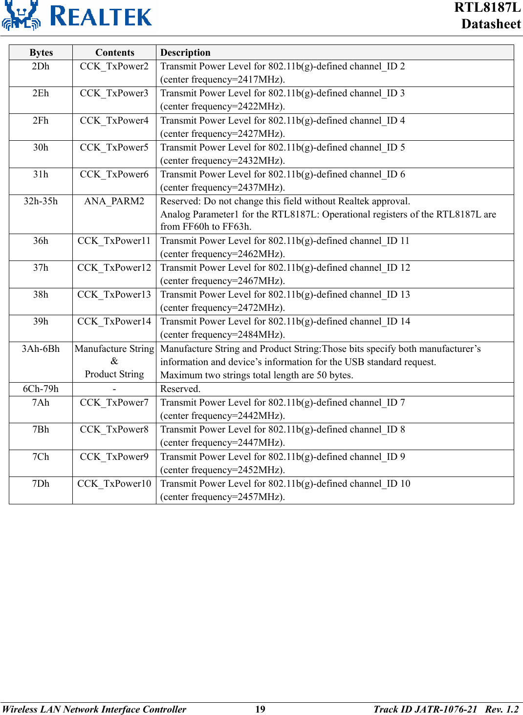
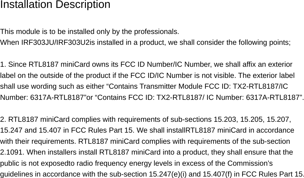
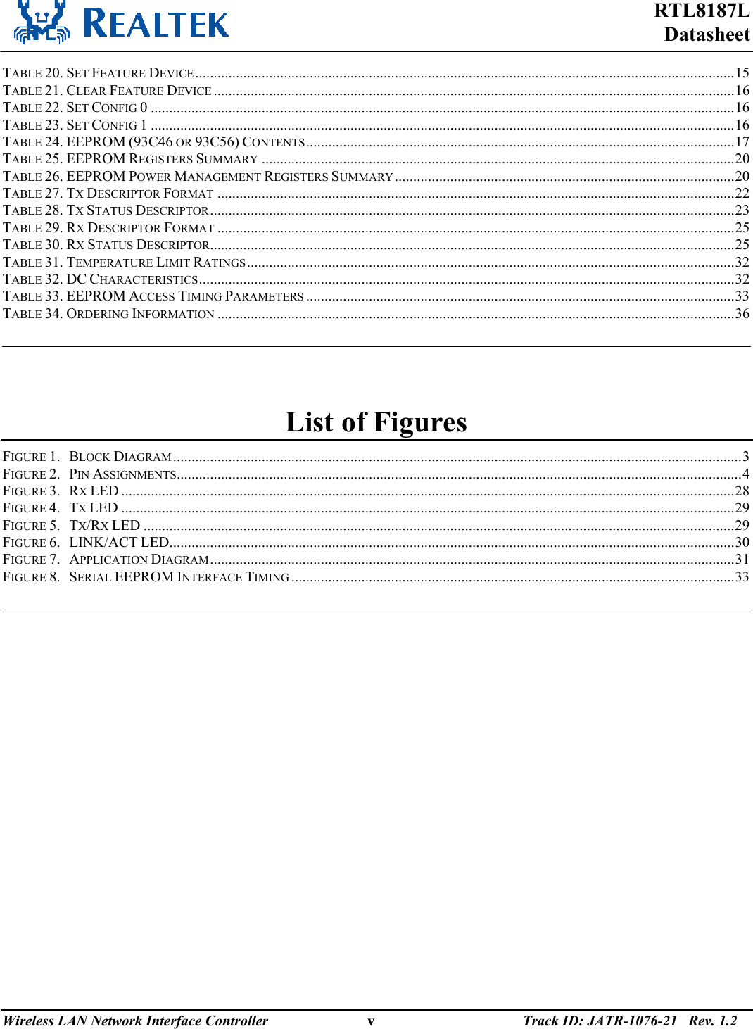
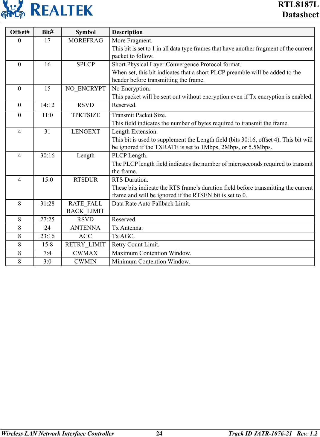
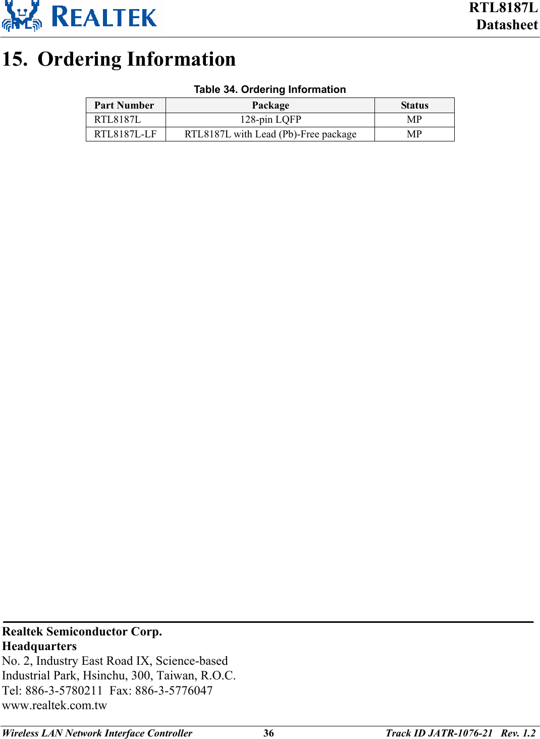
![RTL8187L Datasheet Wireless LAN Network Interface Controller 20 Track ID JATR-1076-21 Rev. 1.2 9.1. EEPROM Registers Summary Table 25. EEPROM Registers Summary Address Name Type Bit7 Bit6 Bit5 Bit4 Bit3 Bit2 Bit1 Bit0 FF00h- FF05h IDR0 – IDR5 R/W* R LEDS1 LEDS0 - LWACT - - - - FF52h CONFIG1 W* LEDS1 LEDS0 - LWACT - - - - R LCK - - - - PAPE _sign PAPE _time FF53h CONFIG2 W* - - - - - PAPE _sign PAPE _time FF54h- FF57h ANA_PARM R/W** 32-bit Read Write R - PARM_En Magic - - - - - FF59h CONFIG3 W* - PARM_En Magic - - - - - R - - - LWPME - LWPTN - FF5Ah CONFIG4 W* - - - LWPME - LWPTN - FF5Bh TESTR 8-bit Read Write FF60h- FF63h ANA_PARM2 R/W 32-bit Read Write FFD8h CONFIG5 R/W** - - - - - - LANWake - Note 1: Registers marked 'W*' can be written only if bits EEM1=EEM0=1. Note 2: Registers marked 'W**' can be written only if bits EEM1:0=[1:1] and CONFIG3<PARM_EN>= 0. 9.2. EEPROM Power Management Registers Summary Table 26. EEPROM Power Management Registers Summary Configuration Space Offset Name Type Bit7 Bit6 Bit5 Bit4 Bit3 Bit2 Bit1 Bit0 52h R Aux_I_b1 Aux_I_b0 DSI Reserved PMECLK Version 53h PMC R PME_D3cold PME_D3hot PME_D2 PME_D1 PME_D0 D2 D1 Aux_I_b2](https://usermanual.wiki/Realtek-Semiconductor/RTL8187/User-Guide-690991-Page-26.png)
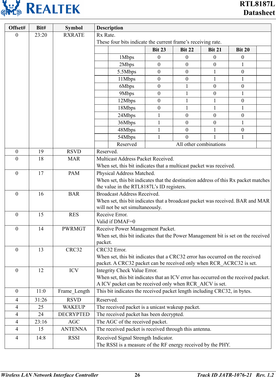
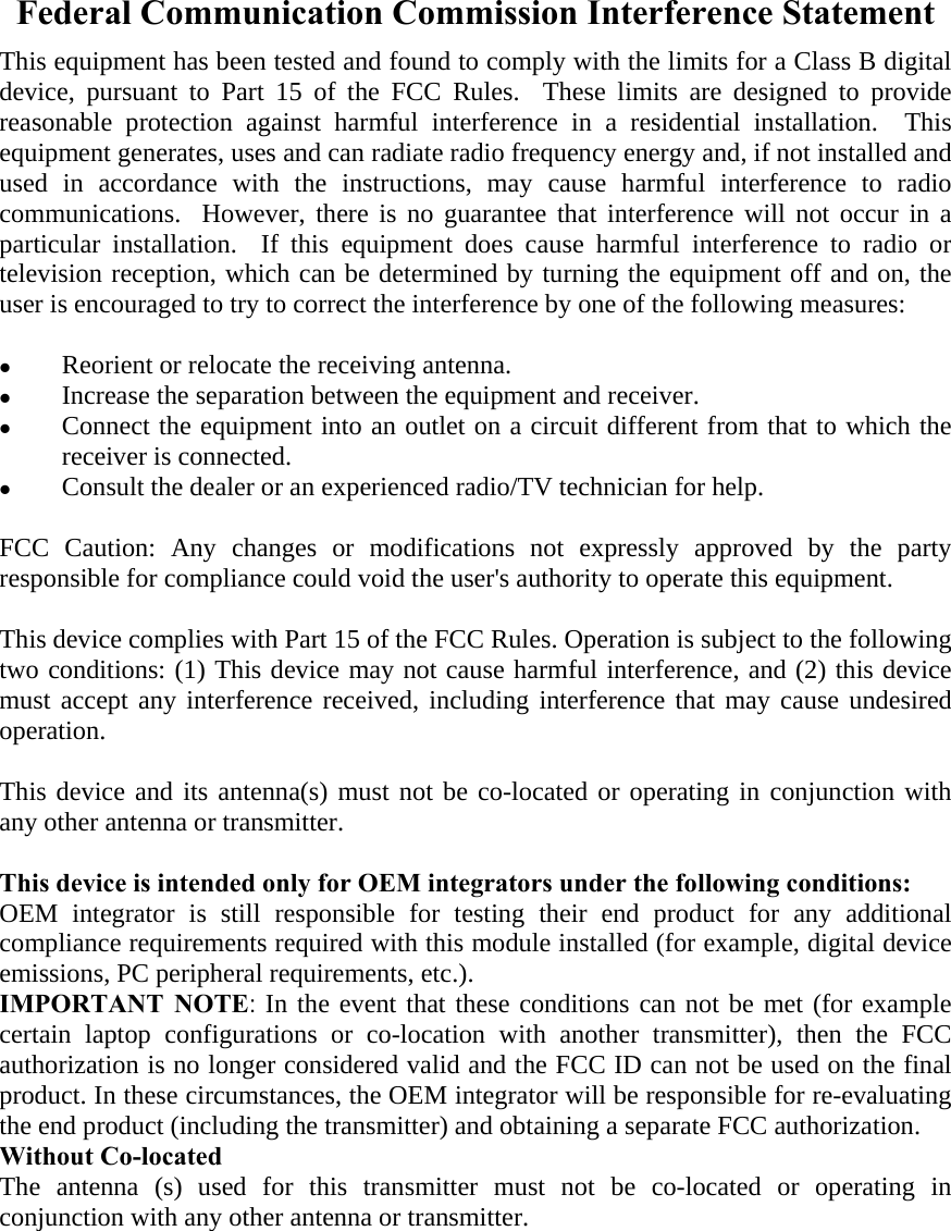
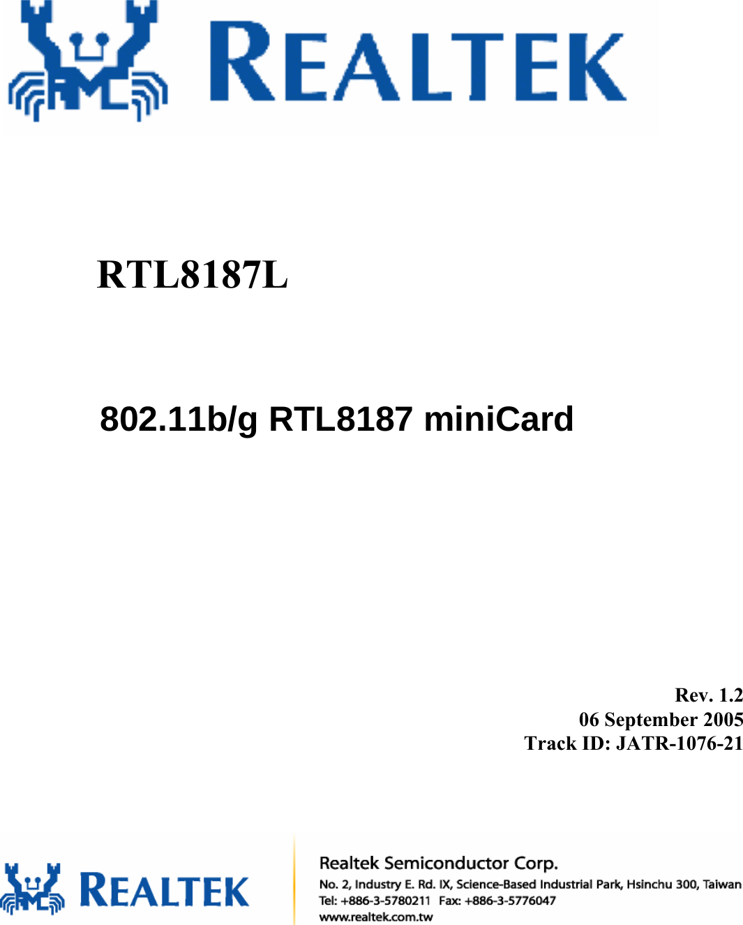
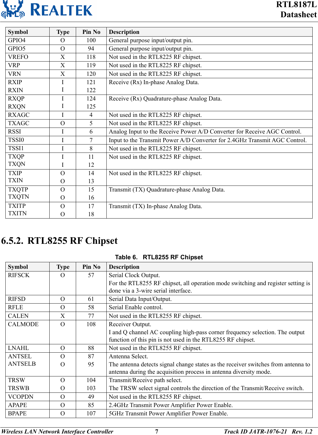
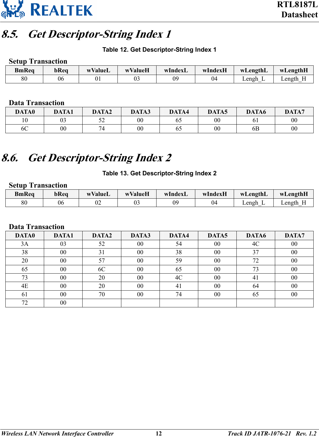
![This device has been designed to operate with an antenna having a maximum gain of [3.00] dBi. Antenna having a higher gain is strictly prohibited per regulations of Industry Canada. The required antenna impedance is 50 ohms." List of antennas below: Ant. Type PIFA PK Gain(dBi) 3 Ant. Type PIFA PK Gain(dBi) 2.32 1. Connector IPEX Model No. DQ661500301 2. Connector IPEX Model No. MA6001 Ant. Type PIFA PK Gain(dBi) 2.39 Ant. Type PIFA PK Gain(dBi) 2.11 3. Connector IPEX Model No. AR830WIPI02A 4. Connector IPEX Model No. AR320WIPI02BAnt. Type PIFA PK Gain(dBi) 0.78 Ant. Type PIFA PK Gain(dBi) 1.1 5. Connector IPEX Model No. WDAN-QMA6002-DF 6. Connector IPEX Model No. DQ661500115 Ant. Type PIFA PK Gain(dBi) 0.3 Ant. Type PIFA PK Gain(dBi) 2.57 7. Connector IPEX Model No. AAFJ5050002LF0 8. Connector IPEX Model No. AR620WIPI02CAnt. Type PIFA PK Gain(dBi) 1.97 Ant. Type PIFA PK Gain(dBi) 1 9. Connector IPEX Model No. ARMK8WIPI02A 10. Connector IPEX Model No. ARMK8WIPI02AAnt. Type PIFA PK Gain(dBi) 2.37 Ant. Type PIFA PK Gain(dBi) 2.11 11. Connector IPEX Model No. AAFA5050004LQ0 12. Connector IPEX Model No. AR320WIPI01BAnt. Type PIFA PK Gain(dBi) 2.57 Ant. Type PIFA PK Gain(dBi) 2.21 13. Connector IPEX Model No. B078502800000314. Connector IPEX Model No. AR330WIPI01DAnt. Type PIFA PK Gain(dBi) 2.55 Ant. Type PIFA PK Gain(dBi) 2.48 15. Connector IPEX Model No. AR621WIPI02D 16. Connector IPEX Model No. ARW62WIPI01GAnt. Type PIFA PK Gain(dBi) 2.49 Ant. Type PIFA PK Gain(dBi) 0.46 17. Connector IPEX Model No. ARK8MWIPI01B 18. Connector IPEX Model No. AAFQ5050001LK0 Ant. Type PIFA PK Gain(dBi) 2.86 Ant. Type PIFA PK Gain(dBi) 2.45 19. Connector IPEX Model No. AAFQ5050002LK0 20. Connector IPEX Model No. B0125028000004 Ant. Type PIFA PK Gain(dBi) 0.74 Ant. Type PIFA PK Gain(dBi) 0.03 21. Connector IPEX Model No. MA6002 22. Connector IPEX Model No. W340UA1 To reduce potential radio interference to other users, the antenna type and its gain should be so chosen that the equivalent isotropically radiated power (e.i.r.p.) is not more than that permitted for successful communication.](https://usermanual.wiki/Realtek-Semiconductor/RTL8187/User-Guide-690991-Page-45.png)