Realtek Semiconductor RTL8187 802.11b/g RTL8187 miniCard User Manual Realtek RTL8187L DataSheet 1 2
Realtek Semiconductor Corp. 802.11b/g RTL8187 miniCard Realtek RTL8187L DataSheet 1 2
Users Manual

802.11b/g RTL8187 miniCard
Rev. 1.2
06 September 2005
Track ID: JATR-1076-21
RTL8187L

RTL8187L
Datasheet
Wireless LAN Network Interface Controller ii Track ID: JATR-1076-21 Rev. 1.2
COPYRIGHT
©2005 Realtek Semiconductor Corp. All rights reserved. No part of this document may be reproduced,
transmitted, transcribed, stored in a retrieval system, or translated into any language in any form or by any
means without the written permission of Realtek Semiconductor Corp.
DISCLAIMER
Realtek provides this document “as is”, without warranty of any kind, neither expressed nor implied,
including, but not limited to, the particular purpose. Realtek may make improvements and/or changes in
this document or in the product described in this document at any time. This document could include
technical inaccuracies or typographical errors.
TRADEMARKS
Realtek is a trademark of Realtek Semiconductor Corporation. Other names mentioned in this document are
trademarks/registered trademarks of their respective owners.
USING THIS DOCUMENT
This document is intended for the software engineer’s reference and provides detailed programming
information.
Though every effort has been made to ensure that this document is current and accurate, more information
may have become available subsequent to the production of this guide. In that event, please contact your
Realtek representative for additional information that may help in the development process.
REVISION HISTORY
Revision Release Date Summary
1.0 2004/10/22 First release.
1.1 2005/04/25 Revised data transaction content.
Added offset 8 information (Table 27, page 23, and Table 28, page 23).
1.2 2005/09/06 Added RoHS declaration (see last 2 pages).
Added lead (Pb)-free and package identification information on page 4.
Corrected section 14 Mechanical Dimensions, page 34.

RTL8187L
Datasheet
Wireless LAN Network Interface Controller iii Track ID: JATR-1076-21 Rev. 1.2
Table of Contents
1. GENERAL DESCRIPTION ...............................................................................................................................................1
2. FEATURES ..........................................................................................................................................................................2
3. SYSTEM APPLICATIONS ................................................................................................................................................3
4. BLOCK DIAGRAM ............................................................................................................................................................3
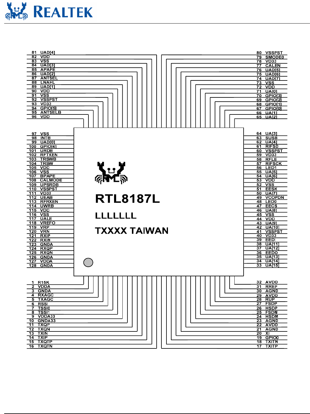
5. PIN ASSIGNMENTS...........................................................................................................................................................4
5.1. LEAD (PB)-FREE PACKAGE IDENTIFICATION ...................................................................................................................4
6. PIN DESCRIPTIONS ..........................................................................................................................................................5
6.1. USB TRANSCEIVER INTERFACE ......................................................................................................................................5
6.2. EEPROM INTERFACE .....................................................................................................................................................5
6.3. POWER PINS ....................................................................................................................................................................5
6.4. LED INTERFACE..............................................................................................................................................................6
6.5. ATTACHMENT UNIT INTERFACE ......................................................................................................................................6
6.5.1. RTL8225 RF Chipset..............................................................................................................................................6
6.5.2. RTL8255 RF Chipset..............................................................................................................................................7
6.6. CLOCK AND OTHER PINS.................................................................................................................................................8
7. CPU ACCESS TO ENDPOINT DATA..............................................................................................................................9
7.1. CONTROL TRANSFER.......................................................................................................................................................9
7.2. BULK TRANSFER .............................................................................................................................................................9
8. USB REQUEST..................................................................................................................................................................10
8.1. GET DESCRIPTOR-DEVICE.............................................................................................................................................10
8.2. GET DESCRIPTOR-DEVICE QUALIFIER (HIGH SPEED)....................................................................................................10
8.3. GET DESCRIPTOR-CONFIGURATION ..............................................................................................................................11
8.4. GET DESCRIPTOR-STRING INDEX 0 ...............................................................................................................................11
8.5. GET DESCRIPTOR-STRING INDEX 1 ...............................................................................................................................12
8.6. GET DESCRIPTOR-STRING INDEX 2 ...............................................................................................................................12
8.7. GET DESCRIPTOR-STRING INDEX 3 ...............................................................................................................................13
8.8. GET DESCRIPTOR-STRING INDEX 4 ...............................................................................................................................13
8.9. GET DESCRIPTOR-STRING INDEX 5 ...............................................................................................................................14
8.10. GET DESCRIPTOR-OTHER SPEED CONFIGURATION....................................................................................................14
8.11. SET ADDRESS ............................................................................................................................................................15
8.12. SET INTERFACE 0 ......................................................................................................................................................15
8.13. SET FEATURE DEVICE ...............................................................................................................................................15
8.14. CLEAR FEATURE DEVICE ..........................................................................................................................................16
8.15. SET CONFIG 0............................................................................................................................................................16
8.16. SET CONFIG 1............................................................................................................................................................16
9. EEPROM (93C46 OR 93C56) CONTENTS....................................................................................................................17
9.1. EEPROM REGISTERS SUMMARY..................................................................................................................................20
9.2. EEPROM POWER MANAGEMENT REGISTERS SUMMARY .............................................................................................20
10. USB PACKET BUFFERING ........................................................................................................................................21
10.1. TRANSMIT BUFFER MANAGER ..................................................................................................................................21
10.2. RECEIVE BUFFER MANAGER .....................................................................................................................................21

RTL8187L
Datasheet
Wireless LAN Network Interface Controller iv Track ID: JATR-1076-21 Rev. 1.2
10.3. PACKET RECOGNITION ..............................................................................................................................................21
11. FUNCTIONAL DESCRIPTION ..................................................................................................................................22
11.1. TRANSMIT & RECEIVE OPERATIONS..........................................................................................................................22
11.1.1. Transmit ...............................................................................................................................................................22
11.1.2. Receive .................................................................................................................................................................25
11.2. LOOPBACK OPERATION .............................................................................................................................................27
11.3. TX ENCAPSULATION (WITH RTL8187L INTERNAL BASEBAND PROCESSOR)............................................................27
11.4. RX DECAPSULATION (WITH RTL8187L INTERNAL BASEBAND PROCESSOR) ...........................................................27
11.5. LED FUNCTIONS .......................................................................................................................................................28
11.5.1. Link Monitor.........................................................................................................................................................28
11.5.2. Infrastructure Monitor .........................................................................................................................................28
11.5.3. Rx LED .................................................................................................................................................................28
11.5.4. Tx LED .................................................................................................................................................................29
11.5.5. Tx/Rx LED ............................................................................................................................................................29
11.5.6. LINK/ACT LED ....................................................................................................................................................30
12. APPLICATION DIAGRAM.........................................................................................................................................31
13. ELECTRICAL CHARACTERISTICS........................................................................................................................32
13.1. TEMPERATURE LIMIT RATINGS .................................................................................................................................32
13.2. DC CHARACTERISTICS ..............................................................................................................................................32
13.3. AC CHARACTERISTICS ..............................................................................................................................................33
13.3.1. Serial EEPROM Interface Timing (93C46(64*16)/93C56(128*16))...................................................................33
14. MECHANICAL DIMENSIONS...................................................................................................................................34
14.1. MECHANICAL DIMENSIONS NOTES............................................................................................................................35
15. ORDERING INFORMATION .....................................................................................................................................36
List of Tables
TABLE 1. USB TRANSCEIVER INTERFACE .....................................................................................................................................5
TABLE 2. EEPROM INTERFACE ....................................................................................................................................................5
TABLE 3. POWER PINS ...................................................................................................................................................................5
TABLE 4. LED INTERFACE.............................................................................................................................................................6
TABLE 5. ATTACHMENT UNIT INTERFACE .....................................................................................................................................6
TABLE 6. RTL8255 RF CHIPSET....................................................................................................................................................7
TABLE 7. CLOCK AND OTHER PINS ................................................................................................................................................8
TABLE 8. GET DESCRIPTOR-DEVICE............................................................................................................................................10
TABLE 9. GET DESCRIPTOR- DEVICE QUALIFIER (HIGH SPEED) ..................................................................................................10
TABLE 10. GET DESCRIPTOR-CONFIGURATION .............................................................................................................................11
TABLE 11. GET DESCRIPTOR-STRING INDEX 0 ..............................................................................................................................11
TABLE 12. GET DESCRIPTOR-STRING INDEX 1 ..............................................................................................................................12
TABLE 13. GET DESCRIPTOR-STRING INDEX 2 ..............................................................................................................................12
TABLE 14. GET DESCRIPTOR-STRING INDEX 3 ..............................................................................................................................13
TABLE 15. GET DESCRIPTOR-STRING INDEX 4 ..............................................................................................................................13
TABLE 16. GET DESCRIPTOR-STRING INDEX 5 ..............................................................................................................................14
TABLE 17. GET DESCRIPTOR-OTHER SPEED CONFIGURATION ......................................................................................................14
TABLE 18. SET ADDRESS ..............................................................................................................................................................15
TABLE 19. SET INTERFACE 0 .........................................................................................................................................................15

RTL8187L
Datasheet
Wireless LAN Network Interface Controller v Track ID: JATR-1076-21 Rev. 1.2
TABLE 20. SET FEATURE DEVICE..................................................................................................................................................15
TABLE 21. CLEAR FEATURE DEVICE .............................................................................................................................................16
TABLE 22. SET CONFIG 0 ..............................................................................................................................................................16
TABLE 23. SET CONFIG 1 ..............................................................................................................................................................16
TABLE 24. EEPROM (93C46 OR 93C56) CONTENTS....................................................................................................................17
TABLE 25. EEPROM REGISTERS SUMMARY ................................................................................................................................20
TABLE 26. EEPROM POWER MANAGEMENT REGISTERS SUMMARY............................................................................................20
TABLE 27. TX DESCRIPTOR FORMAT ............................................................................................................................................22
TABLE 28. TX STATUS DESCRIPTOR..............................................................................................................................................23
TABLE 29. RX DESCRIPTOR FORMAT ............................................................................................................................................25
TABLE 30. RX STATUS DESCRIPTOR..............................................................................................................................................25
TABLE 31. TEMPERATURE LIMIT RATINGS....................................................................................................................................32
TABLE 32. DC CHARACTERISTICS.................................................................................................................................................32
TABLE 33. EEPROM ACCESS TIMING PARAMETERS ....................................................................................................................33
TABLE 34. ORDERING INFORMATION ............................................................................................................................................36
List of Figures
FIGURE 1. BLOCK DIAGRAM..........................................................................................................................................................3
FIGURE 2. PIN ASSIGNMENTS.........................................................................................................................................................4
FIGURE 3. RX LED ......................................................................................................................................................................28
FIGURE 4. TX LED ......................................................................................................................................................................29
FIGURE 5. TX/RX LED ................................................................................................................................................................29
FIGURE 6. LINK/ACT LED.........................................................................................................................................................30
FIGURE 7. APPLICATION DIAGRAM..............................................................................................................................................31
FIGURE 8. SERIAL EEPROM INTERFACE TIMING ........................................................................................................................33

RTL8187L
Datasheet
Wireless LAN Network Interface Controller 1 Track ID JATR-1076-21 Rev. 1.2
1. General Description
The Realtek RTL8187L is a low-profile highly integrated cost-effective Wireless LAN USB 2.0 network
interface controller that integrates a USB 2.0 PHY, SIE (Serial Interface Engine), 8051 MCU, a Wireless
LAN MAC, and a Direct Sequence Spread Spectrum/OFDM baseband processor onto one chip. It provides
USB high speed (480Mbps), and full speed (12Mbps), and supports 4 endpoints for transfer pipes. To
reduce protocol overhead, the RTL8187L supports Short InterFrame Space (SIFS) burst mode to send
packets back-to-back. A protection mechanism prevents collisions among 802.11b nodes. The RTL8187L
fully complies with IEEE 802.11a/b/g specifications.
Direct Sequence Spread Spectrum (DSSS), Complementary Code Keying (CCK), and Orthogonal
Frequency Division Multiplexing (OFDM) baseband processing are implemented to support all IEEE
802.11a, 802.11b, and 802.11g data rates. Differential phase shift keying modulation schemes, DBPSK and
DQPSK with data scrambling capability, are available, along with complementary code keying to provide
data rates of 1, 2, 5.5, and 11Mbps, with long or short preamble. A high-speed Fast Fourier Transform
(FFT)/Inverse Fast Fourier Transform (IFFT), combined with BPSK, QPSK, 16QAM and 64QAM
modulation of the individual sub-carriers, provides data rates of 6, 9, 12, 18, 24, 36, 48 and 54Mbps, with
rate-compatible punctured convolutional coding with a coding rate of 1/2, 2/3, and 3/4.
An enhanced signal detector, an adaptive frequency domain equalizer, and a soft-decision Viterbi decoder
are built-in to alleviate severe multipath effects. Efficient IQ-imbalance calibration, DC offset, phase noise,
frequency offset, and timing offset compensation reduce radio frequency front-end impairments. Selectable
digital transmit and receiver FIR filters are provided to meet the requirements of transmit spectrum masks,
and to reject adjacent channel interference, respectively. Both in the transmitter and receiver,
programmable scaling in the digital domain trades the quantization noise against the increased probability
of clipping. Robust signal detection, symbol boundary detection, and channel estimation perform well at
the minimum sensitivity.
The RTL8187L supports fast receiver Automatic Gain Control (AGC) and antenna diversity functions, and
an adaptive transmit power control function to obtain better performance in the analog portions of the
transceiver. It also has on-chip digital-to-analog converters and analog-to-digital converters for analog I
and Q inputs and outputs, transmit TSSI and receiver RSSI inputs, and transmit and receiver AGC outputs.
The RTL8187L is highly integrated and requires no ‘glue’ logic or external memory. It keeps network
maintenance costs low and eliminates usage barriers.

RTL8187L
Datasheet
Wireless LAN Network Interface Controller 2 Track ID JATR-1076-21 Rev. 1.2
2. Features
128-Pin LQFP and 128-pin LQFP Lead
(Pb)-Free package
State machine implementation without
external memory (RAM, flash) requirement
Complies with IEEE 802.11a/b/g standards
Supports descriptor-based buffer
management
Integrated Wireless LAN MAC and Direct
Sequence Spread Spectrum/OFDM
Baseband Processor in one chip
Enhanced signal detector, adaptive frequency
domain equalizer, and soft-decision Viterbi
decoder to alleviate severe multipath effects
Processing Gain compliant with FCC
On-Chip A/D and D/A converters for I/Q
Data, AGC, and Adaptive Power Control
Supports both transmit and receive Antenna
Diversity
Data rates of 1, 2, 5.5, 6, 9, 11, 12, 18, 24, 36,
48, and 54Mbps
Supports 40MHz OSC as the internal clock
source. The frequency deviation of the OSC
must be within 25 PPM on IEEE 802.11g and
20 PPM on IEEE 802.11a
IEEE 802.11g protection mechanisms for
both RTS/CTS and CTS-to-self
Burst-mode support for dramatically
enhanced throughput
DSSS with DBPSK and DQPSK, CCK
modulations and demodulations supported
with long and short preamble
OFDM with BPSK, QPSK, 16QAM and
64QAM modulations and demodulations
supported with rate compatible punctured
convolutional coding with coding rate of 1/2,
2/3, and 3/4
Efficient IQ-imbalance calibration, DC
offset, phase noise, frequency offset and
timing offset compensation reduce analog
front-end impairments
Selectable digital transmit and receiver FIR
filters provided to meet transmit spectrum
mask requirements and to reject adjacent
channel interference
Programmable scaling both in transmitter
and receiver to trade quantization noise
against the increased probability of clipping
Fast receiver Automatic Gain Control (AGC)
& antenna diversity functions
Hardware-based IEEE 802.11i
encryption/decryption engine, including
64-bit/128-bit WEP, TKIP, and AES
Supports Wi-Fi alliance WPA and WPA2
security
Contains two large independent transmit and
receive FIFO buffers
Advanced power saving mode when the
LAN and wakeup function are not used
Uses 93C46 (64*16-bit EEPROM) or 93C56
(128*16-bit EEPROM) to store resource
configuration and ID parameter data
LED pins for various network activity
indications
Two GPIO pins supported

RTL8187L
Datasheet
Wireless LAN Network Interface Controller 3 Track ID JATR-1076-21 Rev. 1.2
Supports digital loopback capability on both
ports
Scatter and gather operation
Complies with USB Specification 2.0
Supports Full-speed (12Mbps) and
High-speed (480Mbps)
Embedded standard 8051 CPU with
enhanced features:
Four cycles per instruction
Variable clock speed cuts power
consumption
Supports 4 endpoints:
64-Byte buffer for control endpoint
512-Byte buffer for bulk IN endpoint
Two 512-Byte buffers for bulk OUT
endpoint
3.3V and 1.8V power supplies required
5V tolerant I/Os
0.18µm CMOS process
3. System Applications
USB Dongle WLAN adapter
Embedded WLAN solution in notebook, desktop, mobile phone, and motherboard
RTL8187L
Datasheet
Wireless LAN Network Interface Controller 3 Track ID JATR-1076-21 Rev. 1.2
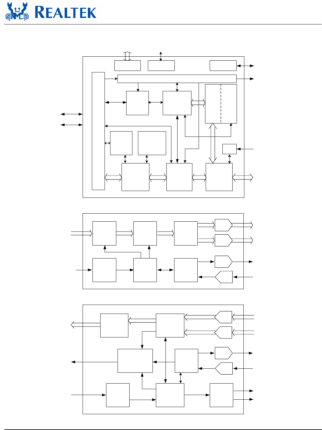
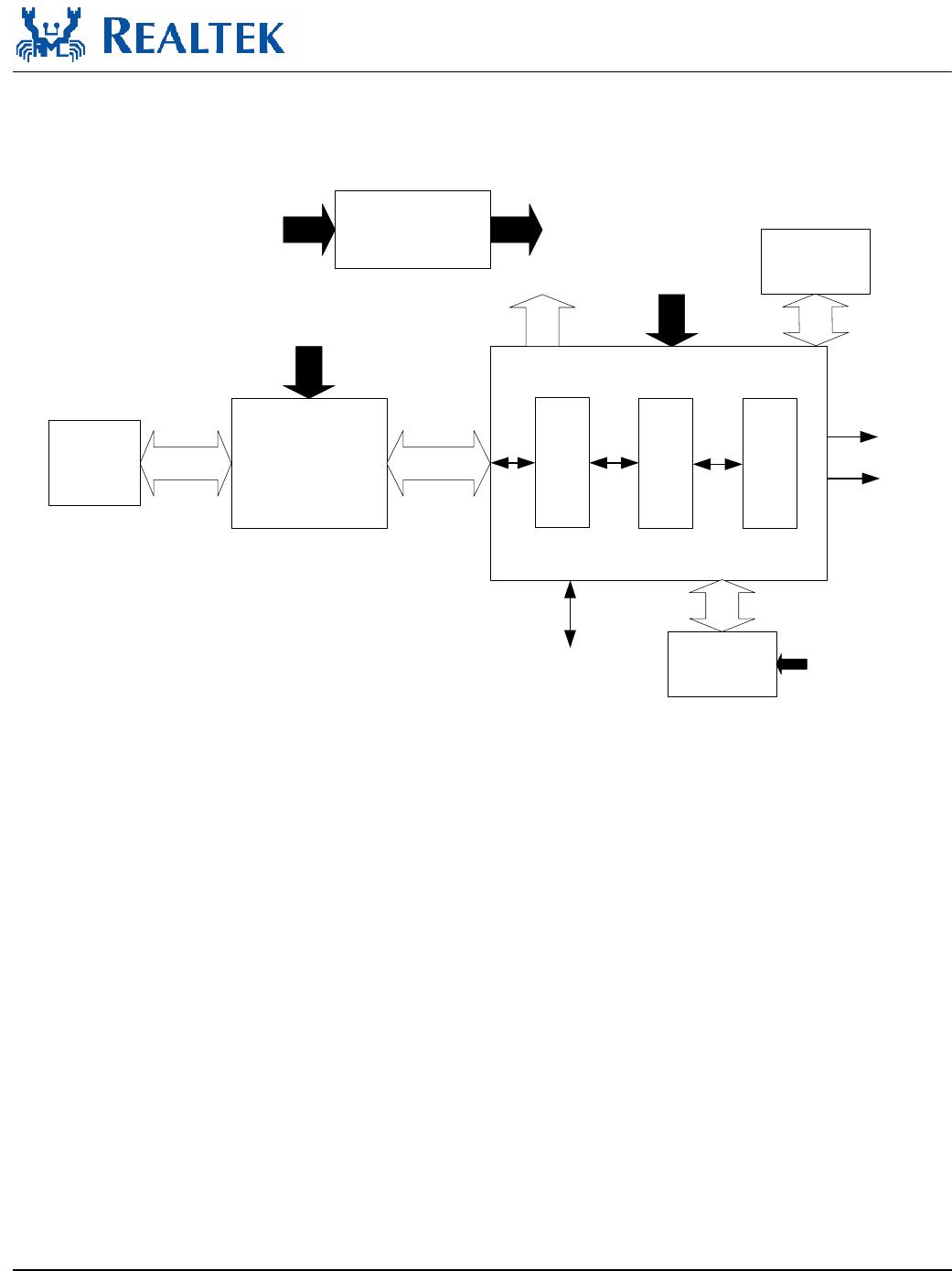
4. Block Diagram
MAC/BBP
Interface
Interrupt
Control
Logic
FIFO
Transmit/
Receive
Logic
Interface
RTS, CTS,
ACK Frame
Generator
FIFO
Control
Logic
Frame Type
Discriminator
Power and TX/RX Timing Control Logic
SIE + Register
Frame Length
Register
EEPROM
Interface LED Driver
Scrambler
TXI
MAC
BBP, TX Section
CCA/
NAV From BBP
WEP/
TKIP/
AES
Engine
Checksum
Logic
Serial
Control Radio and
Synthesizer
Control
Coding Digital
Filter TXQ
TXDET
TXAGC
TX AGC
Control
Descrambler
RXI
MAC/BBP
Interface Decoding
ADC
RXQ
DAC
RSSI
RXAGC
RX AGC
Control
ADC
ADC
Clear Channel
Assessment/
Signal Quality
Antenna
Diversity
Control
TX State
Machine
Register
From
MAC
RX State
Machine
Register
From
MAC
To MAC
D+
D-
BBP, RX Section
MAC/BBP
Interface DAC
ADC
DAC
DAC
ANTSELB
ANTSEL
Figure 1. Block Diagram
RTL8187L
Datasheet
Wireless LAN Network Interface Controller 5 Track ID JATR-1076-21 Rev. 1.2
6. Pin Descriptions
In order to reduce pin count, and therefore size and cost, some pins have multiple functions. In such cases,
the functions are separated with a ‘/’ symbol. Refer to the Pin Assignments diagram on page 4 for a
graphical representation.
The following signal type codes are used in the tables:
I: Input.
O: Output
T/S: Tri-State bi-directional input/output pin.
S/T/S: Sustained Tri-State.
O/D: Open Drain.
6.1.
USB Transceiver Interface
Table 1. USB Transceiver Interface
Symbol Type Pin No Description
HSDP I/O 26 High speed USB D+ signal
HSDM I/O 24 High speed USB D- signal
FSDP I/O 27 Full speed USB D+ signal
FSDM I/O 25 Full speed USB D- signal
RUP N/A 28 External pull-up resistor (1.5kW) for D+ line.
RREF N/A 31 External Reference. Requires 1% precision 6.25K resistor to ground
6.2.
EEPROM Interface
Table 2. EEPROM Interface
Symbol Type Pin No Description
EESK O 51 EESK in 93C46 (93C56) programming or auto-load mode.
EEDI O 39 EEDI in 93C46 (93C56) programming or auto-load mode.
EEDO I/O 36 EEDO in 93C46 (93C56) programming or auto-load mode.
EECS O 47 EEPROM Chip Select.
93C46 (93C56) chip select.
6.3.
Power Pins
Table 3. Power Pins
Symbol Type Pin No Description
VDD33 P 40, 59, 78, 93, 111 +3.3V (Digital).
AVDD P 2, 9, 22, 29, 32, 127 +3.3V (Analog).
VDD P 44, 53, 72, 82, 90, 96,
105, 115
+1.8V.
GND P 41, 45, 52, 60, 73, 80,
83, 91, 110
Ground (Digital).
AGND P 3, 10, 21, 23, 30, 123,
126, 128
Ground (Analog).

RTL8187L
Datasheet
Wireless LAN Network Interface Controller 6 Track ID JATR-1076-21 Rev. 1.2
6.4.
LED Interface
Table 4. LED Interface
Symbol Type Pin No Description
LED0, 1 O 48, 56 LED Pins (Active low)
LEDS1~0 00 01 10 11
LED0 TX/RX TX/RX TX LINK/ACT
LED1 Infrastructure LINK RX Infrastructure
During power down mode, the LED signals are logic high.
6.5.
Attachment Unit Interface
6.5.1. RTL8225 RF Chipset
Table 5. Attachment Unit Interface
Symbol Type Pin No Description
RIFSCK O 57 Serial Clock Output.
For the RTL8225 RF chipset, all operation mode switching and register setting is
done via a 4-wire serial interface.
RIFSD I/O 61 Serial Data Input/Output.
RFLE O 58 Serial Enable control.
CALEN O 77 Serial Read/Write control.
CALMODE O 108 Receiver Output.
I and Q channel AC coupling high-pass corner frequency selection. The output
function of this pin is not used in the RTL8225 RF chipset.
LNA_HL O 88 Not used in the RTL8225 RF chipset.
ANTSEL O 87 Antenna Select.
The antenna detects signal change states as the receiver switches from antenna to
antenna during the acquisition process in antenna diversity mode. This is a
complement for ANTSELB for differential drive of antenna switches.
ANTSELB O 95 Antenna Select B.
The antenna detects signal change states as the receiver switches from antenna to
antenna during the acquisition process in the antenna diversity mode. This is a
complement for ANTSEL for differential drive of antenna switches.
TRSW
TRSWB
O
O
104
103
Transmit/Receive path select.
The TRSW select signal controls the direction of the Transmit/Receive switch.
VCOPDN O 49 Output Pin as shutdown mode select digital input.
A_PAPE O 85 2.4GHz Transmit Power Amplifier Power Enable.
B_PAPE O 107 Not used in the RTL8225 RF chipset.
RFTXEN O 102 Not used in the RTL8225 RF chipset.
RFRXEN O 113 Not used in the RTL8225 RF chipset.
GPIO0 O 67 General purpose input/output pin.
GPIO1 O 68 General purpose input/output pin.
GPIO2 O 69 General purpose input/output pin.
GPIO3 O 70 General purpose input/output pin.

RTL8187L
Datasheet
Wireless LAN Network Interface Controller 7 Track ID JATR-1076-21 Rev. 1.2
Symbol Type Pin No Description
GPIO4 O 100 General purpose input/output pin.
GPIO5 O 94 General purpose input/output pin.
VREFO X 118 Not used in the RTL8225 RF chipset.
VRP X 119 Not used in the RTL8225 RF chipset.
VRN X 120 Not used in the RTL8225 RF chipset.
RXIP
RXIN
I
I
121
122
Receive (Rx) In-phase Analog Data.
RXQP
RXQN
I
I
124
125
Receive (Rx) Quadrature-phase Analog Data.
RXAGC I 4 Not used in the RTL8225 RF chipset.
TXAGC O 5 Not used in the RTL8225 RF chipset.
RSSI I 6 Analog Input to the Receive Power A/D Converter for Receive AGC Control.
TSSI0 I 7 Input to the Transmit Power A/D Converter for 2.4GHz Transmit AGC Control.
TSSI1 I 8 Not used in the RTL8225 RF chipset.
TXQP
TXQN
I
I
11
12
Not used in the RTL8225 RF chipset.
TXIP
TXIN
O
O
14
13
Not used in the RTL8225 RF chipset.
TXQTP
TXQTN
O
O
15
16
Transmit (TX) Quadrature-phase Analog Data.
TXITP
TXITN
O
O
17
18
Transmit (TX) In-phase Analog Data.
6.5.2. RTL8255 RF Chipset
Table 6. RTL8255 RF Chipset
Symbol Type Pin No Description
RIFSCK O 57 Serial Clock Output.
For the RTL8255 RF chipset, all operation mode switching and register setting is
done via a 3-wire serial interface.
RIFSD O 61 Serial Data Input/Output.
RFLE O 58 Serial Enable control.
CALEN X 77 Not used in the RTL8255 RF chipset.
CALMODE O 108 Receiver Output.
I and Q channel AC coupling high-pass corner frequency selection. The output
function of this pin is not used in the RTL8255 RF chipset.
LNAHL O 88 Not used in the RTL8255 RF chipset.
ANTSEL
ANTSELB
O
O
87
95
Antenna Select.
The antenna detects signal change states as the receiver switches from antenna to
antenna during the acquisition process in antenna diversity mode.
TRSW
TRSWB
O
O
104
103
Transmit/Receive path select.
The TRSW select signal controls the direction of the Transmit/Receive switch.
VCOPDN O 49 Not used in the RTL8255 RF chipset.
APAPE O 85 2.4GHz Transmit Power Amplifier Power Enable.
BPAPE O 107 5GHz Transmit Power Amplifier Power Enable.
RTL8187L
Datasheet
Wireless LAN Network Interface Controller 8 Track ID JATR-1076-21 Rev. 1.2
Symbol Type Pin No Description
RFTXEN O 102 Not used in the RTL8255 RF chipset.
RFRXEN O 113 Not used in the RTL8255 RF chipset.
GPIO[0] O 67 General purpose input/output pin.
GPIO[1] O 68 General purpose input/output pin.
GPIO[2] O 69 General purpose input/output pin.
GPIO[3] O 70 General purpose input/output pin.
GPIO[4] O 100 General purpose input/output pin.
GPIO[5] O 94 General purpose input/output pin.
VREFO X
118 Not used in the RTL8255 RF chipset.
VRP X 119 Not used in the RTL8255 RF chipset.
VRN X 120 Not used in the RTL8255 RF chipset.
RXIP
RXIN
I
I
121
122
Receive (Rx) In-phase Analog Data.
RXQP
RXQN
I
I
124
125
Receive (Rx) Quadrature-phase Analog Data.
RXAGC O 4 Not used in the RTL8255 RF chipset.
TXAGC O 5 Not used in the RTL8255 RF chipset.
RSSI I 6 Analog Input to the Receive Power A/D Converter for Receive AGC Control.
TSSI0 I 7 Input to the Transmit Power A/D Converter for 2.4GHz Transmit AGC Control.
TSSI1 I 8 Input to the Transmit Power A/D Converter for 5GHz Transmit AGC Control.
TXQP
TXQN
O
O
11
12
Transmit (TX) Quadrature-phase Analog Data.
TXIP
TXIN
O
O
14
13
Transmit (TX) In-phase Analog Data.
TXQTP
TXQTN
O
O
15
16
Not used in the RTL8255 RF chipset.
TXITP
TXITN
O
O
17
18
Not used in the RTL8255 RF chipset.
6.6.
Clock and Other Pins
Table 7. Clock and Other Pins
Symbol Type Pin No Description
R15K I/O 1 This pin must be pulled low by a 15K Ω resistor.
XI I 20 40MHz OSC Input.

RTL8187L
Datasheet
Wireless LAN Network Interface Controller 9 Track ID JATR-1076-21 Rev. 1.2
7. CPU Access to Endpoint Data
7.1.
Control Transfer
Control transfers configure and send commands to a device. Because they are so important, they employ
extensive USB error checking. The host reserves a portion of each USB frame for control transfers. Control
transfers consist of two or three stages. The SETUP stage contains eight bytes of USB control data. An
optional DATA stage contains more data, if required. The STATUS stage allows the device to indicate
successful completion of a control operation.
7.2.
Bulk Transfer
Bulk data is bursty, traveling in packets of 8, 16, 32, or 64 bytes at full speed, or at 512 bytes at high speed.
Bulk data has guaranteed accuracy due to an automatic retry mechanism for erroneous data. The host
schedules bulk packets when there is available bus time.
RTL8187L
Datasheet
Wireless LAN Network Interface Controller 10 Track ID JATR-1076-21 Rev. 1.2
8. USB Request
8.1.
Get Descriptor-Device
Table 8. Get Descriptor-Device
Setup Transaction
BmReq bReq wValueL wValueH wIndexL wIndexH wLengthL wLengthH
80 06 00 01 00 00 Lengh_L Length_H
High Speed Data Transaction
DATA0 DATA1 DATA2 DATA3 DATA4 DATA5 DATA6 DATA7
12 01 00 02 00 00 00 40
DA 0B 87 81 00 01 01 02
03 01
Full Speed Data Transaction
DATA0 DATA1 DATA2 DATA3 DATA4 DATA5 DATA6 DATA7
12 01 10 01 00 00 00 40
DA 0B 87 81 00 01 01 02
03 01
8.2.
Get Descriptor-Device Qualifier (High Speed)
Table 9. Get Descriptor- Device Qualifier (High Speed)
Setup Transaction
BmReq bReq wValueL wValueH wIndexL wIndexH wLengthL wLengthH
80 06 00 06 00 00 Lengh_L Length_H
Data Transaction
DATA0 DATA1 DATA2 DATA3 DATA4 DATA5 DATA6 DATA7
0A 06 00 02 00 00 00 40
01 00
RTL8187L
Datasheet
Wireless LAN Network Interface Controller 11 Track ID JATR-1076-21 Rev. 1.2
8.3.
Get Descriptor-Configuration
Table 10. Get Descriptor-Configuration
Setup Transaction
BmReq bReq wValueL wValueH wIndexL wIndexH wLengthL wLengthH
80 06 00 02 00 00 Lengh_L Length_H
High Speed Data Transaction
DATA0 DATA1 DATA2 DATA3 DATA4 DATA5 DATA6 DATA7
09 02 27 00 01 01 04 80
FA 09 04 00 00 03 00 00
00 05 07 05 81 02 00 02
00 07 05 02 02 00 02 00
07 05 03 02 00 02 00
Full Speed Data Transaction
DATA0 DATA1 DATA2 DATA3 DATA4 DATA5 DATA6 DATA7
09 02 27 00 01 01 00 E0
01 09 04 00 00 03 00 00
00 05 07 05 81 02 40 00
00 07 05 02 02 40 00 00
07 05 03 02 40 00 00
8.4.
Get Descriptor-String Index 0
Table 11. Get Descriptor-String Index 0
Setup Transaction
BmReq bReq wValueL wValueH wIndexL wIndexH wLengthL wLengthH
80 06 00 03 00 00 Lengh_L Length_H
Data Transaction
DATA0 DATA1 DATA2 DATA3 DATA4 DATA5 DATA6 DATA7
04 03 09 04 - - - -
RTL8187L
Datasheet
Wireless LAN Network Interface Controller 12 Track ID JATR-1076-21 Rev. 1.2
8.5.
Get Descriptor-String Index 1
Table 12. Get Descriptor-String Index 1
Setup Transaction
BmReq bReq wValueL wValueH wIndexL wIndexH wLengthL wLengthH
80 06 01 03 09 04 Lengh_L Length_H
Data Transaction
DATA0 DATA1 DATA2 DATA3 DATA4 DATA5 DATA6 DATA7
10 03 52 00 65 00 61 00
6C 00 74 00 65 00 6B 00
8.6.
Get Descriptor-String Index 2
Table 13. Get Descriptor-String Index 2
Setup Transaction
BmReq bReq wValueL wValueH wIndexL wIndexH wLengthL wLengthH
80 06 02 03 09 04 Lengh_L Length_H
Data Transaction
DATA0 DATA1 DATA2 DATA3 DATA4 DATA5 DATA6 DATA7
3A 03 52 00 54 00 4C 00
38 00 31 00 38 00 37 00
20 00 57 00 59 00 72 00
65 00 6C 00 65 00 73 00
73 00 20 00 4C 00 41 00
4E 00 20 00 41 00 64 00
61 00 70 00 74 00 65 00
72 00
RTL8187L
Datasheet
Wireless LAN Network Interface Controller 13 Track ID JATR-1076-21 Rev. 1.2
8.7.
Get Descriptor-String Index 3
Table 14. Get Descriptor-String Index 3
Setup Transaction
BmReq bReq wValueL wValueH wIndexL wIndexH wLengthL wLengthH
80 06 03 03 09 04 Lengh_L Length_H
Data Transaction
DATA0 DATA1 DATA2 DATA3 DATA4 DATA5 DATA6 DATA7
1A 03 30 00 30 00 65 00
30 00 34 00 63 00 30 00
30 00 30 00 30 00 30 00
31 00
8.8.
Get Descriptor-String Index 4
Table 15. Get Descriptor-String Index 4
Setup Transaction
BmReq bReq wValueL wValueH wIndexL wIndexH wLengthL wLengthH
80 06 04 03 09 04 Lengh_L Length_H
Data Transaction
DATA0 DATA1 DATA2 DATA3 DATA4 DATA5 DATA6 DATA7
2C 03 57 00 69 00 72 00
65 00 6C 00 65 00 73 00
73 00 20 00 4E 00 65 00
74 00 77 00 6F 00 72 00
6B 00 20 00 43 00 61 00
72 00 64 00
RTL8187L
Datasheet
Wireless LAN Network Interface Controller 14 Track ID JATR-1076-21 Rev. 1.2
8.9.
Get Descriptor-String Index 5
Table 16. Get Descriptor-String Index 5
Setup Transaction
BmReq bReq wValueL wValueH wIndexL wIndexH wLengthL wLengthH
80 06 05 03 09 04 Lengh_L Length_H
Data Transaction
DATA0 DATA1 DATA2 DATA3 DATA4 DATA5 DATA6 DATA7
34 03 42 00 75 00 6C 00
6B 00 2D 00 49 00 4E 00
2C 00 42 00 75 00 6C 00
6B 00 2D 00 4F 00 55 00
54 00 2C 00 42 00 75 00
6C 00 6B 00 2D 00 4F 00
55 00 54 00
8.10.
Get Descriptor-Other Speed Configuration
Table 17. Get Descriptor-Other Speed Configuration
Setup Transaction
BmReq bReq wValueL wValueH wIndexL wIndexH wLengthL wLengthH
80 06 00 07 00 00 Lengh_L Length_H
High Speed Data Transaction
DATA0 DATA1 DATA2 DATA3 DATA4 DATA5 DATA6 DATA7
09 02 27 00 01 01 04 80
FA 09 04 00 00 03 00 00
00 05 07 05 81 02 00 02
00 07 05 02 02 00 02 00
07 05 03 02 00 02 00
Full Speed Data Transaction
DATA0 DATA1 DATA2 DATA3 DATA4 DATA5 DATA6 DATA7
09 02 27 00 01 01 00 E0
01 09 04 00 00 03 00 00
00 05 07 05 81 02 40 00
00 07 05 02 02 40 00 00
07 05 03 02 40 00 00

RTL8187L
Datasheet
Wireless LAN Network Interface Controller 15 Track ID JATR-1076-21 Rev. 1.2
8.11.
Set Address
Table 18. Set Address
Setup Transaction
BmReq bReq wValueL wValueH wIndexL wIndexH wLengthL wLengthH
00 05 addrL addrH 00 00 00 00
Note: No data transaction.
8.12.
Set Interface 0
Table 19. Set Interface 0
Setup Transaction
BmReq bReq wValueL wValueH wIndexL wIndexH wLengthL wLengthH
01 0B 00 00 00 00 00 00
Note: No data transaction.
8.13.
Set Feature Device
Table 20. Set Feature Device
Setup Transaction
BmReq bReq wValueL wValueH wIndexL wIndexH wLengthL wLengthH
00 03 01 00 00 00 00 00
Note: No data transaction.

RTL8187L
Datasheet
Wireless LAN Network Interface Controller 16 Track ID JATR-1076-21 Rev. 1.2
8.14.
Clear Feature Device
Table 21. Clear Feature Device
Setup Transaction
BmReq bReq wValueL wValueH wIndexL wIndexH wLengthL wLengthH
00 01 01 00 00 00 00 00
Note: No data transaction.
8.15.
Set Config 0
Table 22. Set Config 0
Setup Transaction
BmReq bReq wValueL wValueH wIndexL wIndexH wLengthL wLengthH
00 09 00 02 00 00 00 00
Note: No data transaction.
8.16.
Set Config 1
Table 23. Set Config 1
Setup Transaction
BmReq bReq wValueL wValueH wIndexL wIndexH wLengthL wLengthH
00 09 01 00 00 00 00 00
Note: No data transaction.

RTL8187L
Datasheet
Wireless LAN Network Interface Controller 17 Track ID JATR-1076-21 Rev. 1.2
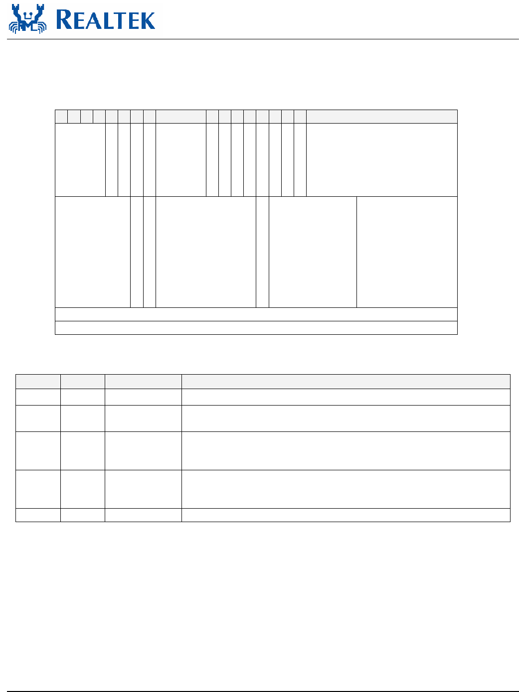
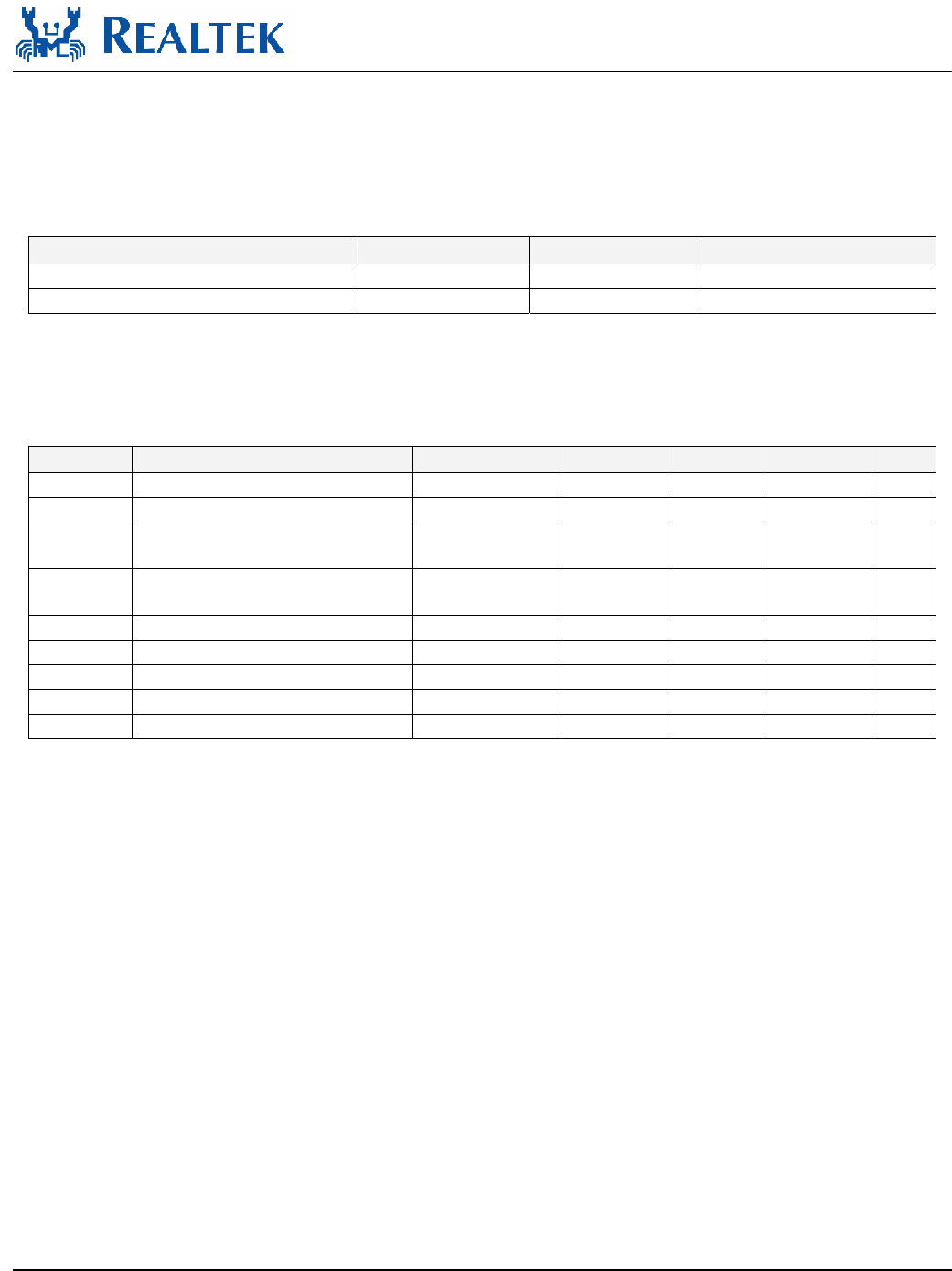
9. EEPROM (93C46 or 93C56) Contents
The RTL8187L supports the attachment of an external EEPROM. The 93C46 is a 1Kbit EEPROM (the
93C56 is a 2Kbit EEPROM). The EEPROM interface provides the ability for the RTL8187L to read from,
and write data to, an external serial EEPROM device. If the EEPROM is not present, the RTL8187L
initialization uses default values for the Operational Registers. Software can read and write to the
EEPROM using “bit-bang” accesses via the 9346CR Register.
Although it is actually addressed by words, its contents are listed below by bytes for convenience. After the
initial power on or auto-load command in the 9346CR, the RTL8187L performs a series of EEPROM read
operations from the 93C46 (93C56).
Note: It is suggested to obtain Realtek approval before changing the default settings of the EEPROM.
Table 24. EEPROM (93C46 or 93C56) Contents
Bytes Contents Description
00h 87h
01h 81h
These 2 bytes contain the ID code word for the RTL8187L. The RTL8187L will load
the contents of the EEPROM into the corresponding location if the ID word (8187h) is
correct.
02h-03h VID USB Vendor ID.
04h-05h DID USB Device ID.
06h ChannelPlan Channel Plan: Map of channels to be scanned.
07h EnergyDetThr Energy detection threshold.
08h RFParm RF specific parameter.
09h-0Ah Version The version of EEPROM content.
0Bh Options function Bit0: Timeout function.
0: Disable RTL8187L’s USB timeout mechanism.
1: Enable RTL8187L’s USB timeout mechanism.
Bit1: USB remote wake up function.
0: There is no remote wake up feature for the RTL8187L.
1: There is a remote wake up feature for the RTL8187L.
Bit2:
0: The RTL8187L’s remote wake-up is based on the WLAN’s wake-up signal
1: The RTL8187L’s remote wake-up is push-button based.
Bit3: USB Status stage.
1: Bypass the check setup interrupt procedure of 8051 when host sends set_address
command.
Bit4: SelfloopbackISR function.
1: The UTM self loopback will be initialized by internal 8051.
Bit7:
1: The power control signal to AFE will be auto controlled by suspendm.
0Ch RFChipID RF Chip ID.
The identifier of the RF chip.

RTL8187L
Datasheet
Wireless LAN Network Interface Controller 18 Track ID JATR-1076-21 Rev. 1.2
Bytes Contents Description
0Dh CONFIG3 RTL8187L Configuration register 3.
Operational register FF59h.
0Eh~13h MAC Address MAC Address.
After the auto-load command or a hardware reset, the RTL8187L loads MAC
Addresses to IDR0~IDR5 of the I/O registers of the RTL8187L.
14h - Reserved.
15h CONFIG1 RTL8187L Configuration register 1.
Operational register FF52h.
16h~17h CRC 16-bit CRC value of EEPROM content.
18h CONFIG2 RTL8187L Configuration register 2.
Operational register FF53h.
19h CONFIG4 RTL8187L Configuration register 4.
Operational register FF5Ah.
1Ah~1Dh ANA_PARM Analog Parameter for the RTL8187L.
Operational registers of the RTL8187L are from FF54h to FF57h.
Reserved. Do not change this field without Realtek approval.
1Eh TESTR RTL8187L Test Mode Register.
Operational register FF5Bh.
Reserved. Do not change this field without Realtek approval.
1Fh - Reserved.
20h OFDM_TxPower
1
Transmit Power Level for 802.11a-defined channel_ID 36
(Center frequency=5180MHz).
21h OFDM_TxPower
2
Transmit Power Level for 802.11a-defined channel_ID 40
(Center frequency=5200MHz).
22h OFDM_TxPower
3
Transmit Power Level for 802.11a-defined channel_ID 44
(Center frequency=5220MHz).
23h OFDM_TxPower
4
Transmit Power Level for 802.11a-defined channel_ID 48
(Center frequency=5240MHz).
24h OFDM_TxPower
5
Transmit Power Level for 802.11a-defined channel_ID 52
(Center frequency=5260MHz).
25h OFDM_TxPower
6
Transmit Power Level for 802.11a-defined channel_ID 56
(Center frequency=5280MHz).
26h OFDM_TxPower
7
Transmit Power Level for 802.11a-defined channel_ID 60
(Center frequency=5300MHz).
27h OFDM_TxPower
8
Transmit Power Level for 802.11a-defined channel_ID 64
(Center frequency=5320MHz).
28h OFDM_TxPower
9
Transmit Power Level for 802.11a-defined channel_ID 149
(Center frequency=5745MHz).
29h OFDM_TxPower
10
Transmit Power Level for 802.11a-defined channel_ID 153
(Center frequency=5765MHz).
2Ah OFDM_TxPower
11
Transmit Power Level for 802.11a-defined channel_ID 157
(Center frequency=5785MHz).
2Bh OFDM_TxPower
12
Transmit Power Level for 802.11a-defined channel_ID 161
(Center frequency=5805MHz).
2Ch CCK_TxPower1 Transmit Power Level for 802.11b(g)-defined channel_ID 1
(center frequency=2412MHz).

RTL8187L
Datasheet
Wireless LAN Network Interface Controller 19 Track ID JATR-1076-21 Rev. 1.2
Bytes Contents Description
2Dh CCK_TxPower2 Transmit Power Level for 802.11b(g)-defined channel_ID 2
(center frequency=2417MHz).
2Eh CCK_TxPower3 Transmit Power Level for 802.11b(g)-defined channel_ID 3
(center frequency=2422MHz).
2Fh CCK_TxPower4 Transmit Power Level for 802.11b(g)-defined channel_ID 4
(center frequency=2427MHz).
30h CCK_TxPower5 Transmit Power Level for 802.11b(g)-defined channel_ID 5
(center frequency=2432MHz).
31h CCK_TxPower6 Transmit Power Level for 802.11b(g)-defined channel_ID 6
(center frequency=2437MHz).
32h-35h ANA_PARM2 Reserved: Do not change this field without Realtek approval.
Analog Parameter1 for the RTL8187L: Operational registers of the RTL8187L are
from FF60h to FF63h.
36h CCK_TxPower11 Transmit Power Level for 802.11b(g)-defined channel_ID 11
(center frequency=2462MHz).
37h CCK_TxPower12 Transmit Power Level for 802.11b(g)-defined channel_ID 12
(center frequency=2467MHz).
38h CCK_TxPower13 Transmit Power Level for 802.11b(g)-defined channel_ID 13
(center frequency=2472MHz).
39h CCK_TxPower14 Transmit Power Level for 802.11b(g)-defined channel_ID 14
(center frequency=2484MHz).
3Ah-6Bh Manufacture String
&
Product String
Manufacture String and Product String:Those bits specify both manufacturer’s
information and device’s information for the USB standard request.
Maximum two strings total length are 50 bytes.
6Ch-79h - Reserved.
7Ah CCK_TxPower7 Transmit Power Level for 802.11b(g)-defined channel_ID 7
(center frequency=2442MHz).
7Bh CCK_TxPower8 Transmit Power Level for 802.11b(g)-defined channel_ID 8
(center frequency=2447MHz).
7Ch CCK_TxPower9 Transmit Power Level for 802.11b(g)-defined channel_ID 9
(center frequency=2452MHz).
7Dh CCK_TxPower10 Transmit Power Level for 802.11b(g)-defined channel_ID 10
(center frequency=2457MHz).
RTL8187L
Datasheet
Wireless LAN Network Interface Controller 20 Track ID JATR-1076-21 Rev. 1.2
9.1.
EEPROM Registers Summary
Table 25. EEPROM Registers Summary
Address Name Type Bit7 Bit6 Bit5 Bit4 Bit3 Bit2 Bit1 Bit0
FF00h-
FF05h IDR0 – IDR5 R/W*
R LEDS1 LEDS0 - LWACT - - - -
FF52h CONFIG1 W* LEDS1 LEDS0 - LWACT - - - -
R LCK - - - -
PAPE
_sign
PAPE
_time
FF53h CONFIG2
W* - - - - -
PAPE
_sign
PAPE
_time
FF54h-
FF57h ANA_PARM R/W** 32-bit Read Write
R - PARM_En Magic - - - - -
FF59h CONFIG3 W* - PARM_En Magic - - - - -
R - - - LWPME - LWPTN -
FF5Ah CONFIG4 W* - - - LWPME - LWPTN -
FF5Bh TESTR 8-bit Read Write
FF60h-
FF63h ANA_PARM2 R/W 32-bit Read Write
FFD8h CONFIG5 R/W** - - - - - - LANWake -
Note 1: Registers marked 'W*' can be written only if bits EEM1=EEM0=1.
Note 2: Registers marked 'W**' can be written only if bits EEM1:0=[1:1] and
CONFIG3<PARM_EN>= 0.
9.2.
EEPROM Power Management Registers Summary
Table 26. EEPROM Power Management Registers Summary
Configuration
Space Offset
Name Type Bit7 Bit6 Bit5 Bit4 Bit3 Bit2 Bit1 Bit0
52h R Aux_I_b1 Aux_I_b0 DSI Reserved PMECLK Version
53h
PMC
R PME_D3cold PME_D3hot PME_D2 PME_D1 PME_D0 D2 D1 Aux_I_b2

RTL8187L
Datasheet
Wireless LAN Network Interface Controller 21 Track ID JATR-1076-21 Rev. 1.2
10. USB Packet Buffering
The RTL8187L incorporates two independent FIFOs for transferring data to/from the system interface and
from/to the network. The FIFOs provide temporary storage of data, freeing the host system from the
real-time demands of the network.
The way in which the FIFOs are emptied and filled is controlled by the FIFO threshold values in the
Receive Configuration registers. These values determine how full or empty the FIFOs must be before the
device requests the bus. Once the RTL8187L requests the bus, it will attempt to empty or fill the FIFOs as
allowed by the respective MXDMA settings in the Transmit Configuration and Receive Configuration
registers.
10.1.
Transmit Buffer Manager
The buffer management scheme used on the RTL8187L allows quick, simple, and efficient use of the frame
buffer memory. The buffer management scheme uses separate buffers and descriptors for packet
information. This allows effective transfers of data to the transmit buffer manager by simply transferring
the descriptor information to the transmit queue.
The Tx Buffer Manager DMA’s packet data from system memory and places it in the 3.5KB transmit FIFO,
and pulls data from the FIFO to send to the Tx MAC. Multiple packets may be present in the FIFO,
allowing packets to be transmitted with Short InterFrame (SIF) space. Additionally, once the RTL8187L
requests the bus, it will attempt to fill the FIFO as allowed by the MXDMA setting.
The Tx Buffer Manager process also supports priority queuing of transmit packets. It handles this by
drawing from two separate descriptor lists to fill the internal FIFO. If packets are available in the high
priority queues, they will be loaded into the FIFO before those of low priority.
10.2.
Receive Buffer Manager
The Rx Buffer Manager uses the same buffer management scheme as used for transmits. The Rx Buffer
Manager retrieves packet data from the Rx MAC and places it in the 4KB receive data FIFO, and pulls data
from the FIFO for DMA to system memory. The receive FIFO is controlled by the FIFO threshold value in
RXFTH. This value determines the number of long words written into the FIFO from the MAC unit before
a DMA request for system memory occurs. Once the RTL8187L gets the bus, it will continue to transfer the
long words from the FIFO until the data in the FIFO is less than one long word, or has reached the end of the
packet, or the max DMA burst size is reached, as set in MXDMA.
10.3.
Packet Recognition
The Rx packet filter and recognition logic allows software to control which packets are accepted, based on
destination address and packet type. Address recognition logic includes support for broadcast, multicast
hash, and unicast addresses. The packet recognition logic includes support for WOL and programmable
pattern recognition.
RTL8187L
Datasheet
Wireless LAN Network Interface Controller 22 Track ID JATR-1076-21 Rev. 1.2
11. Functional Description
11.1.
Transmit & Receive Operations
The RTL8187L supports a new descriptor-based buffer management that will significantly lower host CPU utilization. The
RTL8187L supports transmit descriptor and receive descriptor in memory. Each OUT packet contains 3-double-word transmit
descriptors and each IN packet contains 4-double-word receive descriptors.
11.1.1. Transmit
Tx Descriptor Format
Table 27. Tx Descriptor Format
31 30 29 28 27 26 25 24 23 22 21 20 19 18 17 16 15 14 13 12 11 10 9 8 7 6 5 4 3 2 1 0
RSVD
TXRATE
(4 bits)
R
T
S
E
N
RTSRATE
(4 bits)
C
T
S
E
N
M
O
R
E
F
R
A
G
S
P
L
C
P
N
O
_
E
N
C
R
Y
P
T
RSVD
TPKTSIZE (12 bits) Offset 0
L
E
N
G
E
X
T
Length (15 bits)
RTSDUR (16 bits)
Offset 4
RATE_
FALL
BACK_
LIMIT
(4 bits)
R
S
V
D
(3 bits)
A
N
T
E
N
N
A
AGC (8 bits) RETRY_LIMIT (8 bits) CWMAX
(4 bits)
CWMIN
(4 bits)
Offset 8
RTL8187L
Datasheet
Wireless LAN Network Interface Controller 23 Track ID JATR-1076-21 Rev. 1.2
Table 28. Tx Status Descriptor
Offset# Bit# Symbol Description
0 31:28 RSVD Reserved.
Tx Rate.
These four bits indicate the current frame’s transmission rate.
Bit 27 Bit 26 Bit 25 Bit 24
1Mbps 0 0 0 0
2Mbps 0 0 0 1
5.5Mbps 0 0 1 0
11Mbps 0 0 1 1
6Mbps 0 1 0 0
9Mbps 0 1 0 1
12Mbps 0 1 1 0
18Mbps 0 1 1 1
24Mbps 1 0 0 0
36Mbps 1 0 0 1
48Mbps 1 0 1 0
54Mbps 1 0 1 1
Reserved All other combinations
0 27:24 TXRATE
0 23 RTSEN RTS Enable.
Set to 1 indicates that an RTS/CTS handshake shall be performed at the
beginning of any frame exchange sequence where the frame is of type Data or
Management, the frame has a unicast address in the Address1 field, and the
length of the frame is greater than RTSThreshold.
RTS Rate.
These four bits indicate the RTS frame’s transmission rate before transmitting the
current frame and will be ignored if the RTSEN bit is set to 0.
Bit 22 Bit 21 Bit 20 Bit 19
1Mbps 0 0 0 0
2Mbps 0 0 0 1
5.5Mbps 0 0 1 0
11Mbps 0 0 1 1
6Mbps 0 1 0 0
9Mbps 0 1 0 1
12Mbps 0 1 1 0
18Mbps 0 1 1 1
24Mbps 1 0 0 0
36Mbps 1 0 0 1
48Mbps 1 0 1 0
54Mbps 1 0 1 1
Reserved All other combinations
0 22:19 RTSRATE
0 18 CTSEN CTS Enable.
Both RTSEN and CTSEN set to 1 indicates that the CTS-to-Self protection
mechanism will be used.

RTL8187L
Datasheet
Wireless LAN Network Interface Controller 24 Track ID JATR-1076-21 Rev. 1.2
Offset# Bit# Symbol Description
0 17 MOREFRAG More Fragment.
This bit is set to 1 in all data type frames that have another fragment of the current
packet to follow.
0 16 SPLCP Short Physical Layer Convergence Protocol format.
When set, this bit indicates that a short PLCP preamble will be added to the
header before transmitting the frame.
0 15 NO_ENCRYPT No Encryption.
This packet will be sent out without encryption even if Tx encryption is enabled.
0 14:12 RSVD Reserved.
0 11:0 TPKTSIZE Transmit Packet Size.
This field indicates the number of bytes required to transmit the frame.
4 31 LENGEXT Length Extension.
This bit is used to supplement the Length field (bits 30:16, offset 4). This bit will
be ignored if the TXRATE is set to 1Mbps, 2Mbps, or 5.5Mbps.
4 30:16 Length PLCP Length.
The PLCP length field indicates the number of microseconds required to transmit
the frame.
4 15:0 RTSDUR RTS Duration.
These bits indicate the RTS frame’s duration field before transmitting the current
frame and will be ignored if the RTSEN bit is set to 0.
8 31:28 RATE_FALL
BACK_LIMIT
Data Rate Auto Fallback Limit.
8 27:25 RSVD Reserved.
8 24 ANTENNA Tx Antenna.
8 23:16 AGC Tx AGC.
8 15:8 RETRY_LIMIT Retry Count Limit.
8 7:4 CWMAX Maximum Contention Window.
8 3:0 CWMIN Minimum Contention Window.
RTL8187L
Datasheet
Wireless LAN Network Interface Controller 25 Track ID JATR-1076-21 Rev. 1.2
11.1.2. Receive
Rx Descriptor Format
Table 29. Rx Descriptor Format
31 30 29 28 27 26 25 24 23 22 21 20 19 18 17 16 15 14 13 12 11 10 9 8 7 6 5 4 3 2 1 0
RSVD
D
M
A
F
F
O
V
F
S
P
L
C
P
R
S
V
D
RXRATE
(4 bits)
R
S
V
D
M
A
R
P
A
M
B
A
R
R
E
S
P
W
R
M
G
T
C
R
C
3
2
I
C
V
Frame_Length (12 bits)
Offset 0
RSVD (6 bits)
W
A
K
E
U
P
D
E
C
R
Y
P
T
E
D
AGC (8 bits)
A
N
T
E
N
N
A
RSSI
(7 bits)
SQ
(8 bits)
Offset 4
TSFTL Offset 8
TSFTH Offset 12
Table 30. Rx Status Descriptor
Offset# Bit# Symbol Description
0 31:28 RSVD Reserved.
0 27 DMAF RX DMA Fail.
When set, this packet will be dropped by software.
0 26 FOVF FIFO Overflow.
When set, this bit indicates that the receive FIFO was exhausted before this
packet was fully received.
0 25 SPLCP Short Physical Layer Convergence Protocol format.
When set, this bit indicates that a short PLCP preamble was added to the current
received frame.
0 24 RSVD Reserved.

RTL8187L
Datasheet
Wireless LAN Network Interface Controller 26 Track ID JATR-1076-21 Rev. 1.2
Offset# Bit# Symbol Description
Rx Rate.
These four bits indicate the current frame’s receiving rate.
Bit 23 Bit 22 Bit 21 Bit 20
1Mbps 0 0 0 0
2Mbps 0 0 0 1
5.5Mbps 0 0 1 0
11Mbps 0 0 1 1
6Mbps 0 1 0 0
9Mbps 0 1 0 1
12Mbps 0 1 1 0
18Mbps 0 1 1 1
24Mbps 1 0 0 0
36Mbps 1 0 0 1
48Mbps 1 0 1 0
54Mbps 1 0 1 1
0 23:20 RXRATE
Reserved All other combinations
0 19 RSVD Reserved.
0 18 MAR Multicast Address Packet Received.
When set, this bit indicates that a multicast packet was received.
0 17 PAM Physical Address Matched.
When set, this bit indicates that the destination address of this Rx packet matches
the value in the RTL8187L’s ID registers.
0 16 BAR Broadcast Address Received.
When set, this bit indicates that a broadcast packet was received. BAR and MAR
will not be set simultaneously.
0 15 RES Receive Error.
Valid if DMAF=0
0 14 PWRMGT Receive Power Management Packet.
When set, this bit indicates that the Power Management bit is set on the received
packet.
0 13 CRC32 CRC32 Error.
When set, this bit indicates that a CRC32 error has occurred on the received
packet. A CRC32 packet can be received only when RCR_ACRC32 is set.
0 12 ICV Integrity Check Value Error.
When set, this bit indicates that an ICV error has occurred on the received packet.
A ICV packet can be received only when RCR_AICV is set.
0 11:0 Frame_Length This bit indicates the received packet length including CRC32, in bytes.
4 31:26 RSVD Reserved.
4 25 WAKEUP The received packet is a unicast wakeup packet.
4 24 DECRYPTED The received packet has been decrypted.
4 23:16 AGC The AGC of the received packet.
4 15 ANTENNA The received packet is received through this antenna.
4 14:8 RSSI Received Signal Strength Indicator.
The RSSI is a measure of the RF energy received by the PHY.

RTL8187L
Datasheet
Wireless LAN Network Interface Controller 27 Track ID JATR-1076-21 Rev. 1.2
Offset# Bit# Symbol Description
4 7:0 SQ Signal Quality.
The SQ is a measure of the quality of BAKER code lock, providing an effective
measure during the full reception of a PLCP preamble and header.
8 31:0 TSFTL A snapshot of the TSFTR’s least significant 32 bits.
12 31:0 TSFTH A snapshot of the TSFTR’s most significant 32 bits.
11.2.
Loopback Operation
Loopback mode is normally used to verify that the logic operations have performed correctly. In loopback
mode, the RTL8187L takes frames from the transmit descriptor and transmits them up to internal Rx logic.
The loopback function does not apply to an external PHYceiver.
11.3.
Tx Encapsulation (With RTL8187L Internal Baseband
Processor)
While operating in Tx mode, the RTL8187L encapsulates the frames that it transmits according to the
Differential Binary Phase Shift Keying (DBPSK) for 1Mbps, Differential Quaternary Phase Shift Keying
(DQPSK) for 2Mbps, and Complementary Code Keying (CCK) for 5.5Mbps and 11Mbps modulators. The
changes to the original packet data are as follows:
1. The PLCP preamble is always transmitted as the DBPSK waveform and used by the receiver to achieve
initial PN synchronization.
2. The PLCP header can be configured to be either DBPSK or DQPSK and includes the necessary data
fields of the communications protocol to establish the physical layer link.
3. The MAC frame can be configured for DBPSK, DQPSK, or CCK.
11.4.
Rx Decapsulation (With RTL8187L Internal Baseband
Processor)
The RTL8187L continuously monitors the network when reception is enabled. When activity is recognized
it starts to process the incoming data. After detecting receive activity on the channel, the RTL8187L starts
to process the PLCP preamble and header based on the mode of operation.
The RTL8187L checks CRC16 and CRC32, then reports if CRC16 or CRC32 has errors. When using the
40-bit WEP and 104-bit WEP module for decryption, the RTL8187L also checks the Integrity Check Value
(ICV) and reports if the ICV has errors.
RTL8187L
Datasheet
Wireless LAN Network Interface Controller 28 Track ID JATR-1076-21 Rev. 1.2
11.5.
LED Functions
The RTL8187L supports 2 LED signals in 4 configurable operation modes. The following sections describe
the different LED actions.
11.5.1. Link Monitor
The Link Monitor senses the link integrity. Whenever link status is established, the specific link LED pin is
driven low.
11.5.2. Infrastructure Monitor
The Infrastructure Monitor senses the link integrity of an Infrastructure network. Whenever Link OK in
Infrastructure network status is established, the specific Infrastructure LED pin is driven low.
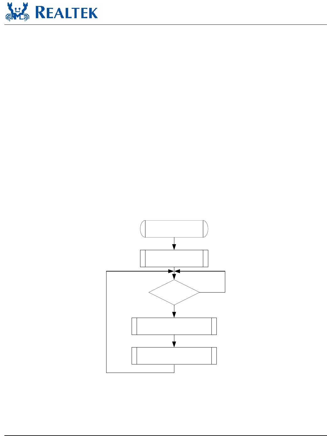
11.5.3. Rx LED
Blinking of the Rx LED indicates that receive activity is occurring.
Power On
Receiving
Packet?
LED = High
LED = High for (100 +- 10) ms
LED = Low for (12 +- 2) ms
No
Yes
Figure 3. Rx LED
RTL8187L
Datasheet
Wireless LAN Network Interface Controller 29 Track ID JATR-1076-21 Rev. 1.2
11.5.4. Tx LED
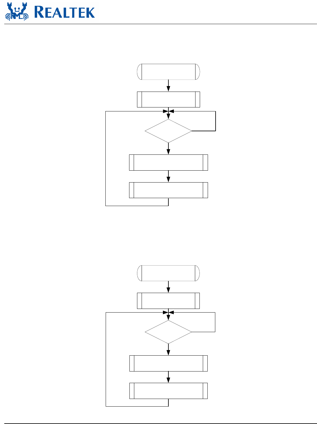
Blinking of the Tx LED indicates that transmit activity is occurring.
Power On
Transmitting
Packet?
LED = High
LED = High for (100 +- 10) ms
LED = Low for (12 +- 2) ms
No
Yes
Figure 4. Tx LED
11.5.5. Tx/Rx LED
Blinking of the Tx/Rx LED indicates that both transmit and receive activity is occurring.
Power On
Tx/Rx Packet?
LED = High
LED = High for (100 +- 10) ms
LED = Low for (12 +- 2) ms
No
Yes
Figure 5. Tx/Rx LED
RTL8187L
Datasheet
Wireless LAN Network Interface Controller 30 Track ID JATR-1076-21 Rev. 1.2
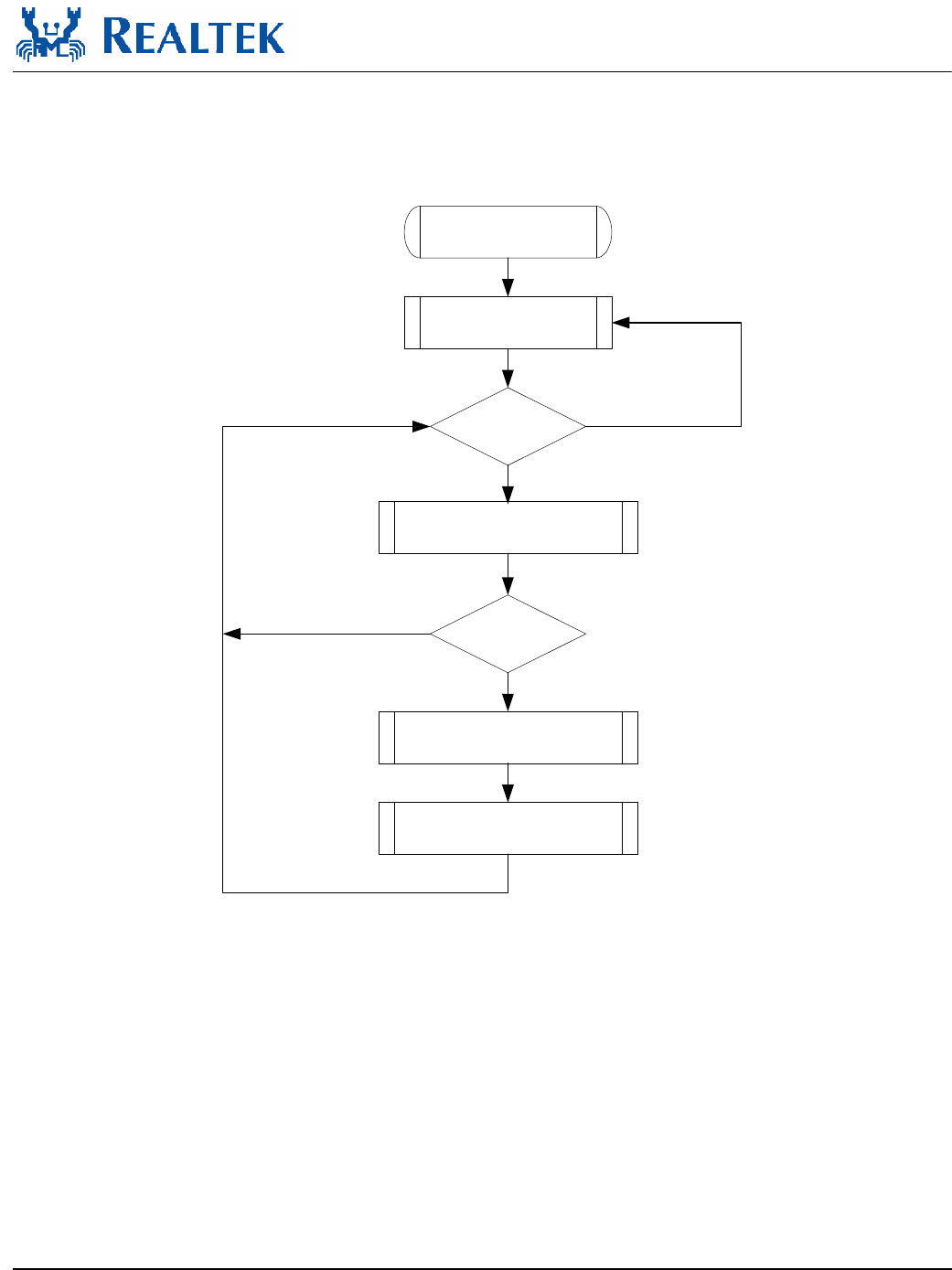
11.5.6. LINK/ACT LED
Blinking of the LINK/ACT LED indicates that the RTL8187L is linked and operating properly. If this LED
is high for extended periods it indicates that a link problem exists.
Power On
Link?
LED = High
LED = Low
LED = Low for (12 +- 2) ms
No
Yes
Tx/Rx packet?
Yes
No
LED = High for (100 +- 10) ms
Figure 6. LINK/ACT LED
RTL8187L
Datasheet
Wireless LAN Network Interface Controller 31 Track ID JATR-1076-21 Rev. 1.2
12. Application Diagram
RTL8187L
LED
Regulators
Main/Aux. Power Power 3.3V, 1.8V
Power 3.3V, 1.8V
External
ROM/RAM
D-
D+
40MHz
Clock
EEPROM Power 3.3V
SIEMAC
Base
Band
Power 3.3V, 1.8V
External
RF
Devices
Antenna
Figure 7. Application Diagram
RTL8187L
Datasheet
Wireless LAN Network Interface Controller 32 Track ID JATR-1076-21 Rev. 1.2
13. Electrical Characteristics
13.1.
Temperature Limit Ratings
Table 31. Temperature Limit Ratings
Parameter Minimum Maximum Units
Storage temperature -55 +125 °C
Operating temperature -10 70 °C
13.2.
DC Characteristics
Table 32. DC Characteristics
Symbol Parameter Conditions Minimum Typical Maximum Units
VDD33 3.3V Supply Voltage 3.0 3.3 3.6 V
VDD18 1.8V Supply Voltage 1.7 1.8 1.9 V
Voh Minimum High Level Output
Voltage
Ioh = -8mA 0.9 * Vcc Vcc V
Vol Maximum Low Level Output
Voltage
Iol = 8mA 0.1 * Vcc V
Vih Minimum High Level Input Voltage 0.5 * Vcc Vcc+0.5 V
Vil Maximum Low Level Input Voltage -0.5 0.3 * Vcc V
Iin Input Current Vin =Vcc or GND -1.0 1.0 µA
Ioz Tri-State Output Leakage Current Vout =Vcc or GND -10 10 µA
Icc Average Operating Supply Current Iout = 0mA, 460 mA
RTL8187L
Datasheet
Wireless LAN Network Interface Controller 33 Track ID JATR-1076-21 Rev. 1.2
13.3.
AC Characteristics
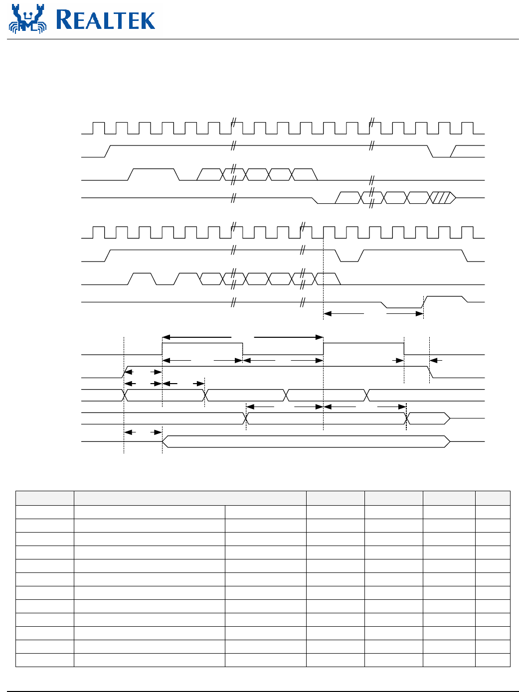
13.3.1. Serial EEPROM Interface Timing (93C46(64*16)/93C56(128*16))
EESK
EECS
EEDI
EEDO
110An A2 A0A1
Dn D1 D0
EESK
(Read)
(Write)
(Read)
(Write)
0
tcs
EESK
EECS
EEDI
EEDO
110AnA0
...
Dn
tcs
... D0
BUSY READY
High Impedance
High Impedance
twp
EECS
EEDI
EEDO
EEDO
(Read)
(Program) STATUS VALID
tsk
tskh tskl
tcss
tdis tdih
tdos tdoh
tcsh
tsv
Figure 8. Serial EEPROM Interface Timing
Table 33. EEPROM Access Timing Parameters
Symbol Parameter Minimum Typical Maximum Units
tcs Minimum CS Low Time 9346/9356 1000/250 ns
twp Write Cycle Time 9346/9356 10/10 ms
tsk SK Clock Cycle Time 9346/9356 4/1 µs
tskh SK High Time 9346/9356 1000/500 ns
tskl SK Low Time 9346/9356 1000/250 ns
tcss CS Setup Time 9346/9356 200/50 ns
tcsh CS Hold Time 9346/9356 0/0 ns
tdis DI Setup Time 9346/9356 400/50 ns
tdih DI Hold Time 9346/9356 400/100 ns
tdos DO Setup Time 9346/9356 2000/500 ns
tdoh DO Hold Time 9346/9356 2000/500 ns
tsv CS to Status Valid 9346/9356 1000/500 ns
RTL8187L
Datasheet
Wireless LAN Network Interface Controller 34 Track ID JATR-1076-21 Rev. 1.2
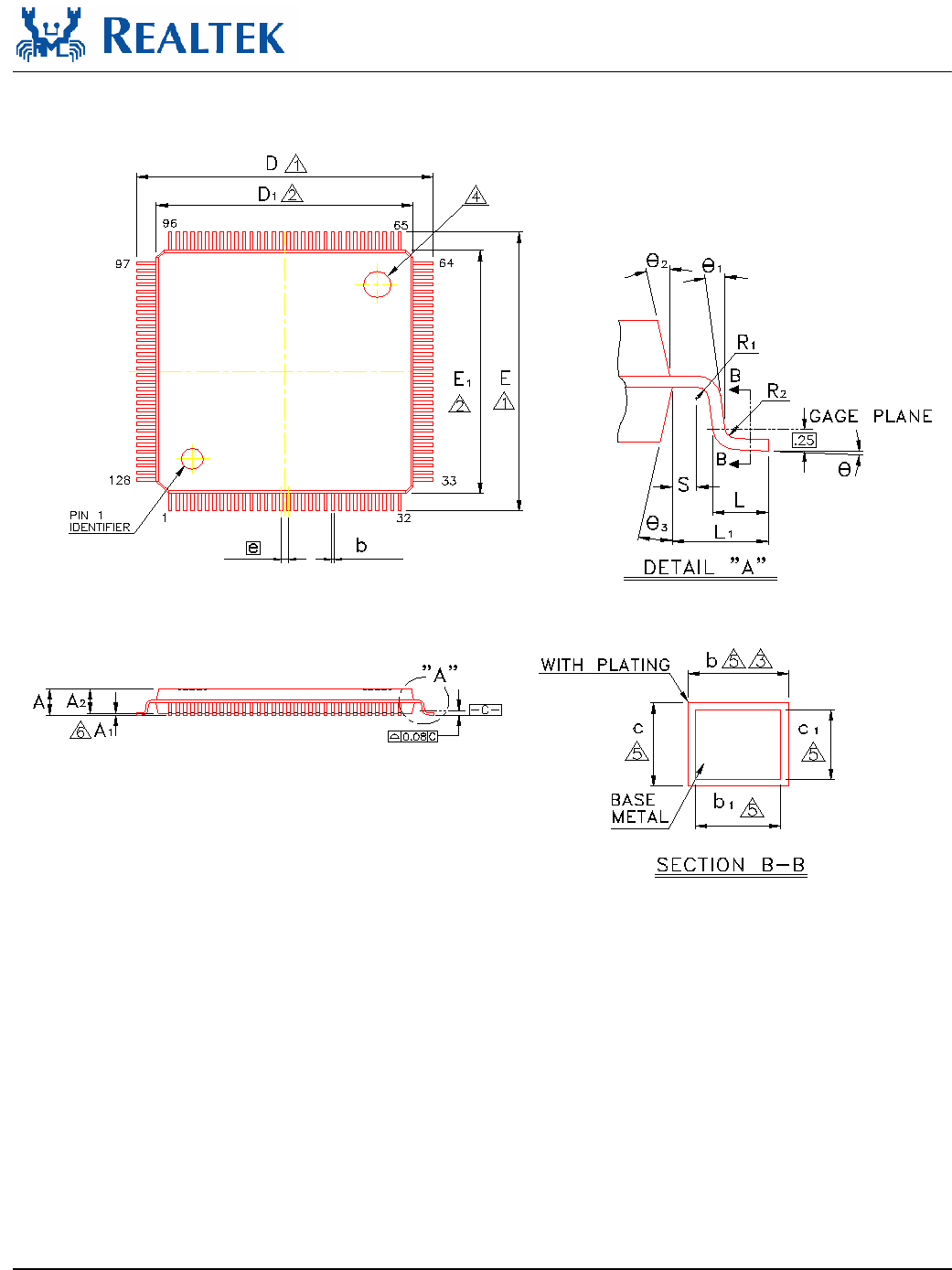
14. Mechanical Dimensions
See the Mechanical Dimensions notes on the next page.
RTL8187L
Datasheet
Wireless LAN Network Interface Controller 35 Track ID JATR-1076-21 Rev. 1.2
14.1.
Mechanical Dimensions Notes
Note:
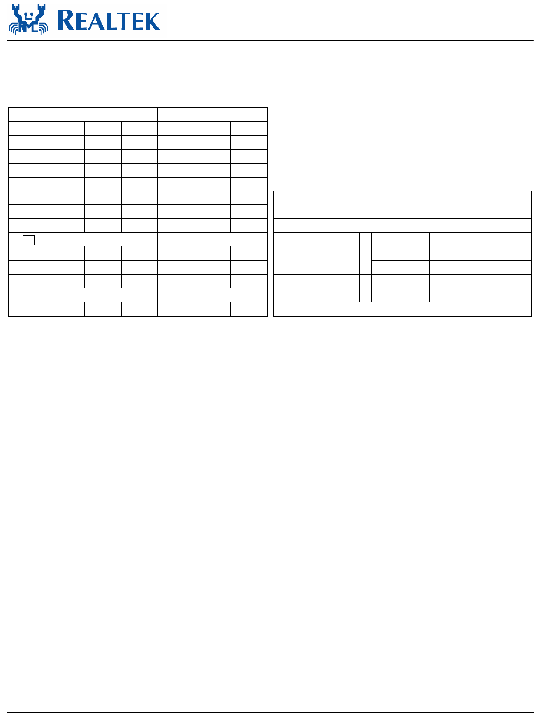
Symbol Dimension in inch Dimension in mm 1.Dimension b does not include dambar
Min Typical Max Min Typical Max
protrusion/intrusion.
A - - 0.063 - - 1.60
2.Controlling dimension: Millimeter
A1 0.002 - - 0.05 - -
3.General appearance spec. should be based
A2 0.053 0.055 0.057 1.35 1.40 1.45 on final visual inspection spec.
b 0.005 0.007 0.009 0.13 0.18 0.23
c 0.004 - 0.006 0.09 - 0.20
TITLE: 128LD LQFP ( 14x14x1.4 mm*2 ) PACKAGE OUTLINE
D 0.624 0.630 0.636 15.85 16.00 16.15 -CU L/F, FOOTPRINT 2.0 mm
D1 0.547 0.551 0.555 13.90 14.00 14.10 LEADFRAME MATERIAL:
e 0.016 BSC 0.40 BSC APPROVE DOC. NO. 530-ASS-P004
E 0.624 0.630 0.636 15.85 16.00 16.15 VERSION 1
E1 0.547 0.551 0.555 13.90 14.00 14.10 PAGE OF
L 0.018 0.024 0.030 0.45 0.60 0.75 CHECK DWG NO. LQ128 - 2
L1 0.039 REF 1.00 REF DATE MAY. 13.2002
Θ 0° 3.5° 7° 0° 3.5° 7°
REALTEK SEMICONDUCTOR CORP.

RTL8187L
Datasheet
Wireless LAN Network Interface Controller 36 Track ID JATR-1076-21 Rev. 1.2
15. Ordering Information
Table 34. Ordering Information
Part Number Package Status
RTL8187L 128-pin LQFP MP
RTL8187L-LF RTL8187L with Lead (Pb)-Free package MP
Realtek Semiconductor Corp.
Headquarters
No. 2, Industry East Road IX, Science-based
Industrial Park, Hsinchu, 300, Taiwan, R.O.C.
Tel: 886-3-5780211 Fax: 886-3-5776047
www.realtek.com.tw
Federal Communication Commission Interference Statement
This equipment has been tested and found to comply with the limits for a Class B digital
device, pursuant to Part 15 of the FCC Rules. These limits are designed to provide
reasonable protection against harmful interference in a residential installation. This
equipment generates, uses and can radiate radio frequency energy and, if not installed and
used in accordance with the instructions, may cause harmful interference to radio
communications. However, there is no guarantee that interference will not occur in a
particular installation. If this equipment does cause harmful interference to radio or
television reception, which can be determined by turning the equipment off and on, the
user is encouraged to try to correct the interference by one of the following measures:
Reorient or relocate the receiving antenna.
Increase the separation between the equipment and receiver.
Connect the equipment into an outlet on a circuit different from that to which the
receiver is connected.
Consult the dealer or an experienced radio/TV technician for help.
FCC Caution: Any changes or modifications not expressly approved by the party
responsible for compliance could void the user's authority to operate this equipment.
This device complies with Part 15 of the FCC Rules. Operation is subject to the following
two conditions: (1) This device may not cause harmful interference, and (2) this device
must accept any interference received, including interference that may cause undesired
operation.
This device and its antenna(s) must not be co-located or operating in conjunction with
any other antenna or transmitter.
This device is intended only for OEM integrators under the following conditions:
OEM integrator is still responsible for testing their end product for any additional
compliance requirements required with this module installed (for example, digital device
emissions, PC peripheral requirements, etc.).
IMPORTANT NOTE: In the event that these conditions can not be met (for example
certain laptop configurations or co-location with another transmitter), then the FCC
authorization is no longer considered valid and the FCC ID can not be used on the final
product. In these circumstances, the OEM integrator will be responsible for re-evaluating
the end product (including the transmitter) and obtaining a separate FCC authorization.
Without Co-located
The antenna (s) used for this transmitter must not be co-located or operating in
conjunction with any other antenna or transmitter.
Modular Approval
OEM integrator is still responsible for testing their end product for any additional
compliance requirements required with this module installed (for example, digital device
emissions, PC peripheral requirements, etc.).
IMPORTANT NOTE: In the event that these conditions can not be met (for example
certain laptop configurations or co-location with another transmitter), then the FCC
authorization is no longer considered valid and the FCC ID can not be used on the final
product. In these circumstances, the OEM integrator will be responsible for re-evaluating
the end product (including the transmitter) and obtaining a separate FCC authorization.
Modular OEM Integrator Notice
End Product Labeling
This transmitter module is authorized only for use in device where the antenna may be
installed such that 20 cm may be maintained between the antenna and users. The final
end product must be labeled in a visible area with the following: “Contains TX FCC ID:
TX2-RTL8187”.
IC Radiation Exposure Statement:
"Operation is subject to the following two conditions: (1) this device may not cause
interference, and (2) this device must accept any interference, including interference that
may cause undesired operation of the device."
OEM integrator is still responsible for testing their end product for any additional
compliance requirements required with this module installed (for example, digital device
emissions, PC peripheral requirements, etc.).
IMPORTANT NOTE: In the event that these conditions can not be met (for example
certain laptop configurations or co-location with another transmitter), then the FCC
authorization is no longer considered valid and the FCC ID can not be used on the final
product. In these circumstances, the OEM integrator will be responsible for re-evaluating
the end product (including the transmitter) and obtaining a separate FCC authorization.
This transmitter module is authorized only for use in device where the antenna may be
installed such that 20 cm may be maintained between the antenna and users. The final
end product must be labeled in a visible area with the following: “Contains TX IC ID:
6317A–RTL8187”.

This device has been designed to operate with an antenna having a maximum gain of
[3.00] dBi. Antenna having a higher gain is strictly prohibited per regulations of
Industry Canada. The required antenna impedance is 50 ohms."
List of antennas below:
Ant. Type PIFA PK
Gain(dBi) 3 Ant. Type PIFA PK
Gain(dBi) 2.32
1. Connector IPEX Model
No. DQ661500301 2. Connector IPEX Model No. MA6001
Ant. Type PIFA PK
Gain(dBi) 2.39 Ant. Type PIFA PK
Gain(dBi) 2.11
3. Connector IPEX Model
No. AR830WIPI02A 4. Connector IPEX Model No. AR320WIPI02B
Ant. Type PIFA PK
Gain(dBi) 0.78 Ant. Type PIFA PK
Gain(dBi) 1.1
5. Connector IPEX Model
No. WDAN-QMA6002
-DF
6. Connector IPEX Model No. DQ661500115
Ant. Type PIFA PK
Gain(dBi) 0.3 Ant. Type PIFA PK
Gain(dBi) 2.57
7. Connector IPEX Model
No. AAFJ5050002LF0 8. Connector IPEX Model No. AR620WIPI02C
Ant. Type PIFA PK
Gain(dBi) 1.97 Ant. Type PIFA PK
Gain(dBi) 1
9. Connector IPEX Model
No. ARMK8WIPI02A
10
. Connector IPEX Model No. ARMK8WIPI02A
Ant. Type PIFA PK
Gain(dBi) 2.37 Ant. Type PIFA PK
Gain(dBi) 2.11
11
. Connector IPEX Model
No. AAFA5050004LQ
0
12
. Connector IPEX Model No. AR320WIPI01B
Ant. Type PIFA PK
Gain(dBi) 2.57 Ant. Type PIFA PK
Gain(dBi) 2.21
13
. Connector IPEX Model
No. B0785028000003
14
. Connector IPEX Model No. AR330WIPI01D
Ant. Type PIFA PK
Gain(dBi) 2.55 Ant. Type PIFA PK
Gain(dBi) 2.48
15
. Connector IPEX Model
No. AR621WIPI02D
16
. Connector IPEX Model No. ARW62WIPI01G
Ant. Type PIFA PK
Gain(dBi) 2.49 Ant. Type PIFA PK
Gain(dBi) 0.46
17
. Connector IPEX Model
No. ARK8MWIPI01B
18
. Connector IPEX Model No. AAFQ5050001L
K0
Ant. Type PIFA PK
Gain(dBi) 2.86 Ant. Type PIFA PK
Gain(dBi) 2.45
19
. Connector IPEX Model
No. AAFQ5050002LK
0
20
. Connector IPEX Model No. B012502800000
4
Ant. Type PIFA PK
Gain(dBi) 0.74 Ant. Type PIFA PK
Gain(dBi) 0.03
21
. Connector IPEX Model
No. MA6002
22
. Connector IPEX Model No. W340UA1
To reduce potential radio interference to other users, the antenna type and its gain
should be so chosen that the equivalent isotropically radiated power (e.i.r.p.) is not
more than that permitted for successful communication.

Installation
Guide__
Installation Guide__
R
Re
ea
al
lt
te
ek
k
R
RT
TL
L8
81
18
87
7
+
+
R
RT
TL
L8
82
22
25
5-
-V
VF
F
(
(Z
Z2
2)
)
8
80
02
2.
.1
11
1
b
b/
/g
g
m
mi
in
ni
iC
Ca
ar
rd
d
Date: 2006/06/06
Version: 1.0
This document is subject to change without notice. The document
contains Realtek confidential information and must not be disclosed
to any third party without appropriate NDA.
Installation Description
This module is to be installed only by the professionals.
When IRF303JU/IRF303U2is installed in a product, we shall consider the following points;
1. Since RTL8187 miniCard owns its FCC ID Number/IC Number, we shall affix an exterior
label on the outside of the product if the FCC ID/IC Number is not visible. The exterior label
shall use wording such as either “Contains Transmitter Module FCC ID: TX2-RTL8187/IC
Number: 6317A-RTL8187”or “Contains FCC ID: TX2-RTL8187/ IC Number: 6317A-RTL8187”.
2. RTL8187 miniCard complies with requirements of sub-sections 15.203, 15.205, 15.207,
15.247 and 15.407 in FCC Rules Part 15. We shall installRTL8187 miniCard in accordance
with their requirements. RTL8187 miniCard complies with requirements of the sub-section
2.1091. When installers install RTL8187 miniCard into a product, they shall ensure that the
public is not exposedto radio frequency energy levels in excess of the Commission’s
guidelines in accordance with the sub-section 15.247(e)(i) and 15.407(f) in FCC Rules Part 15.