Realtek Semiconductor RTL8187B 802.11b/g RTL8187B miniCard User Manual Realtek RTL8187B DataSheet 1 0
Realtek Semiconductor Corp. 802.11b/g RTL8187B miniCard Realtek RTL8187B DataSheet 1 0
UserManual.wiki
>
Realtek Semiconductor
>
RTL8187B User Manual
Users Manual
Navigation menu
Upload a User Manual
Namespaces
Wiki Guide
HTML
PDF
Info
Views
User Manual
Discussion / Help
Navigation
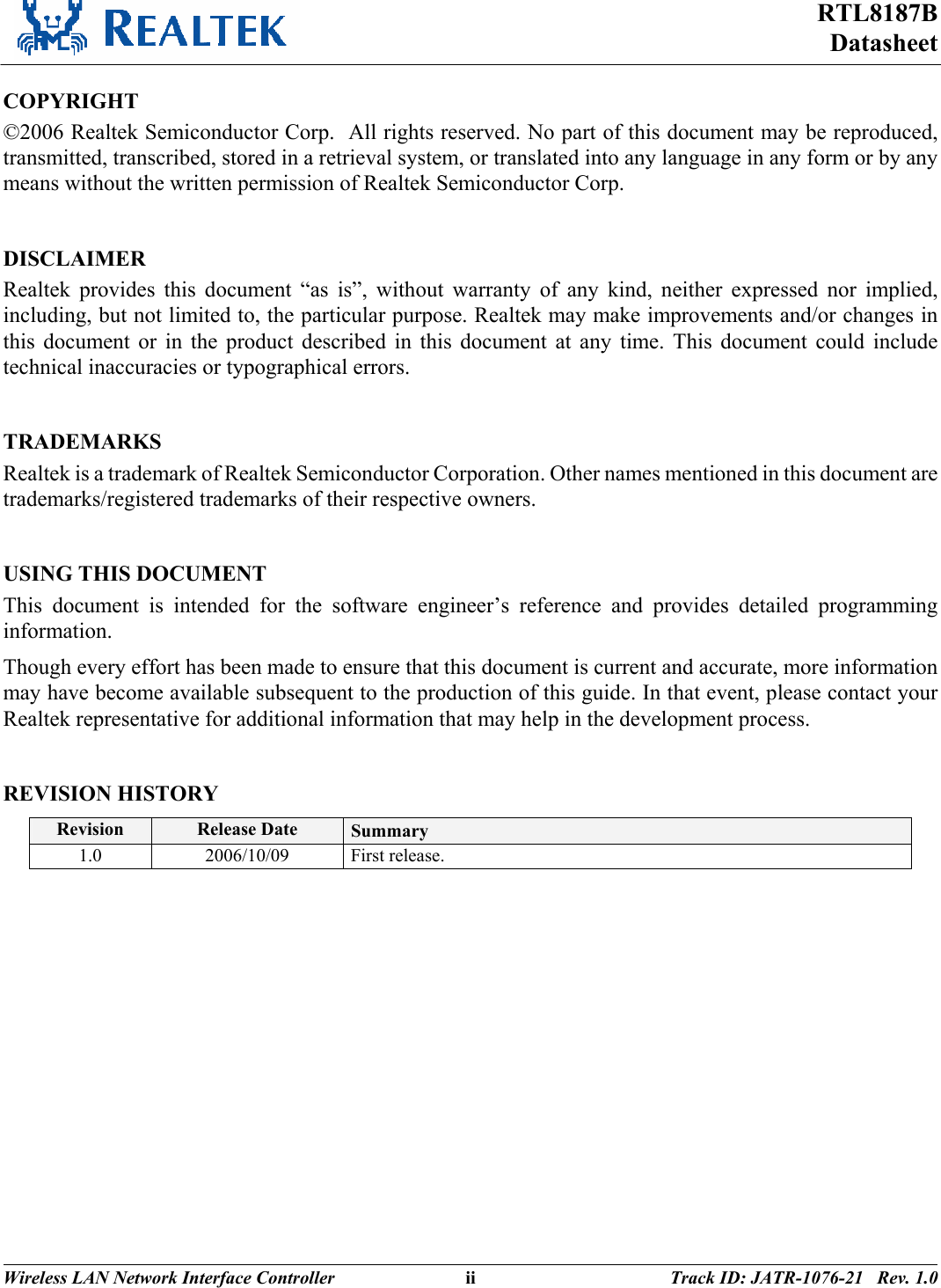
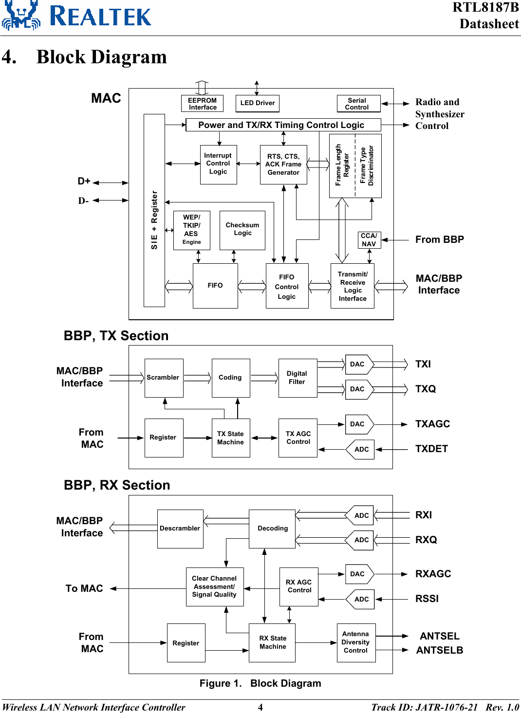
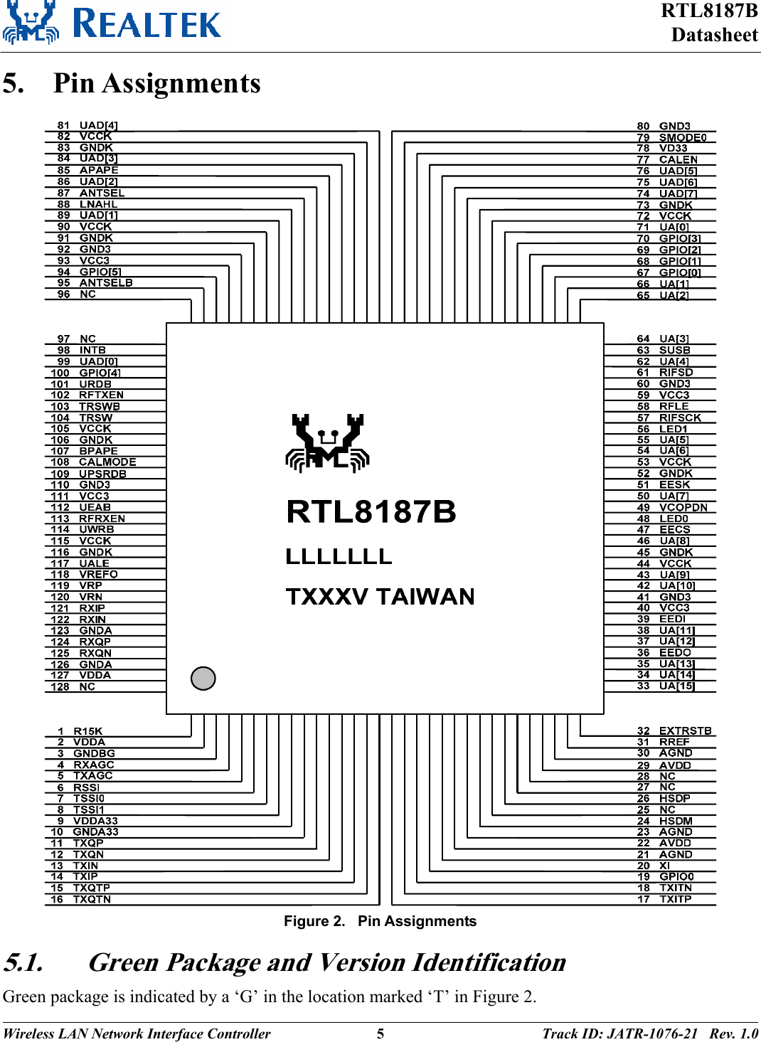
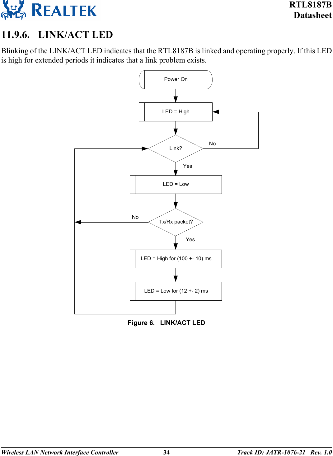
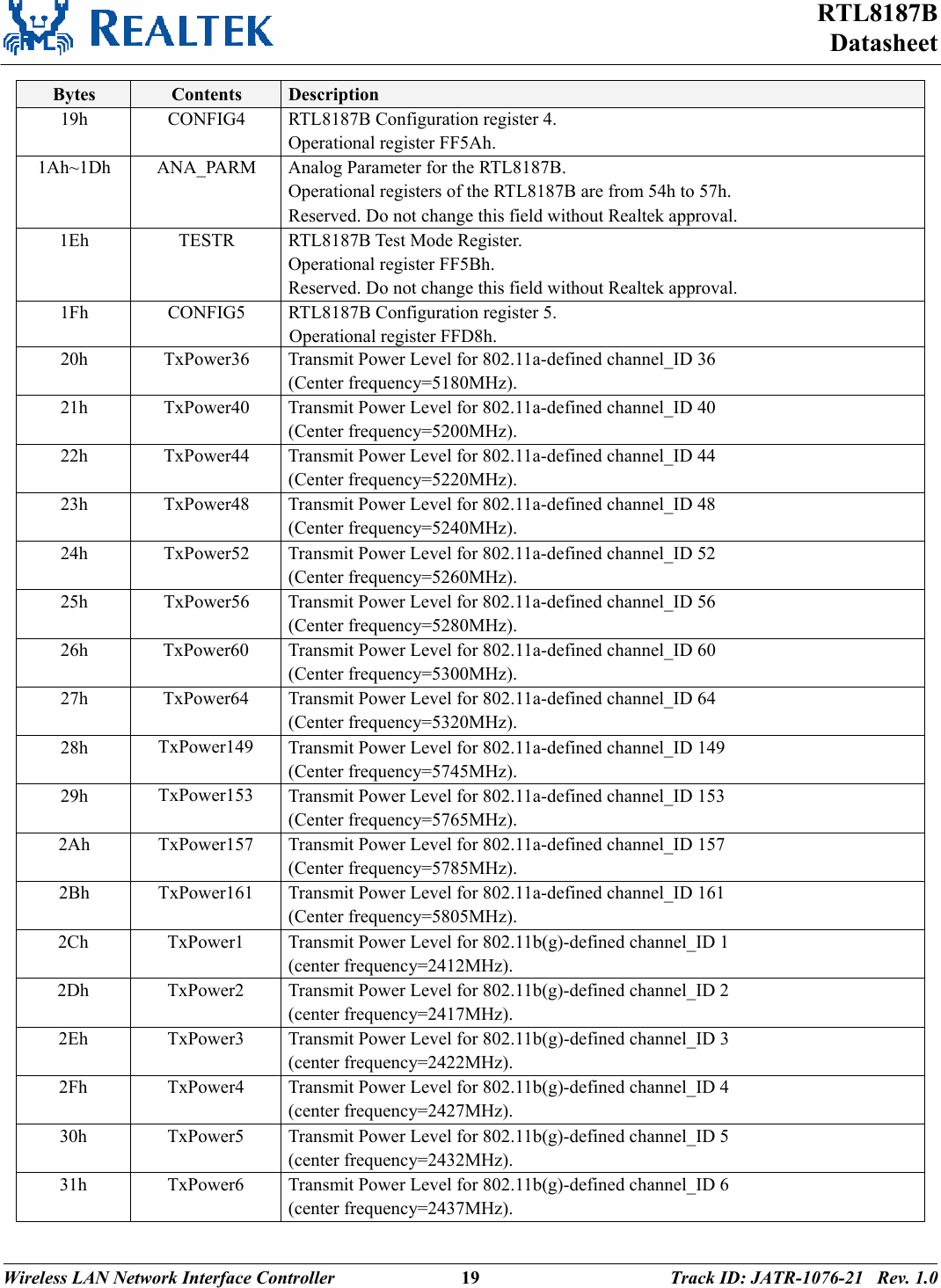
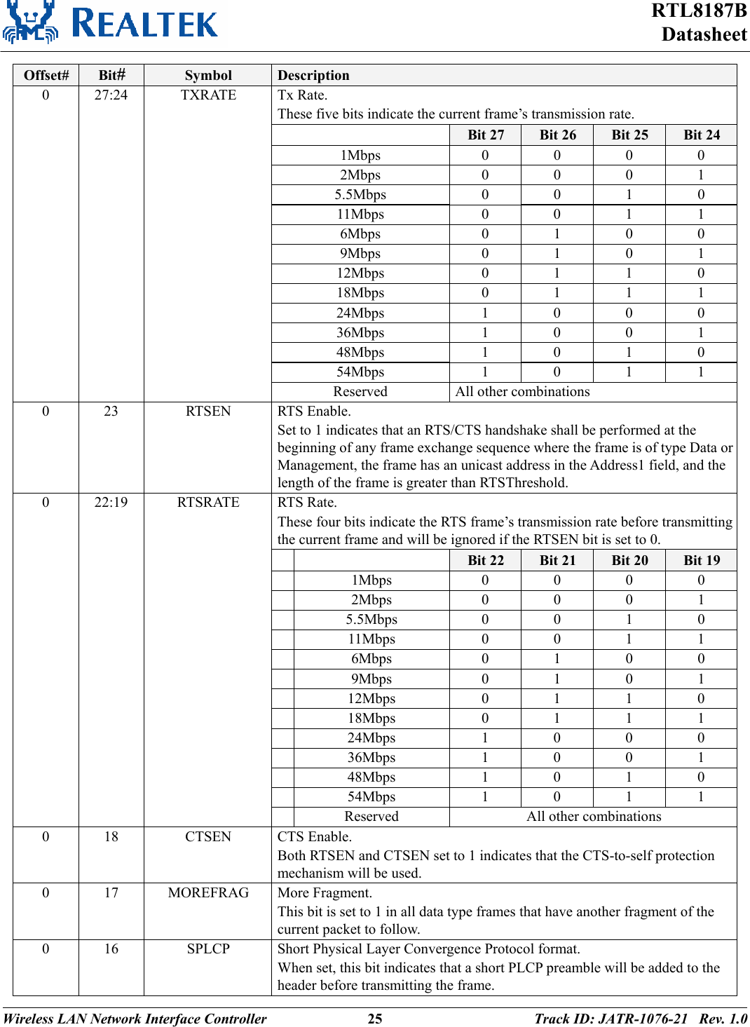
![RTL8187B Datasheet Wireless LAN Network Interface Controller 9 Track ID: JATR-1076-21 Rev. 1.0 Symbol Type Pin No Description RFTXEN O 102 Not used in the RTL8255 RF chipset. RFRXEN O 113 Not used in the RTL8255 RF chipset. GPIO[0] O 67 General purpose input/output pin. GPIO[1] O 68 General purpose input/output pin. GPIO[2] O 69 General purpose input/output pin. GPIO[3] O 70 General purpose input/output pin. GPIO[4] O 100 General purpose input/output pin. GPIO[5] O 94 General purpose input/output pin. VREFO X 118 Not used in the RTL8255 RF chipset. VRP X 119 Not used in the RTL8255 RF chipset. VRN X 120 Not used in the RTL8255 RF chipset. RXIP RXIN I I 121 122 Receive (Rx) In-phase Analog Data. RXQP RXQN I I 124 125 Receive (Rx) Quadrature-phase Analog Data. RXAGC O 4 Not used in the RTL8255 RF chipset. TXAGC O 5 Not used in the RTL8255 RF chipset. RSSI I 6 Analog Input to the Receive Power A/D Converter for Receive AGC Control. TSSI0 I 7 Input to the Transmit Power A/D Converter for 2.4GHz Transmit AGC Control. TSSI1 I 8 Input to the Transmit Power A/D Converter for 5GHz Transmit AGC Control. TXQP TXQN O O 11 12 Transmit (TX) Quadrature-phase Analog Data. TXIP TXIN O O 14 13 Transmit (TX) In-phase Analog Data. TXQTP TXQTN O O 15 16 Not used in the RTL8255 RF chipset. TXITP TXITN O O 17 18 Not used in the RTL8255 RF chipset. 6.6. Clock and Other Pins Table 7. Clock and Other Pins Symbol Type Pin No Description R15K I/O 1 This pin must be pulled low by a 15K Ω resistor. XI I 20 40MHz clock Input. EXTRSTB I 32 Pull high 3.3V. If pulled low, the whole chip will be reset.](https://usermanual.wiki/Realtek-Semiconductor/RTL8187B/User-Guide-755798-Page-14.png)
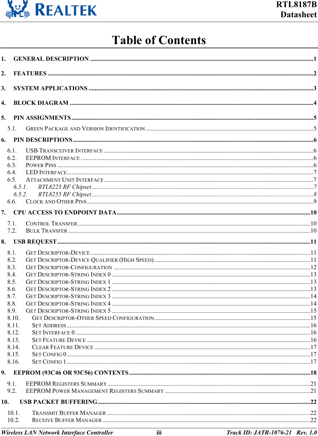
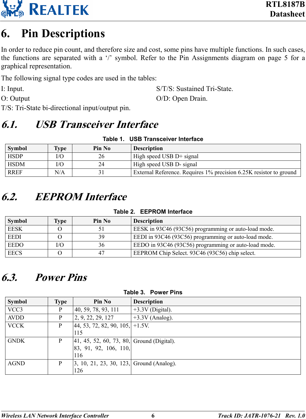
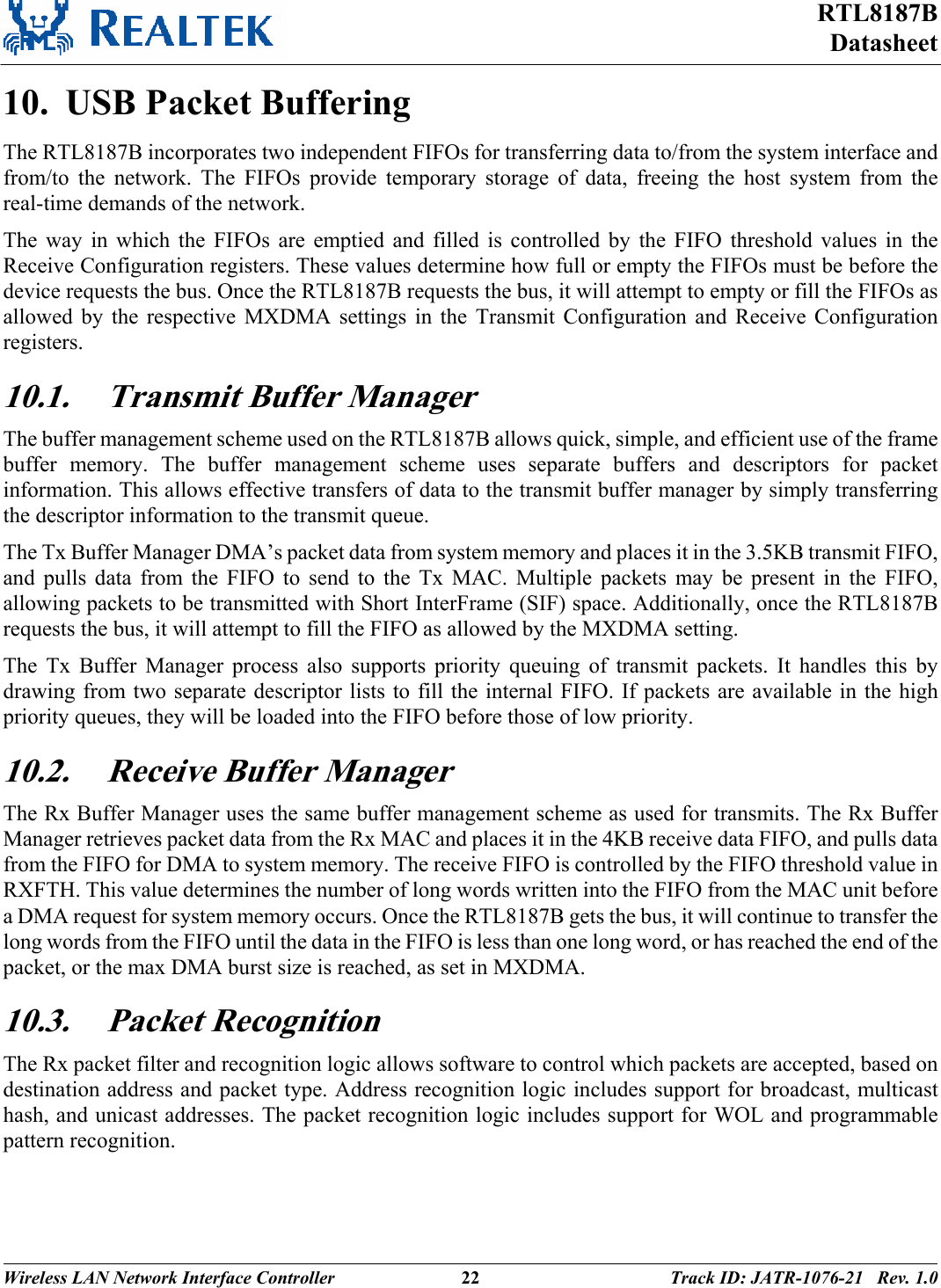
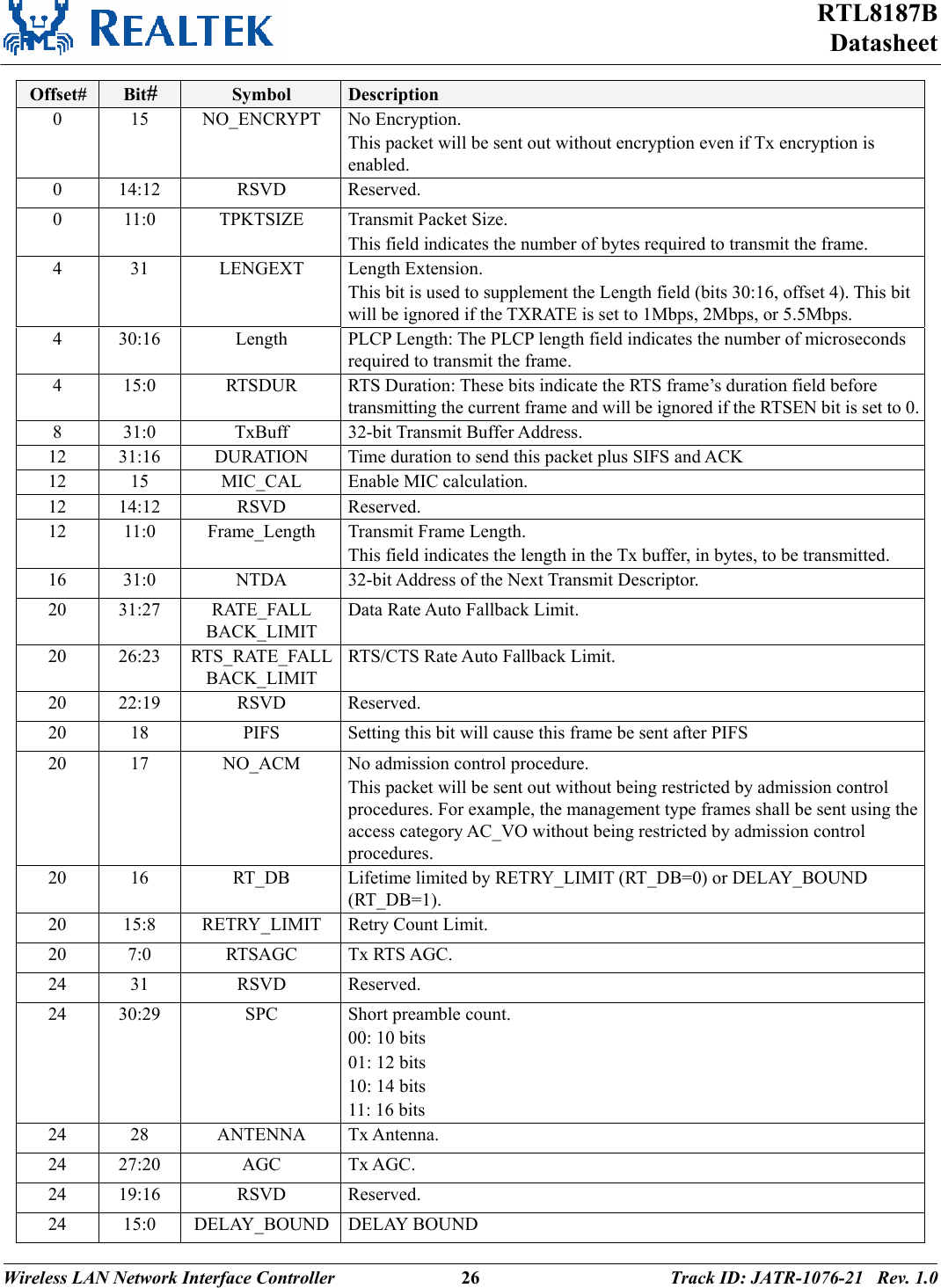
![RTL8187B Datasheet Wireless LAN Network Interface Controller 18 Track ID: JATR-1076-21 Rev. 1.0 9. EEPROM (93C46 or 93C56) Contents The RTL8187B supports the attachment of an external EEPROM. The 93C46 is a 1Kbit EEPROM (the 93C56 is a 2Kbit EEPROM). The EEPROM interface provides the ability for the RTL8187B to read from, and write data to, an external serial EEPROM device. If the EEPROM is not present, the RTL8187B initialization uses default values for the Operational Registers. Software can read and write to the EEPROM using “bit-bang” accesses via the 9346CR Register. Although it is actually addressed by words, its contents are listed below by bytes for convenience. After the initial power on or auto-load command in the 9346CR, the RTL8187B performs a series of EEPROM read operations from the 93C46 (93C56). Note: It is suggested to obtain Realtek approval before changing the default settings of the EEPROM. Table 24. EEPROM (93C46 or 93C56) Contents Bytes Contents Description 00h 29h 01h 81h These 2 bytes contain the ID code word for the RTL8187B. The RTL8187B will load the contents of the EEPROM into the corresponding location if the ID word (8129h) is correct. 02h-03h VID USB Vendor ID. 04h-05h DID USB Device ID. 06h ChannelPlan Channel Plan: Map of channels to be scanned. 07h Reserved - 08h Reserved - 09h Version Bit [7:6] Interface Selection 00 : USB 01 : Mini Card 02 : Reserved 03 : Reserved Bit [5:0] The EEPROM version. 0Ah Tx Power Base Tx power of the serving base station. 0Bh Reserved - 0Ch RFChipID RF Chip ID. The identifier of the RF chip. 0Dh CONFIG3 RTL8187B Configuration register 3. Operational register FF59h. 0Eh~13h MAC Address MAC Address. After the auto-load command or a hardware reset, the RTL8187B loads MAC Addresses to IDR0~IDR5 of the I/O registers of the RTL8187B. 14h TxPower12 Transmit Power Level for 802.11b(g)-defined channel_ID 12 (center frequency=2467MHz). 15h CONFIG1 RTL8187B Configuration register 1. Operational register FF52h. Bit[5:2] : USB receive sensitivity 16h~17h CRC 16-bit CRC value of EEPROM content. Reserved for Software use. 18h CONFIG2 RTL8187B Configuration register 2. Operational register FF53h.](https://usermanual.wiki/Realtek-Semiconductor/RTL8187B/User-Guide-755798-Page-23.png)
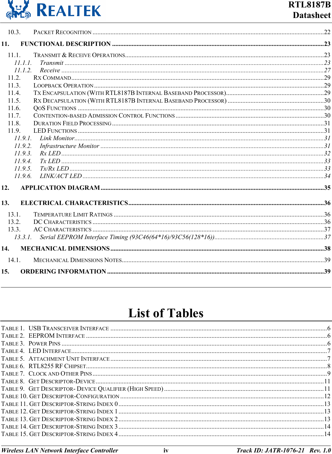
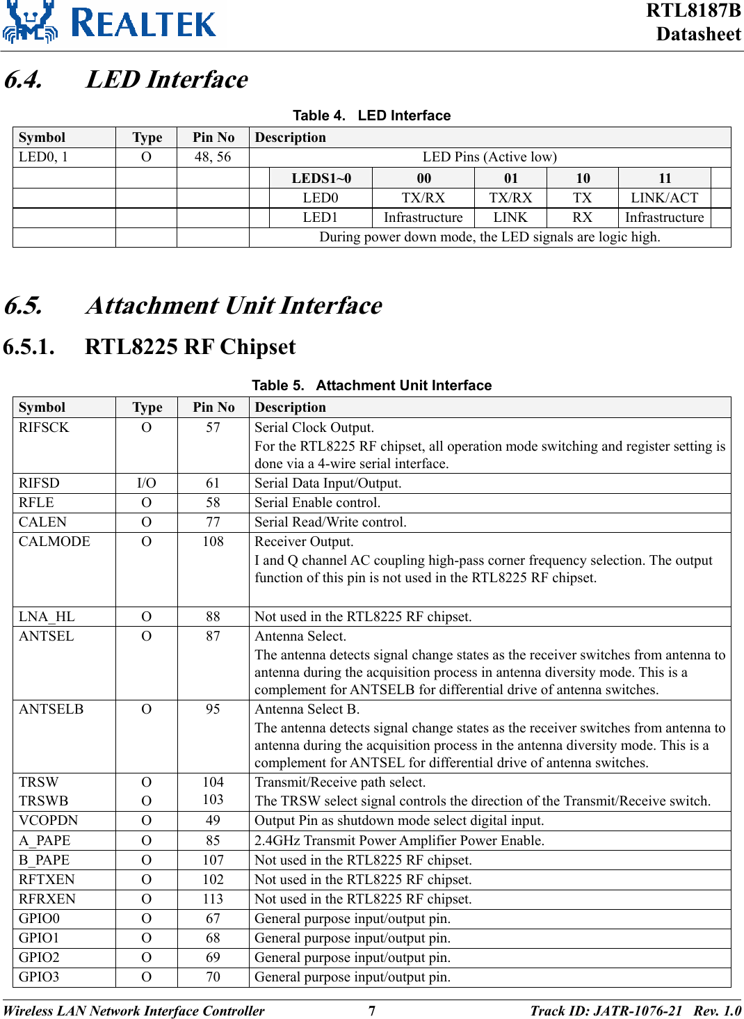
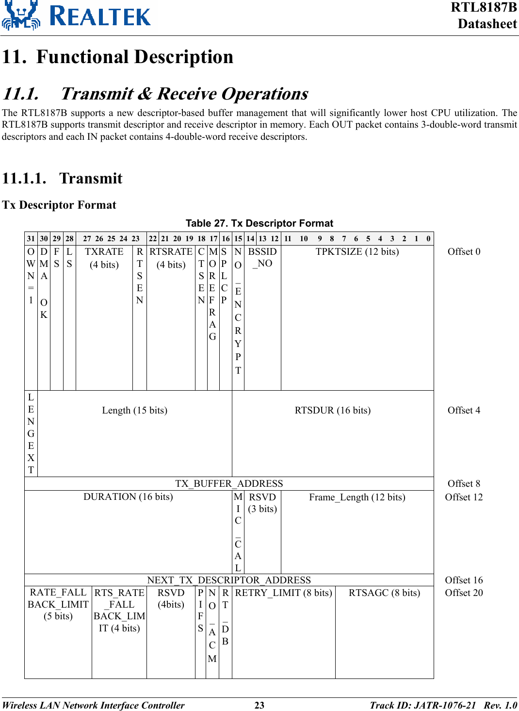
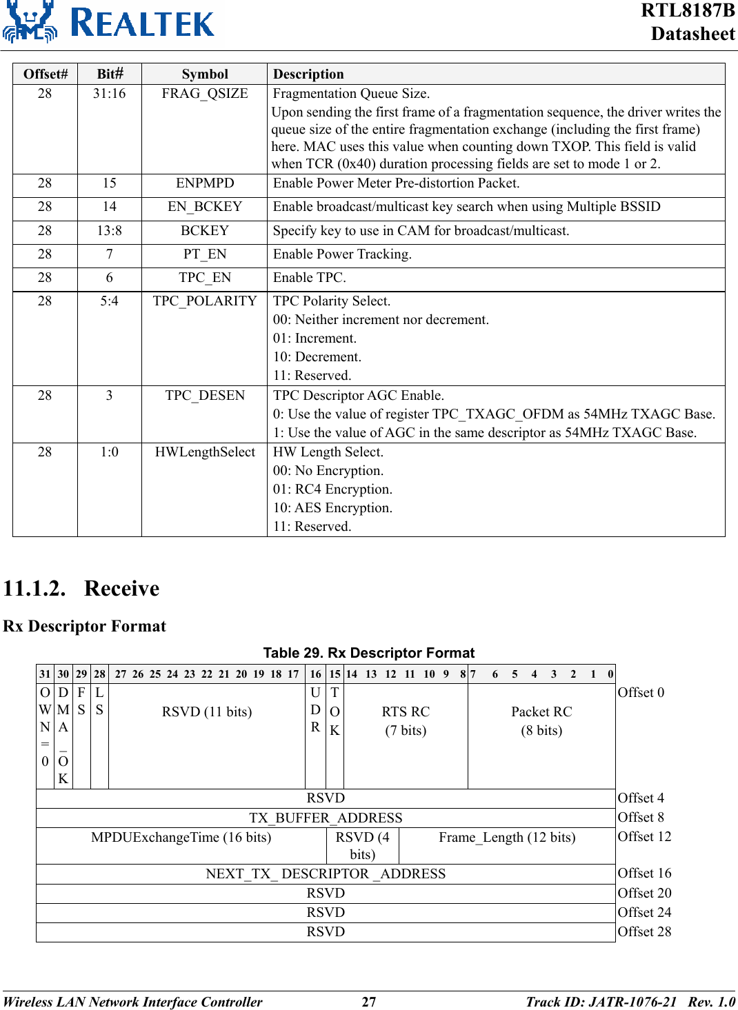
![RTL8187B Datasheet Wireless LAN Network Interface Controller 20 Track ID: JATR-1076-21 Rev. 1.0 Bytes Contents Description 32h-35h ANA_PARM2 Analog Parameter 2 for RTL8187B. Operational registers for the RTL8187B are 60h to 63h. Reserved. Do not change this field without Realtek approval. 36h TxPower11 Transmit Power Level for 802.11b(g)-defined channel_ID 11 (center frequency=2462MHz). 37h Optional functions Bit[1:0]: Suspend pin behavior. 00b: Default pull high 01b: Default pill low 10b: Functions as a PME# signal Bit[2]: USB remote wake up function. 0: No remote wake up feature for RTL8187B 1: Remote wake up feature for RTL8187B Bit[3] : UART Support. 0: No UART interface support 1: UART interface support Bit[5:4]: Response default serial number. 00b: Respond serial number from EEPROM 01b: Respond serial number from internal ROM, 00 E0 4C 00 00 01 Others : Reserved Bit[6] : Device Power. 0: Bus power 1: Self power 38h TxPower13 Transmit Power Level for 802.11b(g)-defined channel_ID 13 (center frequency=2472MHz). 39h TxPower14 Transmit Power Level for 802.11b(g)-defined channel_ID 14 (center frequency=2484MHz). 3Ah-73h Manufacture String & Product String Manufacture String and Product String:Those bits specify both manufacturer’s information and device’s information for the USB standard request. Maximum two strings total length are 58 bytes. 74h-79h - Reserved. 7Ah TxPower7 Transmit Power Level for 802.11b(g)-defined channel_ID 7 (center frequency=2442MHz). 7Bh TxPower8 Transmit Power Level for 802.11b(g)-defined channel_ID 8 (center frequency=2447MHz). 7Ch TxPower9 Transmit Power Level for 802.11b(g)-defined channel_ID 9 (center frequency=2452MHz). 7Dh TxPower10 Transmit Power Level for 802.11b(g)-defined channel_ID 10 (center frequency=2457MHz). 7Eh CustomerID BIT[0-7]: CustomerID, 0x00 and 0xFF is reserved for Realtek. 7Fh SW Antenna Diversity BIT[0:1]: 01b enables SW Antenna Diversity. BIT[2:3]: 01b is default antenna.](https://usermanual.wiki/Realtek-Semiconductor/RTL8187B/User-Guide-755798-Page-25.png)
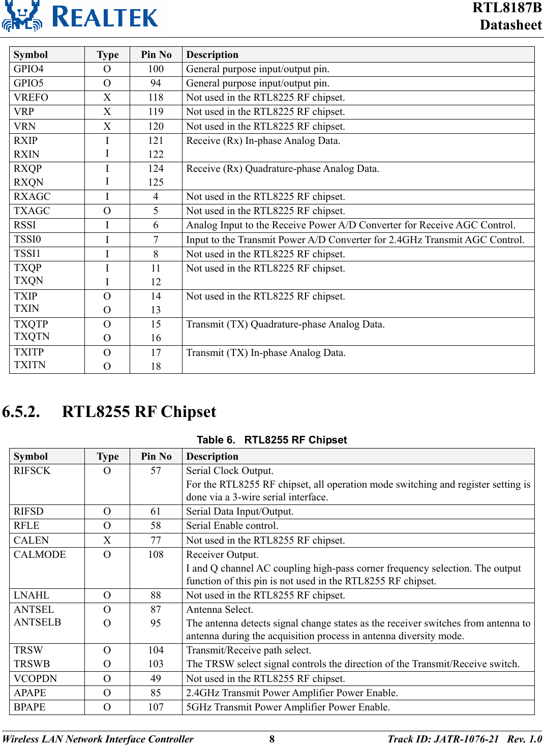
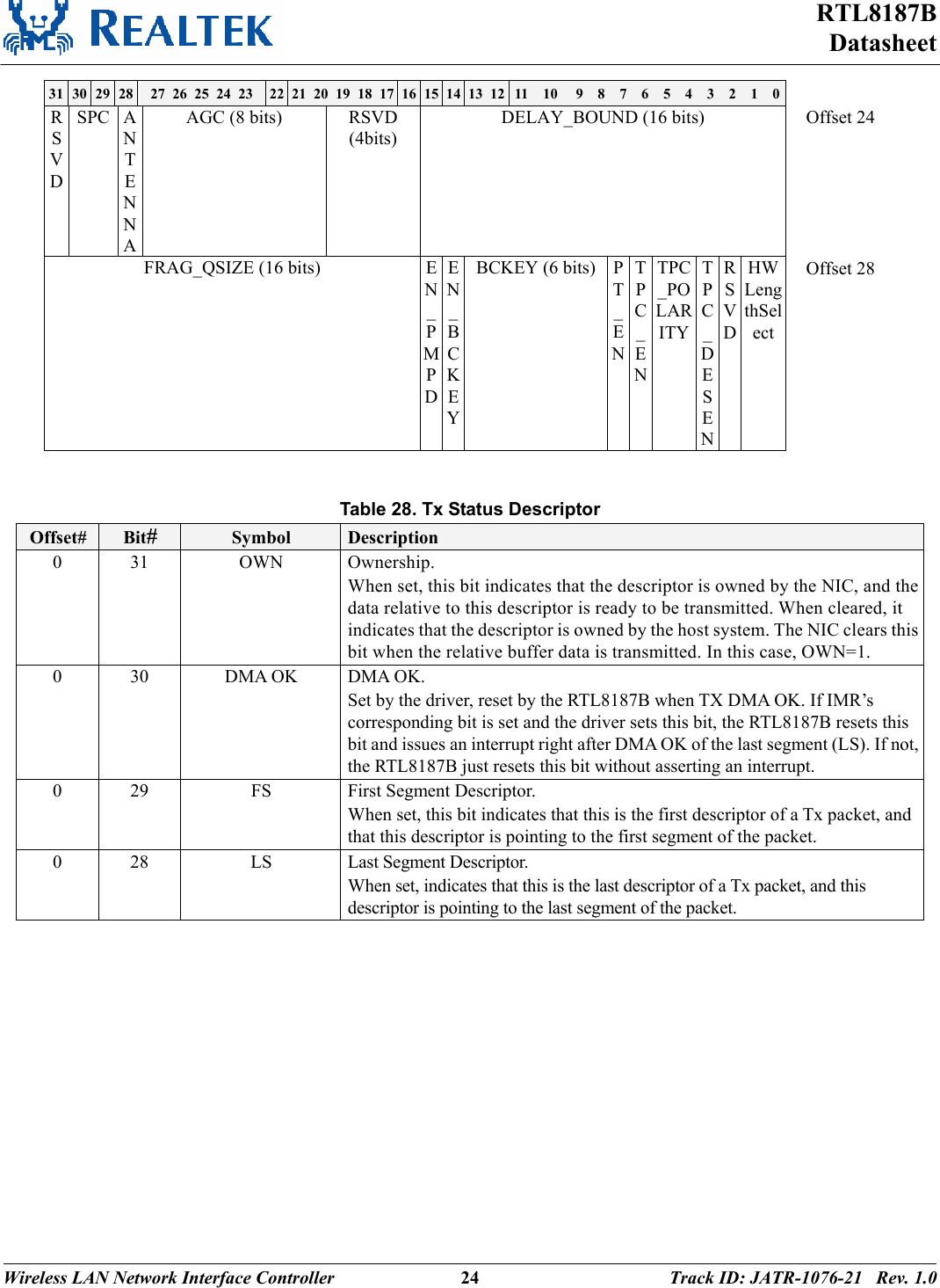
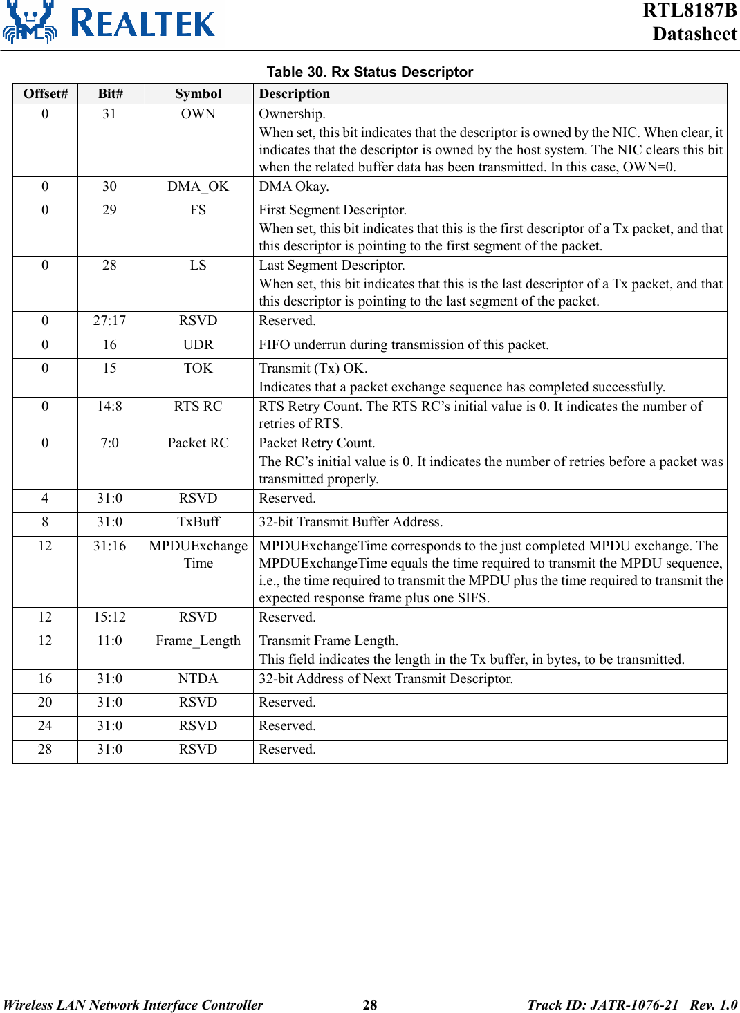
![RTL8187B Datasheet Wireless LAN Network Interface Controller 21 Track ID: JATR-1076-21 Rev. 1.0 9.1. EEPROM Registers Summary Table 25. EEPROM Registers Summary Address Name Type Bit7 Bit6 Bit5 Bit4 Bit3 Bit2 Bit1 Bit0 FF00h- FF05h IDR0 – IDR5 R/W* R LEDS1 LEDS0 USB Receive Sensitivity - - FF52h CONFIG1 W* LEDS1 LEDS0 USB Receive Sensitivity - - R LCK - - - - PAPE _sign PAPE _time FF53h CONFIG2 W* - - - - - PAPE _sign PAPE _time FF54h- FF57h ANA_PARM R/W** 32-bit Read Write R - PARM_En Magic - - - - - FF59h CONFIG3 W* - PARM_En Magic - - - - - R - - - LWPME - LWPTN - FF5Ah CONFIG4 W* - - - LWPME - LWPTN - FF5Bh TESTR 8-bit Read Write FF60h- FF63h ANA_PARM2 R/W 32-bit Read Write FFD8h CONFIG5 R/W** - - - - - - LANWake - Note 1: Registers marked 'W*' can be written only if bits EEM1=EEM0=1. Note 2: Registers marked 'W**' can be written only if bits EEM1:0=[1:1] and CONFIG3<PARM_EN>= 0. 9.2. EEPROM Power Management Registers Summary Table 26. EEPROM Power Management Registers Summary Configuration Space Offset Name Type Bit7 Bit6 Bit5 Bit4 Bit3 Bit2 Bit1 Bit0 52h R Aux_I_b1 Aux_I_b0 DSI Reserved PMECLK Version 53h PMC R PME_D3cold PME_D3hot PME_D2 PME_D1 PME_D0 D2 D1 Aux_I_b2](https://usermanual.wiki/Realtek-Semiconductor/RTL8187B/User-Guide-755798-Page-26.png)
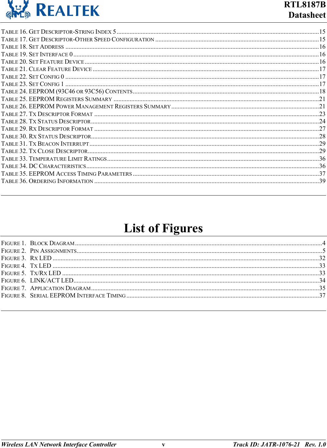
![RTL8187B Datasheet Wireless LAN Network Interface Controller 29 Track ID: JATR-1076-21 Rev. 1.0 11.2. Rx Command The RTL8187B supports an Rx command queue to feedback the Tx state and beacon interrupt . When the Command Type (bit[31:30]) is set to 00b, it indicates Tx Beacon Interrupt. When set to 01b, it indicates Tx Close Descriptor. Table 31. Tx Beacon Interrupt 31 30 29 28 27 26 25 24 23 22 21 20 19 18 17 16 15 14 13 12 11 10 9 8 7 6 5 4 3 2 1 0 Cmd Type RSVD Last Beacon CW Last Beacon TSF[31:0] Table 32. Tx Close Descriptor 31 30 29 28 27 26 25 24 23 22 21 20 19 18 17 16 15 14 13 12 11 10 9 8 7 6 5 4 3 2 1 0 Cmd Type FS LS Sequence No[11:0] TOKRTS Retry Count[6:0] Packet Retry Count[7:0] MAC Used Time [15:0] 11.3. Loopback Operation Loopback mode is normally used to verify that the logic operations have performed correctly. In loopback mode, the RTL8187B takes frames from the transmit descriptor and transmits them up to internal Rx logic. The loopback function does not apply to an external PHYceiver. 11.4. Tx Encapsulation (With RTL8187B Internal Baseband Processor) When operating in Tx mode, the RTL8187B encapsulates the frames that it transmits according to the Differential Binary Phase Shift Keying (DBPSK) for 1Mbps, Differential Quaternary Phase Shift Keying (DQPSK) for 2Mbps, and Complementary Code Keying (CCK) for 5.5Mbps and 11Mbps modulators. The changes to the original packet data are as follows: 1. The PLCP preamble is always transmitted as the DBPSK waveform and used by the receiver to achieve initial PN synchronization. 2. The PLCP header can be configured to be either DBPSK or DQPSK and includes the necessary data fields of the communications protocol to establish the physical layer link. 3. The MAC frame can be configured for DBPSK, DQPSK, or CCK.](https://usermanual.wiki/Realtek-Semiconductor/RTL8187B/User-Guide-755798-Page-34.png)