Realtek Semiconductor RTL8187B 802.11b/g RTL8187B miniCard User Manual Realtek RTL8187B DataSheet 1 0
Realtek Semiconductor Corp. 802.11b/g RTL8187B miniCard Realtek RTL8187B DataSheet 1 0
Users Manual

WIRELESS LAN NETWORK INTERFACE
CONTROLLER
DATASHEET
Rev. 1.0
09 October 2006
Track ID: JATR-1076-21
Realtek Semiconductor Corp.
No. 2, Innovation Road II, Hsinchu Science Park, Hsinchu 300, Taiwan
Tel.: +886-3-578-0211. Fax: +886-3-577-6047
www.realtek.com.tw
RTL8187B-GR

RTL8187B
Datasheet
Wireless LAN Network Interface Controller ii Track ID: JATR-1076-21 Rev. 1.0
COPYRIGHT
©2006 Realtek Semiconductor Corp. All rights reserved. No part of this document may be reproduced,
transmitted, transcribed, stored in a retrieval system, or translated into any language in any form or by any
means without the written permission of Realtek Semiconductor Corp.
DISCLAIMER
Realtek provides this document “as is”, without warranty of any kind, neither expressed nor implied,
including, but not limited to, the particular purpose. Realtek may make improvements and/or changes in
this document or in the product described in this document at any time. This document could include
technical inaccuracies or typographical errors.
TRADEMARKS
Realtek is a trademark of Realtek Semiconductor Corporation. Other names mentioned in this document are
trademarks/registered trademarks of their respective owners.
USING THIS DOCUMENT
This document is intended for the software engineer’s reference and provides detailed programming
information.
Though every effort has been made to ensure that this document is current and accurate, more information
may have become available subsequent to the production of this guide. In that event, please contact your
Realtek representative for additional information that may help in the development process.
REVISION HISTORY
Revision Release Date Summary
1.0 2006/10/09 First release.

RTL8187B
Datasheet
Wireless LAN Network Interface Controller iii Track ID: JATR-1076-21 Rev. 1.0
Table of Contents
1. GENERAL DESCRIPTION ...............................................................................................................................................1
2. FEATURES ..........................................................................................................................................................................2
3. SYSTEM APPLICATIONS ................................................................................................................................................3
4. BLOCK DIAGRAM ............................................................................................................................................................4
5. PIN ASSIGNMENTS...........................................................................................................................................................5
5.1. GREEN PACKAGE AND VERSION IDENTIFICATION ...........................................................................................................5
6. PIN DESCRIPTIONS ..........................................................................................................................................................6
6.1. USB TRANSCEIVER INTERFACE ......................................................................................................................................6
6.2. EEPROM INTERFACE .....................................................................................................................................................6
6.3. POWER PINS ....................................................................................................................................................................6
6.4. LED INTERFACE..............................................................................................................................................................7
6.5. ATTACHMENT UNIT INTERFACE ......................................................................................................................................7
6.5.1. RTL8225 RF Chipset..............................................................................................................................................7
6.5.2. RTL8255 RF Chipset..............................................................................................................................................8
6.6. CLOCK AND OTHER PINS.................................................................................................................................................9
7. CPU ACCESS TO ENDPOINT DATA............................................................................................................................10
7.1. CONTROL TRANSFER.....................................................................................................................................................10
7.2. BULK TRANSFER ...........................................................................................................................................................10
8. USB REQUEST..................................................................................................................................................................11
8.1. GET DESCRIPTOR-DEVICE.............................................................................................................................................11
8.2. GET DESCRIPTOR-DEVICE QUALIFIER (HIGH SPEED)....................................................................................................11
8.3. GET DESCRIPTOR-CONFIGURATION ..............................................................................................................................12
8.4. GET DESCRIPTOR-STRING INDEX 0 ...............................................................................................................................13
8.5. GET DESCRIPTOR-STRING INDEX 1 ...............................................................................................................................13
8.6. GET DESCRIPTOR-STRING INDEX 2 ...............................................................................................................................13
8.7. GET DESCRIPTOR-STRING INDEX 3 ...............................................................................................................................14
8.8. GET DESCRIPTOR-STRING INDEX 4 ...............................................................................................................................14
8.9. GET DESCRIPTOR-STRING INDEX 5 ...............................................................................................................................15
8.10. GET DESCRIPTOR-OTHER SPEED CONFIGURATION....................................................................................................15
8.11. SET ADDRESS ............................................................................................................................................................16
8.12. SET INTERFACE 0 ......................................................................................................................................................16
8.13. SET FEATURE DEVICE ...............................................................................................................................................16
8.14. CLEAR FEATURE DEVICE ..........................................................................................................................................17
8.15. SET CONFIG 0............................................................................................................................................................17
8.16. SET CONFIG 1............................................................................................................................................................17
9. EEPROM (93C46 OR 93C56) CONTENTS....................................................................................................................18
9.1. EEPROM REGISTERS SUMMARY..................................................................................................................................21
9.2. EEPROM POWER MANAGEMENT REGISTERS SUMMARY .............................................................................................21
10. USB PACKET BUFFERING ........................................................................................................................................22
10.1. TRANSMIT BUFFER MANAGER ..................................................................................................................................22
10.2. RECEIVE BUFFER MANAGER .....................................................................................................................................22

RTL8187B
Datasheet
Wireless LAN Network Interface Controller iv Track ID: JATR-1076-21 Rev. 1.0
10.3. PACKET RECOGNITION ..............................................................................................................................................22
11. FUNCTIONAL DESCRIPTION ..................................................................................................................................23
11.1. TRANSMIT & RECEIVE OPERATIONS..........................................................................................................................23
11.1.1. Transmit ...............................................................................................................................................................23
11.1.2. Receive .................................................................................................................................................................27
11.2. RX COMMAND...........................................................................................................................................................29
11.3. LOOPBACK OPERATION .............................................................................................................................................29
11.4. TX ENCAPSULATION (WITH RTL8187B INTERNAL BASEBAND PROCESSOR)............................................................29
11.5. RX DECAPSULATION (WITH RTL8187B INTERNAL BASEBAND PROCESSOR) ...........................................................30
11.6. QOS FUNCTIONS .......................................................................................................................................................30
11.7. CONTENTION-BASED ADMISSION CONTROL FUNCTIONS ...........................................................................................30
11.8. DURATION FIELD PROCESSING ..................................................................................................................................31
11.9. LED FUNCTIONS .......................................................................................................................................................31
11.9.1. Link Monitor.........................................................................................................................................................31
11.9.2. Infrastructure Monitor .........................................................................................................................................31
11.9.3. Rx LED .................................................................................................................................................................32
11.9.4. Tx LED .................................................................................................................................................................33
11.9.5. Tx/Rx LED ............................................................................................................................................................33
11.9.6. LINK/ACT LED ....................................................................................................................................................34
12. APPLICATION DIAGRAM.........................................................................................................................................35
13. ELECTRICAL CHARACTERISTICS........................................................................................................................36
13.1. TEMPERATURE LIMIT RATINGS .................................................................................................................................36
13.2. DC CHARACTERISTICS ..............................................................................................................................................36
13.3. AC CHARACTERISTICS ..............................................................................................................................................37
13.3.1. Serial EEPROM Interface Timing (93C46(64*16)/93C56(128*16))...................................................................37
14. MECHANICAL DIMENSIONS...................................................................................................................................38
14.1. MECHANICAL DIMENSIONS NOTES............................................................................................................................39
15. ORDERING INFORMATION .....................................................................................................................................39
List of Tables
TABLE 1. USB TRANSCEIVER INTERFACE .....................................................................................................................................6
TABLE 2. EEPROM INTERFACE ....................................................................................................................................................6
TABLE 3. POWER PINS ...................................................................................................................................................................6
TABLE 4. LED INTERFACE.............................................................................................................................................................7
TABLE 5. ATTACHMENT UNIT INTERFACE .....................................................................................................................................7
TABLE 6. RTL8255 RF CHIPSET....................................................................................................................................................8
TABLE 7. CLOCK AND OTHER PINS ................................................................................................................................................9
TABLE 8. GET DESCRIPTOR-DEVICE............................................................................................................................................11
TABLE 9. GET DESCRIPTOR- DEVICE QUALIFIER (HIGH SPEED) ..................................................................................................11
TABLE 10. GET DESCRIPTOR-CONFIGURATION .............................................................................................................................12
TABLE 11. GET DESCRIPTOR-STRING INDEX 0 ..............................................................................................................................13
TABLE 12. GET DESCRIPTOR-STRING INDEX 1 ..............................................................................................................................13
TABLE 13. GET DESCRIPTOR-STRING INDEX 2 ..............................................................................................................................13
TABLE 14. GET DESCRIPTOR-STRING INDEX 3 ..............................................................................................................................14
TABLE 15. GET DESCRIPTOR-STRING INDEX 4 ..............................................................................................................................14

RTL8187B
Datasheet
Wireless LAN Network Interface Controller v Track ID: JATR-1076-21 Rev. 1.0
TABLE 16. GET DESCRIPTOR-STRING INDEX 5 ..............................................................................................................................15
TABLE 17. GET DESCRIPTOR-OTHER SPEED CONFIGURATION ......................................................................................................15
TABLE 18. SET ADDRESS ..............................................................................................................................................................16
TABLE 19. SET INTERFACE 0 .........................................................................................................................................................16
TABLE 20. SET FEATURE DEVICE..................................................................................................................................................16
TABLE 21. CLEAR FEATURE DEVICE .............................................................................................................................................17
TABLE 22. SET CONFIG 0 ..............................................................................................................................................................17
TABLE 23. SET CONFIG 1 ..............................................................................................................................................................17
TABLE 24. EEPROM (93C46 OR 93C56) CONTENTS....................................................................................................................18
TABLE 25. EEPROM REGISTERS SUMMARY ................................................................................................................................21
TABLE 26. EEPROM POWER MANAGEMENT REGISTERS SUMMARY............................................................................................21
TABLE 27. TX DESCRIPTOR FORMAT ............................................................................................................................................23
TABLE 28. TX STATUS DESCRIPTOR..............................................................................................................................................24
TABLE 29. RX DESCRIPTOR FORMAT ............................................................................................................................................27
TABLE 30. RX STATUS DESCRIPTOR..............................................................................................................................................28
TABLE 31. TX BEACON INTERRUPT...............................................................................................................................................29
TABLE 32. TX CLOSE DESCRIPTOR................................................................................................................................................29
TABLE 33. TEMPERATURE LIMIT RATINGS....................................................................................................................................36
TABLE 34. DC CHARACTERISTICS.................................................................................................................................................36
TABLE 35. EEPROM ACCESS TIMING PARAMETERS ....................................................................................................................37
TABLE 36. ORDERING INFORMATION ............................................................................................................................................39
List of Figures
FIGURE 1. BLOCK DIAGRAM..........................................................................................................................................................4
FIGURE 2. PIN ASSIGNMENTS.........................................................................................................................................................5
FIGURE 3. RX LED ......................................................................................................................................................................32
FIGURE 4. TX LED ......................................................................................................................................................................33
FIGURE 5. TX/RX LED ................................................................................................................................................................33
FIGURE 6. LINK/ACT LED.........................................................................................................................................................34
FIGURE 7. APPLICATION DIAGRAM..............................................................................................................................................35
FIGURE 8. SERIAL EEPROM INTERFACE TIMING ........................................................................................................................37

RTL8187B
Datasheet
Wireless LAN Network Interface Controller 1 Track ID: JATR-1076-21 Rev. 1.0
1. General Description
The Realtek RTL8187B is a low-profile highly integrated cost-effective Wireless LAN USB 2.0 network
interface controller that integrates a USB 2.0 PHY, SIE (Serial Interface Engine), 8051 MCU, a Wireless
LAN MAC, and a Direct Sequence Spread Spectrum/OFDM baseband processor onto one chip. It provides
USB high speed (480Mbps), and full speed (12Mbps), and supports 9 endpoints for transfer pipes. To
reduce protocol overhead, the RTL8187B supports Short InterFrame Space (SIFS) burst mode to send
packets back-to-back. A protection mechanism prevents collisions among 802.11b nodes. The RTL8187B
fully complies with IEEE 802.11a/b/g, WMM, 802.11e, and CCX specifications.
To reduce protocol overhead, the RTL8187B supports Short InterFrame Space (SIFS) burst mode to send
packets back-to-back. A protection mechanism prevents collisions among 802.11b nodes.
Direct Sequence Spread Spectrum (DSSS), Complementary Code Keying (CCK), and Orthogonal
Frequency Division Multiplexing (OFDM) baseband processing are implemented to support all IEEE
802.11a, 802.11b, and 802.11g data rates. Differential phase shift keying modulation schemes, DBPSK and
DQPSK with data scrambling capability, are available, along with complementary code keying to provide
data rates of 1, 2, 5.5, and 11Mbps, with long or short preamble. A high-speed Fast Fourier Transform
(FFT)/Inverse Fast Fourier Transform (IFFT), combined with BPSK, QPSK, 16QAM and 64QAM
modulation of the individual sub-carriers, provides data rates of 6, 9, 12, 18, 24, 36, 48 and 54Mbps, with
rate-compatible punctured convolutional coding with a coding rate of 1/2, 2/3, and 3/4.
An enhanced signal detector, an adaptive frequency domain equalizer, and a soft-decision Viterbi decoder
are built-in to alleviate severe multipath effects. Efficient IQ-imbalance calibration, DC offset, phase noise,
frequency offset, and timing offset compensation reduce radio frequency front-end impairments. Selectable
digital transmit and receiver FIR filters are provided to meet the requirements of transmit spectrum masks,
and to reject adjacent channel interference, respectively. Both in the transmitter and receiver,
programmable scaling in the digital domain trades the quantization noise against the increased probability
of clipping. Robust signal detection, symbol boundary detection, and channel estimation perform well at
the minimum sensitivity.
The RTL8187B supports fast receiver Automatic Gain Control (AGC) and antenna diversity functions, and
an adaptive transmit power control function to obtain better performance in the analog portions of the
transceiver. It also has on-chip digital-to-analog converters and analog-to-digital converters for analog I
and Q inputs and outputs, transmit TSSI and receiver RSSI inputs, and transmit and receiver AGC outputs.
The RTL8187B keeps network maintenance costs low and eliminates usage barriers. The RTL8187B is
highly integrated and requires no ‘glue’ logic or external memory.
The installation for antenna is fixed as vertical polarization.

RTL8187B
Datasheet
Wireless LAN Network Interface Controller 2 Track ID: JATR-1076-21 Rev. 1.0
2. Features
128-Pin LQFP with ‘Green’ package
State machine implementation without
external memory (RAM, flash) requirement
Complies with IEEE 802.11a/b/g standards
Supports descriptor-based buffer
management
Integrated Wireless LAN MAC and Direct
Sequence Spread Spectrum/OFDM
Baseband Processor in one chip
Enhanced signal detector, adaptive frequency
domain equalizer, and soft-decision Viterbi
decoder to alleviate severe multipath effects
Processing Gain compliant with FCC
On-Chip A/D and D/A converters for I/Q
Data, AGC, and Adaptive Power Control
Supports both transmit and receive Antenna
Diversity
Data rates of 1, 2, 5.5, 6, 9, 11, 12, 18, 24, 36,
48, and 54Mbps
Supports 40MHz OSC as the internal clock
source. The frequency deviation of the OSC
must be within 25 PPM on IEEE 802.11g and
20 PPM on IEEE 802.11a
IEEE 802.11g protection mechanisms for
both RTS/CTS and CTS-to-self
Burst-mode support for dramatically
enhanced throughput
DSSS with DBPSK and DQPSK, CCK
modulations and demodulations supported
with long and short preamble
OFDM with BPSK, QPSK, 16QAM and
64QAM modulations and demodulations
supported with rate compatible punctured
convolutional coding with coding rate of 1/2,
2/3, and 3/4
Efficient IQ-imbalance calibration, DC
offset, phase noise, frequency offset and
timing offset compensation reduce analog
front-end impairments
Selectable digital transmit and receiver FIR
filters provided to meet transmit spectrum
mask requirements and to reject adjacent
channel interference
Programmable scaling both in transmitter
and receiver to trade quantization noise
against the increased probability of clipping
Fast receiver Automatic Gain Control (AGC)
& antenna diversity functions
Complies with WMM, 802.11e, and CCX
specifications
Complies with 802.11h, 802.11i, 802.11j
specifications
Hardware-based IEEE 802.11i
encryption/decryption engine, including
64-bit/128-bit WEP, TKIP, and AES
Supports Wi-Fi alliance WPA and WPA2
security
Contains two large independent transmit and
receive FIFO buffers
Advanced power saving mode when the
LAN and wakeup function are not used

RTL8187B
Datasheet
Wireless LAN Network Interface Controller 3 Track ID: JATR-1076-21 Rev. 1.0
Uses 93C46 (64*16-bit EEPROM) or 93C56
(128*16-bit EEPROM) to store resource
configuration and ID parameter data
LED pins for various network activity
indications
Six GPIO pins supported
Supports digital loopback capability on both
ports
Scatter and gather operation
Complies with USB Specification 2.0
Supports Full-speed (12Mbps) and
High-speed (480Mbps)
Embedded standard 8051 CPU with
enhanced features:
Four cycles per instruction
Variable clock speed cuts power
consumption
Supports 9 endpoints:
64-Byte buffer for control endpoint
Two 512-Byte buffers for bulk IN
endpoint
Seven 512-Byte buffers for bulk OUT
endpoint
3.3V and 1.5V power supplies required
5V tolerant I/Os
0.15µm CMOS process
3. System Applications
USB Dongle WLAN adapter
Embedded WLAN solution in notebook, desktop, mobile phone, and motherboard
RTL8187B
Datasheet
Wireless LAN Network Interface Controller 4 Track ID: JATR-1076-21 Rev. 1.0
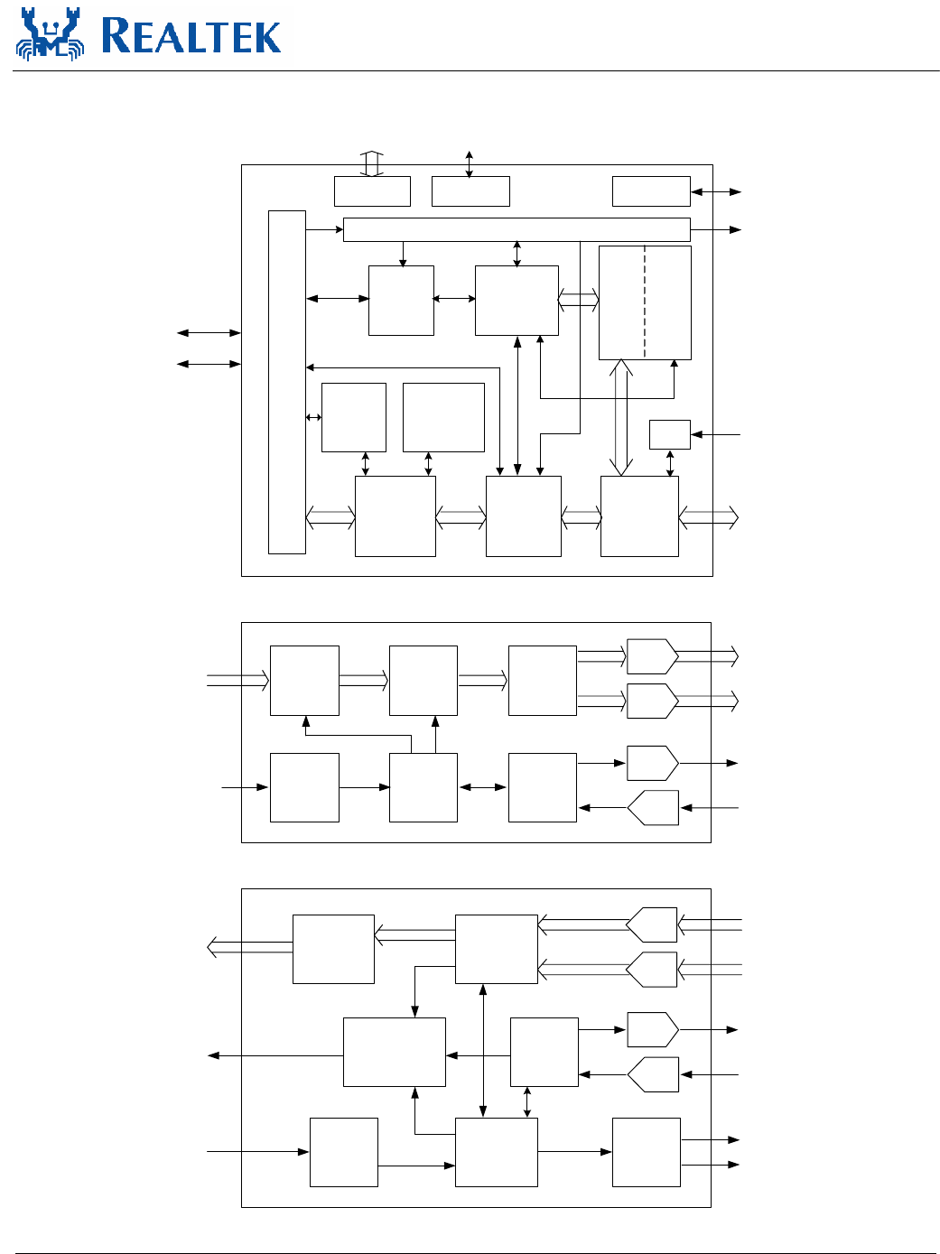
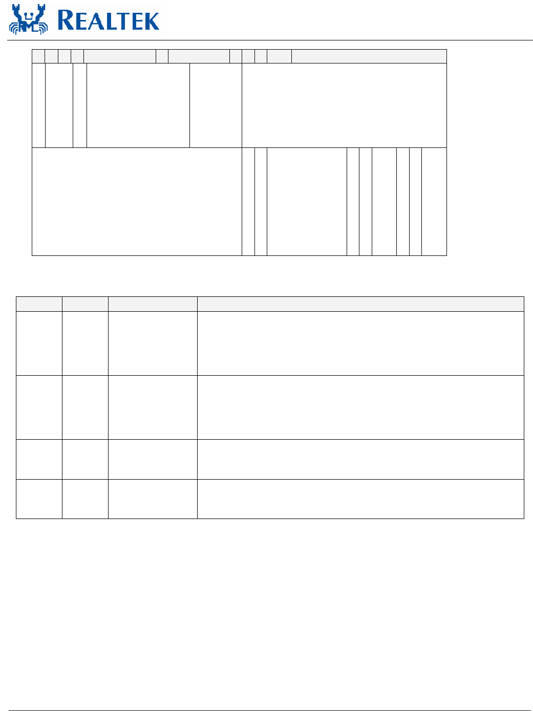
4. Block Diagram
MAC/BBP
Interface
Interrupt
Control
Logic
FIFO
Transmit/
Receive
Logic
Interface
RTS, CTS,
ACK Frame
Generator
FIFO
Control
Logic
Frame Type
Discriminator
Power and TX/RX Timing Control Logic
SIE + Register
Frame Length
Register
EEPROM
Interface LED Driver
Scrambler
TXI
MAC
BBP, TX Section
CCA/
NAV From BBP
WEP/
TKIP/
AES
Engine
Checksum
Logic
Serial
Control Radio and
Synthesizer
Control
Coding Digital
Filter TXQ
TXDET
TXAGC
TX AGC
Control
Descrambler
RXI
MAC/BBP
Interface Decoding
ADC
RXQ
DAC
RSSI
RXAGC
RX AGC
Control
ADC
ADC
Clear Channel
Assessment/
Signal Quality
Antenna
Diversity
Control
TX State
Machine
Register
From
MAC
RX State
Machine
Register
From
MAC
To MAC
D+
D-
BBP, RX Section
MAC/BBP
Interface DAC
ADC
DAC
DAC
ANTSELB
ANTSEL
Figure 1. Block Diagram
RTL8187B
Datasheet
Wireless LAN Network Interface Controller 6 Track ID: JATR-1076-21 Rev. 1.0
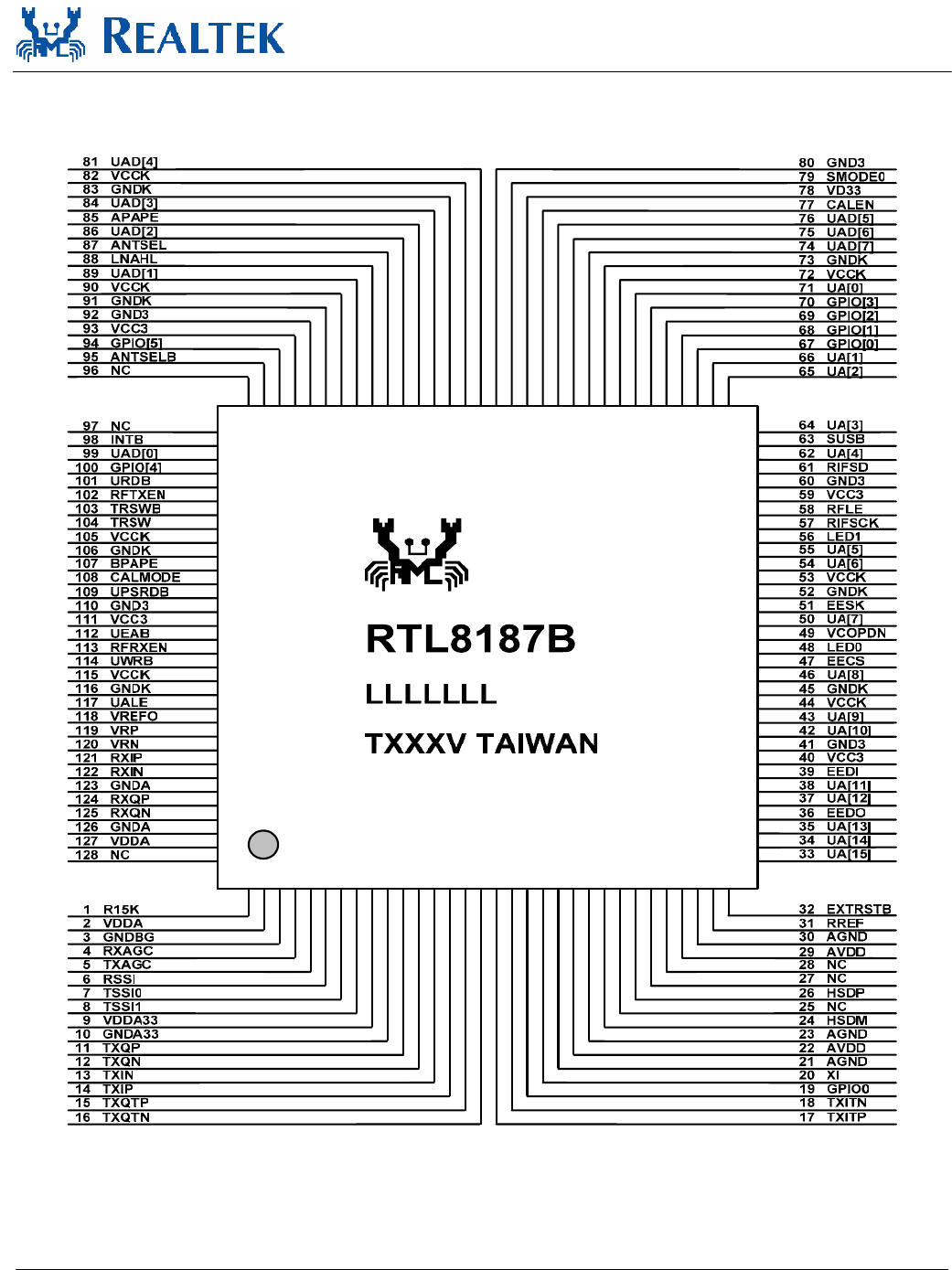
6. Pin Descriptions
In order to reduce pin count, and therefore size and cost, some pins have multiple functions. In such cases,
the functions are separated with a ‘/’ symbol. Refer to the Pin Assignments diagram on page 5 for a
graphical representation.
The following signal type codes are used in the tables:
I: Input.
O: Output
T/S: Tri-State bi-directional input/output pin.
S/T/S: Sustained Tri-State.
O/D: Open Drain.
6.1.
USB Transceiver Interface
Table 1. USB Transceiver Interface
Symbol Type Pin No Description
HSDP I/O 26 High speed USB D+ signal
HSDM I/O 24 High speed USB D- signal
RREF N/A 31 External Reference. Requires 1% precision 6.25K resistor to ground
6.2.
EEPROM Interface
Table 2. EEPROM Interface
Symbol Type Pin No Description
EESK O 51 EESK in 93C46 (93C56) programming or auto-load mode.
EEDI O 39 EEDI in 93C46 (93C56) programming or auto-load mode.
EEDO I/O 36 EEDO in 93C46 (93C56) programming or auto-load mode.
EECS O 47 EEPROM Chip Select. 93C46 (93C56) chip select.
6.3.
Power Pins
Table 3. Power Pins
Symbol Type Pin No Description
VCC3 P 40, 59, 78, 93, 111 +3.3V (Digital).
AVDD P 2, 9, 22, 29, 127 +3.3V (Analog).
VCCK P 44, 53, 72, 82, 90, 105,
115
+1.5V.
GNDK P 41, 45, 52, 60, 73, 80,
83, 91, 92, 106, 110,
116
Ground (Digital).
AGND P 3, 10, 21, 23, 30, 123,
126
Ground (Analog).

RTL8187B
Datasheet
Wireless LAN Network Interface Controller 7 Track ID: JATR-1076-21 Rev. 1.0
6.4.
LED Interface
Table 4. LED Interface
Symbol Type Pin No Description
LED0, 1 O 48, 56 LED Pins (Active low)
LEDS1~0 00 01 10 11
LED0 TX/RX TX/RX TX LINK/ACT
LED1 Infrastructure LINK RX Infrastructure
During power down mode, the LED signals are logic high.
6.5.
Attachment Unit Interface
6.5.1. RTL8225 RF Chipset
Table 5. Attachment Unit Interface
Symbol Type Pin No Description
RIFSCK O 57 Serial Clock Output.
For the RTL8225 RF chipset, all operation mode switching and register setting is
done via a 4-wire serial interface.
RIFSD I/O 61 Serial Data Input/Output.
RFLE O 58 Serial Enable control.
CALEN O 77 Serial Read/Write control.
CALMODE O 108 Receiver Output.
I and Q channel AC coupling high-pass corner frequency selection. The output
function of this pin is not used in the RTL8225 RF chipset.
LNA_HL O 88 Not used in the RTL8225 RF chipset.
ANTSEL O 87 Antenna Select.
The antenna detects signal change states as the receiver switches from antenna to
antenna during the acquisition process in antenna diversity mode. This is a
complement for ANTSELB for differential drive of antenna switches.
ANTSELB O 95 Antenna Select B.
The antenna detects signal change states as the receiver switches from antenna to
antenna during the acquisition process in the antenna diversity mode. This is a
complement for ANTSEL for differential drive of antenna switches.
TRSW
TRSWB
O
O
104
103
Transmit/Receive path select.
The TRSW select signal controls the direction of the Transmit/Receive switch.
VCOPDN O 49 Output Pin as shutdown mode select digital input.
A_PAPE O 85 2.4GHz Transmit Power Amplifier Power Enable.
B_PAPE O 107 Not used in the RTL8225 RF chipset.
RFTXEN O 102 Not used in the RTL8225 RF chipset.
RFRXEN O 113 Not used in the RTL8225 RF chipset.
GPIO0 O 67 General purpose input/output pin.
GPIO1 O 68 General purpose input/output pin.
GPIO2 O 69 General purpose input/output pin.
GPIO3 O 70 General purpose input/output pin.

RTL8187B
Datasheet
Wireless LAN Network Interface Controller 8 Track ID: JATR-1076-21 Rev. 1.0
Symbol Type Pin No Description
GPIO4 O 100 General purpose input/output pin.
GPIO5 O 94 General purpose input/output pin.
VREFO X 118 Not used in the RTL8225 RF chipset.
VRP X 119 Not used in the RTL8225 RF chipset.
VRN X 120 Not used in the RTL8225 RF chipset.
RXIP
RXIN
I
I
121
122
Receive (Rx) In-phase Analog Data.
RXQP
RXQN
I
I
124
125
Receive (Rx) Quadrature-phase Analog Data.
RXAGC I 4 Not used in the RTL8225 RF chipset.
TXAGC O 5 Not used in the RTL8225 RF chipset.
RSSI I 6 Analog Input to the Receive Power A/D Converter for Receive AGC Control.
TSSI0 I 7 Input to the Transmit Power A/D Converter for 2.4GHz Transmit AGC Control.
TSSI1 I 8 Not used in the RTL8225 RF chipset.
TXQP
TXQN
I
I
11
12
Not used in the RTL8225 RF chipset.
TXIP
TXIN
O
O
14
13
Not used in the RTL8225 RF chipset.
TXQTP
TXQTN
O
O
15
16
Transmit (TX) Quadrature-phase Analog Data.
TXITP
TXITN
O
O
17
18
Transmit (TX) In-phase Analog Data.
6.5.2. RTL8255 RF Chipset
Table 6. RTL8255 RF Chipset
Symbol Type Pin No Description
RIFSCK O 57 Serial Clock Output.
For the RTL8255 RF chipset, all operation mode switching and register setting is
done via a 3-wire serial interface.
RIFSD O 61 Serial Data Input/Output.
RFLE O 58 Serial Enable control.
CALEN X 77 Not used in the RTL8255 RF chipset.
CALMODE O 108 Receiver Output.
I and Q channel AC coupling high-pass corner frequency selection. The output
function of this pin is not used in the RTL8255 RF chipset.
LNAHL O 88 Not used in the RTL8255 RF chipset.
ANTSEL
ANTSELB
O
O
87
95
Antenna Select.
The antenna detects signal change states as the receiver switches from antenna to
antenna during the acquisition process in antenna diversity mode.
TRSW
TRSWB
O
O
104
103
Transmit/Receive path select.
The TRSW select signal controls the direction of the Transmit/Receive switch.
VCOPDN O 49 Not used in the RTL8255 RF chipset.
APAPE O 85 2.4GHz Transmit Power Amplifier Power Enable.
BPAPE O 107 5GHz Transmit Power Amplifier Power Enable.

RTL8187B
Datasheet
Wireless LAN Network Interface Controller 9 Track ID: JATR-1076-21 Rev. 1.0
Symbol Type Pin No Description
RFTXEN O 102 Not used in the RTL8255 RF chipset.
RFRXEN O 113 Not used in the RTL8255 RF chipset.
GPIO[0] O 67 General purpose input/output pin.
GPIO[1] O 68 General purpose input/output pin.
GPIO[2] O 69 General purpose input/output pin.
GPIO[3] O 70 General purpose input/output pin.
GPIO[4] O 100 General purpose input/output pin.
GPIO[5] O 94 General purpose input/output pin.
VREFO X
118 Not used in the RTL8255 RF chipset.
VRP X 119 Not used in the RTL8255 RF chipset.
VRN X 120 Not used in the RTL8255 RF chipset.
RXIP
RXIN
I
I
121
122
Receive (Rx) In-phase Analog Data.
RXQP
RXQN
I
I
124
125
Receive (Rx) Quadrature-phase Analog Data.
RXAGC O 4 Not used in the RTL8255 RF chipset.
TXAGC O 5 Not used in the RTL8255 RF chipset.
RSSI I 6 Analog Input to the Receive Power A/D Converter for Receive AGC Control.
TSSI0 I 7 Input to the Transmit Power A/D Converter for 2.4GHz Transmit AGC Control.
TSSI1 I 8 Input to the Transmit Power A/D Converter for 5GHz Transmit AGC Control.
TXQP
TXQN
O
O
11
12
Transmit (TX) Quadrature-phase Analog Data.
TXIP
TXIN
O
O
14
13
Transmit (TX) In-phase Analog Data.
TXQTP
TXQTN
O
O
15
16
Not used in the RTL8255 RF chipset.
TXITP
TXITN
O
O
17
18
Not used in the RTL8255 RF chipset.
6.6.
Clock and Other Pins
Table 7. Clock and Other Pins
Symbol Type Pin No Description
R15K I/O 1 This pin must be pulled low by a 15K Ω resistor.
XI I 20 40MHz clock Input.
EXTRSTB I 32 Pull high 3.3V. If pulled low, the whole chip will be reset.

RTL8187B
Datasheet
Wireless LAN Network Interface Controller 10 Track ID: JATR-1076-21 Rev. 1.0
7. CPU Access to Endpoint Data
7.1.
Control Transfer
Control transfers configure and send commands to a device. Because they are so important, they employ
extensive USB error checking. The host reserves a portion of each USB frame for control transfers. Control
transfers consist of two or three stages. The SETUP stage contains eight bytes of USB control data. An
optional DATA stage contains more data, if required. The STATUS stage allows the device to indicate
successful completion of a control operation.
7.2.
Bulk Transfer
Bulk data is bursty, traveling in packets of 8, 16, 32, or 64 bytes at full speed, or at 512 bytes at high speed.
Bulk data has guaranteed accuracy due to an automatic retry mechanism for erroneous data. The host
schedules transmission of bulk packets when there is available bus time.
RTL8187B
Datasheet
Wireless LAN Network Interface Controller 11 Track ID: JATR-1076-21 Rev. 1.0
8. USB Request
8.1.
Get Descriptor-Device
Table 8. Get Descriptor-Device
Setup Transaction
BmReq bReq wValueL wValueH wIndexL wIndexH wLengthL wLengthH
80 06 00 01 00 00 Lengh_L Length_H
High Speed Data Transaction
DATA0 DATA1 DATA2 DATA3 DATA4 DATA5 DATA6 DATA7
12 01 00 02 00 00 00 40
DA 0B 87 81 00 01 01 02
03 01
Full Speed Data Transaction
DATA0 DATA1 DATA2 DATA3 DATA4 DATA5 DATA6 DATA7
12 01 10 01 00 00 00 40
DA 0B 87 81 00 01 01 02
03 01
8.2.
Get Descriptor-Device Qualifier (High Speed)
Table 9. Get Descriptor- Device Qualifier (High Speed)
Setup Transaction
BmReq bReq wValueL wValueH wIndexL wIndexH wLengthL wLengthH
80 06 00 06 00 00 Lengh_L Length_H
Data Transaction
DATA0 DATA1 DATA2 DATA3 DATA4 DATA5 DATA6 DATA7
0A 06 00 02 00 00 00 40
01 00
RTL8187B
Datasheet
Wireless LAN Network Interface Controller 12 Track ID: JATR-1076-21 Rev. 1.0
8.3.
Get Descriptor-Configuration
Table 10. Get Descriptor-Configuration
Setup Transaction
BmReq bReq wValueL wValueH wIndexL wIndexH wLengthL wLengthH
80 06 00 02 00 00 Length_L Length_H
High Speed Data Transaction
DATA0 DATA1 DATA2 DATA3 DATA4 DATA5 DATA6 DATA7
09 02 51 00 01 01 04 80
FA 09 04 00 00 09 FF FF
FF 02 07 05 83 02 00 02
00 07 05 04 02 00 02 00
07 05 05 02 00 02 00 07
05 06 02 00 02 00 07 05
07 02 00 02 00 07 05 89
02 00 02 00 07 05 0A 02
00 02 00 07 05 0B 02 00
02 00 07 05 0C 02 00 02
00
Full Speed Data Transaction
DATA0 DATA1 DATA2 DATA3 DATA4 DATA5 DATA6 DATA7
09 02 51 00 01 01 04 80
FA 09 04 00 00 09 FF FF
FF 02 07 05 83 02 40 00
00 07 05 04 02 40 00 00
07 05 05 02 40 00 00 07
05 06 02 40 00 00 07 05
07 02 40 00 00 07 05 89
02 40 00 00 07 05 0A 02
40 00 00 07 05 0B 02 40
00 00 07 05 0C 02 40 00
00
RTL8187B
Datasheet
Wireless LAN Network Interface Controller 13 Track ID: JATR-1076-21 Rev. 1.0
8.4.
Get Descriptor-String Index 0
Table 11. Get Descriptor-String Index 0
Setup Transaction
BmReq bReq wValueL wValueH wIndexL wIndexH wLengthL wLengthH
80 06 00 03 00 00 Lengh_L Length_H
Data Transaction
DATA0 DATA1 DATA2 DATA3 DATA4 DATA5 DATA6 DATA7
04 03 09 04 - - - -
8.5.
Get Descriptor-String Index 1
Table 12. Get Descriptor-String Index 1
Setup Transaction
BmReq bReq wValueL wValueH wIndexL wIndexH wLengthL wLengthH
80 06 01 03 09 04 Lengh_L Length_H
Data Transaction
DATA0 DATA1 DATA2 DATA3 DATA4 DATA5 DATA6 DATA7
10 03 52 00 65 00 61 00
6C 00 74 00 65 00 6B 00
8.6.
Get Descriptor-String Index 2
Table 13. Get Descriptor-String Index 2
Setup Transaction
BmReq bReq wValueL wValueH wIndexL wIndexH wLengthL wLengthH
80 06 02 03 09 04 Lengh_L Length_H
Data Transaction
DATA0 DATA1 DATA2 DATA3 DATA4 DATA5 DATA6 DATA7
2B 03 52 00 54 00 4C 00
38 00 31 00 38 00 37 00
42 00 20 00 57 00 4C 00
41 00 4E 00 20 00 41 00
64 00 6` 00 70 00 74 00
65 00 72
RTL8187B
Datasheet
Wireless LAN Network Interface Controller 14 Track ID: JATR-1076-21 Rev. 1.0
8.7.
Get Descriptor-String Index 3
Table 14. Get Descriptor-String Index 3
Setup Transaction
BmReq bReq wValueL wValueH wIndexL wIndexH wLengthL wLengthH
80 06 03 03 09 04 Lengh_L Length_H
Data Transaction
DATA0 DATA1 DATA2 DATA3 DATA4 DATA5 DATA6 DATA7
1A 03 30 00 30 00 65 00
30 00 34 00 63 00 30 00
30 00 30 00 30 00 30 00
31 00
8.8.
Get Descriptor-String Index 4
Table 15. Get Descriptor-String Index 4
Setup Transaction
BmReq bReq wValueL wValueH wIndexL wIndexH wLengthL wLengthH
80 06 04 03 09 04 Lengh_L Length_H
Data Transaction
DATA0 DATA1 DATA2 DATA3 DATA4 DATA5 DATA6 DATA7
2C 03 57 00 69 00 72 00
65 00 6C 00 65 00 73 00
73 00 20 00 4E 00 65 00
74 00 77 00 6F 00 72 00
6B 00 20 00 43 00 61 00
72 00 64 00
RTL8187B
Datasheet
Wireless LAN Network Interface Controller 15 Track ID: JATR-1076-21 Rev. 1.0
8.9.
Get Descriptor-String Index 5
Table 16. Get Descriptor-String Index 5
Setup Transaction
BmReq bReq wValueL wValueH wIndexL wIndexH wLengthL wLengthH
80 06 05 03 09 04 Lengh_L Length_H
Data Transaction
DATA0 DATA1 DATA2 DATA3 DATA4 DATA5 DATA6 DATA7
30 03 55 00 53 00 42 00
20 00 48 00 53 00 20 00
48 00 65 00 72 00 69 00
61 00 6C 00 20 00 43 00
6F 00 6E 00 76 00 65 00
72 00 74 00 65 00 72 00
8.10.
Get Descriptor-Other Speed Configuration
Table 17. Get Descriptor-Other Speed Configuration
Setup Transaction
BmReq bReq wValueL wValueH wIndexL wIndexH wLengthL wLengthH
80 06 00 07 00 00 Lengh_L Length_H
High Speed Data Transaction
DATA0 DATA1 DATA2 DATA3 DATA4 DATA5 DATA6 DATA7
09 07 51 00 01 01 04 80
FA 09 04 00 00 09 FF FF
FF 02 07 05 83 02 00 02
00 07 05 04 02 00 02 00
07 05 05 02 00 02 00 07
05 06 02 00 02 00 07 05
07 02 00 02 00 07 05 89
02 00 02 00 07 05 0A 02
00 02 00 07 05 0B 02 00
02 00 07 05 0C 02 00 02
00
RTL8187B
Datasheet
Wireless LAN Network Interface Controller 16 Track ID: JATR-1076-21 Rev. 1.0
Full Speed Data Transaction
DATA0 DATA1 DATA2 DATA3 DATA4 DATA5 DATA6 DATA7
09 07 51 00 01 01 04 80
FA 09 04 00 00 09 FF FF
FF 02 07 05 83 02 40 00
00 07 05 04 02 40 00 00
07 05 05 02 40 00 00 07
05 06 02 40 00 00 07 05
07 02 40 00 00 07 05 89
02 40 00 00 07 05 0A 02
40 00 00 07 05 0B 02 40
00 00 07 05 0C 02 40 00
00
8.11.
Set Address
Table 18. Set Address
Setup Transaction
BmReq bReq wValueL wValueH wIndexL wIndexH wLengthL wLengthH
00 05 addrL addrH 00 00 00 00
Note: No data transaction.
8.12.
Set Interface 0
Table 19. Set Interface 0
Setup Transaction
BmReq bReq wValueL wValueH wIndexL wIndexH wLengthL wLengthH
01 0B 00 00 00 00 00 00
Note: No data transaction.
8.13.
Set Feature Device
Table 20. Set Feature Device
Setup Transaction
BmReq bReq wValueL wValueH wIndexL wIndexH wLengthL wLengthH
00 03 01 00 00 00 00 00
Note: No data transaction.
RTL8187B
Datasheet
Wireless LAN Network Interface Controller 17 Track ID: JATR-1076-21 Rev. 1.0
8.14.
Clear Feature Device
Table 21. Clear Feature Device
Setup Transaction
BmReq bReq wValueL wValueH wIndexL wIndexH wLengthL wLengthH
00 01 01 00 00 00 00 00
Note: No data transaction.
8.15.
Set Config 0
Table 22. Set Config 0
Setup Transaction
BmReq bReq wValueL wValueH wIndexL wIndexH wLengthL wLengthH
00 09 00 02 00 00 00 00
Note: No data transaction.
8.16.
Set Config 1
Table 23. Set Config 1
Setup Transaction
BmReq bReq wValueL wValueH wIndexL wIndexH wLengthL wLengthH
00 09 01 00 00 00 00 00
Note: No data transaction.

RTL8187B
Datasheet
Wireless LAN Network Interface Controller 18 Track ID: JATR-1076-21 Rev. 1.0
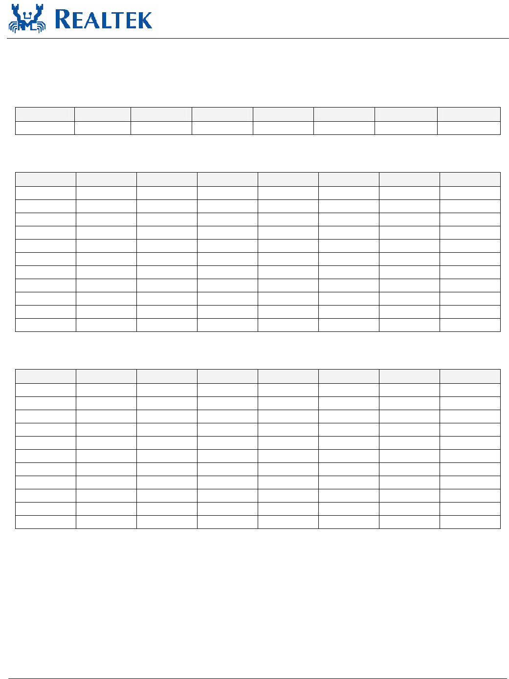
9. EEPROM (93C46 or 93C56) Contents
The RTL8187B supports the attachment of an external EEPROM. The 93C46 is a 1Kbit EEPROM (the
93C56 is a 2Kbit EEPROM). The EEPROM interface provides the ability for the RTL8187B to read from,
and write data to, an external serial EEPROM device. If the EEPROM is not present, the RTL8187B
initialization uses default values for the Operational Registers. Software can read and write to the
EEPROM using “bit-bang” accesses via the 9346CR Register.
Although it is actually addressed by words, its contents are listed below by bytes for convenience. After the
initial power on or auto-load command in the 9346CR, the RTL8187B performs a series of EEPROM read
operations from the 93C46 (93C56).
Note: It is suggested to obtain Realtek approval before changing the default settings of the EEPROM.
Table 24. EEPROM (93C46 or 93C56) Contents
Bytes Contents Description
00h 29h
01h 81h
These 2 bytes contain the ID code word for the RTL8187B. The RTL8187B will load
the contents of the EEPROM into the corresponding location if the ID word (8129h) is
correct.
02h-03h VID USB Vendor ID.
04h-05h DID USB Device ID.
06h ChannelPlan Channel Plan: Map of channels to be scanned.
07h Reserved -
08h Reserved -
09h Version Bit [7:6] Interface Selection
00 : USB
01 : Mini Card
02 : Reserved
03 : Reserved
Bit [5:0] The EEPROM version.
0Ah Tx Power Base Tx power of the serving base station.
0Bh Reserved -
0Ch RFChipID RF Chip ID.
The identifier of the RF chip.
0Dh CONFIG3 RTL8187B Configuration register 3.
Operational register FF59h.
0Eh~13h MAC Address MAC Address.
After the auto-load command or a hardware reset, the RTL8187B loads MAC
Addresses to IDR0~IDR5 of the I/O registers of the RTL8187B.
14h TxPower12 Transmit Power Level for 802.11b(g)-defined channel_ID 12
(center frequency=2467MHz).
15h CONFIG1 RTL8187B Configuration register 1.
Operational register FF52h.
Bit[5:2] : USB receive sensitivity
16h~17h CRC 16-bit CRC value of EEPROM content. Reserved for Software use.
18h CONFIG2 RTL8187B Configuration register 2.
Operational register FF53h.

RTL8187B
Datasheet
Wireless LAN Network Interface Controller 19 Track ID: JATR-1076-21 Rev. 1.0
Bytes Contents Description
19h CONFIG4 RTL8187B Configuration register 4.
Operational register FF5Ah.
1Ah~1Dh ANA_PARM Analog Parameter for the RTL8187B.
Operational registers of the RTL8187B are from 54h to 57h.
Reserved. Do not change this field without Realtek approval.
1Eh TESTR RTL8187B Test Mode Register.
Operational register FF5Bh.
Reserved. Do not change this field without Realtek approval.
1Fh CONFIG5 RTL8187B Configuration register 5.
Operational register FFD8h.
20h TxPower36 Transmit Power Level for 802.11a-defined channel_ID 36
(Center frequency=5180MHz).
21h TxPower40 Transmit Power Level for 802.11a-defined channel_ID 40
(Center frequency=5200MHz).
22h TxPower44 Transmit Power Level for 802.11a-defined channel_ID 44
(Center frequency=5220MHz).
23h TxPower48 Transmit Power Level for 802.11a-defined channel_ID 48
(Center frequency=5240MHz).
24h TxPower52 Transmit Power Level for 802.11a-defined channel_ID 52
(Center frequency=5260MHz).
25h TxPower56 Transmit Power Level for 802.11a-defined channel_ID 56
(Center frequency=5280MHz).
26h TxPower60 Transmit Power Level for 802.11a-defined channel_ID 60
(Center frequency=5300MHz).
27h TxPower64 Transmit Power Level for 802.11a-defined channel_ID 64
(Center frequency=5320MHz).
28h TxPower149 Transmit Power Level for 802.11a-defined channel_ID 149
(Center frequency=5745MHz).
29h TxPower153 Transmit Power Level for 802.11a-defined channel_ID 153
(Center frequency=5765MHz).
2Ah TxPower157 Transmit Power Level for 802.11a-defined channel_ID 157
(Center frequency=5785MHz).
2Bh TxPower161 Transmit Power Level for 802.11a-defined channel_ID 161
(Center frequency=5805MHz).
2Ch TxPower1 Transmit Power Level for 802.11b(g)-defined channel_ID 1
(center frequency=2412MHz).
2Dh TxPower2 Transmit Power Level for 802.11b(g)-defined channel_ID 2
(center frequency=2417MHz).
2Eh TxPower3 Transmit Power Level for 802.11b(g)-defined channel_ID 3
(center frequency=2422MHz).
2Fh TxPower4 Transmit Power Level for 802.11b(g)-defined channel_ID 4
(center frequency=2427MHz).
30h TxPower5 Transmit Power Level for 802.11b(g)-defined channel_ID 5
(center frequency=2432MHz).
31h TxPower6 Transmit Power Level for 802.11b(g)-defined channel_ID 6
(center frequency=2437MHz).

RTL8187B
Datasheet
Wireless LAN Network Interface Controller 20 Track ID: JATR-1076-21 Rev. 1.0
Bytes Contents Description
32h-35h ANA_PARM2 Analog Parameter 2 for RTL8187B.
Operational registers for the RTL8187B are 60h to 63h.
Reserved. Do not change this field without Realtek approval.
36h TxPower11 Transmit Power Level for 802.11b(g)-defined channel_ID 11
(center frequency=2462MHz).
37h Optional functions Bit[1:0]: Suspend pin behavior.
00b: Default pull high
01b: Default pill low
10b: Functions as a PME# signal
Bit[2]: USB remote wake up function.
0: No remote wake up feature for RTL8187B
1: Remote wake up feature for RTL8187B
Bit[3] : UART Support.
0: No UART interface support
1: UART interface support
Bit[5:4]: Response default serial number.
00b: Respond serial number from EEPROM
01b: Respond serial number from internal ROM, 00 E0 4C 00 00 01
Others : Reserved
Bit[6] : Device Power.
0: Bus power
1: Self power
38h TxPower13 Transmit Power Level for 802.11b(g)-defined channel_ID 13
(center frequency=2472MHz).
39h TxPower14 Transmit Power Level for 802.11b(g)-defined channel_ID 14
(center frequency=2484MHz).
3Ah-73h Manufacture String
&
Product String
Manufacture String and Product String:Those bits specify both manufacturer’s
information and device’s information for the USB standard request.
Maximum two strings total length are 58 bytes.
74h-79h - Reserved.
7Ah TxPower7 Transmit Power Level for 802.11b(g)-defined channel_ID 7
(center frequency=2442MHz).
7Bh TxPower8 Transmit Power Level for 802.11b(g)-defined channel_ID 8
(center frequency=2447MHz).
7Ch TxPower9 Transmit Power Level for 802.11b(g)-defined channel_ID 9
(center frequency=2452MHz).
7Dh TxPower10 Transmit Power Level for 802.11b(g)-defined channel_ID 10
(center frequency=2457MHz).
7Eh CustomerID BIT[0-7]: CustomerID, 0x00 and 0xFF is reserved for Realtek.
7Fh SW Antenna
Diversity
BIT[0:1]: 01b enables SW Antenna Diversity.
BIT[2:3]: 01b is default antenna.
RTL8187B
Datasheet
Wireless LAN Network Interface Controller 21 Track ID: JATR-1076-21 Rev. 1.0
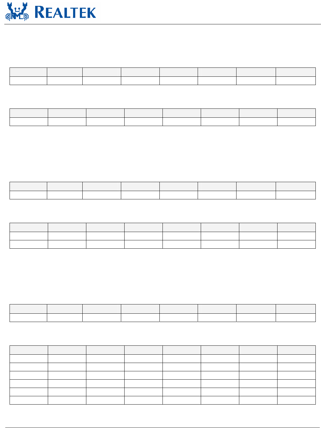
9.1.
EEPROM Registers Summary
Table 25. EEPROM Registers Summary
Address Name Type Bit7 Bit6 Bit5 Bit4 Bit3 Bit2 Bit1 Bit0
FF00h-
FF05h IDR0 – IDR5 R/W*
R LEDS1 LEDS0 USB Receive Sensitivity - -
FF52h CONFIG1 W* LEDS1 LEDS0 USB Receive Sensitivity - -
R LCK - - - -
PAPE
_sign
PAPE
_time
FF53h CONFIG2
W* - - - - -
PAPE
_sign
PAPE
_time
FF54h-
FF57h ANA_PARM R/W** 32-bit Read Write
R - PARM_En Magic - - - - -
FF59h CONFIG3 W* - PARM_En Magic - - - - -
R - - - LWPME - LWPTN -
FF5Ah CONFIG4 W* - - - LWPME - LWPTN -
FF5Bh TESTR 8-bit Read Write
FF60h-
FF63h ANA_PARM2 R/W 32-bit Read Write
FFD8h CONFIG5 R/W** - - - - - - LANWake -
Note 1: Registers marked 'W*' can be written only if bits EEM1=EEM0=1.
Note 2: Registers marked 'W**' can be written only if bits EEM1:0=[1:1] and
CONFIG3<PARM_EN>= 0.
9.2.
EEPROM Power Management Registers Summary
Table 26. EEPROM Power Management Registers Summary
Configuration
Space Offset
Name Type Bit7 Bit6 Bit5 Bit4 Bit3 Bit2 Bit1 Bit0
52h R Aux_I_b1 Aux_I_b0 DSI Reserved PMECLK Version
53h
PMC
R PME_D3cold PME_D3hot PME_D2 PME_D1 PME_D0 D2 D1 Aux_I_b2

RTL8187B
Datasheet
Wireless LAN Network Interface Controller 22 Track ID: JATR-1076-21 Rev. 1.0
10. USB Packet Buffering
The RTL8187B incorporates two independent FIFOs for transferring data to/from the system interface and
from/to the network. The FIFOs provide temporary storage of data, freeing the host system from the
real-time demands of the network.
The way in which the FIFOs are emptied and filled is controlled by the FIFO threshold values in the
Receive Configuration registers. These values determine how full or empty the FIFOs must be before the
device requests the bus. Once the RTL8187B requests the bus, it will attempt to empty or fill the FIFOs as
allowed by the respective MXDMA settings in the Transmit Configuration and Receive Configuration
registers.
10.1.
Transmit Buffer Manager
The buffer management scheme used on the RTL8187B allows quick, simple, and efficient use of the frame
buffer memory. The buffer management scheme uses separate buffers and descriptors for packet
information. This allows effective transfers of data to the transmit buffer manager by simply transferring
the descriptor information to the transmit queue.
The Tx Buffer Manager DMA’s packet data from system memory and places it in the 3.5KB transmit FIFO,
and pulls data from the FIFO to send to the Tx MAC. Multiple packets may be present in the FIFO,
allowing packets to be transmitted with Short InterFrame (SIF) space. Additionally, once the RTL8187B
requests the bus, it will attempt to fill the FIFO as allowed by the MXDMA setting.
The Tx Buffer Manager process also supports priority queuing of transmit packets. It handles this by
drawing from two separate descriptor lists to fill the internal FIFO. If packets are available in the high
priority queues, they will be loaded into the FIFO before those of low priority.
10.2.
Receive Buffer Manager
The Rx Buffer Manager uses the same buffer management scheme as used for transmits. The Rx Buffer
Manager retrieves packet data from the Rx MAC and places it in the 4KB receive data FIFO, and pulls data
from the FIFO for DMA to system memory. The receive FIFO is controlled by the FIFO threshold value in
RXFTH. This value determines the number of long words written into the FIFO from the MAC unit before
a DMA request for system memory occurs. Once the RTL8187B gets the bus, it will continue to transfer the
long words from the FIFO until the data in the FIFO is less than one long word, or has reached the end of the
packet, or the max DMA burst size is reached, as set in MXDMA.
10.3.
Packet Recognition
The Rx packet filter and recognition logic allows software to control which packets are accepted, based on
destination address and packet type. Address recognition logic includes support for broadcast, multicast
hash, and unicast addresses. The packet recognition logic includes support for WOL and programmable
pattern recognition.
RTL8187B
Datasheet
Wireless LAN Network Interface Controller 23 Track ID: JATR-1076-21 Rev. 1.0
11. Functional Description
11.1.
Transmit & Receive Operations
The RTL8187B supports a new descriptor-based buffer management that will significantly lower host CPU utilization. The
RTL8187B supports transmit descriptor and receive descriptor in memory. Each OUT packet contains 3-double-word transmit
descriptors and each IN packet contains 4-double-word receive descriptors.
11.1.1. Transmit
Tx Descriptor Format
Table 27. Tx Descriptor Format
31 30 29 28 27 26 25 24 23 22 21 20 19 18 17 16 15 14 13 12 11 10 9 8 7 6 5 4 3 2 1 0
O
W
N
=
1
D
M
A
O
K
F
S
L
S
TXRATE
(4 bits)
R
T
S
E
N
RTSRATE
(4 bits)
C
T
S
E
N
M
O
R
E
F
R
A
G
S
P
L
C
P
N
O
_
E
N
C
R
Y
P
T
BSSID
_NO
TPKTSIZE (12 bits) Offset 0
L
E
N
G
E
X
T
Length (15 bits)
RTSDUR (16 bits)
Offset 4
TX_BUFFER_ADDRESS Offset 8
DURATION (16 bits) M
I
C
_
C
A
L
RSVD
(3 bits)
Frame_Length (12 bits) Offset 12
NEXT_TX_DESCRIPTOR_ADDRESS Offset 16
RATE_FALL
BACK_LIMIT
(5 bits)
RTS_RATE
_FALL
BACK_LIM
IT (4 bits)
RSVD
(4bits)
P
I
F
S
N
O
_
A
C
M
R
T
_
D
B
RETRY_LIMIT (8 bits) RTSAGC (8 bits) Offset 20
RTL8187B
Datasheet
Wireless LAN Network Interface Controller 24 Track ID: JATR-1076-21 Rev. 1.0
31 30 29 28 27 26 25 24 23 22 21 20 19 18 17 16 15 14 13 12 11 10 9 8 7 6 5 4 3 2 1 0
R
S
V
D
SPC A
N
T
E
N
N
A
AGC (8 bits) RSVD
(4bits)
DELAY_BOUND (16 bits) Offset 24
FRAG_QSIZE (16 bits) E
N
_
P
M
P
D
E
N
_
B
C
K
E
Y
BCKEY (6 bits) P
T
_
E
N
T
P
C
_
E
N
TPC
_PO
LAR
ITY
T
P
C
_
D
E
S
E
N
R
S
V
D
HW
Leng
thSel
ect
Offset 28
Table 28. Tx Status Descriptor
Offset# Bit# Symbol Description
0 31 OWN Ownership.
When set, this bit indicates that the descriptor is owned by the NIC, and the
data relative to this descriptor is ready to be transmitted. When cleared, it
indicates that the descriptor is owned by the host system. The NIC clears this
bit when the relative buffer data is transmitted. In this case, OWN=1.
0 30 DMA OK DMA OK.
Set by the driver, reset by the RTL8187B when TX DMA OK. If IMR’s
corresponding bit is set and the driver sets this bit, the RTL8187B resets this
bit and issues an interrupt right after DMA OK of the last segment (LS). If not,
the RTL8187B just resets this bit without asserting an interrupt.
0 29 FS First Segment Descriptor.
When set, this bit indicates that this is the first descriptor of a Tx packet, and
that this descriptor is pointing to the first segment of the packet.
0 28 LS Last Segment Descriptor.
When set, indicates that this is the last descriptor of a Tx packet, and this
descriptor is pointing to the last segment of the packet.
RTL8187B
Datasheet
Wireless LAN Network Interface Controller 25 Track ID: JATR-1076-21 Rev. 1.0
Offset# Bit# Symbol Description
Tx Rate.
These five bits indicate the current frame’s transmission rate.
Bit 27 Bit 26 Bit 25 Bit 24
1Mbps 0 0 0 0
2Mbps 0 0 0 1
5.5Mbps 0 0 1 0
11Mbps 0 0 1 1
6Mbps 0 1 0 0
9Mbps 0 1 0 1
12Mbps 0 1 1 0
18Mbps 0 1 1 1
24Mbps 1 0 0 0
36Mbps 1 0 0 1
48Mbps 1 0 1 0
54Mbps 1 0 1 1
0 27:24 TXRATE
Reserved All other combinations
0 23 RTSEN RTS Enable.
Set to 1 indicates that an RTS/CTS handshake shall be performed at the
beginning of any frame exchange sequence where the frame is of type Data or
Management, the frame has an unicast address in the Address1 field, and the
length of the frame is greater than RTSThreshold.
RTS Rate.
These four bits indicate the RTS frame’s transmission rate before transmitting
the current frame and will be ignored if the RTSEN bit is set to 0.
Bit 22 Bit 21 Bit 20 Bit 19
1Mbps 0 0 0 0
2Mbps 0 0 0 1
5.5Mbps 0 0 1 0
11Mbps 0 0 1 1
6Mbps 0 1 0 0
9Mbps 0 1 0 1
12Mbps 0 1 1 0
18Mbps 0 1 1 1
24Mbps 1 0 0 0
36Mbps 1 0 0 1
48Mbps 1 0 1 0
54Mbps 1 0 1 1
0 22:19 RTSRATE
Reserved All other combinations
0 18 CTSEN CTS Enable.
Both RTSEN and CTSEN set to 1 indicates that the CTS-to-self protection
mechanism will be used.
0 17 MOREFRAG More Fragment.
This bit is set to 1 in all data type frames that have another fragment of the
current packet to follow.
0 16 SPLCP Short Physical Layer Convergence Protocol format.
When set, this bit indicates that a short PLCP preamble will be added to the
header before transmitting the frame.

RTL8187B
Datasheet
Wireless LAN Network Interface Controller 26 Track ID: JATR-1076-21 Rev. 1.0
Offset# Bit# Symbol Description
0 15 NO_ENCRYPT No Encryption.
This packet will be sent out without encryption even if Tx encryption is
enabled.
0 14:12 RSVD Reserved.
0 11:0 TPKTSIZE Transmit Packet Size.
This field indicates the number of bytes required to transmit the frame.
4 31 LENGEXT Length Extension.
This bit is used to supplement the Length field (bits 30:16, offset 4). This bit
will be ignored if the TXRATE is set to 1Mbps, 2Mbps, or 5.5Mbps.
4 30:16 Length PLCP Length: The PLCP length field indicates the number of microseconds
required to transmit the frame.
4 15:0 RTSDUR RTS Duration: These bits indicate the RTS frame’s duration field before
transmitting the current frame and will be ignored if the RTSEN bit is set to 0.
8 31:0 TxBuff 32-bit Transmit Buffer Address.
12 31:16 DURATION Time duration to send this packet plus SIFS and ACK
12 15 MIC_CAL Enable MIC calculation.
12 14:12 RSVD Reserved.
12 11:0 Frame_Length Transmit Frame Length.
This field indicates the length in the Tx buffer, in bytes, to be transmitted.
16 31:0 NTDA 32-bit Address of the Next Transmit Descriptor.
20 31:27 RATE_FALL
BACK_LIMIT
Data Rate Auto Fallback Limit.
20 26:23 RTS_RATE_FALL
BACK_LIMIT
RTS/CTS Rate Auto Fallback Limit.
20 22:19 RSVD Reserved.
20 18 PIFS Setting this bit will cause this frame be sent after PIFS
20 17 NO_ACM No admission control procedure.
This packet will be sent out without being restricted by admission control
procedures. For example, the management type frames shall be sent using the
access category AC_VO without being restricted by admission control
procedures.
20 16 RT_DB Lifetime limited by RETRY_LIMIT (RT_DB=0) or DELAY_BOUND
(RT_DB=1).
20 15:8 RETRY_LIMIT Retry Count Limit.
20 7:0 RTSAGC Tx RTS AGC.
24 31 RSVD Reserved.
24 30:29 SPC Short preamble count.
00: 10 bits
01: 12 bits
10: 14 bits
11: 16 bits
24 28 ANTENNA Tx Antenna.
24 27:20 AGC Tx AGC.
24 19:16 RSVD Reserved.
24 15:0 DELAY_BOUND DELAY BOUND
RTL8187B
Datasheet
Wireless LAN Network Interface Controller 27 Track ID: JATR-1076-21 Rev. 1.0
Offset# Bit# Symbol Description
28 31:16 FRAG_QSIZE Fragmentation Queue Size.
Upon sending the first frame of a fragmentation sequence, the driver writes the
queue size of the entire fragmentation exchange (including the first frame)
here. MAC uses this value when counting down TXOP. This field is valid
when TCR (0x40) duration processing fields are set to mode 1 or 2.
28 15 ENPMPD Enable Power Meter Pre-distortion Packet.
28 14 EN_BCKEY Enable broadcast/multicast key search when using Multiple BSSID
28 13:8 BCKEY Specify key to use in CAM for broadcast/multicast.
28 7 PT_EN Enable Power Tracking.
28 6 TPC_EN Enable TPC.
28 5:4 TPC_POLARITY TPC Polarity Select.
00: Neither increment nor decrement.
01: Increment.
10: Decrement.
11: Reserved.
28 3 TPC_DESEN TPC Descriptor AGC Enable.
0: Use the value of register TPC_TXAGC_OFDM as 54MHz TXAGC Base.
1: Use the value of AGC in the same descriptor as 54MHz TXAGC Base.
28 1:0 HWLengthSelect HW Length Select.
00: No Encryption.
01: RC4 Encryption.
10: AES Encryption.
11: Reserved.
11.1.2. Receive
Rx Descriptor Format
Table 29. Rx Descriptor Format
31 30 29 28 27 26 25 24 23 22 21 20 19 18 17 16 15 14 13 12 11 10 9 8 7 6 5 4 3 2 1 0
O
W
N
=
0
D
M
A
_
O
K
F
S
L
S
RSVD (11 bits)
U
D
R
T
O
K
RTS RC
(7 bits)
Packet RC
(8 bits)
Offset 0
RSVD Offset 4
TX_BUFFER_ADDRESS Offset 8
MPDUExchangeTime (16 bits) RSVD (4
bits)
Frame_Length (12 bits) Offset 12
NEXT_TX_ DESCRIPTOR _ADDRESS Offset 16
RSVD Offset 20
RSVD Offset 24
RSVD Offset 28

RTL8187B
Datasheet
Wireless LAN Network Interface Controller 28 Track ID: JATR-1076-21 Rev. 1.0
Table 30. Rx Status Descriptor
Offset# Bit# Symbol Description
0 31 OWN Ownership.
When set, this bit indicates that the descriptor is owned by the NIC. When clear, it
indicates that the descriptor is owned by the host system. The NIC clears this bit
when the related buffer data has been transmitted. In this case, OWN=0.
0 30 DMA_OK DMA Okay.
0 29 FS First Segment Descriptor.
When set, this bit indicates that this is the first descriptor of a Tx packet, and that
this descriptor is pointing to the first segment of the packet.
0 28 LS Last Segment Descriptor.
When set, this bit indicates that this is the last descriptor of a Tx packet, and that
this descriptor is pointing to the last segment of the packet.
0 27:17 RSVD Reserved.
0 16 UDR FIFO underrun during transmission of this packet.
0 15 TOK Transmit (Tx) OK.
Indicates that a packet exchange sequence has completed successfully.
0 14:8 RTS RC RTS Retry Count. The RTS RC’s initial value is 0. It indicates the number of
retries of RTS.
0 7:0 Packet RC Packet Retry Count.
The RC’s initial value is 0. It indicates the number of retries before a packet was
transmitted properly.
4 31:0 RSVD Reserved.
8 31:0 TxBuff 32-bit Transmit Buffer Address.
12 31:16 MPDUExchange
Time
MPDUExchangeTime corresponds to the just completed MPDU exchange. The
MPDUExchangeTime equals the time required to transmit the MPDU sequence,
i.e., the time required to transmit the MPDU plus the time required to transmit the
expected response frame plus one SIFS.
12 15:12 RSVD Reserved.
12 11:0 Frame_Length Transmit Frame Length.
This field indicates the length in the Tx buffer, in bytes, to be transmitted.
16 31:0 NTDA 32-bit Address of Next Transmit Descriptor.
20 31:0 RSVD Reserved.
24 31:0 RSVD Reserved.
28 31:0 RSVD Reserved.
RTL8187B
Datasheet
Wireless LAN Network Interface Controller 29 Track ID: JATR-1076-21 Rev. 1.0
11.2.
Rx Command
The RTL8187B supports an Rx command queue to feedback the Tx state and beacon interrupt . When the
Command Type (bit[31:30]) is set to 00b, it indicates Tx Beacon Interrupt. When set to 01b, it indicates Tx
Close Descriptor.
Table 31. Tx Beacon Interrupt
31 30 29 28 27 26 25 24 23 22 21 20 19 18 17 16 15 14 13 12 11 10 9 8 7 6 5 4 3 2 1 0
Cmd
Type
RSVD Last Beacon CW
Last Beacon TSF[31:0]
Table 32. Tx Close Descriptor
31 30 29 28 27 26 25 24 23 22 21 20 19 18 17 16 15 14 13 12 11 10 9 8 7 6 5 4 3 2 1 0
Cmd
Type
FS LS Sequence No[11:0] T
O
K
RTS Retry Count[6:0] Packet Retry Count[7:0]
MAC Used Time [15:0]
11.3.
Loopback Operation
Loopback mode is normally used to verify that the logic operations have performed correctly. In loopback
mode, the RTL8187B takes frames from the transmit descriptor and transmits them up to internal Rx logic.
The loopback function does not apply to an external PHYceiver.
11.4.
Tx Encapsulation (With RTL8187B Internal Baseband
Processor)
When operating in Tx mode, the RTL8187B encapsulates the frames that it transmits according to the
Differential Binary Phase Shift Keying (DBPSK) for 1Mbps, Differential Quaternary Phase Shift Keying
(DQPSK) for 2Mbps, and Complementary Code Keying (CCK) for 5.5Mbps and 11Mbps modulators. The
changes to the original packet data are as follows:
1. The PLCP preamble is always transmitted as the DBPSK waveform and used by the receiver to achieve
initial PN synchronization.
2. The PLCP header can be configured to be either DBPSK or DQPSK and includes the necessary data
fields of the communications protocol to establish the physical layer link.
3. The MAC frame can be configured for DBPSK, DQPSK, or CCK.

RTL8187B
Datasheet
Wireless LAN Network Interface Controller 30 Track ID: JATR-1076-21 Rev. 1.0
11.5.
Rx Decapsulation (With RTL8187B Internal Baseband
Processor)
The RTL8187B continuously monitors the network when reception is enabled. When activity is recognized
it starts to process the incoming data. After detecting receive activity on the channel, the RTL8187B starts
to process the PLCP preamble and header based on the mode of operation.
The RTL8187B checks CRC16 and CRC32, then reports if CRC16 or CRC32 has errors. When using the
40-bit WEP and 104-bit WEP module for decryption, the RTL8187B also checks the Integrity Check Value
(ICV) and reports if the ICV has errors.
11.6.
QoS Functions
The RTL8187B supports WMM, WMM Scheduled Access, and IEEE 802.11e functions.
11.7.
Contention-based Admission Control Functions
Refer to Section 9.9.3 of the IEEE 802.11e specification for greater detail.
The ATL (Admitted Time Limit) is a statically set value which determines the maximum transmission time
a class can have.
Software keeps track of admitted time per access that requires admission control. Upon receipt of a
successful response frame, the non-AP QSTA adds the admitted time variable for the specified EDCAF to
the value contained in the Medium Time field of the TSPEC element. The non-AP QSTA then starts a
five-second timer. The non-AP QSTA shall update the value of used time:
A. At five second intervals
used_time = max ((used_time-admitted_time), 0)
B. After each successful or unsuccessful MPDU (re)transmission attempt,
used_time = used_time + MPDUExchangeTime
If the used_time reaches or exceeds the admitted time value, the corresponding EDCAF sets the
corresponding bit in the ACM_CONTROL register to 1. The corresponding EDCAF may then choose to
temporarily replace the EDCA parameters for the EDCAF with those specified for an access category of
lower priority, if no admission control is required for those access categories.

RTL8187B
Datasheet
Wireless LAN Network Interface Controller 31 Track ID: JATR-1076-21 Rev. 1.0
11.8.
Duration Field Processing
The RTL8187B supports three modes of duration field processing (selected via the DurProcMode bit in
each AC_XX_TXOPQueued register).
• Mode 0: Software takes full control of duration field processing. MAC has nothing to do with it.
• Mode 1: DMA reads the 2-byte DURATION value in the TX descriptor and adds it to the
AC_XX_TXOPQueued register.
• Mode2: Hardware accumulates all the requested duration values of each EDCAF data queue and each
EDCAF FIFO and writes the value to each corresponding AC_XX_TXOPQueued register.
In Mode1 and Mode2, MAC decreases the value in the AC_XX_TXOPQueued register each time an
EDCAF packet is transmitted.
11.9.
LED Functions
The RTL8187B supports 2 LED signals in 4 configurable operation modes. The following sections describe
the different LED actions.
11.9.1. Link Monitor
The Link Monitor senses the link integrity. Whenever link status is established, the specific link LED pin is
driven low.
11.9.2. Infrastructure Monitor
The Infrastructure Monitor senses the link integrity of an Infrastructure network. Whenever Link OK in
Infrastructure network status is established, the specific Infrastructure LED pin is driven low.
RTL8187B
Datasheet
Wireless LAN Network Interface Controller 32 Track ID: JATR-1076-21 Rev. 1.0
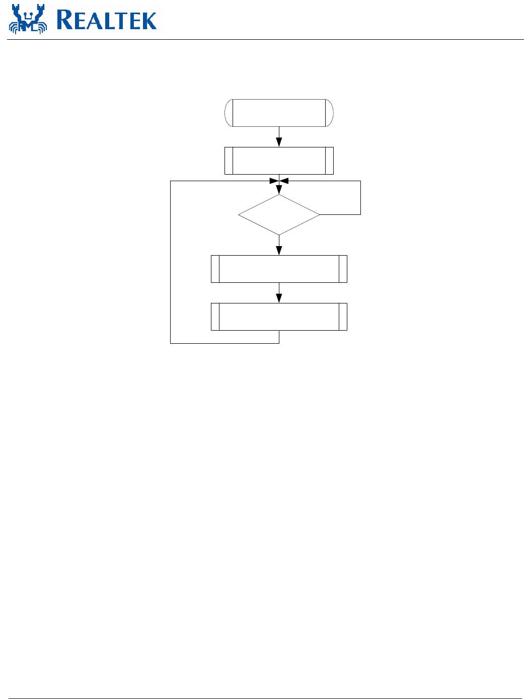
11.9.3. Rx LED
Blinking of the Rx LED indicates that receive activity is occurring.
Power On
Receiving
Packet?
LED = High
LED = High for (100 +- 10) ms
LED = Low for (12 +- 2) ms
No
Yes
Figure 3. Rx LED
RTL8187B
Datasheet
Wireless LAN Network Interface Controller 33 Track ID: JATR-1076-21 Rev. 1.0
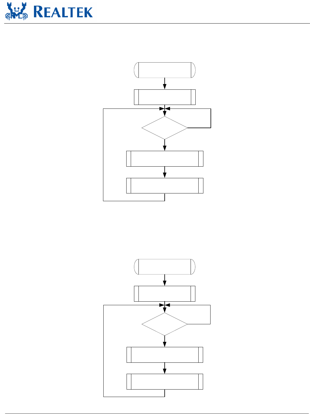
11.9.4. Tx LED
Blinking of the Tx LED indicates that transmit activity is occurring.
Power On
Transmitting
Packet?
LED = High
LED = High for (100 +- 10) ms
LED = Low for (12 +- 2) ms
No
Yes
Figure 4. Tx LED
11.9.5. Tx/Rx LED
Blinking of the Tx/Rx LED indicates that both transmit and receive activity is occurring.
Power On
Tx/Rx Packet?
LED = High
LED = High for (100 +- 10) ms
LED = Low for (12 +- 2) ms
No
Yes
Figure 5. Tx/Rx LED
RTL8187B
Datasheet
Wireless LAN Network Interface Controller 34 Track ID: JATR-1076-21 Rev. 1.0
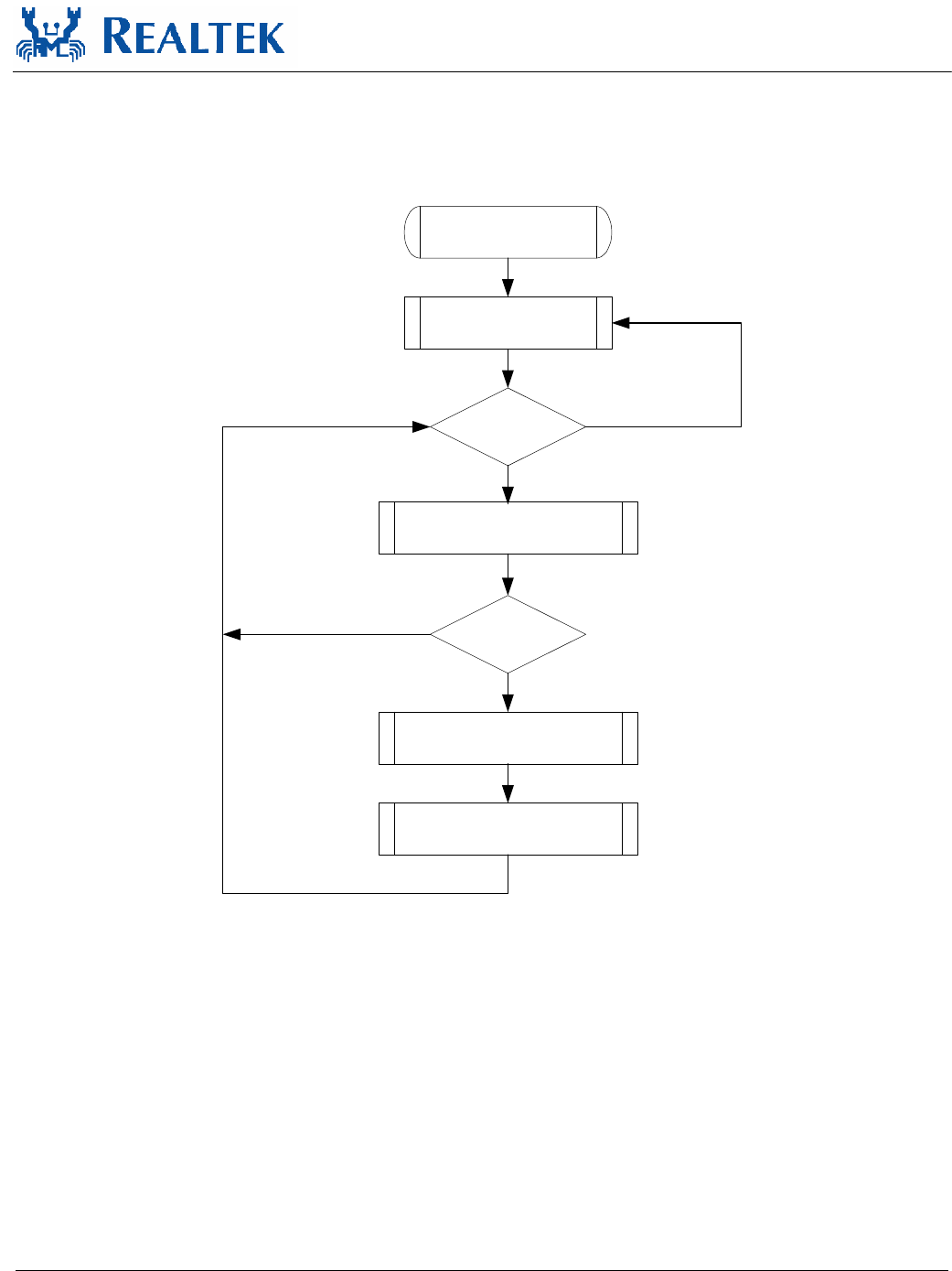
11.9.6. LINK/ACT LED
Blinking of the LINK/ACT LED indicates that the RTL8187B is linked and operating properly. If this LED
is high for extended periods it indicates that a link problem exists.
Power On
Link?
LED = High
LED = Low
LED = Low for (12 +- 2) ms
No
Yes
Tx/Rx packet?
Yes
No
LED = High for (100 +- 10) ms
Figure 6. LINK/ACT LED
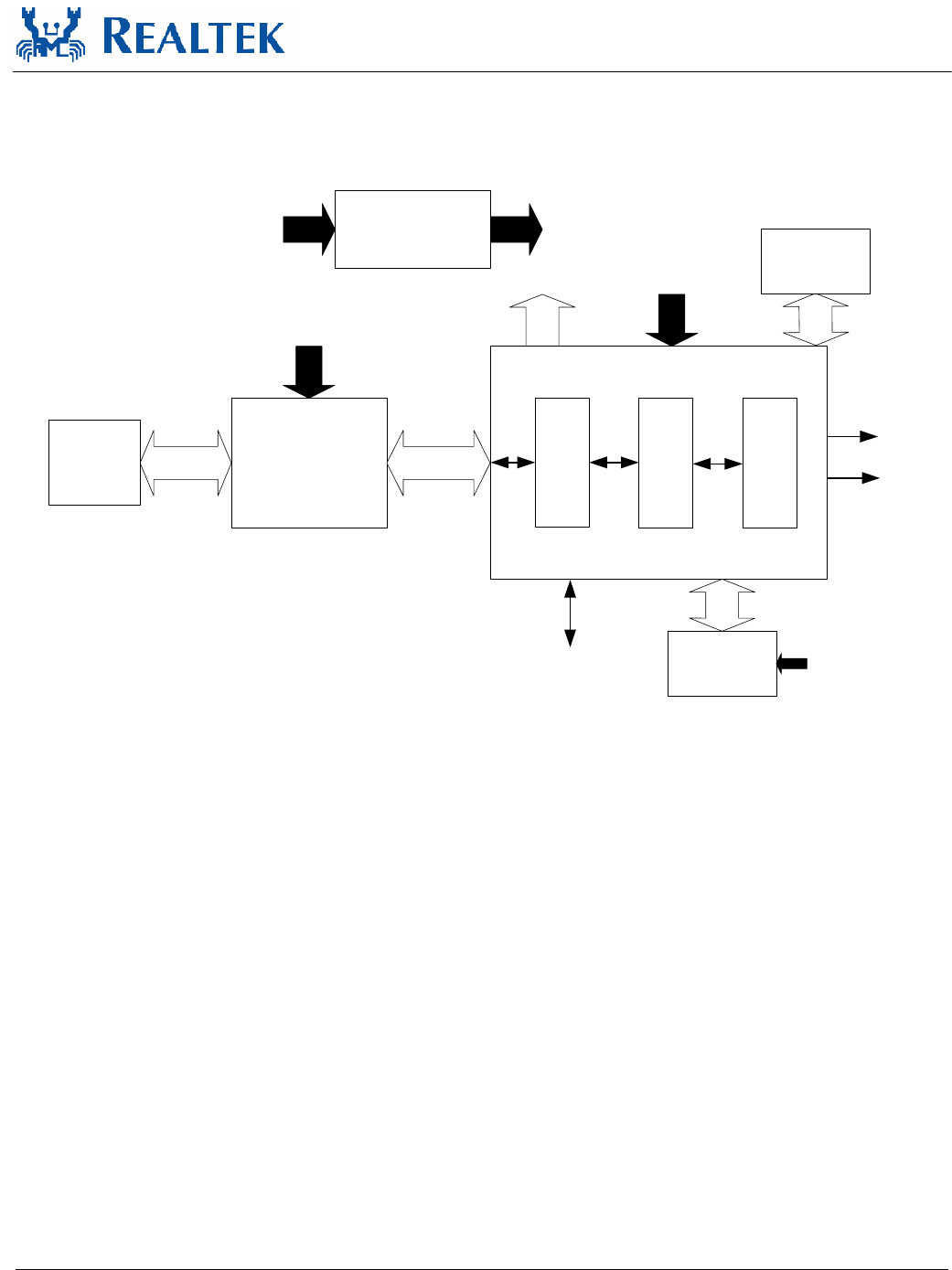
RTL8187B
Datasheet
Wireless LAN Network Interface Controller 35 Track ID: JATR-1076-21 Rev. 1.0
12. Application Diagram
RTL8187B
LED
Regulators
Main/Aux. Power Power 3.3V, 1.5V
Power 3.3V, 1.5V
External
ROM/RAM
D-
D+
40MHz
Clock
EEPROM Power 3.3V
SIEMAC
Base
Band
Power 3.3V, 1.8V
External
RF
Devices
Antenna
Figure 7. Application Diagram
RTL8187B
Datasheet
Wireless LAN Network Interface Controller 36 Track ID: JATR-1076-21 Rev. 1.0
13. Electrical Characteristics
13.1.
Temperature Limit Ratings
Table 33. Temperature Limit Ratings
Parameter Minimum Maximum Units
Storage temperature -55 +125 °C
Operating temperature -10 70 °C
13.2.
DC Characteristics
Table 34. DC Characteristics
Symbol Parameter Conditions Minimum Typical Maximum Units
VDD33 3.3V Supply Voltage 3.0 3.3 3.6 V
VDD15 1.5V Supply Voltage 1.4 1.5 1.6 V
Voh Minimum High Level Output
Voltage
Ioh = -8mA 0.9 * Vcc Vcc V
Vol Maximum Low Level Output
Voltage
Iol = 8mA 0.1 * Vcc V
Vih Minimum High Level Input Voltage 0.5 * Vcc Vcc+0.5 V
Vil Maximum Low Level Input Voltage -0.5 0.3 * Vcc V
Iin Input Current Vin =Vcc or GND -1.0 1.0 µA
Ioz Tri-State Output Leakage Current Vout =Vcc or GND -10 10 µA
Icc Average Operating Supply Current Iout = 0mA 242 mA
RTL8187B
Datasheet
Wireless LAN Network Interface Controller 37 Track ID: JATR-1076-21 Rev. 1.0
13.3.
AC Characteristics
13.3.1. Serial EEPROM Interface Timing (93C46(64*16)/93C56(128*16))
EESK
EECS
EEDI
EEDO
110An A2 A0A1
Dn D1 D0
EESK
(Read)
(Write)
(Read)
(Write)
0
tcs
EESK
EECS
EEDI
EEDO
110AnA0
...
Dn
tcs
... D0
BUSY READY
High Impedance
High Impedance
twp
EECS
EEDI
EEDO
EEDO
(Read)
(Program) STATUS VALID
tsk
tskh tskl
tcss
tdis tdih
tdos tdoh
tcsh
tsv
Figure 8. Serial EEPROM Interface Timing
Table 35. EEPROM Access Timing Parameters
Symbol Parameter Minimum Typical Maximum Units
tcs Minimum CS Low Time 9346/9356 1000/250 ns
twp Write Cycle Time 9346/9356 10/10 ms
tsk SK Clock Cycle Time 9346/9356 4/1 µs
tskh SK High Time 9346/9356 1000/500 ns
tskl SK Low Time 9346/9356 1000/250 ns
tcss CS Setup Time 9346/9356 200/50 ns
tcsh CS Hold Time 9346/9356 0/0 ns
tdis DI Setup Time 9346/9356 400/50 ns
tdih DI Hold Time 9346/9356 400/100 ns
tdos DO Setup Time 9346/9356 2000/500 ns
tdoh DO Hold Time 9346/9356 2000/500 ns
tsv CS to Status Valid 9346/9356 1000/500 ns
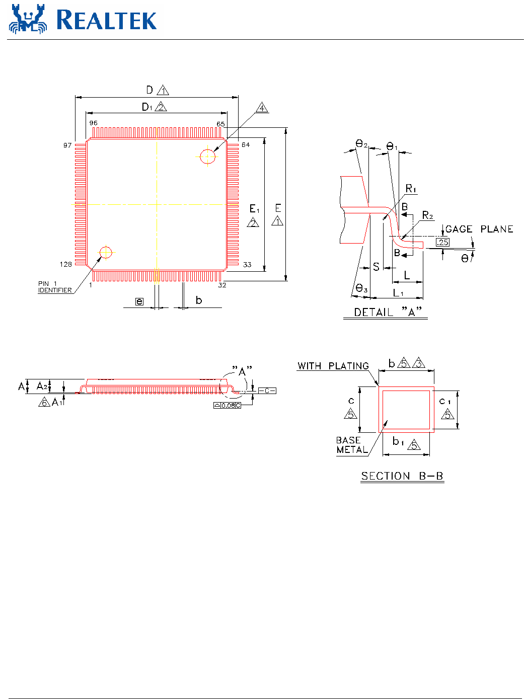
RTL8187B
Datasheet
Wireless LAN Network Interface Controller 38 Track ID: JATR-1076-21 Rev. 1.0
14. Mechanical Dimensions
See the Mechanical Dimensions notes on the next page.
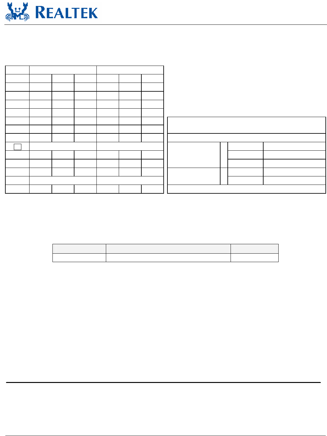
RTL8187B
Datasheet
Wireless LAN Network Interface Controller 39 Track ID: JATR-1076-21 Rev. 1.0
14.1.
Mechanical Dimensions Notes
Note:
Symbol Dimension in inch Dimension in mm 1.Dimension b does not include dambar
Min Typical Max Min Typical Max
protrusion/intrusion.
A - - 0.063 - - 1.60
2.Controlling dimension: Millimeter
A1 0.002 - - 0.05 - -
3.General appearance spec. should be based
A2 0.053 0.055 0.057 1.35 1.40 1.45 on final visual inspection spec.
b 0.005 0.007 0.009 0.13 0.18 0.23
c 0.004 - 0.006 0.09 - 0.20
TITLE: 128LD LQFP ( 14x14x1.4 mm*2 ) PACKAGE OUTLINE
D 0.624 0.630 0.636 15.85 16.00 16.15 -CU L/F, FOOTPRINT 2.0 mm
D1 0.547 0.551 0.555 13.90 14.00 14.10 LEADFRAME MATERIAL:
e 0.016 BSC 0.40 BSC APPROVE DOC. NO. 530-ASS-P004
E 0.624 0.630 0.636 15.85 16.00 16.15 VERSION 1
E1 0.547 0.551 0.555 13.90 14.00 14.10 PAGE OF
L 0.018 0.024 0.030 0.45 0.60 0.75 CHECK DWG NO. LQ128 - 2
L1 0.039 REF 1.00 REF DATE MAY. 13.2002
Θ 0° 3.5° 7° 0° 3.5° 7°
REALTEK SEMICONDUCTOR CORP.
15. Ordering Information
Table 36. Ordering Information
Part Number Package Status
RTL8187B-GR 128-pin LQFP with green package MP
Note: See page 5 for Green package identification.
Realtek Semiconductor Corp.
Headquarters
No. 2, Innovation Road II, Hsinchu Science Park,
Hsinchu 300, Taiwan.
Tel: 886-3-5780211 Fax: 886-3-5776047
www.realtek.com.tw

The content of this PDF file is in accordance with the original issued reports for reference only. This Test Report cannot be reproduced, except in full,
without prior written permission of the Company
SGS TAIWAN LIMITED NO. 136-1, Wu Kung Road, WuKu Industrial Zone, Taipei county, Taiwan.
t(886-2) 22993939 f(886-2) 2299-3237 www.sgs.com.tw
Test Report
Report No. : CE/2005/12075
Date : 2005/01/20
Page : 1 of 2
Type of Product :
Style/Item No :
Sample Received :
Testing Date :
===========================================================================
=
Test Result :- Please see the next page -
REALTEK SEMICONDUCTOR CORP.
NO. 2, INDUSTRY E. RD. IX, SCIENCE-BASED INDUSTRIAL
PARK, HSINCHU 300, TAIWAN
The following merchandise was (were) submitted and identified by the client as :
LQFP (LF)
4C055S2
2005/01/13
2005/01/13 TO 2005/01/20

The content of this PDF file is in accordance with the original issued reports for reference only. This Test Report cannot be reproduced, except in full,
without prior written permission of the Company
SGS TAIWAN LIMITED NO. 136-1, Wu Kung Road, WuKu Industrial Zone, Taipei county, Taiwan.
t(886-2) 22993939 f(886-2) 2299-3237 www.sgs.com.tw
Test Report
Report No. : CE/2005/12075
Date : 2005/01/20
Page : 2 of 2
Test Result
PART NAME NO.1 :
Result
No.1
PBBs(Polybrominated
biphenyls)(CAS NO:059536-
65-1)
% With reference to
USEPA3540 or USEPA3550.
Analysis was performed by
HPLC/DAD, LC/MS or
GC/MS. (prohibited by
2002/95/EC (RoHS),
83/264/EEC, and
76
/
769
/
EEC
)
0.0005 N.D.
PBBEs(PBDEs)(Polybrominat
ed biphenyl ethers)
% With reference to
USEPA3540 or USEPA3550.
Analysis was performed by
HPLC/DAD, LC/MS or
GC/MS. (prohibited by
2002/95/EC (RoHS),
83/264/EEC, and
76
/
769
/
EEC
)
0.0005 N.D.
Result
No.1
Chromium VI (Cr+6) ppm As per US EPA 7196A and
US EPA 3060A.
2 N.D.
Cadmium (Cd) ppm ICP-AES after as per EN
1122, method B:2001 or
other acid digestion.
2 N.D.
Mercury (Hg) ppm ICP-AES after as per US
EPA 3052 or other acid
digestion.
2 N.D.
Lead (Pb) ppm ICP-AES after as per US
EPA 3050B or other acid
digestion.
2 N.D.
MIXED BLACK PLASTIC BODY&SILVER COLORED
METAL-MIXED ALL PART
Test Item (s): Method MDLUnit
NOTE: (1) N.D. = Not detected (<MDL)
(2) ppm = mg/kg
(3) MDL = Method Detection Limit
REALTEK SEMICONDUCTOR CORP.
NO. 2, INDUSTRY E. RD. IX, SCIENCE-BASED INDUSTRIAL
PARK, HSINCHU 300, TAIWAN
Test Item (s): Unit Method MDL
Federal Communication Commission Interference
Statement
This equipment has been tested and found to comply with the limits for a Class B
digital device, pursuant to Part 15 of the FCC Rules. These limits are designed to
provide reasonable protection against harmful interference in a residential installation.
This equipment generates, uses and can radiate radio frequency energy and, if not
installed and used in accordance with the instructions, may cause harmful interference
to radio communications. However, there is no guarantee that interference will not
occur in a particular installation. If this equipment does cause harmful interference
to radio or television reception, which can be determined by turning the equipment off
and on, the user is encouraged to try to correct the interference by one of the
following measures:
Reorient or relocate the receiving antenna.
Increase the separation between the equipment and receiver.
Connect the equipment into an outlet on a circuit different from that to which
the receiver is connected.
Consult the dealer or an experienced radio/TV technician for help.
FCC Caution: Any changes or modifications not expressly approved by the party
responsible for compliance could void the user's authority to operate this equipment.
This device complies with Part 15 of the FCC Rules. Operation is subject to the
following two conditions: (1) This device may not cause harmful interference, and (2)
this device must accept any interference received, including interference that may
cause undesired operation.
This device and its antenna(s) must not be co-located or operating in conjunction with
any other antenna or transmitter.
IMPORTANT NOTE:
This module is intended for OEM integrator. The OEM integrator is still responsible
for the FCC compliance requirement of the end prouduct which integrates this
module.
20cm minimum distance has to be able to be maintained between the antenna and
the users for the host this module is integrated into. Under such configuration, the
FCC radiation exposure limits set forth for an population/uncontrolled environment
can be satisfied.
Any changes or modifications not expressly approved by the manufacturer
could void the user's authority to operate this equipment.
USERS MANUAL OF THE END PRODUCT:
In the users manual of the end product, the end user has to be informed to keep
at least 20cm separation with the antenna while this end product is installed and
operated. The end user has to be informed that the FCC radio-frequency
exposure guidelines for an uncontrolled environment can be satisfied. The end
user has to also be informed that any changes or modifications not expressly
approved by the manufacturer could void the user's authority to operate this
equipment. If the size of the end product is smaller than 8x10cm, then additional
FCC part 15.19 statement is required to be available in the users manual: This
device complies with Part 15 of FCC rules. Operation
is subject to the following two conditions: (1) this device may not cause harmful
interference and (2) this device must accept any interference received, including
interference that may cause undesired operation.
LABEL OF THE END PRODUCT:
The final end product must be labeled in a visible area with the following
" Contains TX FCC ID: TX2-RTL8187B ". If the size of the end product is larger than
8x10cm, then the following FCC part 15.19 statement has to also
be available on the label: This device complies with Part 15 of FCC rules. Operation
is subject to the following two conditions: (1) this device may not cause harmful
interference and (2) this device must accept any interference received, including
interference that may cause undesired operation.
IC Radiation Exposure Statement:
"Operation is subject to the following two conditions: (1) this device may not cause
interference, and (2) this device must accept any interference, including interference that
may cause undesired operation of the device."
Without Co-located
The antenna (s) used for this transmitter must not be co-located or operating in conjunction with any other
antenna or transmitter.
For product available in the USA/Canada market, only channel 1~11 can be operated.
Selection of other channels is not possible.
Modular OEM Integrator Notice
End Product Labeling
This transmitter module is authorized only for use in device where the antenna may be installed such
that 20 cm may be maintained between the antenna and users. The final end product must be labeled
in a visible area with the following: "Contains TX IC: 6317A-RTL8187B"