Realtek Semiconductor RTL8187SE 802.11b/g RTL8187SE miniCard User Manual xRTL8187SE DataSheet 1 0 11 DRAFT
Realtek Semiconductor Corp. 802.11b/g RTL8187SE miniCard xRTL8187SE DataSheet 1 0 11 DRAFT
Contents
- 1. User Manual
- 2. User Manual for the host
User Manual
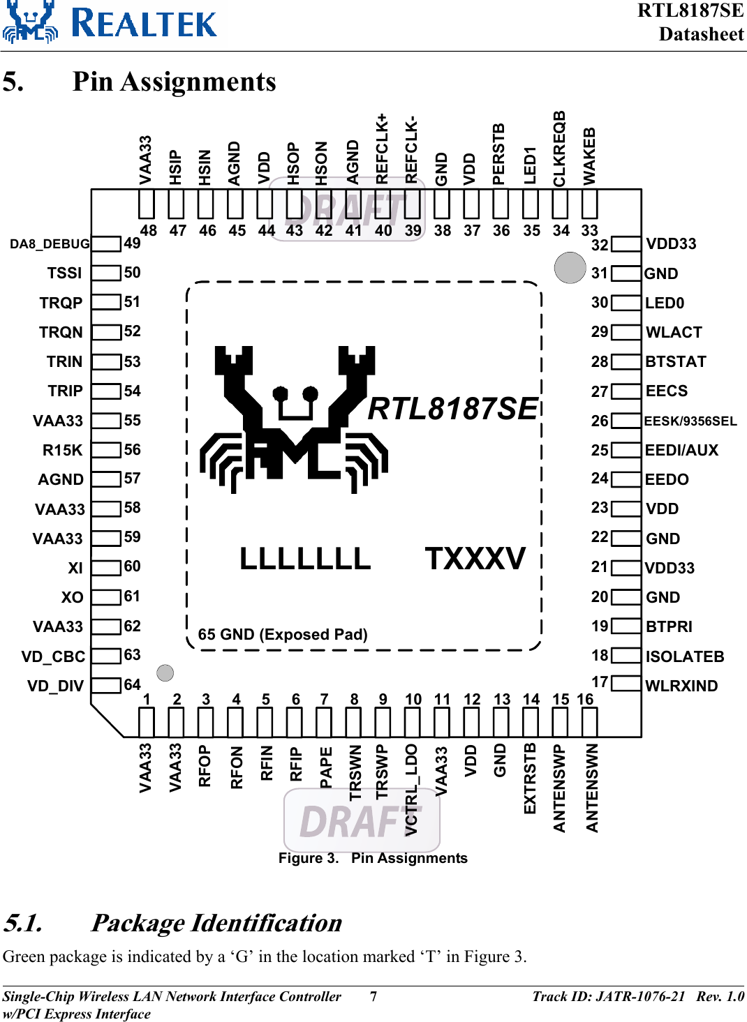
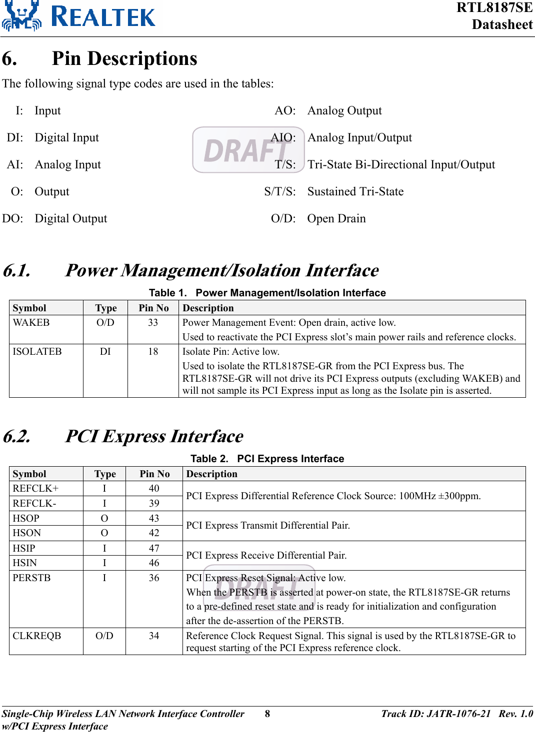
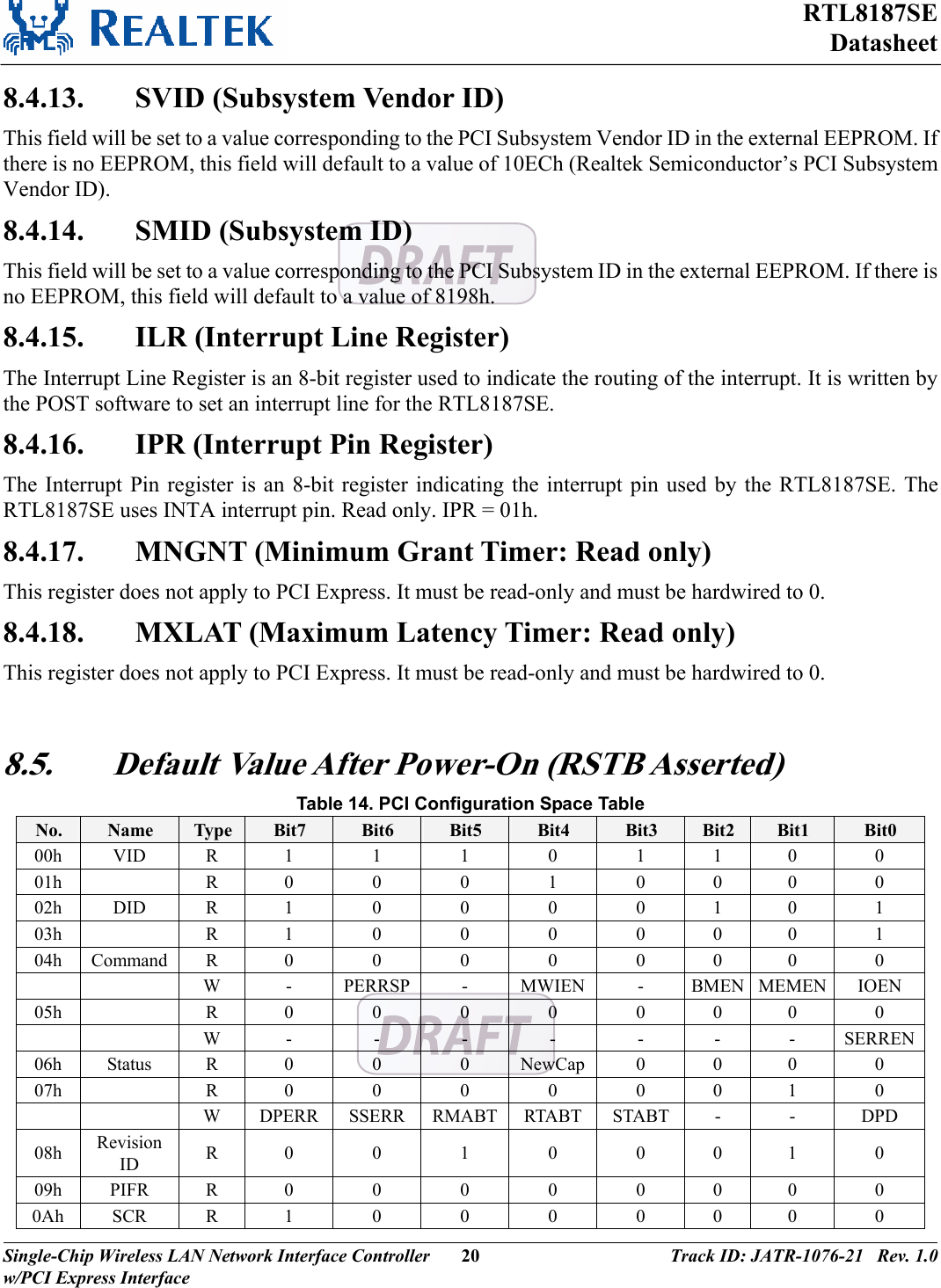
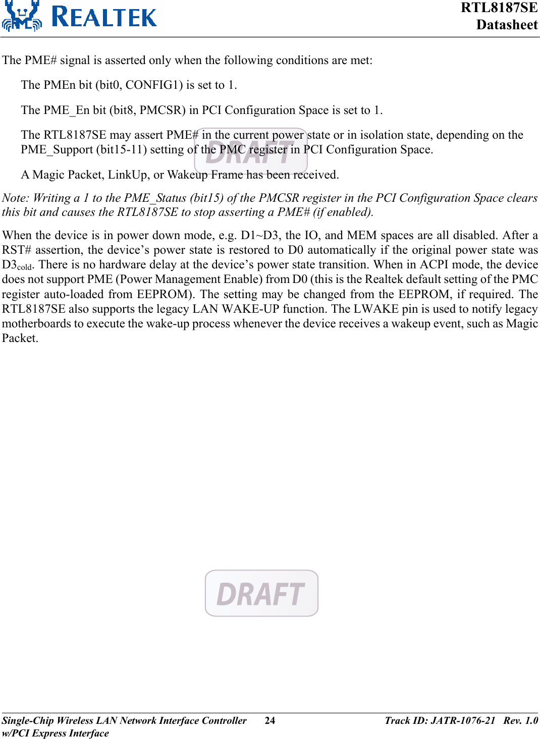
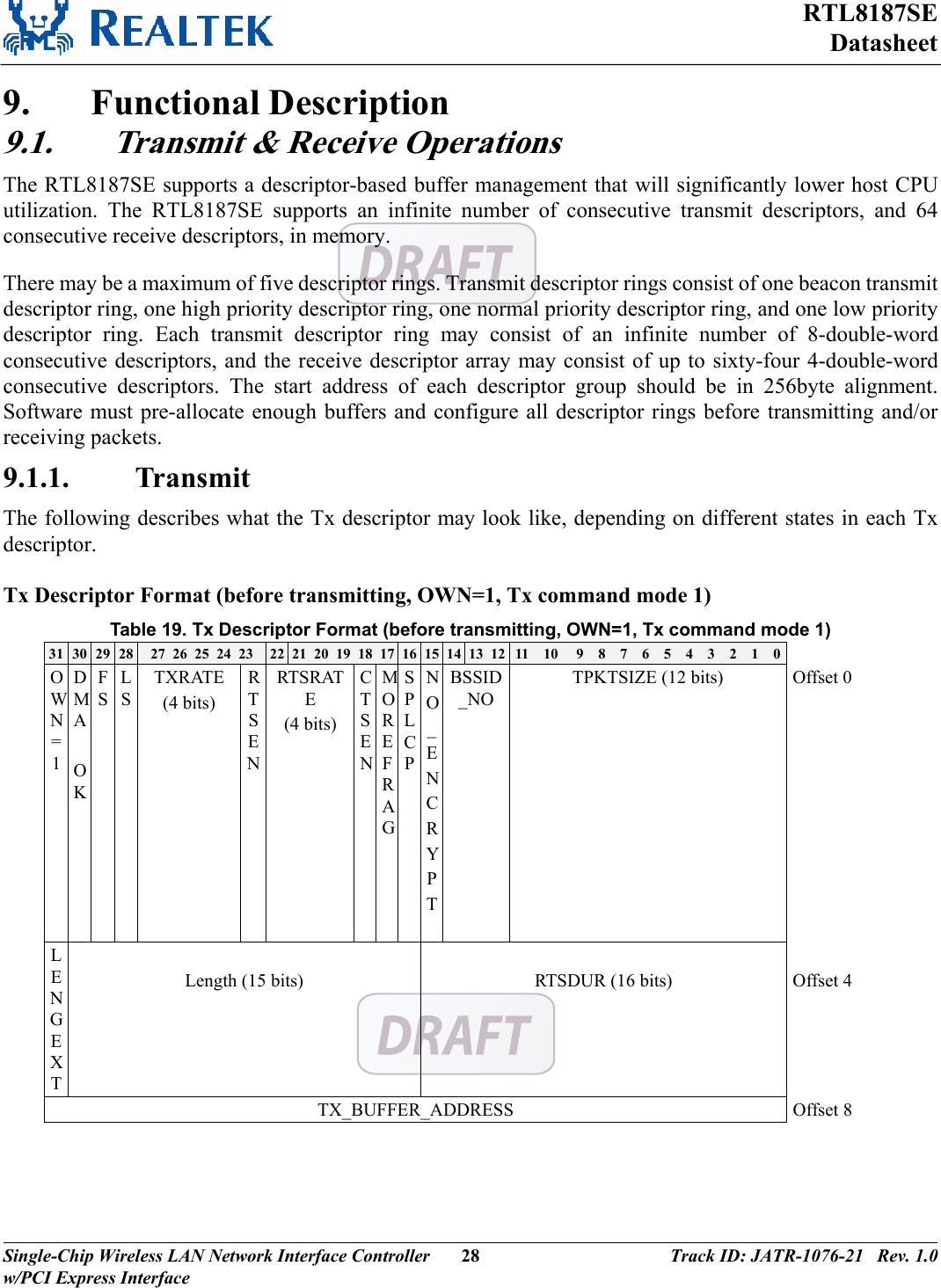
![RTL8187SEDatasheetSingle-Chip Wireless LAN Network Interface Controller w/PCI Express Interface 9Track ID: JATR-1076-21 Rev. 1.06.3. EEPROM Interface Table 3. EEPROM Interface Symbol Type Pin No DescriptionEESK/9356SEL DO/DI 26 EESK in 93C46 (93C56) programming or auto-load mode. Input Pin as 9356 Select Pin at Initial Power-up. When this pin is pulled high with a 10K resistor, the 93C56 EEPROM is used to store the resource data for the RTL8187SE. The RTL8187SE latches the status of this pin at power-up to determine which EEPROM (93C46 or 93C56) is used. After power on and GPIO_EN[5]=1, this pin is GPIO[5]. EEDI/AUX DO/DI 25 EEDI: Output to serial data input pin of EEPROM. AUX: Input pin to detect if Aux. Power exists or not on initial power-on. This pin should be connected to EEPROM. To support wakeup from ACPI D3cold or APM power-down, this pin must be pulled high to Aux. Power via a resistor. If this pin is not pulled high to Aux. Power, the RTL8187SE assumes that no Aux. Power exists. After power on and GPIO_EN[4]=1, this pin is GPIO[4]. EEDO DI 24 This pin is GPIO[3] after power on and GPIO_EN[3]=1, otherwise, it is EEDO in 93C46 (93C56) programming or auto-load mode. EECS DO 27 EEPROM Chip Select. 93C46 (93C56) chip select. 6.4. Power Pins Table 4. Power Pins Symbol Type Pin No DescriptionVDD33 P 21, 32 +3.3V (Digital). VAA33 P 1, 2, 11, 48, 55, 58, 59, 62+3.3V (Analog). VDD P 12, 23, 37, 44 +1.8V. GND P 13, 20, 22, 31, 38, 65 Ground (Digital). AGND P 41, 45, 57 Ground (Analog). VCTRL_LDO AO 10 Reserve this pin for external BJT option to generate 1.8V for digital core circuit. VD_CBC P 63 Reserved for external power transistor. VD_DIV P 64 Reserved for external power transistor.](https://usermanual.wiki/Realtek-Semiconductor/RTL8187SE.User-Manual/User-Guide-903053-Page-15.png)
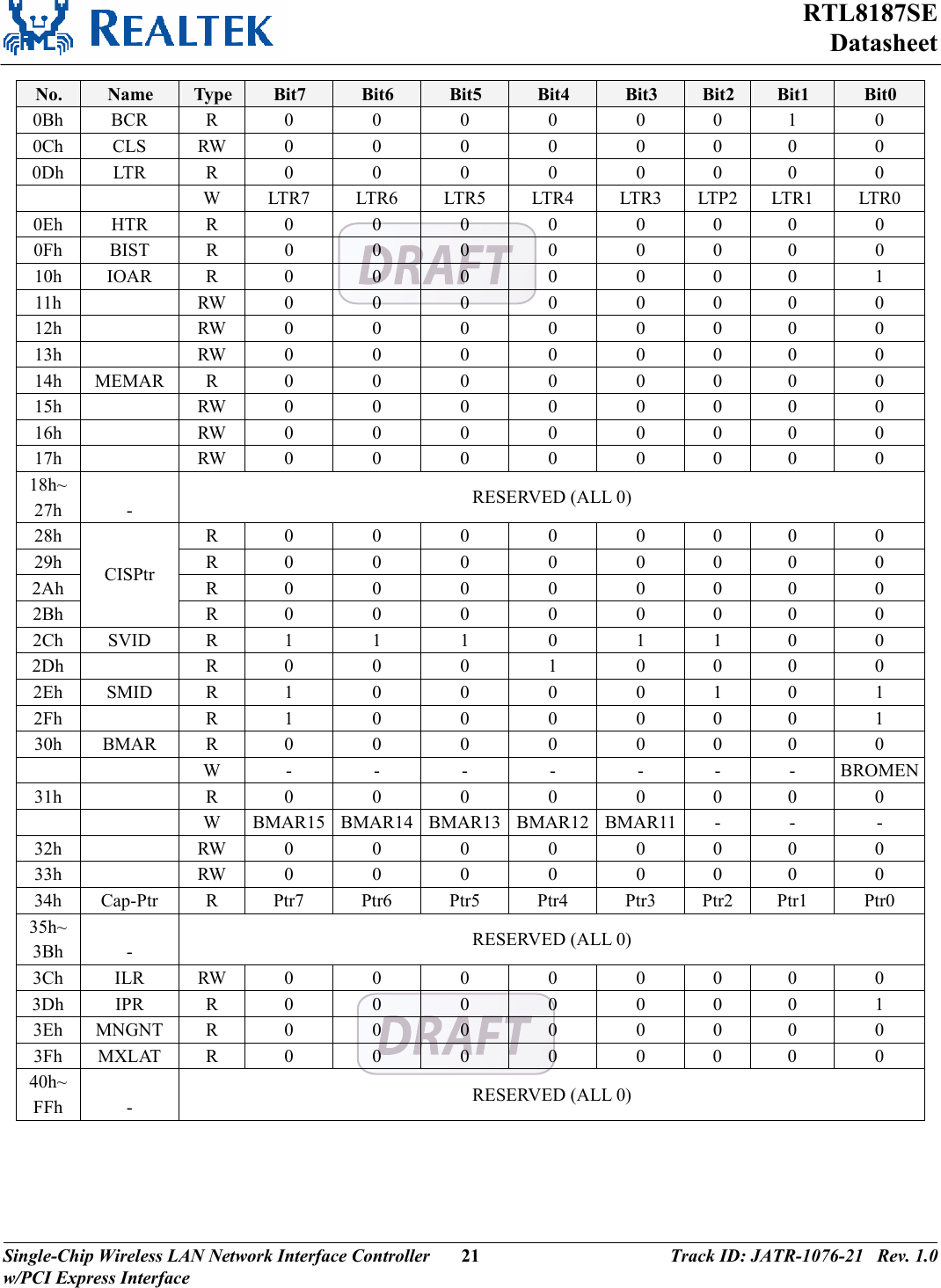
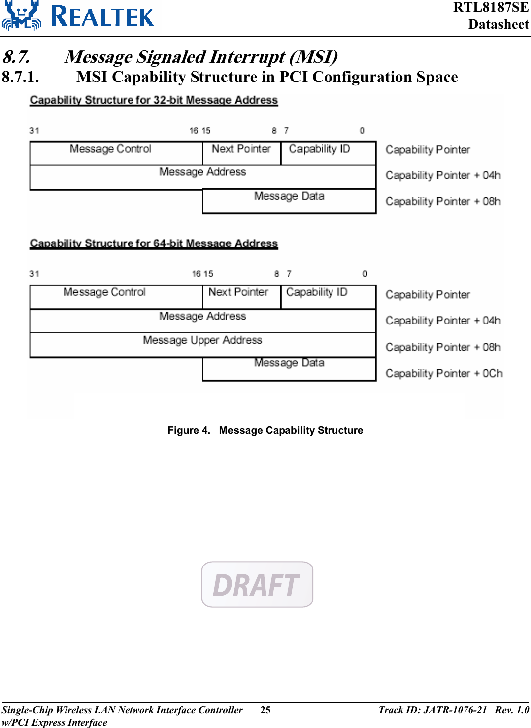
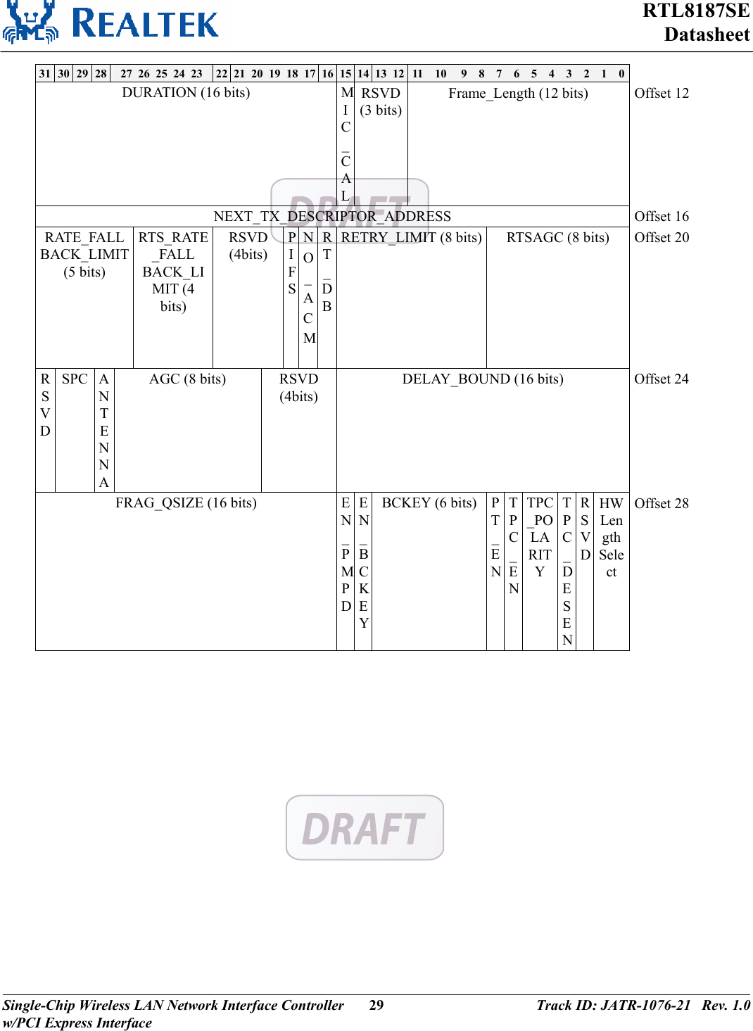
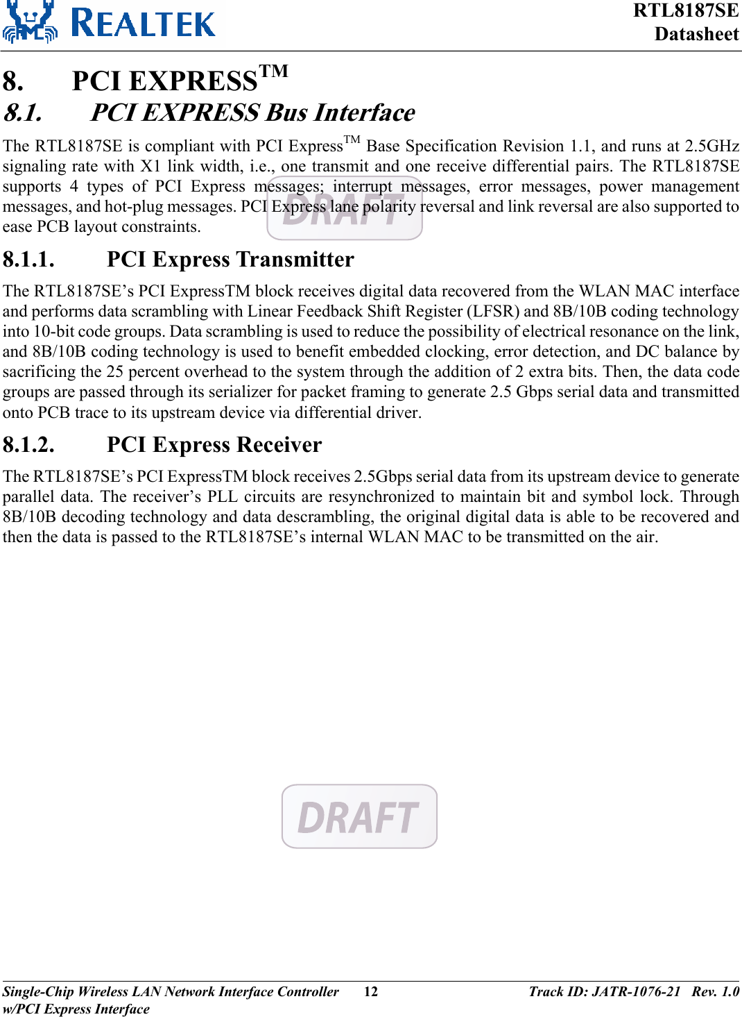
![RTL8187SEDatasheetSingle-Chip Wireless LAN Network Interface Controller w/PCI Express Interface 10 Track ID: JATR-1076-21 Rev. 1.06.5. LED Interface Table 5. LED Interface Symbol Type Pin No DescriptionLED0 O 30 LED Pin. a. PWRON: I2C_CK b. After PWRON & LED_CONTROL=3’h7: GPIO[0] c. Other: LED0 LED1 O 35 LED Pin. a. PWRON: I2C_IO b. After PWRON & LED_CONTROL=3’h7: GPIO[1] c. Other: LED1 6.6. Baseband and RF Pins Table 6. Baseband and RF Pins Symbol Type Pin No DescriptionRFOP AO 3 RFON AO 4 2.4GHz Differential RF Power Amplifier Output. RFIN AI 5 RFIP AI 6 2.4GHz Differential RF Input. PAPE DO 7 Enable Control for Optional External Power Amplifier TRSWN DO 8 TRSWP DO 9 Control Signals for Optional External RF T/R Switch ANTENSWP DO 15 ANTENSWN DO 16 Control Signals for Antenna Switch TSSI AI 50 Transmit Signal Strength Indication From External Power Amplifier TRQP AIO 51 Via register setting, can be programmed to one of the following four types of pins:RF TXQP: Input pin for RF TX test RF RXQP: Output pin for RF RX test AFE TXQP: Output pin for DAC test AFE RXQP: Input pin for ADC test TRQN AIO 52 Via register setting, can be programmed to one of the following four types of pins:RF TXQN: Input pin for RF TX test RF RXQN: Output pin for RF RX test AFE TXQN: Output pin for DAC test AFE RXQN: Input pin for ADC test TRIN AIO 53 Via register setting, can be programmed to one of the following four types of pins:RF TXIN: Input pin for RF TX test RF RXIN: Output pin for RF RX test AFE TXIN: Output pin for DAC test AFE RXIN: Input pin for ADC test TRIP AIO 54 Via register setting, can be programmed to one of the following four types of pins:RF TXIP: Input pin for RF TX test RF RXIP: Output pin for RF RX test AFE TXIP: Output pin for DAC test AFE RXIP: Input pin for ADC test](https://usermanual.wiki/Realtek-Semiconductor/RTL8187SE.User-Manual/User-Guide-903053-Page-16.png)
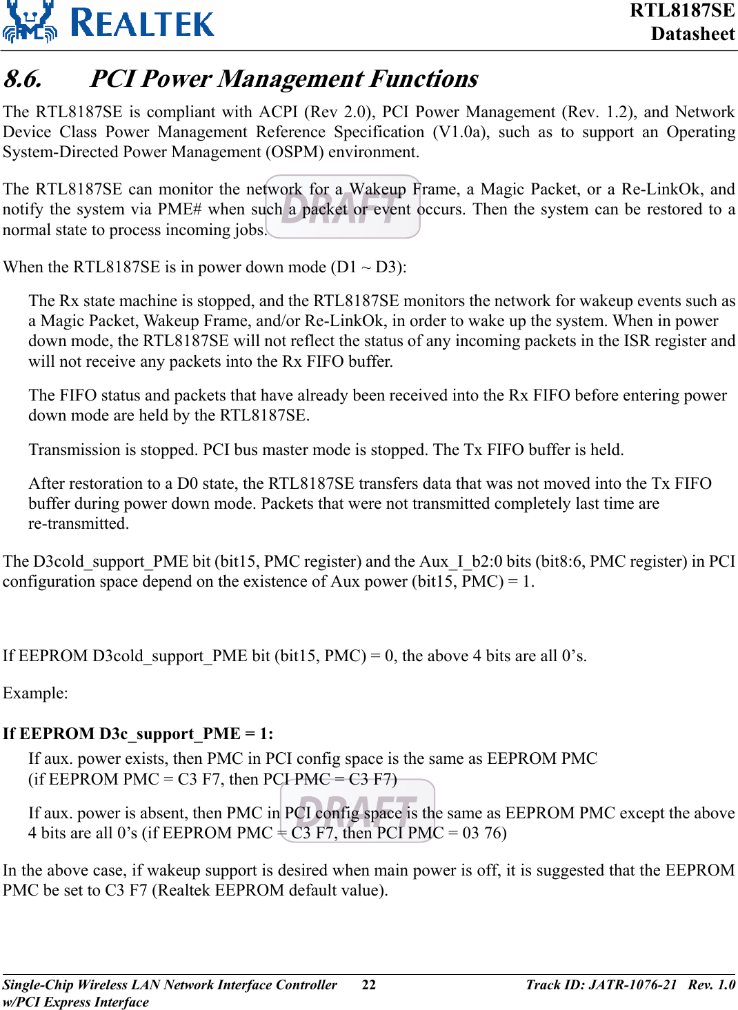
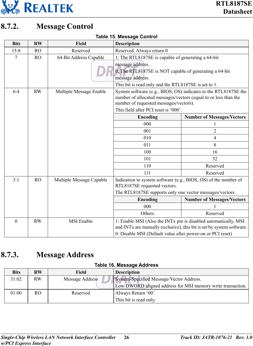
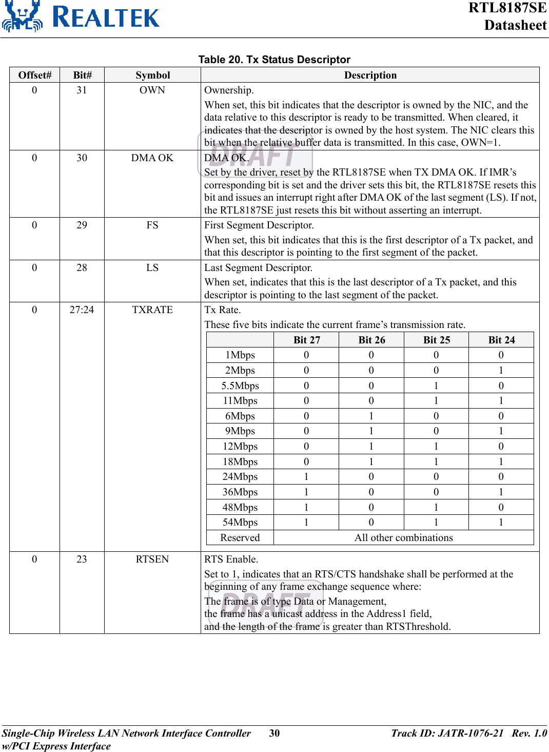
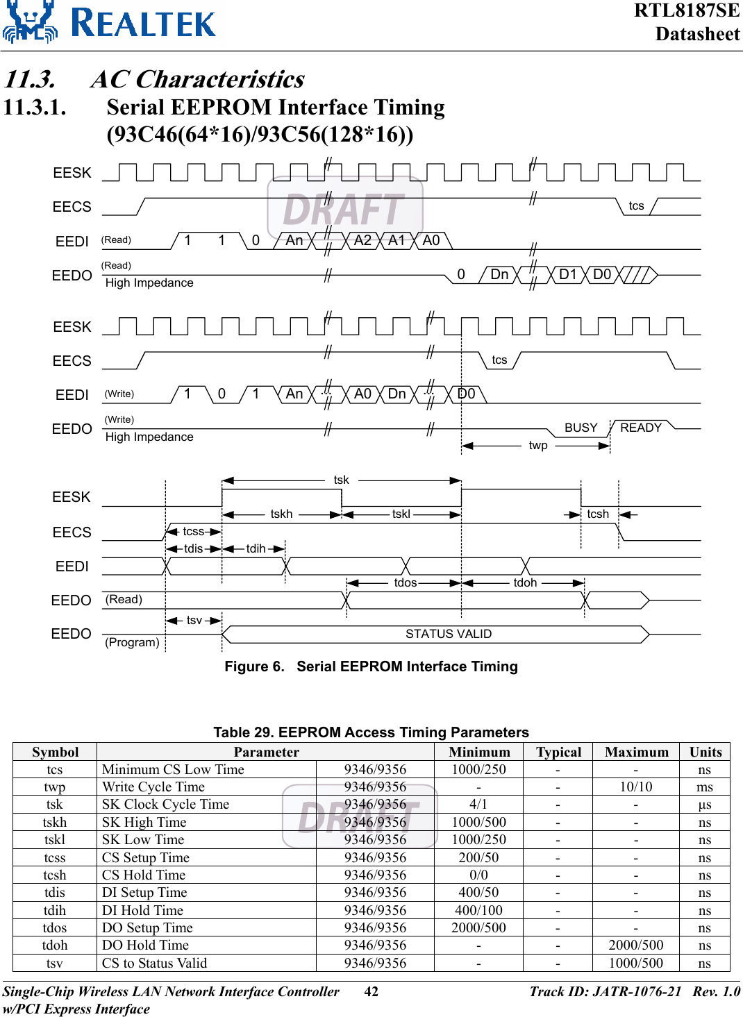
![RTL8187SEDatasheetSingle-Chip Wireless LAN Network Interface Controller w/PCI Express Interface 11 Track ID: JATR-1076-21 Rev. 1.06.7. Bluetooth Co-Existence Pins Table 7. Bluetooth Co-Existence Pins Symbol Type Pin No DescriptionWLRXIND O 17 Wireless LAN RX Activity Indicator BTPRI IO 19 Bluetooth Priority Pin This pin is GPIO[2] after power on and GPIO_EN[2]=1, otherwise, this pin is BTPRI. The BTPRI signal indicates when an important Bluetooth packet is being transmitted or received. BTSTAT IO 28 Bluetooth Status This pin is GPIO[6] after power on and GPIO_EN[6]=1, otherwise, this pin is BTSTAT. The BTSTAT signal indicates when normal Bluetooth packets are being transmitted or received. WLACT O 29 WLAN Activity The WLAN_Active signal indicates when WLAN is either transmitting or receiving in the 2.4GHz ISM band. 6.8. Clock and Other Pins Table 8. Clock and Other Pins Symbol Type Pin No DescriptionR15K IO 56 This pin must be pulled low by a 15K resistor. XI I 60 Input of 40MHz Clock Reference. XO O 61 Output of 40MHz Clock Reference. EXTRSTB I 14 External Reset Pin: Active Low. DA8_DEBUG O 49 Debug Pin. 7. EEPROM (93C46 or 93C56) Contents The RTL8187SE supports the attachment of an external EEPROM. The 93C46 is a 1Kbit EEPROM (the 93C56 is a 2Kbit EEPROM). The EEPROM interface provides the ability for the RTL8187SE to read from, and write data to, an external serial EEPROM device. Values in the external EEPROM allow default fields in PCI configuration space and IO space to be overridden following an internal power on reset, or software EEPROM auto-load command. The RTL8187SE will auto-load values from the EEPROM to these fields in configuration space and IO space. If the EEPROM is not present, the RTL8187SE initialization uses default values for the appropriate Configuration and Operational Registers. Software can read and write to the EEPROM using ‘bit-bang’ accesses via the 9346CR Register. Note: It is suggested to obtain Realtek approval before changing the default settings of the EEPROM.](https://usermanual.wiki/Realtek-Semiconductor/RTL8187SE.User-Manual/User-Guide-903053-Page-17.png)
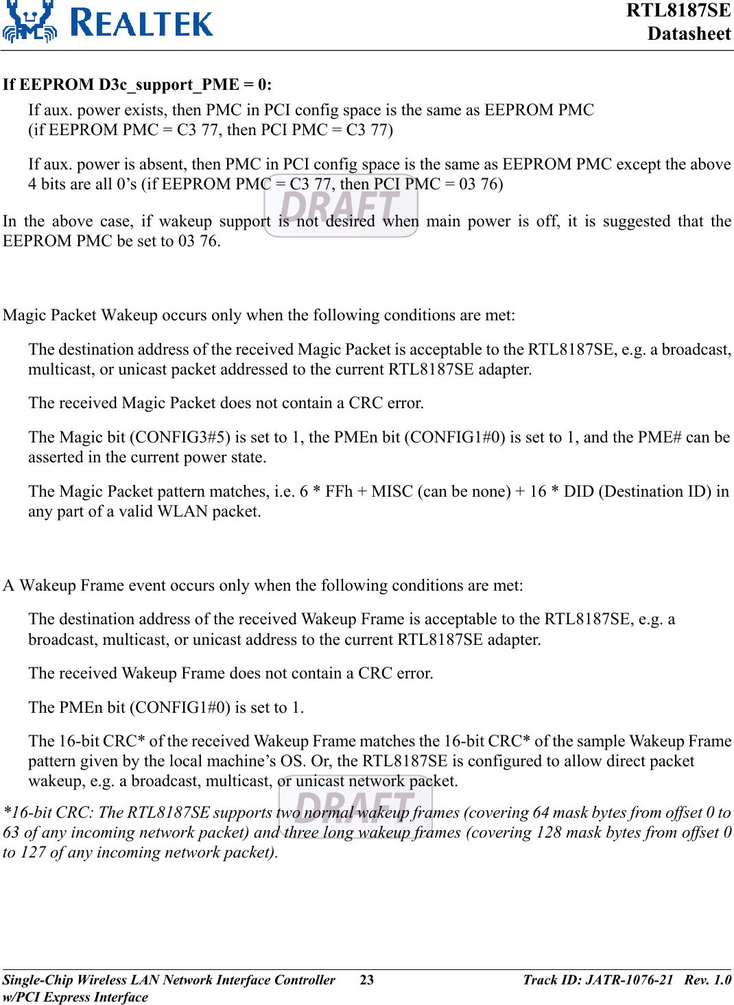
![RTL8187SEDatasheetSingle-Chip Wireless LAN Network Interface Controller w/PCI Express Interface 14 Track ID: JATR-1076-21 Rev. 1.0No. Name Type Bit7 Bit6 Bit5 Bit4 Bit3 Bit2 Bit1 Bit03Fh MXLAT R 0 0 0 0 0 0 0 0 40h PMID R 0 0 0 0 0 0 0 1 41h NextPtr R 0 1 0 1 0 0 0 0 42h R Aux_I_b1 Aux_I_b0 DSI Reserved PMECLK Version 43hPMCR PME_D3cold PME_D3hot PME_D2 PME_D1 PME_D0 D2 D1 Aux_I_b2R 0 0 0 0 0 0 Power State 44hW - - - - - - Power State R PME_Status - - - - - - PME_En45hPMCSRW PME_Status - - - - - - PME_En46- 4FhReserved50h MSIID R 0 0 0 0 0 1 0 1 51h NextPtr R 0 1 1 1 0 0 0 0 R 64-bit Address CapableMultiple Message Enable 0 0 0 MSI Enable52hW - Multiple Message Enable - - 0 MSI Enable53hMessageControl Reserved. Always return 0 54h- 57hMessageAddress Low RW 64-bit Interrupt Message Address Low 58h- 5BhMessageAddress High RW 64-bit Interrupt Message Address High 5Ch- 5DhMessage Data RW 16-bit Message Data 5E- 6FhRESERVED 70h PCIEID R 0 0 0 1 0 0 0 0 71h NextPtr R 0 0 0 0 0 0 0 0 R 0 0 0 Legacy 0 0 0 1 72h- 73hPCIE Cap. R 0 0 0 0 0 0 0 0 R L0s_acpt_ latency[1]L0s_acpt_latency[0]Entend_ tag_support0 0 Max_payload_size_support R Role Base Error rpt 0 0 0 L1_acpt_ latency[2]L1_acpt_latency[1]L1_acpt_latency[0]L0s_acpt_latency[2] R 0 0 0 0 0 0 0 0 74h- 77hDeviceCapabilityRegisterR 0 0 0 0 0 0 0 0 RW Max_payload_size Relaxed_ ordering_enUnsupport_rqst_rpt_enFatal_err_rpt_en Non_fatal_err_rpt_enCorrect- able_err_rpt_en 78h- 79hDeviceControl RegisterRW 0 Max_read_request_size No_snoop_en Auxpwr_ PM_en 0 Entend_ tag_enR 0 0 Transact_ ion_pendingAuxPwr_det Upsupport_rqst_det Fatal_err_det Non_fatal_err_det Correct- able_err_det7AhW 0 0 - - Upsupport_rqst_det Fatal_err_det Non_fatal_err_detCorrecta-ble_err_det7BhDevice Status RegisterR 0 0 0 0 0 0 0 0 7Ch R 0 0 0 1 0 0 0 1 7Dh R L1_exit_ lat[0]L0s_exit_lat[2]L0s_exit_lat[1]L0s_exit_lat[0]ASPM_support 0 0 7Eh R 0 0 0 0 0 Clock_PM L1_exit_ lat[2]L1_exit_lat[1]07FhLink CapabilityRegisterR 0 0 0 0 0 0 0 0](https://usermanual.wiki/Realtek-Semiconductor/RTL8187SE.User-Manual/User-Guide-903053-Page-20.png)
![RTL8187SEDatasheetSingle-Chip Wireless LAN Network Interface Controller w/PCI Express Interface 15 Track ID: JATR-1076-21 Rev. 1.0No. Name Type Bit7 Bit6 Bit5 Bit4 Bit3 Bit2 Bit1 Bit0R Extended_ sync Common_ clock0 0 RCB 0 ASPM_control 80hW Extended_ sync Common_ clock0 0 RCB 0 ASPM_control R 0 0 0 0 0 0 0 Enable clock_PM81hLink Control RegisterW 0 0 0 0 0 0 0 Enable clock_PM82h R 0 0 0 1 0 0 0 1 83hLink Status Register R 0 0 0 Slot_clock_cfg 0 0 0 0 84h R Slot power Limit[0] Hot-Plug CapableHot-Plug Surprise Powerindicator presentAttn indicator presentMRL sensor presentPower controlpresentAttn button present85h R Slot power Limit scale[0] Slot power Limit[7] Slot power Limit[6] Slot power Limit[5] Slot power Limit[4] Slot power Limit[3] Slot power Limit[2] Slot power Limit[1]86h R Physical slot Number[4] Physicalslot Number[3]Physical slot Number[2]Physical slot Number[1]Physical slot Number[0]No common Complete support Electromechanical interlockpresentSlot power Limit scale[1] 87hSlotCapabilityRegisterR Physical slot Number[12] Physical slotNumber[11]Physical slot Number[1]Physical slot Number[9]Physical slot Number[8]Physical slot Number[7] Physical slot Number[6]Physical slot Number[5]88h RW Attn Indicator Control[1] Attn Indicator Control[0] Hot-Plug Interrupt Enable Command Completed interruptEnable PresenceDetectChangedEnable MRL Sensor ChangedEnable Power Fault DetectedEnable Attn Bottom PressedEnable 89hSlot Control RegisterRW - - - Data Link Layer State ChangedEnable Electromechanical Interlock Control PowerController Control PowerIndicator Control[1]PowerIndicator Control[0]8Ah R Electromechanical Interlock Status Presence Detect State MRL Sensor State Command CompletedPresenceDetectChangedMRL Sensor ChangedPower Fault DetectedAttn Botton pressed 8BhSlot Status RegisterR Reversed Data Link Layer State Changed8Ch- FFhReversed](https://usermanual.wiki/Realtek-Semiconductor/RTL8187SE.User-Manual/User-Guide-903053-Page-21.png)