Realtek Semiconductor RTL8187SE 802.11b/g RTL8187SE miniCard User Manual xRTL8187SE DataSheet 1 0 11 DRAFT
Realtek Semiconductor Corp. 802.11b/g RTL8187SE miniCard xRTL8187SE DataSheet 1 0 11 DRAFT
Contents
- 1. User Manual
- 2. User Manual for the host
User Manual

RTL8187SE
SINGLE-CHIP WIRELESS LAN NETWORK
INTERFACE CONTROLLER w/PCI EXPRESS
INTERFACE
DATASHEET
Rev. 1.0
16 January 2008
Track ID: JATR-1076-21
Realtek Semiconductor Corp.
No. 2, Innovation Road II, Hsinchu Science Park, Hsinchu 300, Taiwan
Tel.: +886-3-578-0211. Fax: +886-3-577-6047
www.realtek.com.tw

RTL8187SE
Datasheet
Single-Chip Wireless LAN Network Interface Controller
w/PCI Express Interface
ii Track ID: JATR-1076-21 Rev. 1.0
COPYRIGHT
©2008 Realtek Semiconductor Corp. All rights reserved. No part of this document may be reproduced,
transmitted, transcribed, stored in a retrieval system, or translated into any langµAge in any form or by any
means without the written permission of Realtek Semiconductor Corp.
DISCLAIMER
Realtek provides this document “as is”, without warranty of any kind, neither expressed nor implied,
including, but not limited to, the particular purpose. Realtek may make improvements and/or changes in
this document or in the product described in this document at any time. This document could include
technical inaccuracies or typographical errors.
TRADEMARKS
Realtek is a trademark of Realtek Semiconductor Corporation. Other names mentioned in this document are
trademarks/registered trademarks of their respective owners.
CONFIDENTIALITY
This document is confidential and should not be provided to a third-party without the permission of Realtek
Semiconductor Corporation.
USING THIS DOCUMENT
This document is intended for the software engineer’s reference and provides detailed programming
information.
Though every effort has been made to ensure that this document is current and accurate, more information
may have become available subsequent to the production of this guide. In that event, please contact your
Realtek representative for additional information that may help in the development process.
REVISION HISTORY
Revision Release Date Summary
1.0 2008/01/16 First release.

RTL8187SE
Datasheet
Single-Chip Wireless LAN Network Interface Controller
w/PCI Express Interface
iii Track ID: JATR-1076-21 Rev. 1.0
Table of Contents
1. GENERAL DESCRIPTION ...............................................................................................................................................1
2. FEATURES ..........................................................................................................................................................................3
3. SYSTEM APPLICATIONS ................................................................................................................................................4
4. BLOCK DIAGRAMS ..........................................................................................................................................................5
5. PIN ASSIGNMENTS...........................................................................................................................................................7
5.1. PACKAGE IDENTIFICATION ..............................................................................................................................................7
6. PIN DESCRIPTIONS ..........................................................................................................................................................8
6.1. POWER MANAGEMENT/ISOLATION INTERFACE ...............................................................................................................8
6.2. PCI EXPRESS INTERFACE ................................................................................................................................................8
6.3. EEPROM INTERFACE .....................................................................................................................................................9
6.4. POWER PINS ....................................................................................................................................................................9
6.5. LED INTERFACE............................................................................................................................................................10
6.6. BASEBAND AND RF PINS...............................................................................................................................................10
6.7. BLUETOOTH CO-EXISTENCE PINS .................................................................................................................................11
6.8. CLOCK AND OTHER PINS...............................................................................................................................................11
7. EEPROM (93C46 OR 93C56) CONTENTS ....................................................................................................................11
8. PCI EXPRESSTM ................................................................................................................................................................12
8.1. PCI EXPRESS BUS INTERFACE....................................................................................................................................12
8.1.1. PCI Express Transmitter ......................................................................................................................................12
8.1.2. PCI Express Receiver...........................................................................................................................................12
8.2. PCI CONFIGURATION SPACE TABLE..............................................................................................................................13
8.3. PCI CONFIGURATION SPACE FUNCTIONS ......................................................................................................................16
8.4. PCI CONFIGURATION SPACE STATUS ............................................................................................................................17
8.4.1. Status ....................................................................................................................................................................17
8.4.2. RIDR (Revision ID Register)................................................................................................................................18
8.4.3. PIFR (Programming Interface Register)..............................................................................................................18
8.4.4. SCR (Sub-Class Register).....................................................................................................................................18
8.4.5. BCR (Base-Class Register)...................................................................................................................................18
8.4.6. CLS (Cache Line Size)..........................................................................................................................................18
8.4.7. LTR (Latency Timer Register)..............................................................................................................................18
8.4.8. HTR (Header Type Register)................................................................................................................................18
8.4.9. BIST (Built-In Self-Test).......................................................................................................................................18
8.4.10. IOAR (Input Output Address Register).................................................................................................................19
8.4.11. MEMAR (Memory Address Register)...................................................................................................................19
8.4.12. CISPtr (CardBus Card Information Structure Pointer).......................................................................................19
8.4.13. SVID (Subsystem Vendor ID)...............................................................................................................................20
8.4.14. SMID (Subsystem ID)...........................................................................................................................................20
8.4.15. ILR (Interrupt Line Register)................................................................................................................................20
8.4.16. IPR (Interrupt Pin Register).................................................................................................................................20
8.4.17. MNGNT (Minimum Grant Timer: Read only)......................................................................................................20
8.4.18. MXLAT (Maximum Latency Timer: Read only) ...................................................................................................20
8.5. DEFAULT VALUE AFTER POWER-ON(RSTB ASSERTED)..............................................................................................20

RTL8187SE
Datasheet
Single-Chip Wireless LAN Network Interface Controller
w/PCI Express Interface
iv Track ID: JATR-1076-21 Rev. 1.0
8.6. PCI POWER MANAGEMENT FUNCTIONS ........................................................................................................................22
8.7. MESSAGE SIGNALED INTERRUPT (MSI) ........................................................................................................................25
8.7.1. MSI Capability Structure in PCI Configuration Space ........................................................................................25
8.7.2. Message Control...................................................................................................................................................26
8.7.3. Message Address ..................................................................................................................................................26
8.7.4. Message Upper Address.......................................................................................................................................27
8.7.5. Message Data.......................................................................................................................................................27
9. FUNCTIONAL DESCRIPTION ......................................................................................................................................28
9.1. TRANSMIT & RECEIVE OPERATIONS .............................................................................................................................28
9.1.1. Transmit ...............................................................................................................................................................28
9.1.2. Receive .................................................................................................................................................................35
9.2. LOOPBACK OPERATION .................................................................................................................................................39
9.3. QOS FUNCTIONS ...........................................................................................................................................................39
9.4. LED FUNCTIONS ...........................................................................................................................................................39
10. APPLICATION DIAGRAM .........................................................................................................................................40
11. ELECTRICAL CHARACTERISTICS........................................................................................................................41
11.1. TEMPERATURE LIMIT RATINGS .................................................................................................................................41
11.2. DC CHARACTERISTICS ..............................................................................................................................................41
11.3. AC CHARACTERISTICS ..............................................................................................................................................42
11.3.1. Serial EEPROM Interface Timing (93C46(64*16)/93C56(128*16))...................................................................42
11.4. PCI EXPRESS BUS PARAMETERS ...............................................................................................................................43
11.4.1. Differential Transmitter Parameters....................................................................................................................43
11.4.2. Differential Receiver Parameters.........................................................................................................................44
11.4.3. REFCLK Parameters ...........................................................................................................................................44
11.4.4. Auxiliary Signal Timing Parameters ....................................................................................................................48
12. MECHANICAL DIMENSIONS ...................................................................................................................................49
13. ORDERING INFORMATION .....................................................................................................................................50

RTL8187SE
Datasheet
Single-Chip Wireless LAN Network Interface Controller
w/PCI Express Interface
vTrack ID: JATR-1076-21 Rev. 1.0
List of Tables
TABLE 1. POWER MANAGEMENT/ISOLATION INTERFACE ..............................................................................................................8
TABLE 2. PCI EXPRESS INTERFACE ...............................................................................................................................................8
TABLE 3. EEPROM INTERFACE ....................................................................................................................................................9
TABLE 4. POWER PINS ...................................................................................................................................................................9
TABLE 5. LED INTERFACE...........................................................................................................................................................10
TABLE 6. BASEBAND AND RF PINS..............................................................................................................................................10
TABLE 7. BLUETOOTH CO-EXISTENCE PINS ................................................................................................................................11
TABLE 8. CLOCK AND OTHER PINS..............................................................................................................................................11
TABLE 9. PCI CONFIGURATION SPACE TABLE.............................................................................................................................13
TABLE 10. COMMAND REGISTER IN PCI CONFIGURATION SPACE .................................................................................................16
TABLE 11. PCI CONFIGURATION SPACE STATUS...........................................................................................................................17
TABLE 12. INPUT OUTPUT ADDRESS REGISTER.............................................................................................................................19
TABLE 13. MEMORY ADDRESS REGISTER .....................................................................................................................................19
TABLE 14. PCI CONFIGURATION SPACE TABLE ............................................................................................................................20
TABLE 15. MESSAGE CONTROL.....................................................................................................................................................26
TABLE 16. MESSAGE ADDRESS .....................................................................................................................................................26
TABLE 17. MESSAGE UPPER ADDRESS..........................................................................................................................................27
TABLE 18. MESSAGE DATA...........................................................................................................................................................27
TABLE 19. TXDESCRIPTOR FORMAT (BEFORE TRANSMITTING, OWN=1, TX COMMAND MODE 1)................................................28
TABLE 20. TXSTATUS DESCRIPTOR..............................................................................................................................................30
TABLE 21. TXSTATUS DESCRIPTOR (AFTER TRANSMITTING, OWN=0, TX STATUS MODE)...........................................................33
TABLE 22. TXSTATUS DESCRIPTOR (AFTER TRANSMITTING, OWN=0, TX STATUS MODE)...........................................................34
TABLE 23. RXCOMMAND DESCRIPTOR (OWN=1) .......................................................................................................................35
TABLE 24. RXCOMMAND DESCRIPTOR (OWN=1) .......................................................................................................................35
TABLE 25. RXSTATUS DESCRIPTOR (OWN=0) ............................................................................................................................36
TABLE 26. RXSTATUS DESCRIPTOR..............................................................................................................................................37
TABLE 27. TEMPERATURE LIMIT RATINGS....................................................................................................................................41
TABLE 28. DC CHARACTERISTICS.................................................................................................................................................41
TABLE 29. EEPROM ACCESS TIMING PARAMETERS ....................................................................................................................42
TABLE 30. DIFFERENTIAL TRANSMITTER PARAMETERS ................................................................................................................43
TABLE 31. DIFFERENTIAL RECEIVER PARAMETERS.......................................................................................................................44
TABLE 32. REFCLK PARAMETERS ...............................................................................................................................................44
TABLE 33. AUXILIARY SIGNAL TIMING PARAMETERS...................................................................................................................48
TABLE 34. ORDERING INFORMATION ............................................................................................................................................50

RTL8187SE
Datasheet
Single-Chip Wireless LAN Network Interface Controller
w/PCI Express Interface
vi Track ID: JATR-1076-21 Rev. 1.0
List of Figures
FIGURE 1. BLOCK DIAGRAM..........................................................................................................................................................5
FIGURE 2. RF BLOCK DIAGRAM ....................................................................................................................................................6
FIGURE 3. PIN ASSIGNMENTS.........................................................................................................................................................7
FIGURE 4. MESSAGE CAPABILITY STRUCTURE ............................................................................................................................25
FIGURE 5. APPLICATION DIAGRAM..............................................................................................................................................40
FIGURE 6. SERIAL EEPROM INTERFACE TIMING ........................................................................................................................42
FIGURE 7. SINGLE-ENDED MEASUREMENT POINTS FOR ABSOLUTE CROSS POINT AND SWING ...................................................46
FIGURE 8. SINGLE-ENDED MEASUREMENT POINTS FOR DELTA CROSS POINT .............................................................................46
FIGURE 9. SINGLE-ENDED MEASUREMENT POINTS FOR RISE AND FALL TIME MATCHING ..........................................................46
FIGURE 10. DIFFERENTIAL MEASUREMENT POINTS FOR DUTY CYCLE AND PERIOD .....................................................................47
FIGURE 11. DIFFERENTIAL MEASUREMENT POINTS FOR RISE AND FALL TIME .............................................................................47
FIGURE 12. DIFFERENTIAL MEASUREMENT POINTS FOR RINGBACK..............................................................................................47
FIGURE 13. REFERENCE CLOCK SYSTEM MEASUREMENT POINT AND LOADING ...........................................................................48
FIGURE 14. AUXILIARY SIGNAL TIMING .......................................................................................................................................48

RTL8187SE
Datasheet
Single-Chip Wireless LAN Network Interface Controller
w/PCI Express Interface
1Track ID: JATR-1076-21 Rev. 1.0
1. General Description
The Realtek RTL8187SE is a low-profile highly integrated cost-effective Single-Chip Wireless LAN
network interface controller that integrates a Wireless LAN MAC, a baseband processor, and 2.4GHz RF
onto one chip. It provides a PCI Express bus controller, and full compliance with IEEE 802.11 and IEEE
802.11b/g specifications. It also complies with WMM, 802.11e, and CCX specifications.
To reduce protocol overhead, the RTL8187SE supports Short InterFrame Space (SIFS) burst mode to send
packets back-to-back. A protection mechanism prevents collisions among 802.11b nodes.
Direct Sequence Spread Spectrum (DSSS), Complementary Code Keying (CCK), and Orthogonal
Frequency Division Multiplexing (OFDM) baseband processing are implemented to support all IEEE
802.11b, and 802.11g data rates. Differential phase shift keying modulation schemes, DBPSK and DQPSK
with data scrambling capability, are available, along with complementary code keying to provide data rates
of 1, 2, 5.5, and 11Mbps, with long or short preamble. A high-speed Fast Fourier Transform (FFT)/Inverse
Fast Fourier Transform (IFFT), combined with BPSK, QPSK, 16QAM and 64QAM modulation of the
individual sub-carriers, provides data rates of 6, 9, 12, 18, 24, 36, 48 and 54Mbps, with rate-compatible
punctured convolutional coding with a coding rate of 1/2, 2/3, and 3/4.
An enhanced signal detector, an adaptive frequency domain equalizer, and a soft-decision Viterbi decoder
are built-in to alleviate severe multipath effects. Efficient IQ-imbalance calibration, DC offset, phase noise,
frequency offset, and timing offset compensation reduce radio frequency front-end impairments. Selectable
digital transmit and receive FIR filters are provided to meet the requirements of transmit spectrum masks,
and to reject adjacent channel interference, respectively. Both in the transmitter and receiver,
programmable scaling in the digital domain trades the qµAntization noise against the increased probability
of clipping. Robust signal detection, symbol boundary detection, and channel estimation perform well at
the minimum sensitivity.
The RTL8187SE supports fast receiver Automatic Gain Control (AGC) and antenna diversity functions,
and an adaptive transmit power control function to obtain better performance in the analog portions of the
transceiver. It also has on-chip digital-to-analog converters and analog-to-digital converters for analog I
and Q inputs and outputs, transmit TSSI and receiver RSSI inputs, and transmit and receiver AGC outputs.

RTL8187SE
Datasheet
Single-Chip Wireless LAN Network Interface Controller
w/PCI Express Interface
2Track ID: JATR-1076-21 Rev. 1.0
It supports Advanced Configuration Power management Interface (ACPI), Legacy PCI power management,
and PCI Express power management for modern operating systems that are capable of Operating System
directed Power Management (OSPM). PCI MSI (Message Signaled Interrupt) function and PCI Express
Device Serial Number Capability are also supported.
In addition to the ACPI feature, the RTL8187SE also supports remote wake-up (including AMD Magic
Packet and Microsoft® wake-up frame) in both ACPI and APM environments. To support Wake on
Wireless LAN from a deep power down state (e.g., D3cold, i.e. main power is off and only auxiliary power
exists), the auxiliary power source must be able to provide the needed power. When auxiliary power is
applied and the main power remains off, the RTL8187SE is ready and waiting for a Magic Packet or
wake-up frame to wake the system up.
The RTL8187SE supports an enhanced link list descriptor-based buffer management architecture, which is
an essential part of a design for a modern network interface card. It contributes to lowering CPU utilization.
Also, the RTL8187SE features inter-connect PCI Express technology. PCI Express is a high-bandwidth,
low pin count, serial, interconnect technology that offers significant improvements in performance over
conventional PCI and also maintains software compatibility with existing PCI infrastructure. Support is
also provided for Multiple BSSID, Adjustable fallback steps and fallback rates during auto rate fallback,
TX Power Tracking, Enhanced three-wire mechanism, Parallel Control Interface between Baseband and
RF, and Bluetooth coexistence.
The RTL8187SE keeps network maintenance costs low and eliminates usage barriers. The RTL8187SE is
highly integrated and requires no ‘glue’ logic or external memory.

RTL8187SE
Datasheet
Single-Chip Wireless LAN Network Interface Controller
w/PCI Express Interface
3Track ID: JATR-1076-21 Rev. 1.0
2. Features
64-Pin QFN with ‘Green’ package
State machine implementation without
external memory (RAM, flash) requirement
Complies with IEEE 802.11b/g standards
Supports descriptor-based buffer management
Integrated Wireless LAN MAC and Direct
Sequence Spread Spectrum/OFDM Baseband
Processor in one chip
Enhanced signal detector, adaptive frequency
domain equalizer, and soft-decision Viterbi
decoder to alleviate severe multipath effects
Processing Gain compliant with FCC
On-Chip A/D and D/A converters for I/Q Data,
AGC, and Adaptive Power Control
Supports both transmit and receive Antenna
Diversity
Data rates of 1, 2, 5.5, 6, 9, 11, 12, 18, 24, 36,
48, and 54Mbps
Supports 40MHz OSC as the internal clock
source. The frequency deviation of the OSC
must be within 25ppm on IEEE 802.11g
PCI Express bus controller
Complies with PCI Express 1.1 and PCI
Express Mini Card Electromechanical
Specification Revision 1.1
PCI power management Revision 1.2
Supports PCI Express Active State Power
Management (ASPM)
Provides PCI Express bus data transfers
and PCI Express memory space or IO
space mapped data transfers of the
RTL8187SE’s operational registers
Supports ACPI (Rev 1.0, 1.0b, 2.0)
Supports Wake-On-WLAN (WoWLAN)
function and remote wake-up (Magic Packet
and Microsoft® wake-up frame)
Supports auxiliary power auto-detect, and sets
the related capability of power management
registers in PCI Express configuration space
IEEE 802.11g protection mechanisms for both
RTS/CTS and CTS-to-self
Burst-mode support for dramatically enhanced
throughput
DSSS with DBPSK and DQPSK, CCK
modulations and demodulations supported
with long and short preamble
OFDM with BPSK, QPSK, 16QAM and
64QAM modulations and demodulations
supported with rate compatible punctured
convolutional coding with coding rate of 1/2,
2/3, and 3/4
Efficient IQ-imbalance calibration, DC offset,
phase noise, frequency offset and timing offset
compensation reduce analog front-end
impairments
Selectable digital transmit and receiver FIR
filters provided to meet transmit spectrum
mask requirements and to reject adjacent
channel interference

RTL8187SE
Datasheet
Single-Chip Wireless LAN Network Interface Controller
w/PCI Express Interface
4Track ID: JATR-1076-21 Rev. 1.0
Programmable scaling both in transmitter and
receiver to trade qµAntization noise against
the increased probability of clipping
Fast receiver Automatic Gain Control (AGC)
& antenna diversity functions
Adaptive transmit power control function
Complies with WMM, 802.11e, and CCX
specifications
Complies with 802.11i and 802.11j
specifications
Hardware-based IEEE 802.11i
encryption/decryption engine, including
64-bit/128-bit WEP, TKIP, and AES
Supports Wi-Fi alliance WPA and WPA2
security
Supports a 32-bit general-purpose timer
Contains two large independent transmit and
receive FIFO buffers
Advanced power saving mode when the LAN
and wakeup function are not used
Uses 93C46 (64*16-bit EEPROM) or 93C56
(128*16-bit EEPROM) to store resource
configuration and ID parameter data
LED pins for various network activity
indications
Nine GPIO pins supported
Supports digital loopback capability on both
ports
Flexible RF transceiver interface for different
RF transceiver applications
Built-in 3.3V to 1.8V regulator
3.3V power supply required
0.18m CMOS process
3. System Applications
Wireless PCI Express adapter
Wireless notebook Mini Card adapter
Wireless system (wireless gateway router, wireless ADSL router, wireless set-top box etc.) with PCI
Express or Mini Card slot
RTL8187SE
Datasheet
Single-Chip Wireless LAN Network Interface Controller
w/PCI Express Interface
5Track ID: JATR-1076-21 Rev. 1.0
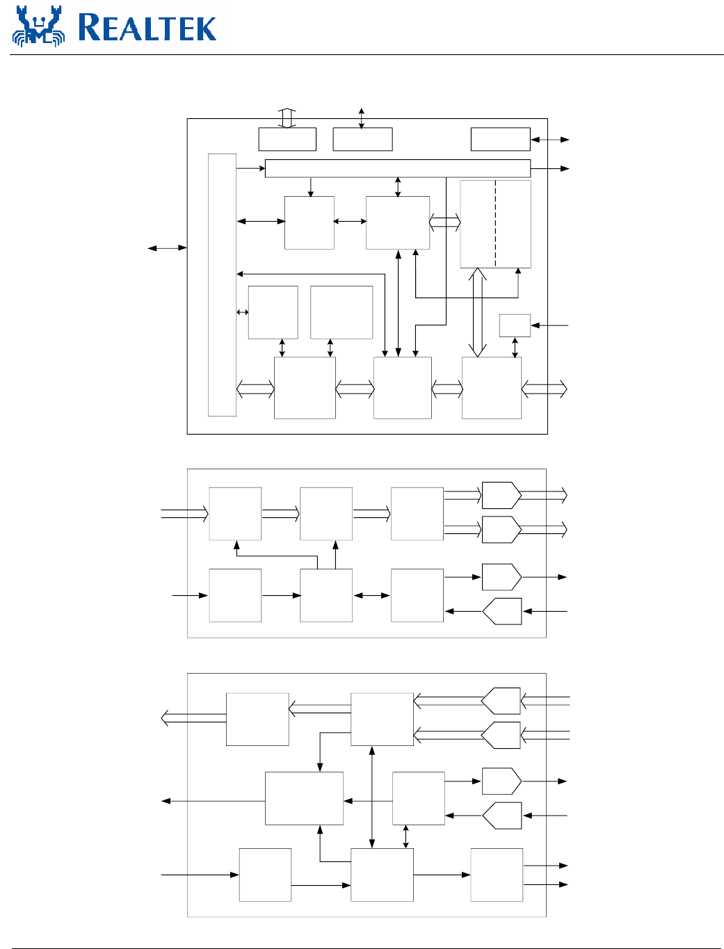
4. Block Diagrams
MAC/BBP
Interface
Interrupt
Control
Logic
FIFO
Transmit/
Receive
Logic
Interface
RTS, CTS,
ACK Frame
Generator
FIFO
Control
Logic
Frame Type
Discriminator
Power and TX/RX Timing Control Logic
Register
Frame Length
Register
EEPROM
Interface LED Driver
Scrambler
TXI
MAC
BBP, TX Section
CCA/
NAV From BBP
WEP/
TKIP/
AES
Engine
Checksum
Logic
Serial
Control Radio and
Synthesizer
Control
Coding Digital
Filter TXQ
TXDET
TXAGC
TX AGC
Control
Descrambler
RXI
MAC/BBP
Interface Decoding
ADC
RXQ
DAC
RSSI
RXAGC
RX AGC
Control
ADC
ADC
Clear Channel
Assessment/
Signal Quality
Antenna
Diversity
Control
TX State
Machine
Register
From
MAC
RX State
Machine
Register
From
MAC
To MAC
PCI
Express
Interface
BBP, RX Section
MAC/BBP
Interface DAC
ADC
DAC
DAC
ANTSELB
ANTSEL
Figure 1. Block Diagram
RTL8187SE
Datasheet
Single-Chip Wireless LAN Network Interface Controller
w/PCI Express Interface
6Track ID: JATR-1076-21 Rev. 1.0
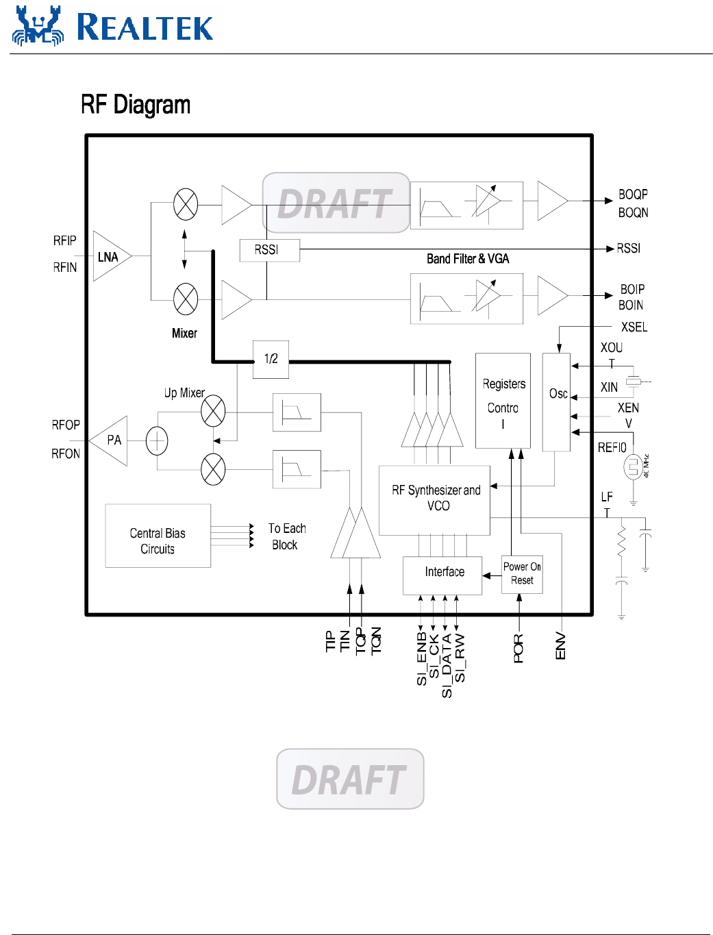
Figure 2. RF Block Diagram
RTL8187SE
Datasheet
Single-Chip Wireless LAN Network Interface Controller
w/PCI Express Interface
7Track ID: JATR-1076-21 Rev. 1.0
5. Pin Assignments
1 2 3 4 5 6 7 8 9 10 11 12 13 14 15 16
48 47 46 45 44 43 42 41 40 39 38 37 36 35 34 33
RFOP
RFON
RFIP
PAPE
VAA33
TRSWP
VCTRL_LDO
VDD
PERSTB
VAA33
HSIP
AGND
VDD
CLKREQB
TRIN
ANTENSWN
VDD
HSIN
WAKEB
GND
HSOP
DA8_DEBUG
TRQN
VAA33
VDD33
RFIN
TRSWN
VAA33
EXTRSTB
BTSTAT
VAA33
VAA33
VAA33
GND
EEDI/AUX
LED1
REFCLK+
HSON
REFCLK-
TRQP
TSSI
LLLLLLL TXXXV
RTL8187SE
TRIP
VAA33
R15K
AGND
XO
XI
VD_DIV
VD_CBC
49
50
51
52
53
54
55
56
57
58
59
60
61
62
63
64
32
31
30
29
28
27
26
25
24
23
22
21
20
19
18
17
VDD33
ANTENSWP
WLRXIND
ISOLATEB
AGND
BTPRI
GND
EEDO
EESK/9356SEL
EECS
WLACT
LED0
GND
65 GND (Exposed Pad)
GND
VDD
Figure 3. Pin Assignments
5.1. Package Identification
Green package is indicated by a ‘G’ in the location marked ‘T’ in Figure 3.

RTL8187SE
Datasheet
Single-Chip Wireless LAN Network Interface Controller
w/PCI Express Interface
8Track ID: JATR-1076-21 Rev. 1.0
6. Pin Descriptions
The following signal type codes are used in the tables:
I: Input AO: Analog Output
DI: Digital Input AIO: Analog Input/Output
AI: Analog Input T/S: Tri-State Bi-Directional Input/Output
O: Output S/T/S: Sustained Tri-State
DO: Digital Output O/D: Open Drain
6.1. Power Management/Isolation Interface
Table 1. Power Management/Isolation Interface
Symbol Type Pin No Description
WAKEB O/D 33 Power Management Event: Open drain, active low.
Used to reactivate the PCI Express slot’s main power rails and reference clocks.
ISOLATEB DI 18 Isolate Pin: Active low.
Used to isolate the RTL8187SE-GR from the PCI Express bus. The
RTL8187SE-GR will not drive its PCI Express outputs (excluding WAKEB) and
will not sample its PCI Express input as long as the Isolate pin is asserted.
6.2. PCI Express Interface
Table 2. PCI Express Interface
Symbol Type Pin No Description
REFCLK+ I 40
REFCLK- I 39 PCI Express Differential Reference Clock Source: 100MHz ±300ppm.
HSOP O 43
HSON O 42 PCI Express Transmit Differential Pair.
HSIP I 47
HSIN I 46 PCI Express Receive Differential Pair.
PERSTB I 36 PCI Express Reset Signal: Active low.
When the PERSTB is asserted at power-on state, the RTL8187SE-GR returns
to a pre-defined reset state and is ready for initialization and configuration
after the de-assertion of the PERSTB.
CLKREQB O/D 34 Reference Clock Request Signal. This signal is used by the RTL8187SE-GR to
request starting of the PCI Express reference clock.

RTL8187SE
Datasheet
Single-Chip Wireless LAN Network Interface Controller
w/PCI Express Interface
9Track ID: JATR-1076-21 Rev. 1.0
6.3. EEPROM Interface
Table 3. EEPROM Interface
Symbol Type Pin No Description
EESK/9356SEL DO/DI 26 EESK in 93C46 (93C56) programming or auto-load mode.
Input Pin as 9356 Select Pin at Initial Power-up.
When this pin is pulled high with a 10K resistor, the 93C56 EEPROM
is used to store the resource data for the RTL8187SE.
The RTL8187SE latches the status of this pin at power-up to
determine which EEPROM (93C46 or 93C56) is used.
After power on and GPIO_EN[5]=1, this pin is GPIO[5].
EEDI/AUX DO/DI 25 EEDI: Output to serial data input pin of EEPROM.
AUX: Input pin to detect if Aux. Power exists or not on initial
power-on. This pin should be connected to EEPROM. To support
wakeup from ACPI D3cold or APM power-down, this pin must be
pulled high to Aux. Power via a resistor. If this pin is not pulled high to
Aux. Power, the RTL8187SE assumes that no Aux. Power exists.
After power on and GPIO_EN[4]=1, this pin is GPIO[4].
EEDO DI 24 This pin is GPIO[3] after power on and GPIO_EN[3]=1, otherwise, it
is EEDO in 93C46 (93C56) programming or auto-load mode.
EECS DO 27 EEPROM Chip Select.
93C46 (93C56) chip select.
6.4. Power Pins
Table 4. Power Pins
Symbol Type Pin No Description
VDD33 P 21, 32 +3.3V (Digital).
VAA33 P 1, 2, 11, 48, 55, 58, 59,
62
+3.3V (Analog).
VDD P 12, 23, 37, 44 +1.8V.
GND P 13, 20, 22, 31, 38, 65 Ground (Digital).
AGND P 41, 45, 57 Ground (Analog).
VCTRL_LDO AO 10 Reserve this pin for external BJT option to generate 1.8V for digital
core circuit.
VD_CBC P 63 Reserved for external power transistor.
VD_DIV P 64 Reserved for external power transistor.

RTL8187SE
Datasheet
Single-Chip Wireless LAN Network Interface Controller
w/PCI Express Interface
10 Track ID: JATR-1076-21 Rev. 1.0
6.5. LED Interface
Table 5. LED Interface
Symbol Type Pin No Description
LED0 O 30 LED Pin.
a. PWRON: I2C_CK
b. After PWRON & LED_CONTROL=3’h7: GPIO[0]
c. Other: LED0
LED1 O 35 LED Pin.
a. PWRON: I2C_IO
b. After PWRON & LED_CONTROL=3’h7: GPIO[1]
c. Other: LED1
6.6. Baseband and RF Pins
Table 6. Baseband and RF Pins
Symbol Type Pin No Description
RFOP AO 3
RFON AO 4 2.4GHz Differential RF Power Amplifier Output.
RFIN AI 5
RFIP AI 6 2.4GHz Differential RF Input.
PAPE DO 7 Enable Control for Optional External Power Amplifier
TRSWN DO 8
TRSWP DO 9 Control Signals for Optional External RF T/R Switch
ANTENSWP DO 15
ANTENSWN DO 16 Control Signals for Antenna Switch
TSSI AI 50 Transmit Signal Strength Indication From External Power Amplifier
TRQP AIO 51 Via register setting, can be programmed to one of the following four types of pins:
RF TXQP: Input pin for RF TX test RF RXQP: Output pin for RF RX test
AFE TXQP: Output pin for DAC test AFE RXQP: Input pin for ADC test
TRQN AIO 52 Via register setting, can be programmed to one of the following four types of pins:
RF TXQN: Input pin for RF TX test RF RXQN: Output pin for RF RX test
AFE TXQN: Output pin for DAC test AFE RXQN: Input pin for ADC test
TRIN AIO 53 Via register setting, can be programmed to one of the following four types of pins:
RF TXIN: Input pin for RF TX test RF RXIN: Output pin for RF RX test
AFE TXIN: Output pin for DAC test AFE RXIN: Input pin for ADC test
TRIP AIO 54 Via register setting, can be programmed to one of the following four types of pins:
RF TXIP: Input pin for RF TX test RF RXIP: Output pin for RF RX test
AFE TXIP: Output pin for DAC test AFE RXIP: Input pin for ADC test

RTL8187SE
Datasheet
Single-Chip Wireless LAN Network Interface Controller
w/PCI Express Interface
11 Track ID: JATR-1076-21 Rev. 1.0
6.7. Bluetooth Co-Existence Pins
Table 7. Bluetooth Co-Existence Pins
Symbol Type Pin No Description
WLRXIND O 17 Wireless LAN RX Activity Indicator
BTPRI IO 19 Bluetooth Priority Pin
This pin is GPIO[2] after power on and GPIO_EN[2]=1, otherwise, this pin is
BTPRI. The BTPRI signal indicates when an important Bluetooth packet is being
transmitted or received.
BTSTAT IO 28 Bluetooth Status
This pin is GPIO[6] after power on and GPIO_EN[6]=1, otherwise, this pin is
BTSTAT. The BTSTAT signal indicates when normal Bluetooth packets are being
transmitted or received.
WLACT O 29 WLAN Activity
The WLAN_Active signal indicates when WLAN is either transmitting or
receiving in the 2.4GHz ISM band.
6.8. Clock and Other Pins
Table 8. Clock and Other Pins
Symbol Type Pin No Description
R15K IO 56 This pin must be pulled low by a 15K resistor.
XI I 60 Input of 40MHz Clock Reference.
XO O 61 Output of 40MHz Clock Reference.
EXTRSTB I 14 External Reset Pin: Active Low.
DA8_DEBUG O 49 Debug Pin.
7. EEPROM (93C46 or 93C56) Contents
The RTL8187SE supports the attachment of an external EEPROM. The 93C46 is a 1Kbit EEPROM
(the 93C56 is a 2Kbit EEPROM). The EEPROM interface provides the ability for the RTL8187SE to read
from, and write data to, an external serial EEPROM device. Values in the external EEPROM allow default
fields in PCI configuration space and IO space to be overridden following an internal power on reset, or
software EEPROM auto-load command. The RTL8187SE will auto-load values from the EEPROM to
these fields in configuration space and IO space. If the EEPROM is not present, the RTL8187SE
initialization uses default values for the appropriate Configuration and Operational Registers. Software can
read and write to the EEPROM using ‘bit-bang’ accesses via the 9346CR Register.
Note: It is suggested to obtain Realtek approval before changing the default settings of the EEPROM.

RTL8187SE
Datasheet
Single-Chip Wireless LAN Network Interface Controller
w/PCI Express Interface
12 Track ID: JATR-1076-21 Rev. 1.0
8. PCI EXPRESSTM
8.1. PCI EXPRESS Bus Interface
The RTL8187SE is compliant with PCI ExpressTM Base Specification Revision 1.1, and runs at 2.5GHz
signaling rate with X1 link width, i.e., one transmit and one receive differential pairs. The RTL8187SE
supports 4 types of PCI Express messages; interrupt messages, error messages, power management
messages, and hot-plug messages. PCI Express lane polarity reversal and link reversal are also supported to
ease PCB layout constraints.
8.1.1. PCI Express Transmitter
The RTL8187SE’s PCI ExpressTM block receives digital data recovered from the WLAN MAC interface
and performs data scrambling with Linear Feedback Shift Register (LFSR) and 8B/10B coding technology
into 10-bit code groups. Data scrambling is used to reduce the possibility of electrical resonance on the link,
and 8B/10B coding technology is used to benefit embedded clocking, error detection, and DC balance by
sacrificing the 25 percent overhead to the system through the addition of 2 extra bits. Then, the data code
groups are passed through its serializer for packet framing to generate 2.5 Gbps serial data and transmitted
onto PCB trace to its upstream device via differential driver.
8.1.2. PCI Express Receiver
The RTL8187SE’s PCI ExpressTM block receives 2.5Gbps serial data from its upstream device to generate
parallel data. The receiver’s PLL circuits are resynchronized to maintain bit and symbol lock. Through
8B/10B decoding technology and data descrambling, the original digital data is able to be recovered and
then the data is passed to the RTL8187SE’s internal WLAN MAC to be transmitted on the air.

RTL8187SE
Datasheet
Single-Chip Wireless LAN Network Interface Controller
w/PCI Express Interface
13 Track ID: JATR-1076-21 Rev. 1.0
8.2. PCI Configuration Space Table
Note: The following table assumes Power Management is enabled.
Table 9. PCI Configuration Space Table
No. Name Type Bit7 Bit6 Bit5 Bit4 Bit3 Bit2 Bit1 Bit0
00h VID R VID7 VID6 VID5 VID4 VID3 VID2 VID1 VID0
01h R VID15 VID14 VID13 VID12 VID11 VID10 VID9 VID8
02h DID R DID7 DID6 DID5 DID4 DID3 DID2 DID1 DID0
03h R DID15 DID14 DID13 DID12 DID11 DID10 DID9 DID8
04h Command R 0 PERRSP 0 0 0 BMEN MEMEN IOEN
W - PERRSP - - - BMEN MEMEN IOEN
05h R 0 0 0 0 0 IntDisable 0 SERREN
W - - - - - IntDisable - SERREN
06h Status R 0 0 0 1 IntSt 0 0 0
07h R DPERR SSERR RMABT RTABT STABT 0 0 DPD
W DPERR SSERR RMABT RTABT STABT - - DPD
08h Revision ID R 0 0 1 0 0 0 1 0
09h PIFR R 0 0 0 0 0 0 0 0
0Ah SCR R 1 0 0 0 0 0 0 0
0Bh BCR R 0 0 0 0 0 0 1 0
0Ch CLS RW CLS7 CLS6 CLS5 CLS4 CLS3 CLS2 CLS1 CLS0
0Dh LTR R 0 0 0 0 0 0 0 0
0Eh HTR R 0 0 0 0 0 0 0 0
0Fh BIST R 0 0 0 0 0 0 0 0
10h IOAR R 0 0 0 0 0 0 0 IOIN
W - - - - - - - -
11h RW IOAR15 IOAR14 IOAR13 IOAR12 IOAR11 IOAR10 IOAR9 IOAR8
12h RW IOAR23 IOAR22 IOAR21 IOAR20 IOAR19 IOAR18 IOAR17 IOAR16
13h RW IOAR31 IOAR30 IOAR29 IOAR28 IOAR27 IOAR26 IOAR25 IOAR24
14h-
17h
Reserved
18h-
1Fh
Reserved
20h-
27h
Reserved
28h-
2Bh
Reserved
2Ch SVID R SVID7 SVID6 SVID5 SVID4 SVID3 SVID2 SVID1 SVID0
2Dh R SVID15 SVID14 SVID13 SVID12 SVID11 SVID10 SVID9 SVID8
2Eh SMID R SMID7 SMID6 SMID5 SMID4 SMID3 SMID2 SMID1 SMID0
2Fh R SMID15 SMID14 SMID13 SMID12 SMID11 SMID10 SMID9 SMID8
30h BMAR R 0 0 0 0 0 0 0 BROMEN
W - - - - - - - BROMEN
31h R BMAR15 BMAR14 BMAR13 BMAR12 BMAR11 0 0 0
W BMAR15 BMAR14 BMAR13 BMAR12 BMAR11 - - -
32h RW BMAR23 BMAR22 BMAR21 BMAR20 BMAR19 BMAR18 BMAR17 BMAR16
33h RW BMAR31 BMAR30 BMAR29 BMAR28 BMAR27 BMAR26 BMAR25 BMAR24
34h Cap_Ptr R 0 1 0 0 0 0 0 0
35h-
3Bh
Reserved
3Ch ILR RW IRL7 ILR6 ILR5 ILR4 ILR3 ILR2 ILR1 ILR0
3Dh IPR R 0 0 0 0 0 0 0 1
3Eh MNGNT R 0 0 0 0 0 0 0 0

RTL8187SE
Datasheet
Single-Chip Wireless LAN Network Interface Controller
w/PCI Express Interface
14 Track ID: JATR-1076-21 Rev. 1.0
No. Name Type Bit7 Bit6 Bit5 Bit4 Bit3 Bit2 Bit1 Bit0
3Fh MXLAT R 0 0 0 0 0 0 0 0
40h PMID R 0 0 0 0 0 0 0 1
41h NextPtr R 0 1 0 1 0 0 0 0
42h R Aux_I_b1 Aux_I_b0 DSI Reserved PMECLK Version
43h
PMC
R PME_D3cold PME_D3hot PME_D2 PME_D1 PME_D0 D2 D1 Aux_I_b2
R 0 0 0 0 0 0 Power State 44h
W - - - - - - Power State
R PME_Status - - - - - - PME_En45h
PMCSR
W PME_Status - - - - - - PME_En
46-
4Fh
Reserved
50h MSIID R 0 0 0 0 0 1 0 1
51h NextPtr R 0 1 1 1 0 0 0 0
R 64-bit
Address
Capable
Multiple Message Enable 0 0 0 MSI Enable
52h
W - Multiple Message Enable - - 0 MSI Enable
53h
Message
Control
Reserved. Always return 0
54h-
57h
Message
Address Low
RW 64-bit Interrupt Message Address Low
58h-
5Bh
Message
Address High
RW 64-bit Interrupt Message Address High
5Ch-
5Dh
Message Data RW 16-bit Message Data
5E-
6Fh
RESERVED
70h PCIEID R 0 0 0 1 0 0 0 0
71h NextPtr R 0 0 0 0 0 0 0 0
R 0 0 0 Legacy 0 0 0 1 72h-
73h
PCIE Cap.
R 0 0 0 0 0 0 0 0
R L0s_acpt_
latency[1]
L0s_acpt_
latency[0]
Entend_
tag_support
0 0 Max_payload_size_support
R Role Base
Error rpt
0 0 0 L1_acpt_
latency[2]
L1_acpt_
latency[1]
L1_acpt_
latency[0]
L0s_acpt_la
tency[2]
R 0 0 0 0 0 0 0 0
74h-
77h
Device
Capability
Register
R 0 0 0 0 0 0 0 0
RW Max_payload_size Relaxed_
ordering_en
Unsupport_
rqst_rpt_en
Fatal_err_
rpt_en
Non_fatal_
err_rpt_en
Correct-
able_err_
rpt_en
78h-
79h
Device
Control
Register
RW 0 Max_read_request_size No_snoop_en Auxpwr_
PM_en
0 Entend_
tag_en
R 0 0 Transact_
ion_pending
AuxPwr_det Upsupport_
rqst_det
Fatal_err_det Non_fatal_
err_det
Correct-
able_err_det
7Ah
W 0 0 - - Upsupport_
rqst_det
Fatal_err_det Non_fatal_err
_det
Correcta-
ble_err_det
7Bh
Device Status
Register
R 0 0 0 0 0 0 0 0
7Ch R 0 0 0 1 0 0 0 1
7Dh R L1_exit_
lat[0]
L0s_exit_
lat[2]
L0s_exit_
lat[1]
L0s_exit_
lat[0]
ASPM_support 0 0
7Eh R 0 0 0 0 0 Clock_PM L1_exit_
lat[2]
L1_exit_
lat[1]0
7Fh
Link
Capability
Register
R 0 0 0 0 0 0 0 0

RTL8187SE
Datasheet
Single-Chip Wireless LAN Network Interface Controller
w/PCI Express Interface
15 Track ID: JATR-1076-21 Rev. 1.0
No. Name Type Bit7 Bit6 Bit5 Bit4 Bit3 Bit2 Bit1 Bit0
R Extended_
sync
Common_
clock
0 0 RCB 0 ASPM_control 80h
W Extended_
sync
Common_
clock
0 0 RCB 0 ASPM_control
R 0 0 0 0 0 0 0 Enable
clock_PM
81h
Link Control
Register
W 0 0 0 0 0 0 0 Enable
clock_PM
82h R 0 0 0 1 0 0 0 1
83h
Link Status
Register R 0 0 0 Slot_clock_
cfg
0 0 0 0
84h R Slot power
Limit[0]
Hot-Plug
Capable
Hot-Plug
Surprise
Power
indicator
present
Attn indicator
present
MRL sensor
present
Power control
present
Attn button
present
85h R Slot power
Limit scale[0]
Slot power
Limit[7]
Slot power
Limit[6]
Slot power
Limit[5]
Slot power
Limit[4]
Slot power
Limit[3]
Slot power
Limit[2]
Slot power
Limit[1]
86h R Physical slot
Number[4]
Physical
slot Number[3]
Physical slot
Number[2]
Physical slot
Number[1]
Physical slot
Number[0]
No common
Complete
support
Electromecha
nical interlock
present
Slot power
Limit
scale[1]
87h
Slot
Capability
Register
R Physical slot
Number[12]
Physical slot
Number[11]
Physical slot
Number[1]
Physical slot
Number[9]
Physical slot
Number[8]
Physical slot
Number[7]
Physical slot
Number[6]
Physical slot
Number[5]
88h RW Attn Indicator
Control[1]
Attn Indicator
Control[0]
Hot-Plug
Interrupt
Enable
Command
Completed
interrupt
Enable
Presence
Detect
Changed
Enable
MRL Sensor
Changed
Enable
Power Fault
Detected
Enable
Attn Bottom
Pressed
Enable
89h
Slot Control
Register
RW - - - Data Link
Layer State
Changed
Enable
Electromecha
nical Interlock
Control
Power
Controller
Control
Power
Indicator
Control[1]
Power
Indicator
Control[0]
8Ah R Electromecha
nical Interlock
Status
Presence Detect
State
MRL Sensor
State
Command
Completed
Presence
Detect
Changed
MRL Sensor
Changed
Power Fault
Detected
Attn Botton
pressed
8Bh
Slot Status
Register
R Reversed Data Link
Layer State
Changed
8Ch-
FFh
Reversed

RTL8187SE
Datasheet
Single-Chip Wireless LAN Network Interface Controller
w/PCI Express Interface
16 Track ID: JATR-1076-21 Rev. 1.0
8.3. PCI Configuration Space Functions
The PCI configuration space is intended for configuration, initialization, and catastrophic error handling
functions. The functions of the configuration space of the RTL8187SE are described below.
VID: Vendor ID. This field will be set to a value corresponding to a PCI Vendor ID in the external
EEPROM. If there is no EEPROM, this field will default to a value of 10ECh, which is Realtek
Semiconductor’s PCI Vendor ID.
DID: Device ID. This field will be set to a value corresponding to a PCI Device ID in the external
EEPROM. If there is no EEPROM, this field will default to a value of 8185h.
Command: The command register is a 16-bit register used to provide coarse control over a device's ability
to generate and respond to PCI cycles.
Table 10. Command Register in PCI Configuration Space
Bit Symbol Description
15:11 - Reserved.
10 INTDIS Interrupt Disable.
This Bit enables/disables the RTL8187SE to assert Int# signal.
1: Force disable assertion of the Int# signal.
0: Enable enable assertion of the Int# signal (default value after PCI reset)
9 FBTBEN Fast Back-To-Back Enable. Does not apply to PCI Express. Must be hardwired to 0.
8 SERREN System Error Enable.
When set to 1, enables reporting of Non-fatal and Fatal errors detected by the device to the Root
Complex. Note that errors are reported if enabled either through this bit or through the
PCI-Express specific bits in the Device Control register.
7 ADSTEP Address/Data Stepping. Does not apply to PCI Express. Must be hardwired to 0.
6 PERRSP Parity Error Response.
In the Status register, the Master Data Parity Error bit is set by a Requester if its Parity Error
Response bit is set and either of the following two conditions occurs:
- If the Requester receives a poisoned Completion.
- If the Requester poisons a write request.
If the Parity Error Response bit is cleared, the Master Data Parity Error status bit is never set.
5 VGASNOOP VGA Palette SNOOP. Does not apply to PCI Express. Must be hardwired to 0.
4 MWIEN Memory Write and Invalidate Cycle Enable.
Does not apply to PCI Express. Must be hardwired to 0.
3 SCYCEN Special Cycle Enable. Does not apply to PCI Express. Must be hardwired to 0.
2 BMEN Bus Master Enable.
When set to 1, the RTL8187SE is capable of acting as a PCI bus master. When set to 0, it is
prohibited from acting as a bus master.
For normal operations, this bit must be set by the system BIOS.
1 MEMEN Memory Space Access. When set to 1, the RTL8187SE responds to memory space accesses.
When set to 0, the RTL8187SE ignores memory space accesses.
0 IOEN IO Space Access. When set to 1, the RTL8187SE responds to IO space accesses. When set to 0,
the RTL8187SE ignores IO space accesses.

RTL8187SE
Datasheet
Single-Chip Wireless LAN Network Interface Controller
w/PCI Express Interface
17 Track ID: JATR-1076-21 Rev. 1.0
8.4. PCI Configuration Space Status
8.4.1. Status
The status register is a 16-bit register used to record status information for PCI bus related events. Reads to
this register behave normally. Writes are slightly different in that bits can be reset, but not set.
Table 11. PCI Configuration Space Status
Bit Symbol Description
15 DPERR Detected Parity Error.
This bit is set by the RTL8187SE whenever it receives a Poisoned Transaction Layer Packet
(TLP), regardless of the state the Parity Error Enable bit. Default value of this field is 0.
14 SSERR Signaled System Error.
This bit is set when the RTL8187SE sends an ERR_FATAL or ERR_NONFATAL Message, and
the SERR Enable bit in the Command register is 1. Default value of this field is 0.
13 RMABT Received Master Abort.
This bit is set when the RTL8187SE receives a Completion with Unsupported Request
Completion Status. Default value of this field is 0.
12 RTABT Received Target Abort.
This bit is set when the RTL8187SE receives a Completion with Completer Abort Completion
Status. Default value of this field is 0.
11 STABT Signaled Target Abort.
This bit is set when the RTL8187SE completes a Request using Completer Abort Completion
Status. Default value of this field is 0.
10:9 DST1~0 Device Select Timing. Does not apply to PCI Express. Must be hardwired to 0.
8 DPD Data Parity Error Detected.
This bit is set by the RTL8187SE if its Parity Error Enable bit is set and either of the following
two conditions occurs:
- Requestor receives a Completion marked poisoned
- Requestor poisons a write Request
If the Parity Error Enable bit is cleared, this bit is never set. Default value of this field is 0.
7 FBBC Fast Back-To-Back Capable. Does not apply to PCI Express. Must be hardwired to 0.
6 - Reserved.
5 66MHz 66MHz Capable. Does not apply to PCI Express. Must be hardwired to 0.
4 NewCap Capability List.
Indicates the presence of an extended capability list item. Since all PCI Express devices are
required to implement the PCI Express capability structure, this bit must be set to 1.
3 INTSTS Interrupt Status.
This bit reflects the interrupt status of the RTL8187SE.
Unlike ISR bits, this bit is a read-only bit and cannot be reset by writing a 1 to this bit. The only
way to reset this bit is to reset the ISR register.
The setting of the ‘Interrupt Disable’ bit in the Command Register has no effect on the state of
the ‘Interrupt Status’ bit.
Only when the ‘Interrupt Disable’ bit is a 0 and the ‘Interrupt Status’ bit is a 1, will the
RTL8187SE’s Int# signal be asserted.
2:0 - Reserved.

RTL8187SE
Datasheet
Single-Chip Wireless LAN Network Interface Controller
w/PCI Express Interface
18 Track ID: JATR-1076-21 Rev. 1.0
8.4.2. RIDR (Revision ID Register)
The Revision ID register is an 8-bit register that specifies the RTL8187SE controller revision number.
8.4.3. PIFR (Programming Interface Register)
The programming interface register is an 8-bit register that identifies the programming interface of the
RTL8187SE controller. The PCI 2.1 specification does not define a specific value for network devices. In
the RTL8187SE controller this is PIFR = 00h.
8.4.4. SCR (Sub-Class Register)
The Sub-Class Register is an 8-bit register that identifies the function of the RTL8187SE. SCR=0x80
indicates that the RTL8187SE is identified as ‘other network controller’.
8.4.5. BCR (Base-Class Register)
The Base-Class Register is an 8-bit register that broadly classifies the function of the RTL8187SE.
BCR=02h indicates that the RTL8187SE is a network controller.
8.4.6. CLS (Cache Line Size)
This field is implemented by PCI Express devices as a read-write field for legacy compatibility purposes
but has no impact on any PCI Express device functionality.
8.4.7. LTR (Latency Timer Register)
This register is also referred to as primary latency timer for Type 1 Configuration Space header devices.
The primary/master latency timer does not apply to PCI Express. This register must be hardwired to 0.
8.4.8. HTR (Header Type Register)
Reads will return a 0, writes are ignored.
8.4.9. BIST (Built-In Self-Test)
Reads will return a 0, writes are ignored.

RTL8187SE
Datasheet
Single-Chip Wireless LAN Network Interface Controller
w/PCI Express Interface
19 Track ID: JATR-1076-21 Rev. 1.0
8.4.10. IOAR (Input Output Address Register)
This register specifies the BASE IO address, which is required to build an address map during
configuration. It also specifies the number of bytes required as well as an indication that it can be mapped
into IO space.
Table 12. Input Output Address Register
Bit Symbol Description
31:8 IOAR31~8 Base Input Output Address.
This is set by software to the Base IO address for the operational register map.
7:2 IOSIZE Input Output Size Indication.
Read back as 0. This allows the PCI bridge to determine that the RTL8187SE requires 256 bytes
of IO space.
1 - Reserved.
0 IOIN IO Space Indicator.
Read only. Set to 1 by the RTL8187SE to indicate that it is capable of being mapped into IO
space.
8.4.11. MEMAR (Memory Address Register)
This register specifies the base memory address for memory accesses to the RTL8187SE operational
registers. This register must be initialized prior to accessing any RTL8187SE register with memory access.
Table 13. Memory Address Register
Bit Symbol Description
31:8 MEM31~8 Base Memory Address.
This is set by software to the base address for the operational register map.
7:4 MEMSIZE Memory Size.
These bits return 0, which indicates that the RTL8187SE requires 256 bytes of Memory Space.
3 MEMPF Memory Pre-Fetchable.
Read only. Set to 0 by the RTL8187SE.
2:1 MEMLOC Memory Location Select.
Read only. Set to 0 by the RTL8187SE. This indicates that the base register is 32 bits wide and
can be placed anywhere in the 32-bit memory space.
0 MEMIN Memory Space Indicator.
Read only. Set to 0 by the RTL8187SE to indicate that it is capable of being mapped into memory
space.
8.4.12. CISPtr (CardBus Card Information Structure Pointer)
CardBus CIS Pointer. This register does not apply to PCI Express. It must be read-only and must be
hardwired to 0.

RTL8187SE
Datasheet
Single-Chip Wireless LAN Network Interface Controller
w/PCI Express Interface
20 Track ID: JATR-1076-21 Rev. 1.0
8.4.13. SVID (Subsystem Vendor ID)
This field will be set to a value corresponding to the PCI Subsystem Vendor ID in the external EEPROM. If
there is no EEPROM, this field will default to a value of 10ECh (Realtek Semiconductor’s PCI Subsystem
Vendor ID).
8.4.14. SMID (Subsystem ID)
This field will be set to a value corresponding to the PCI Subsystem ID in the external EEPROM. If there is
no EEPROM, this field will default to a value of 8198h.
8.4.15. ILR (Interrupt Line Register)
The Interrupt Line Register is an 8-bit register used to indicate the routing of the interrupt. It is written by
the POST software to set an interrupt line for the RTL8187SE.
8.4.16. IPR (Interrupt Pin Register)
The Interrupt Pin register is an 8-bit register indicating the interrupt pin used by the RTL8187SE. The
RTL8187SE uses INTA interrupt pin. Read only. IPR = 01h.
8.4.17. MNGNT (Minimum Grant Timer: Read only)
This register does not apply to PCI Express. It must be read-only and must be hardwired to 0.
8.4.18. MXLAT (Maximum Latency Timer: Read only)
This register does not apply to PCI Express. It must be read-only and must be hardwired to 0.
8.5. Default Value After Power-On (RSTB Asserted)
Table 14. PCI Configuration Space Table
No. Name Type Bit7 Bit6 Bit5 Bit4 Bit3 Bit2 Bit1 Bit0
00h VID R 1 1 1 0 1 1 0 0
01h R 0 0 0 1 0 0 0 0
02h DID R 1 0 0 0 0 1 0 1
03h R 1 0 0 0 0 0 0 1
04h Command R 0 0 0 0 0 0 0 0
W - PERRSP - MWIEN - BMEN MEMEN IOEN
05h R 0 0 0 0 0 0 0 0
W - - - - - - - SERREN
06h Status R 0 0 0 NewCap 0 0 0 0
07h R 0 0 0 0 0 0 1 0
W DPERR SSERR RMABT RTABT STABT - - DPD
08h Revision
ID R 0 0 1 0 0 0 1 0
09h PIFR R 0 0 0 0 0 0 0 0
0Ah SCR R 1 0 0 0 0 0 0 0

RTL8187SE
Datasheet
Single-Chip Wireless LAN Network Interface Controller
w/PCI Express Interface
21 Track ID: JATR-1076-21 Rev. 1.0
No. Name Type Bit7 Bit6 Bit5 Bit4 Bit3 Bit2 Bit1 Bit0
0Bh BCR R 0 0 0 0 0 0 1 0
0Ch CLS RW 0 0 0 0 0 0 0 0
0Dh LTR R 0 0 0 0 0 0 0 0
W LTR7 LTR6 LTR5 LTR4 LTR3 LTP2 LTR1 LTR0
0Eh HTR R 0 0 0 0 0 0 0 0
0Fh BIST R 0 0 0 0 0 0 0 0
10h IOAR R 0 0 0 0 0 0 0 1
11h RW 0 0 0 0 0 0 0 0
12h RW 0 0 0 0 0 0 0 0
13h RW 0 0 0 0 0 0 0 0
14h MEMAR R 0 0 0 0 0 0 0 0
15h RW 0 0 0 0 0 0 0 0
16h RW 0 0 0 0 0 0 0 0
17h RW 0 0 0 0 0 0 0 0
18h~
27h -RESERVED (ALL 0)
28h R 0 0 0 0 0 0 0 0
29h R 0 0 0 0 0 0 0 0
2Ah R 0 0 0 0 0 0 0 0
2Bh
CISPtr
R 0 0 0 0 0 0 0 0
2Ch SVID R 1 1 1 0 1 1 0 0
2Dh R 0 0 0 1 0 0 0 0
2Eh SMID R 1 0 0 0 0 1 0 1
2Fh R 1 0 0 0 0 0 0 1
30h BMAR R 0 0 0 0 0 0 0 0
W - - - - - - - BROMEN
31h R 0 0 0 0 0 0 0 0
W BMAR15 BMAR14 BMAR13 BMAR12 BMAR11 - - -
32h RW 0 0 0 0 0 0 0 0
33h RW 0 0 0 0 0 0 0 0
34h Cap-Ptr R Ptr7 Ptr6 Ptr5 Ptr4 Ptr3 Ptr2 Ptr1 Ptr0
35h~
3Bh -RESERVED (ALL 0)
3Ch ILR RW 0 0 0 0 0 0 0 0
3Dh IPR R 0 0 0 0 0 0 0 1
3Eh MNGNT R 0 0 0 0 0 0 0 0
3Fh MXLAT R 0 0 0 0 0 0 0 0
40h~
FFh -RESERVED (ALL 0)

RTL8187SE
Datasheet
Single-Chip Wireless LAN Network Interface Controller
w/PCI Express Interface
22 Track ID: JATR-1076-21 Rev. 1.0
8.6. PCI Power Management Functions
The RTL8187SE is compliant with ACPI (Rev 2.0), PCI Power Management (Rev. 1.2), and Network
Device Class Power Management Reference Specification (V1.0a), such as to support an Operating
System-Directed Power Management (OSPM) environment.
The RTL8187SE can monitor the network for a Wakeup Frame, a Magic Packet, or a Re-LinkOk, and
notify the system via PME# when such a packet or event occurs. Then the system can be restored to a
normal state to process incoming jobs.
When the RTL8187SE is in power down mode (D1 ~ D3):
The Rx state machine is stopped, and the RTL8187SE monitors the network for wakeup events such as
a Magic Packet, Wakeup Frame, and/or Re-LinkOk, in order to wake up the system. When in power
down mode, the RTL8187SE will not reflect the status of any incoming packets in the ISR register and
will not receive any packets into the Rx FIFO buffer.
The FIFO status and packets that have already been received into the Rx FIFO before entering power
down mode are held by the RTL8187SE.
Transmission is stopped. PCI bus master mode is stopped. The Tx FIFO buffer is held.
After restoration to a D0 state, the RTL8187SE transfers data that was not moved into the Tx FIFO
buffer during power down mode. Packets that were not transmitted completely last time are
re-transmitted.
The D3cold_support_PME bit (bit15, PMC register) and the Aux_I_b2:0 bits (bit8:6, PMC register) in PCI
configuration space depend on the existence of Aux power (bit15, PMC) = 1.
If EEPROM D3cold_support_PME bit (bit15, PMC) = 0, the above 4 bits are all 0’s.
Example:
If EEPROM D3c_support_PME = 1:
If aux. power exists, then PMC in PCI config space is the same as EEPROM PMC
(if EEPROM PMC = C3 F7, then PCI PMC = C3 F7)
If aux. power is absent, then PMC in PCI config space is the same as EEPROM PMC except the above
4 bits are all 0’s (if EEPROM PMC = C3 F7, then PCI PMC = 03 76)
In the above case, if wakeup support is desired when main power is off, it is suggested that the EEPROM
PMC be set to C3 F7 (Realtek EEPROM default value).

RTL8187SE
Datasheet
Single-Chip Wireless LAN Network Interface Controller
w/PCI Express Interface
23 Track ID: JATR-1076-21 Rev. 1.0
If EEPROM D3c_support_PME = 0:
If aux. power exists, then PMC in PCI config space is the same as EEPROM PMC
(if EEPROM PMC = C3 77, then PCI PMC = C3 77)
If aux. power is absent, then PMC in PCI config space is the same as EEPROM PMC except the above
4 bits are all 0’s (if EEPROM PMC = C3 77, then PCI PMC = 03 76)
In the above case, if wakeup support is not desired when main power is off, it is suggested that the
EEPROM PMC be set to 03 76.
Magic Packet Wakeup occurs only when the following conditions are met:
The destination address of the received Magic Packet is acceptable to the RTL8187SE, e.g. a broadcast,
multicast, or unicast packet addressed to the current RTL8187SE adapter.
The received Magic Packet does not contain a CRC error.
The Magic bit (CONFIG3#5) is set to 1, the PMEn bit (CONFIG1#0) is set to 1, and the PME# can be
asserted in the current power state.
The Magic Packet pattern matches, i.e. 6 * FFh + MISC (can be none) + 16 * DID (Destination ID) in
any part of a valid WLAN packet.
A Wakeup Frame event occurs only when the following conditions are met:
The destination address of the received Wakeup Frame is acceptable to the RTL8187SE, e.g. a
broadcast, multicast, or unicast address to the current RTL8187SE adapter.
The received Wakeup Frame does not contain a CRC error.
The PMEn bit (CONFIG1#0) is set to 1.
The 16-bit CRC* of the received Wakeup Frame matches the 16-bit CRC* of the sample Wakeup Frame
pattern given by the local machine’s OS. Or, the RTL8187SE is configured to allow direct packet
wakeup, e.g. a broadcast, multicast, or unicast network packet.
*16-bit CRC: The RTL8187SE supports two normal wakeup frames (covering 64 mask bytes from offset 0 to
63 of any incoming network packet) and three long wakeup frames (covering 128 mask bytes from offset 0
to 127 of any incoming network packet).

RTL8187SE
Datasheet
Single-Chip Wireless LAN Network Interface Controller
w/PCI Express Interface
24 Track ID: JATR-1076-21 Rev. 1.0
The PME# signal is asserted only when the following conditions are met:
The PMEn bit (bit0, CONFIG1) is set to 1.
The PME_En bit (bit8, PMCSR) in PCI Configuration Space is set to 1.
The RTL8187SE may assert PME# in the current power state or in isolation state, depending on the
PME_Support (bit15-11) setting of the PMC register in PCI Configuration Space.
A Magic Packet, LinkUp, or Wakeup Frame has been received.
Note: Writing a 1 to the PME_Status (bit15) of the PMCSR register in the PCI Configuration Space clears
this bit and causes the RTL8187SE to stop asserting a PME# (if enabled).
When the device is in power down mode, e.g. D1~D3, the IO, and MEM spaces are all disabled. After a
RST# assertion, the device’s power state is restored to D0 automatically if the original power state was
D3cold. There is no hardware delay at the device’s power state transition. When in ACPI mode, the device
does not support PME (Power Management Enable) from D0 (this is the Realtek default setting of the PMC
register auto-loaded from EEPROM). The setting may be changed from the EEPROM, if required. The
RTL8187SE also supports the legacy LAN WAKE-UP function. The LWAKE pin is used to notify legacy
motherboards to execute the wake-up process whenever the device receives a wakeup event, such as Magic
Packet.
RTL8187SE
Datasheet
Single-Chip Wireless LAN Network Interface Controller
w/PCI Express Interface
25 Track ID: JATR-1076-21 Rev. 1.0
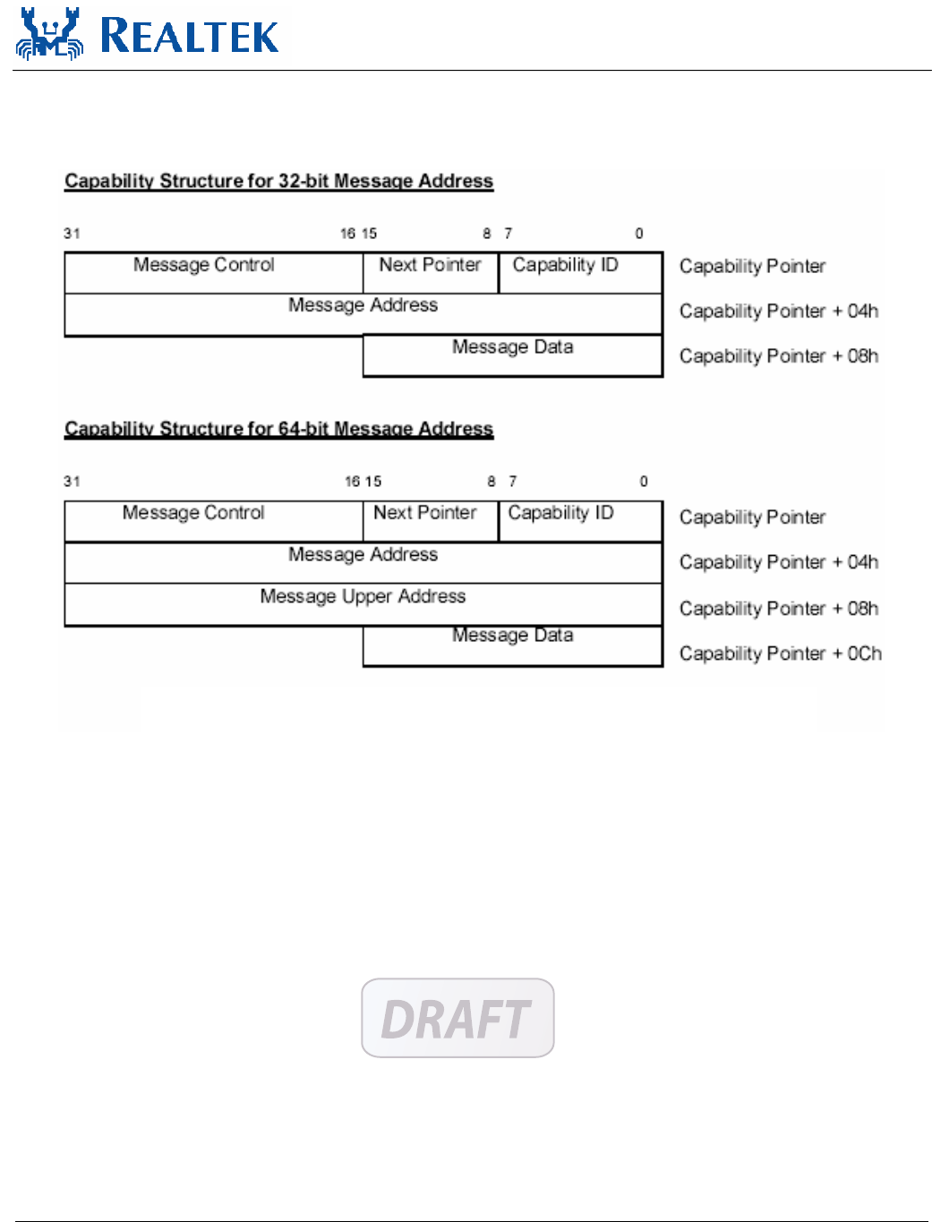
8.7. Message Signaled Interrupt (MSI)
8.7.1. MSI Capability Structure in PCI Configuration Space
Figure 4. Message Capability Structure

RTL8187SE
Datasheet
Single-Chip Wireless LAN Network Interface Controller
w/PCI Express Interface
26 Track ID: JATR-1076-21 Rev. 1.0
8.7.2. Message Control
Table 15. Message Control
Bits RW Field Description
15:8 RO Reserved Reserved. Always return 0
7 RO 64-Bit Address Capable 1: The RTL8187SE is capable of generating a 64-bit
message address.
0: The RTL8187SE is NOT capable of generating a 64-bit
message address.
This bit is read only and the RTL8187SE is set to 1.
System software (e.g., BIOS, OS) indicates to the RTL8187SE the
number of allocated messages/vectors (equal to or less than the
number of requested messages/vectors).
This field after PCI reset is ‘000’.
Encoding Number of Messages/Vectors
000 1
001 2
010 4
011 8
100 16
101 32
110 Reserved
6:4 RW Multiple Message Enable
111 Reserved
Indication to system software (e.g., BIOS, OS) of the number of
RTL8187SE requested vectors.
The RTL8187SE supports only one vector messages/vectors.
Encoding Number of Messages/Vectors
000 1
3:1 RO Multiple Message Capable
Others Reserved
0 RW MSI Enable 1: Enable MSI (Also the INTx pin is disabled automatically, MSI
and INTx are mutually exclusive), this bit is set by system software.
0: Disable MSI (Default value after power-on or PCI reset)
8.7.3. Message Address
Table 16. Message Address
Bits RW Field Description
31:02 RW Message Address System-Specified Message/Vector Address.
Low DWORD aligned address for MSI memory write transaction.
01:00 RO Reserved Always Return ‘00’.
This bit is read only.

RTL8187SE
Datasheet
Single-Chip Wireless LAN Network Interface Controller
w/PCI Express Interface
27 Track ID: JATR-1076-21 Rev. 1.0
8.7.4. Message Upper Address
Table 17. Message Upper Address
Bits RW Field Description
31:00 RW Message Upper Address System-Specified Message/Vector Upper Address.
Upper 32 bits of a 64-bit message/vector address.
This register is effective only when the DAC function is enabled,
i.e., 64-bit addressing is enabled; bit7 in Message Control register
is set.
If the contents of this register are 0, the RTL8187SE only performs
32-bit addressing for the memory write of the messages/vectors.
This bit is read/write.
8.7.5. Message Data
Table 18. Message Data
Bits RW Field Description
15:00 RW Message Data If the Message Enable bit is set, the message/vector data is driven
onto the lower word of the memory write transaction’s data phase.
This bit is read/write.

RTL8187SE
Datasheet
Single-Chip Wireless LAN Network Interface Controller
w/PCI Express Interface
28 Track ID: JATR-1076-21 Rev. 1.0
9. Functional Description
9.1. Transmit & Receive Operations
The RTL8187SE supports a descriptor-based buffer management that will significantly lower host CPU
utilization. The RTL8187SE supports an infinite number of consecutive transmit descriptors, and 64
consecutive receive descriptors, in memory.
There may be a maximum of five descriptor rings. Transmit descriptor rings consist of one beacon transmit
descriptor ring, one high priority descriptor ring, one normal priority descriptor ring, and one low priority
descriptor ring. Each transmit descriptor ring may consist of an infinite number of 8-double-word
consecutive descriptors, and the receive descriptor array may consist of up to sixty-four 4-double-word
consecutive descriptors. The start address of each descriptor group should be in 256byte alignment.
Software must pre-allocate enough buffers and configure all descriptor rings before transmitting and/or
receiving packets.
9.1.1. Transmit
The following describes what the Tx descriptor may look like, depending on different states in each Tx
descriptor.
Tx Descriptor Format (before transmitting, OWN=1, Tx command mode 1)
Table 19. Tx Descriptor Format (before transmitting, OWN=1, Tx command mode 1)
31 30 29 28 27 26 25 24 23 22 21 20 19 18 17 16 15 14 13 12 11 10 9 8 7 6 5 4 3 2 1 0
O
W
N
=
1
D
M
A
O
K
F
S
L
S
TXRATE
(4 bits)
R
T
S
E
N
RTSRAT
E
(4 bits)
C
T
S
E
N
M
O
R
E
F
R
A
G
S
P
L
C
P
N
O
_
E
N
C
R
Y
P
T
BSSID
_NO
TPKTSIZE (12 bits) Offset 0
L
E
N
G
E
X
T
Length (15 bits) RTSDUR (16 bits) Offset 4
TX_BUFFER_ADDRESS Offset 8
RTL8187SE
Datasheet
Single-Chip Wireless LAN Network Interface Controller
w/PCI Express Interface
29 Track ID: JATR-1076-21 Rev. 1.0
31 30 29 28 27 26 25 24 23 22 21 20 19 18 17 16 15 14 13 12 11 10 9 8 7 6 5 4 3 2 1 0
DURATION (16 bits) M
I
C
_
C
A
L
RSVD
(3 bits)
Frame_Length (12 bits) Offset 12
NEXT_TX_DESCRIPTOR_ADDRESS Offset 16
RATE_FALL
BACK_LIMIT
(5 bits)
RTS_RATE
_FALL
BACK_LI
MIT (4
bits)
RSVD
(4bits)
P
I
F
S
N
O
_
A
C
M
R
T
_
D
B
RETRY_LIMIT (8 bits) RTSAGC (8 bits) Offset 20
R
S
V
D
SPC A
N
T
E
N
N
A
AGC (8 bits) RSVD
(4bits)
DELAY_BOUND (16 bits) Offset 24
FRAG_QSIZE (16 bits) E
N
_
P
M
P
D
E
N
_
B
C
K
E
Y
BCKEY (6 bits) P
T
_
E
N
T
P
C
_
E
N
TPC
_PO
LA
RIT
Y
T
P
C
_
D
E
S
E
N
R
S
V
D
HW
Len
gth
Sele
ct
Offset 28

RTL8187SE
Datasheet
Single-Chip Wireless LAN Network Interface Controller
w/PCI Express Interface
30 Track ID: JATR-1076-21 Rev. 1.0
Table 20. Tx Status Descriptor
Offset# Bit# Symbol Description
0 31 OWN Ownership.
When set, this bit indicates that the descriptor is owned by the NIC, and the
data relative to this descriptor is ready to be transmitted. When cleared, it
indicates that the descriptor is owned by the host system. The NIC clears this
bit when the relative buffer data is transmitted. In this case, OWN=1.
0 30 DMA OK DMA OK.
Set by the driver, reset by the RTL8187SE when TX DMA OK. If IMR’s
corresponding bit is set and the driver sets this bit, the RTL8187SE resets this
bit and issues an interrupt right after DMA OK of the last segment (LS). If not,
the RTL8187SE just resets this bit without asserting an interrupt.
0 29 FS First Segment Descriptor.
When set, this bit indicates that this is the first descriptor of a Tx packet, and
that this descriptor is pointing to the first segment of the packet.
0 28 LS Last Segment Descriptor.
When set, indicates that this is the last descriptor of a Tx packet, and this
descriptor is pointing to the last segment of the packet.
0 27:24 TXRATE Tx Rate.
These five bits indicate the current frame’s transmission rate.
Bit 27 Bit 26 Bit 25 Bit 24
1Mbps 0 0 0 0
2Mbps 0 0 0 1
5.5Mbps 0 0 1 0
11Mbps 0 0 1 1
6Mbps 0 1 0 0
9Mbps 0 1 0 1
12Mbps 0 1 1 0
18Mbps 0 1 1 1
24Mbps 1 0 0 0
36Mbps 1 0 0 1
48Mbps 1 0 1 0
54Mbps 1 0 1 1
Reserved All other combinations
0 23 RTSEN RTS Enable.
Set to 1, indicates that an RTS/CTS handshake shall be performed at the
beginning of any frame exchange sequence where:
The frame is of type Data or Management,
the frame has a unicast address in the Address1 field,
and the length of the frame is greater than RTSThreshold.

RTL8187SE
Datasheet
Single-Chip Wireless LAN Network Interface Controller
w/PCI Express Interface
31 Track ID: JATR-1076-21 Rev. 1.0
Offset# Bit# Symbol Description
0 22:19 RTSRATE RTS Rate.
These four bits indicate the RTS frame’s transmission rate before transmitting
the current frame, and will be ignored if the RTSEN bit is set to 0.
Bit 22 Bit 21 Bit 20 Bit 19
1Mbps 0 0 0 0
2Mbps 0 0 0 1
5.5Mbps 0 0 1 0
11Mbps 0 0 1 1
6Mbps 0 1 0 0
9Mbps 0 1 0 1
12Mbps 0 1 1 0
18Mbps 0 1 1 1
24Mbps 1 0 0 0
36Mbps 1 0 0 1
48Mbps 1 0 1 0
54Mbps 1 0 1 1
Reserved All other combinations
0 18 CTSEN CTS Enable.
Both RTSEN and CTSEN set to 1 indicates that the CTS-to-self protection
mechanism will be used.
0 17 MOREFRAG More Fragments.
This bit is set to 1 in all data type frames that have another fragment of the
current packet to follow.
0 16 SPLCP Short Physical Layer Convergence Protocol format.
When set, this bit indicates that a short PLCP preamble will be added to the
header before transmitting the frame.
0 15 NO_ENCRYPT No Encryption.
This packet will be transmitted without encryption even if Tx encryption is
enabled.
0 14:12 BSSID_NO BSSID Number.
0 11:0 TPKTSIZE Transmit Packet Size.
This field indicates the number of bytes required to transmit the frame.
4 31 LENGEXT Length Extension.
This bit is used to supplement the Length field (bits 30:16, offset 4). This bit
will be ignored if the TXRATE is set to 1Mbps, 2Mbps, or 5.5Mbps.
4 30:16 Length Physical Layer Conversion Protocol (PLCP) Length.
The PLCP length field indicates the number of microseconds required to
transmit the frame.
4 15:0 RTSDUR Request To Send (RTS) Duration.
These bits indicate the RTS frame’s duration field before transmitting the
current frame and will be ignored if the RTSEN bit is set to 0.
8 31:0 TxBuff 32-Bit Transmit Buffer Address.
12 31:16 DURATION Time duration to send this packet plus SIFS and ACK
12 15 MIC_CAL Enable MIC Calculation.

RTL8187SE
Datasheet
Single-Chip Wireless LAN Network Interface Controller
w/PCI Express Interface
32 Track ID: JATR-1076-21 Rev. 1.0
Offset# Bit# Symbol Description
12 14:12 RSVD Reserved.
12 11:0 Frame_Length Transmit Frame Length.
This field indicates the length in the Tx buffer, in bytes, to be transmitted.
16 31:0 NTDA 32-Bit Address of the Next Transmit Descriptor.
20 31:27 RATE_FALL
BACK_LIMIT
Data Rate Auto Fallback Limit.
20 26:23 RTS_RATE_FALL
BACK_LIMIT
RTS/CTS Rate Auto Fallback Limit.
20 22:19 RSVD Reserved.
20 18 PIFS Point Inter-Frame Space (PIFS).
Setting this bit will cause this frame to be sent after PIFS
20 17 NO_ACM No Admission Control Procedure.
This packet will be sent out without being restricted by admission control
procedures. For example, the management type frames shall be sent using the
access category AC_VO without being restricted by admission control
procedures.
20 16 RT_DB Lifetime limited by RETRY_LIMIT (RT_DB=0) or DELAY_BOUND
(RT_DB=1).
20 15:8 RETRY_LIMIT Retry Count Limit.
20 7:0 RTSAGC Tx RTS AGC.
24 31 RSVD Reserved.
24 30:29 SPC Short Preamble Count.
00: 10 bits 01: 12 bits
10: 14 bits 11: 16 bits
24 28 ANTENNA Tx Antenna.
24 27:20 AGC Tx AGC.
24 19:16 RSVD Reserved.
24 15:0 DELAY_BOUND Delay Bound
28 31:16 FRAG_QSIZE Fragmentation Queue Size.
Upon sending the first frame of a fragmentation sequence, the driver writes the
queue size of the entire fragmentation exchange (including the first frame)
here. MAC uses this value when counting down TXOP. This field is valid
when TCR (0x40) duration processing fields are set to mode 1 or 2.
28 15 ENPMPD Enable Power Meter Pre-Distortion Packet.
28 14 EN_BCKEY Enable Broadcast/Multicast Key Search When Using Multiple BSSID
28 13:8 BCKEY Specify key to use in CAM for broadcast/multicast.
28 7 PT_EN Enable Power Tracking.
28 6 TPC_EN Enable Transmit Power Control.
28 5:4 TPC_POLARITY TPC Polarity Select.
00: Neither increment nor decrement.
01: Increment
10: Decrement
11: Reserved

RTL8187SE
Datasheet
Single-Chip Wireless LAN Network Interface Controller
w/PCI Express Interface
33 Track ID: JATR-1076-21 Rev. 1.0
Offset# Bit# Symbol Description
28 3 TPC_DESEN TPC Descriptor AGC Enable.
0: Use the value of register TPC_TXAGC_OFDM as 54MHz TXAGC Base
1: Use the value of AGC in the same descriptor as 54MHz TXAGC Base
28 1:0 HWLengthSelect HW Length Select.
00: No Encryption
01: RC4 Encryption
10: AES Encryption
11: Reserved
Tx Status Descriptor (after transmitting, OWN=0, Tx status mode)
After having transmitted, the Tx descriptor becomes a Tx status descriptor.
Table 21. Tx Status Descriptor (after transmitting, OWN=0, Tx status mode)
31 30 29 28 27 26 25 24 23 22 21 20 19 18 17 16 15 14 13 12 11 10 9 8 7 6 5 4 3 2 1 0
O
W
N
=
0
D
M
A
_
O
K
F
S
L
SRSVD (11 bits)
U
D
R
T
O
K
RTS RC
(7 bits)
Packet RC
(8 bits)
Offset 0
MPDUExchangeTime (16 bits) RSVD Offset 4
TX_BUFFER_ADDRESS Offset 8
RSVD (20 bits) Frame_Length (12 bits) Offset 12
NEXT_TX_DESCRIPTOR_ADDRESS Offset 16
RSVD Offset 20
RSVD Offset 24
RSVD Offset 28

RTL8187SE
Datasheet
Single-Chip Wireless LAN Network Interface Controller
w/PCI Express Interface
34 Track ID: JATR-1076-21 Rev. 1.0
Table 22. Tx Status Descriptor (after transmitting, OWN=0, Tx status mode)
Offset# Bit# Symbol Description
0 31 OWN Ownership.
When set, this bit indicates that the descriptor is owned by the NIC. When
clear, it indicates that the descriptor is owned by the host system. The NIC
clears this bit when the related buffer data has been transmitted. In this
case, OWN=0.
0 30 DMA_OK DMA Okay.
0 29 FS First Segment Descriptor.
When set, this bit indicates that this is the first descriptor of a Tx packet,
and that this descriptor is pointing to the first segment of the packet.
0 28 LS Last Segment Descriptor.
When set, this bit indicates that this is the last descriptor of a Tx packet,
and that this descriptor is pointing to the last segment of the packet.
0 27:17 RSVD Reserved.
0 16 UDR FIFO under-run during transmission of this packet.
0 15 TOK Transmit (Tx) OK.
Indicates that a packet exchange sequence has completed successfully.
0 14:8 RTS RC RTS Retry Count. The RTS RC’s initial value is 0. It indicates the number
of retries of RTS.
0 7:0 Packet RC Packet Retry Count.
The RC’s initial value is 0. It indicates the number of retries before a
packet was transmitted properly.
4 31:16 MPDUExchangeTime MPDUExchangeTime corresponds to the just completed MPDU
exchange. The MPDUExchangeTime equals the time required to transmit
the MPDU sequence, i.e., the time required to transmit the MPDU plus
the time required to transmit the expected response frame plus one SIFS.
4 15:0 RSVD Reserved.
8 31:0 TxBuff 32-bit Transmit Buffer Address.
12 31:12 RSVD Reserved.
12 11:0 Frame_Length Transmit Frame Length.
This field indicates the length in the Tx buffer, in bytes, to be transmitted.
16 31:0 NTDA 32-bit Address of Next Transmit Descriptor.
20 31:0 RSVD Reserved.
24 31:0 RSVD Reserved.
28 31:0 RSVD Reserved.

RTL8187SE
Datasheet
Single-Chip Wireless LAN Network Interface Controller
w/PCI Express Interface
35 Track ID: JATR-1076-21 Rev. 1.0
9.1.2. Receive
This section describes what an Rx descriptor could look like, depending on different states in each Rx
descriptor. An Rx buffer pointed to by one of the Rx descriptors should be at least 4 bytes.
Rx Command Descriptor (OWN=1)
The driver should pre-allocate Rx buffers and configure Rx descriptors before packet reception. The
following describes what a Rx descriptor may look like before packet reception.
Table 23. Rx Command Descriptor (OWN=1)
31 30 29 28 27 26 25 24 23 22 21 20 19 18 17 16 15 14 13 12 11 10 9 8 7 6 5 4 3 2 1 0
O
W
N
=
1
E
O
R
RSVD (18 bits) Buffer_Size (12 bits)
Offset 0
RSVD Offset 4
RX_BUFFER_ADDRESS Offset 8
RSVD Offset 12
RSVD Offset 16
Table 24. Rx Command Descriptor (OWN=1)
Offset# Bit# Symbol Description
0 31 OWN Ownership.
When set, this bit indicates that the descriptor is owned by the NIC, and is ready
to receive a packet. The OWN bit is set by the driver after having pre-allocated a
buffer at initialization, or the host has released the buffer to the driver. In this
case, OWN=1.
0 30 EOR End of Rx Descriptor Ring.
This bit set to 1 indicates that this descriptor is the last descriptor of the Rx
descriptor ring. Once the NIC’s internal receive descriptor pointer reaches here, it
will return to the first descriptor of the Rx descriptor ring after this descriptor is
used by packet reception.
0 29:12 RSVD Reserved.
0 11:0 Buffer_Size Buffer Size.
This field indicates the receive buffer size in bytes.
4 31:0 RSVD Reserved.
8 31:0 RxBuff 32-bit Receive Buffer Address.
12 31:0 RSVD Reserved.

RTL8187SE
Datasheet
Single-Chip Wireless LAN Network Interface Controller
w/PCI Express Interface
36 Track ID: JATR-1076-21 Rev. 1.0
Rx Status Descriptor (OWN=0)
When packet is received, the Rx command descriptor becomes a Rx status descriptor.
Table 25. Rx Status Descriptor (OWN=0)
31 30 29 28 27 26 25 24 23 22 21 20 19 18 17 16 15 14 13 12 11 10 9 8 7 6 5 4 3 2 1 0
O
W
N
=
0
E
O
R
F
S
L
S
D
M
A
F
F
O
V
F
S
P
L
C
P
T
R
S
W
RXRATE
(4 bits)
Q
O
S
M
A
R
P
A
M
B
A
R
R
E
S
P
W
R
M
G
T
C
R
C
3
2
I
C
V
Frame_Length (12 bits)
Offset 0
TSFTL Offset 4
TSFTH Offset 8
R
S
V
D
RSVD
(4 bits)
S
H
I
F
T
W
A
K
E
U
P
D
E
C
R
Y
P
T
E
D
AGC (8 bits) A
N
T
E
N
N
A
RSSI
(7 bits)
SQ
(8 bits)
Offset 12
FOT (8 bits) PWDB_GI2 (8 bits) CFO_BIAS
(6 bits)
SNR_LONG2
END (6 bits)
NUM_MC
SI (4 bits)
Offset 16

RTL8187SE
Datasheet
Single-Chip Wireless LAN Network Interface Controller
w/PCI Express Interface
37 Track ID: JATR-1076-21 Rev. 1.0
Table 26. Rx Status Descriptor
Offset# Bit# Symbol Description
0 31 OWN Ownership.
When set, this bit indicates that the descriptor is owned by the NIC. When
cleared, it indicates that the descriptor is owned by the host system. The NIC
clears this bit when the NIC has filled this Rx buffer with a packet or part of a
packet. In this case, OWN=0.
0 30 EOR End Of Rx Descriptor Ring.
This bit set to 1 indicates that this descriptor is the last descriptor of the Rx
descriptor ring. Once the NIC’s internal receive descriptor pointer reaches
here, it will return to the first descriptor of the Rx descriptor ring after this
descriptor is used by packet reception.
0 29 FS First Segment Descriptor.
When set, this bit indicates that this is the first descriptor of a received packet,
and that this descriptor is pointing to the first segment of the packet.
0 28 LS Last Segment Descriptor.
When set, this bit indicates that this is the last descriptor of a received packet,
and this descriptor is pointing to the last segment of the packet.
0 27 DMAF RX DMA Fail.
When set, this packet will be dropped by software.
0 26 FOVF FIFO Overflow.
When set, this bit indicates that the receive FIFO was exhausted before this
packet was fully received.
0 25 SPLCP Short Physical Layer Convergence Protocol format.
When set, this bit indicates that a short PLCP preamble was added to the
current received frame.
0 24 TRSW T/R Switch.
0 23:20 RXRATE Rx Rate.
These four bits indicate the current frame’s receiving rate.
Bit 23 Bit 22 Bit 21 Bit 20
1Mbps 0 0 0 0
2Mbps 0 0 0 1
5.5Mbps 0 0 1 0
11Mbps 0 0 1 1
6Mbps 0 1 0 0
9Mbps 0 1 0 1
12Mbps 0 1 1 0
18Mbps 0 1 1 1
24Mbps 1 0 0 0
36Mbps 1 0 0 1
48Mbps 1 0 1 0
54Mbps 1 0 1 1
Reserved All Other Combinations
0 19 QoS QoS Packet Received.
When set, this bit indicates that a QoS packet was received.

RTL8187SE
Datasheet
Single-Chip Wireless LAN Network Interface Controller
w/PCI Express Interface
38 Track ID: JATR-1076-21 Rev. 1.0
Offset# Bit# Symbol Description
0 18 MAR Multicast Address Packet Received.
When set, this bit indicates that a multicast packet was received.
0 17 PAM Physical Address Matched.
When set, this bit indicates that the destination address of this Rx packet
matches the value in the RTL8187SE’s ID registers.
0 16 BAR Broadcast Address Received.
When set, this bit indicates that a broadcast packet was received. BAR and
MAR will not be set simultaneously.
0 15 RES Receive Error.
Valid if DMAF=0
0 14 PWRMGT Receive Power Management Packet.
When set, this bit indicates that the Power Management bit is set on the
received packet.
0 13 CRC32 CRC32 Error.
When set, this bit indicates that a CRC32 error has occurred on the received
packet. A CRC32 packet can be received only when RCR_ACRC32 is set.
0 12 ICV Integrity Check Value Error.
When set, this bit indicates that an ICV error has occurred on the received
packet. An ICV packet can be received only when RCR_AICV is set.
0 11:0 Frame_Length When OWN=0 and LS =1, this bit indicates the received packet length,
including CRC32, in bytes.
4 31:0 TSFTL A snapshot of the TSFTR’s least significant 32 bits. Valid only when LS is set.
8 31:0 TSFTH A snapshot of the TSFTR’s most significant 32 bits. Valid only when LS is set.
12 31:27 RSVD Reserved.
12 26 SHIFT 0: 4-byte alignment not needed. 1: 4-byte alignment needed.
12 25 WAKEUP The received packet is a unicast wakeup packet.
12 24 DECRYPTED The received packet has been decrypted.
12 23:16 AGC The AGC of the received packet.
12 15 ANTENNA The received packet is received through this antenna.
12 14:8 RSSI Received Signal Strength Indicator.
The RSSI is a measure of the RF energy received by the PHY.
12 7:0 SQ Signal Quality.
The SQ is a measure of the quality of BAKER code lock, providing an
effective measure during the full reception of a PLCP preamble and header.
16 31:24 FOT Final frequency offset estimate (*2.44kHz), s(8.0)
FOT x 2.44kHz.
16 23:16 PWdB Received Power in dB at flag_gi2 up, s(8.1)
RxPower=PWdB/2-42dBm.
16 15:10 CFO_Bias Frequency difference between final frequency offset tracking and coarse
frequency offset estimation (FOT-CFOE) x 2.44kHz.
16 9:4 SNR_LONG2END Measured SNR in dB by the difference between LONG1 and LONG2, s(8.2)
SnrLong = SNR_LONG2END/4dB.
16 3:0 NUM_MCSI Number of MCSI (Masked-CSI subcarriers).

RTL8187SE
Datasheet
Single-Chip Wireless LAN Network Interface Controller
w/PCI Express Interface
39 Track ID: JATR-1076-21 Rev. 1.0
9.2. Loopback Operation
Loopback mode is normally used to verify that the logic operations have performed correctly. In loopback
mode, the RTL8187SE takes frames from the transmit descriptor and transmits them up to internal Rx logic.
The loopback function does not apply to an external PHYceiver.
9.3. QoS Functions
The RTL8187SE supports WMM, APSD, and IEEE 802.11e functions.
9.4. LED Functions
The RTL8187SE supports 2 LED signals in 4 configurable operation modes.
Software Control Mode: In this mode, LED can be totally controlled by software.
Tx/Rx Active Mode: Active when transmission or reception occurs. Can be configured as high active or
low active.
Tx Active Mode: Active while transmitting. Can be configured as high active or low active.
Rx Active Mode: Active while receiving. Can be configured as high active or low active.
RTL8187SE
Datasheet
Single-Chip Wireless LAN Network Interface Controller
w/PCI Express Interface
40 Track ID: JATR-1076-21 Rev. 1.0
10. Application Diagram
Figure 5. Application Diagram

RTL8187SE
Datasheet
Single-Chip Wireless LAN Network Interface Controller
w/PCI Express Interface
41 Track ID: JATR-1076-21 Rev. 1.0
11. Electrical Characteristics
11.1. Temperature Limit Ratings
Table 27. Temperature Limit Ratings
Parameter Minimum Maximum Units
Storage Temperature -55 125 C
Ambient Operating Temperature 0 70 C
Junction Temperature 0 125 C
11.2. DC Characteristics
Table 28. DC Characteristics
Symbol Parameter Conditions Minimum Typical Maximum Units
VDD33 3.3V Supply Voltage - 3.0 3.3 3.6 V
VDD18 1.8V Supply Voltage - 1.7 1.8 1.9 V
Voh Minimum High Level Output Voltage Ioh=-8mA 0.9*Vcc - Vcc V
Vol Maximum Low Level Output Voltage Iol=8mA - - 0.1*Vcc V
Vih Minimum High Level Input Voltage - 0.5*Vcc - Vcc+0.5 V
Vil Maximum Low Level Input Voltage - -0.5 - 0.3*Vcc V
Iin Input Current Vin=Vcc or GND -1.0 - 1.0 A
Ioz Tri-State Output Leakage Current Vout=Vcc or GND -10 - 10 A
Icc Average Operating Supply Current Iout=0mA - - 242 mA
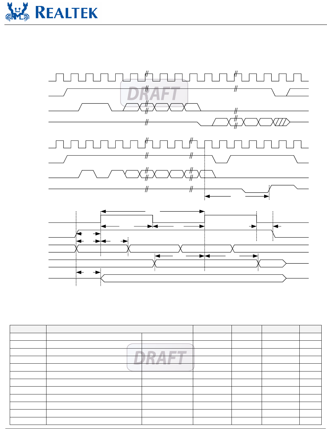
RTL8187SE
Datasheet
Single-Chip Wireless LAN Network Interface Controller
w/PCI Express Interface
42 Track ID: JATR-1076-21 Rev. 1.0
11.3. AC Characteristics
11.3.1. Serial EEPROM Interface Timing
(93C46(64*16)/93C56(128*16))
EESK
EECS
EEDI
EEDO
1 1 0 An A2 A0A1
Dn D1 D0
EESK
(Read)
(Write)
(Read)
(Write)
0
tcs
EESK
EECS
EEDI
EEDO
1 10 An A0 ...
Dn
tcs
... D0
BUSY READY
High Impedance
High Impedance
twp
EECS
EEDI
EEDO
EEDO
(Read)
(Program) STATUS VALID
tsk
tskh tskl
tcss
tdis tdih
tdos tdoh
tcsh
tsv
Figure 6. Serial EEPROM Interface Timing
Table 29. EEPROM Access Timing Parameters
Symbol Parameter Minimum Typical Maximum Units
tcs Minimum CS Low Time 9346/9356 1000/250 - - ns
twp Write Cycle Time 9346/9356 - - 10/10 ms
tsk SK Clock Cycle Time 9346/9356 4/1 - - s
tskh SK High Time 9346/9356 1000/500 - - ns
tskl SK Low Time 9346/9356 1000/250 - - ns
tcss CS Setup Time 9346/9356 200/50 - - ns
tcsh CS Hold Time 9346/9356 0/0 - - ns
tdis DI Setup Time 9346/9356 400/50 - - ns
tdih DI Hold Time 9346/9356 400/100 - - ns
tdos DO Setup Time 9346/9356 2000/500 - - ns
tdoh DO Hold Time 9346/9356 - - 2000/500 ns
tsv CS to Status Valid 9346/9356 - - 1000/500 ns

RTL8187SE
Datasheet
Single-Chip Wireless LAN Network Interface Controller
w/PCI Express Interface
43 Track ID: JATR-1076-21 Rev. 1.0
11.4. PCI Express Bus Parameters
11.4.1. Differential Transmitter Parameters
Table 30. Differential Transmitter Parameters
Symbol Parameter Min Typical Max Units
UI Unit Interval 399.88 400 400.12 ps
VTX-DIFFp-p Differential Peak to Peak Output Voltage 0.800 - 1.2 V
VTX-DE-RATIO De-Emphasized Differential Output Voltage (Ratio) -3.0 -3.5 -4.0 dB
TTX-EYE Minimum Tx Eye Width 0.75 - - UI
TTX-EYE-MEDIAN-
to-MAX-JITTER
Maximum time between the jitter median and
maximum deviation from the median
- - 0.125 UI
TTX-RISE, TTX-FALL D+/D- Tx Output Rise/Fall Time 0.125 - - UI
VTX-CM-ACp RMS AC Peak Common Mode Output Voltage - - 20 mV
VTX-CM-DCACTIVE-
IDLEDELTA
Absolute Delta of DC Common Mode Voltage During
L0 and Electrical Idle
0 - 100 mV
VTX-CM-DCLINE- DELTA Absolute Delta of DC Common Mode Voltage between
D+ and D-
0 - 25 mV
VTX-IDLE-DIFFp Electrical Idle Differential Peak Output Voltage 0 - 20 mV
VTX-RCV-DETECT The amount of voltage change allowed during
Receiver Detection
- - 600 mV
VTX-DC-CM The TX DC Common Mode Voltage 0 - 3.6 V
ITX-SHORT TX Short Circuit Current Limit - - 90 mA
TTX-IDLE-MIN Minimum Time Spent in Electrical Idle 50 - - UI
TTX-IDLE- SETTO-IDLE Maximum time to transition to a valid Electrical Idle
after sending an Electrical Idle ordered set
- - 20 UI
TTX-IDLE-TOTO-
DIFF-DATA
Maximum time to transition to valid TX specifications
after leaving an Electrical Idle condition
- - 20 UI
RLTX-DIFF Differential Return Loss 10 - - dB
RLTX-CM Common Mode Return Loss 6 - - dB
ZTX-DIFF-DC DC Differential TX Impedance 80 100 120
LTX-SKEW Lane-to-Lane Output Skew - - 500+2UI ps
CTX AC Coupling Capacitor 75 - 200 nF
Tcrosslink Crosslink Random Timeout 0 - 1 ms
Note1: Refer to PCI Express Base Specification, rev.1.1, for correct measurement environment setting of each parameter.
Note2: The data rate can be modulated with an SSC (Spread Spectrum Clock) from +0 to -0.5% of the nominal data rate
frequency, at a modulation rate in the range not exceeding 30 kHz – 33 kHz. The +/- 300 ppm requirement still holds, which
requires the two communicating ports be modulated such that they never exceed a total of 600 ppm difference.

RTL8187SE
Datasheet
Single-Chip Wireless LAN Network Interface Controller
w/PCI Express Interface
44 Track ID: JATR-1076-21 Rev. 1.0
11.4.2. Differential Receiver Parameters
Table 31. Differential Receiver Parameters
Symbol Parameter Min. Typical Max. Units
UI Unit Interval 399.88 400 400.12 ps
VRX-DIFFp-p Differential Input Peak to Peak Voltage 0.175 - 1.200 V
TRX-EYE Minimum Receiver Eye Width 0.4 - - UI
TRX-EYE-MEDIAN-to-
MAX-JITTER
Maximum time between the jitter median and maximum
deviation from the median
- - 0.3 UI
VRX-CM-ACp AC Peak Common Mode Input Voltage - - 150 mV
RLRX-DIFF Differential Return Loss 10 - - dB
RLRX-CM Common Mode Return Loss 6 - - dB
ZRX-DIFF-DC DC Differential Input Impedance 80 100 120
ZRX--DC DC Input Impedance 40 50 60
ZRX-HIGH-IMP-DC Powered Down DC Input Impedance 200k - -
VRX-IDLE-DET-DIFFp-p Electrical Idle Detect Threshold 65 - 175 mV
TRX-IDLE-DET-
DIFFENTERTIME
Unexpected Electrical Idle Enter Detect Threshold
Integration Time
- - 10 ms
LRX-SKEW Total Skew - - 20 ns
Note: Refer to PCI Express Base Specification, rev.1.1, for correct measurement environment setting of each parameter.
11.4.3. REFCLK Parameters
Table 32. REFCLK Parameters
Symbol Parameter 100MHz Input
Min Max
Units Note
Rise Edge Rate Rising Edge Rate 0.6 4.0 V/ns 2, 3
Fall Edge Rate Falling Edge Rate 0.6 4.0 V/ns 2, 3
VIH Differential Input High Voltage +150 - mV 2
VIL Differential Input Low Voltage - -150 mV 2
VCROSS Absolute Crossing Point Voltage +250 +550 mV 1, 4, 5
VCROSS DELTA Variation of VCROSS Over All Rising
Clock Edges
- +140 mV 1, 4, 9
VRB Ring-Back Voltage Margin -100 +100 mV 2, 12
TSTABLE Time before VRB is Allowed 500 - ps 2, 12
TPERIOD AVG Average Clock Period Accuracy -300 +2800 ppm 2, 10, 13
TPERIOD ABS Absolute Period (Including Jitter and
Spread Spectrum)
9.847 10.203 ns 2, 6
TCCJITTER Cycle to Cycle Jitter -150 ps 2
VMAX Absolute Max Input Voltage - +1.15 V 1, 7
VMIN Absolute Min Input Voltage - -0.3 V 1, 8
Duty Cycle Duty Cycle 40 60 % 2

RTL8187SE
Datasheet
Single-Chip Wireless LAN Network Interface Controller
w/PCI Express Interface
45 Track ID: JATR-1076-21 Rev. 1.0
Symbol Parameter 100MHz Input
Min Max
Units Note
Rise-Fall Matching Rising edge rate (REFCLK+) to falling
edge rate (REFCLK-) matching
- 20 % 1, 14
ZC-DC Clock Source DC Impedance 40 60 1, 11
Note1: Measurement taken from single ended waveform.
Note2: Measurement taken from differential waveform.
Note3: Measured from -150 mV to +150 mV on the differential waveform (derived from REFCLK+ minus REFCLK-). The
signal must be monotonic through the measurement region for rise and fall time. The 300 mV measurement window is
centered on the differential zero crossing.
Note4: Measured at crossing point where the instantaneous voltage value of the rising edge of REFCLK+ equals the falling
edge of REFCLK-.
Note5: Refers to the total variation from the lowest crossing point to the highest, regardless of which edge is crossing.
Refers to all crossing points for this measurement.
Note6: Defines as the absolute minimum or maximum instantaneous period. This includes cycle to cycle jitter, relative PPM
tolerance, and spread spectrum modulation.
Note7: Defined as the maximum instantaneous voltage including overshoot.
Note8: Defined as the minimum instantaneous voltage including undershoot.
Note9: Defined as the total variation of all crossing voltages of Rising REFCLK+ and Falling REFCLK-. This is the
maximum allowed variance in VCROSS for any particular system.
Note10: Refer to Section 4.3.2.1 of the PCI Express Base Specification, Revision 1.1 for information regarding PPM
considerations.
Note11: System board compliance measurements must use the test load card described in Figure16. REFCLK+ and
REFCLK- are to be measured at the load capacitors CL. Single ended probes must be used for measurements requiring
single ended measurements. Either single ended probes with math or differential probe can be used for differential
measurements. Test load CL = 2 pF.
Note12: TSTABLE is the time the differential clock must maintain a minimum ±150 mV differential voltage after rising/falling
edges before it is allowed to droop back into the VRB ±100 mV differential range. See Figure 15.
Note13: PPM refers to parts per million and is a DC absolute period accuracy specification. 1 PPM is 1/1,000,000th of
100.000000 MHz exactly or 100 Hz. For 300 PPM then we have a error budget of 100 Hz/PPM * 300 PPM = 30 kHz. The
period is to be measured with a frequency counter with measurement window set to 100 ms or greater. The ±300 PPM
applies to systems that do not employ Spread Spectrum or that use common clock source. For systems employing Spread
Spectrum there is an additional 2500 PPM nominal shift in maximum period resulting from the 0.5% down spread resulting
in a maximum average period specification of +2800 PPM
Note14: Matching applies to rising edge rate for REFCLK+ and falling edge rate for REFCLK-. It is measured using a ±75
mV window centered on the median cross point where REFCLK+ rising meets REFCLK- falling. The median cross point is
used to calculate the voltage thresholds the oscilloscope is to use for the edge rate calculations. The Rise Edge Rate of
REFCLK+ should be compared to the Fall Edge Rate of REFCLK-, the maximum allowed difference should not exceed
20% of the slowest edge rate.
Note15: Refer to PCI Express Card Electromechanical Specification, rev.1.1, for correct measurement environment setting
of each parameter.
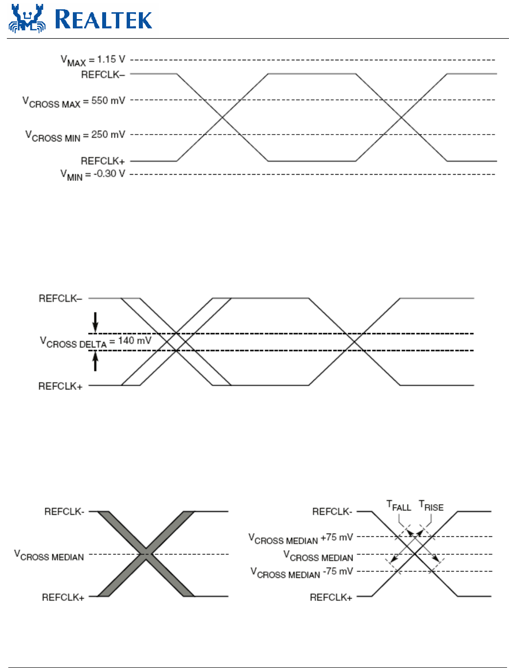
RTL8187SE
Datasheet
Single-Chip Wireless LAN Network Interface Controller
w/PCI Express Interface
46 Track ID: JATR-1076-21 Rev. 1.0
Figure 7. Single-Ended Measurement Points for Absolute Cross Point and Swing
Figure 8. Single-Ended Measurement Points for Delta Cross Point
Figure 9. Single-Ended Measurement Points for Rise and Fall Time Matching
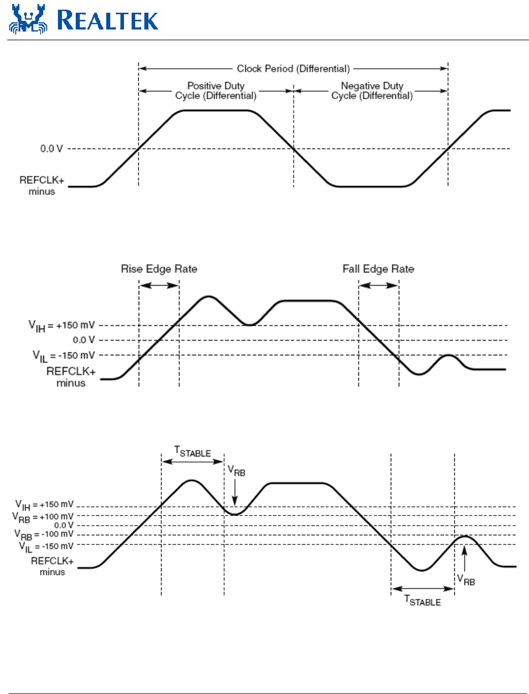
RTL8187SE
Datasheet
Single-Chip Wireless LAN Network Interface Controller
w/PCI Express Interface
47 Track ID: JATR-1076-21 Rev. 1.0
Figure 10. Differential Measurement Points for Duty Cycle and Period
Figure 11. Differential Measurement Points for Rise and Fall Time
Figure 12. Differential Measurement Points for Ringback
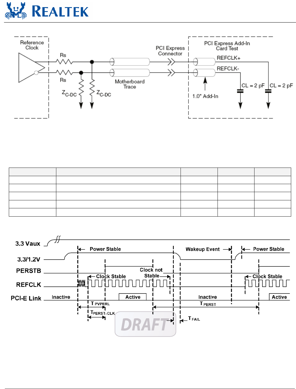
RTL8187SE
Datasheet
Single-Chip Wireless LAN Network Interface Controller
w/PCI Express Interface
48 Track ID: JATR-1076-21 Rev. 1.0
Figure 13. Reference Clock System Measurement Point and Loading
11.4.4. Auxiliary Signal Timing Parameters
Table 33. Auxiliary Signal Timing Parameters
Symbol Parameter Min Max Units
TPVPERL Power Stable to PERSTB Inactive 100 - ms
TPERST-CLK REFCLK Stable before PERSTB Inactive 100 - µs
TPERST PERSTB Active Time 100 - µs
TFAIL Power Level Invalid to PWRGD Inactive - 500 ns
TWKRF LANWAKEB Rise/Fall Time - 100 ns
Figure 14. Auxiliary Signal Timing
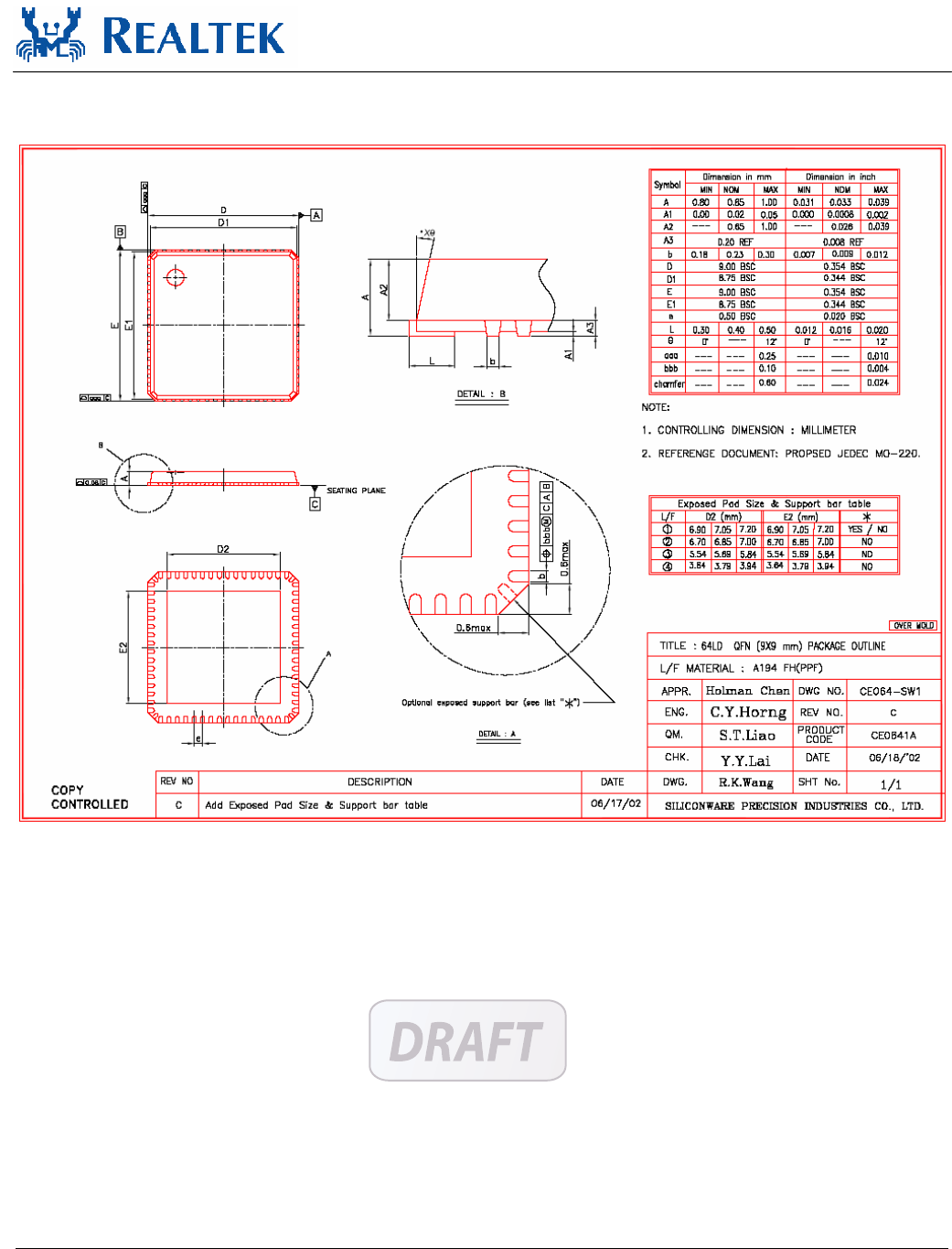
RTL8187SE
Datasheet
Single-Chip Wireless LAN Network Interface Controller
w/PCI Express Interface
49 Track ID: JATR-1076-21 Rev. 1.0
12. Mechanical Dimensions
Note: The RTL8187SE Exposed Pad Size is type 3.

RTL8187SE
Datasheet
Single-Chip Wireless LAN Network Interface Controller
w/PCI Express Interface
50 Track ID: JATR-1076-21 Rev. 1.0
13. Ordering Information
Table 34. Ordering Information
Part Number Package Status
RTL8187SE-GR 64-Pin E-pad QFN with Green Package Production
Note: See page 7 for Green package identification.
Realtek Semiconductor Corp.
HeadqµArters
No. 2, Innovation Road II, Hsinchu Science Park,
Hsinchu 300, Taiwan.
Tel: 886-3-5780211 Fax: 886-3-5776047
www.realtek.com.tw
Federal Communication Commission Interference Statement This equipment has been tested and found to comply with the limits for a Class B digital device, pursuant to
Part 15 of the FCC Rules. These limits are designed to provide reasonable protection against harmful interference in a residential installation. This equipment generates,
uses and can radiate radio frequency energy and, if not installed and used in accordance with the instructions, may cause harmful interference to radio communications.
However, there is no guarantee that interference will not occur in a particular installation. If this equipment does cause harmful interference to radio or television reception,
which can be determined by turning the equipment off and on, the user is encouraged to try to correct the interference by one of the following measures:
Reorient or relocate the receiving antenna.
Increase the separation between the equipment and receiver.
Connect the equipment into an outlet on a circuit different from that to which the receiver is connected.
Consult the dealer or an experienced radio/TV technician for help.
For product available in the USA/Canada market, only channel 1~11 can be operated. Selection of other channels is not possible. This device and its antenna(s) must not
be co-located or operation in conjunction with any other antenna or transmitter. FCC Radiation Exposure Statement: This equipment complies with FCC radiation exposure
limits set forth for an uncontrolled environment. This equipment should be installed and operated with minimum distance 20cm between the radiator & your body.
IMPORTANT NOTE: This module is intended for OEM integrator. The OEM integrator is still responsible for the FCC compliance requirement of the end
product, which integrates this module. 20cm minimum distance has to be able to be maintained between the antenna and the users for the host this module
is integrated into. Under such configuration, the FCC radiation exposure limits set forth for an population/uncontrolled environment can be satisfied. Any
changes or modifications not expressly approved by the manufacturer could void the user's authority to operate this equipment. USERS MANUAL OF THE
END PRODUCT: In the users manual of the end product, the end user has to be informed to keep at least 20cm separation with the antenna while this end
product is installed and operated. The end user has to be informed that the FCC radio-frequency exposure guidelines for an uncontrolled environment can
be satisfied. The end user has to also be informed that any changes or modifications not expressly approved by the manufacturer could void the user's
authority to operate this equipment. If the size of the end product is smaller than 8x10cm, then additional FCC part 15.19 statement is required to be
available in the users manual: This device complies with Part 15 of FCC rules. Operation is subject to the following two conditions: (1) this device may not
cause harmful interference and (2) this device must accept any interference received, including interference that may cause undesired operation. LABEL
OF THE END PRODUCT: The final end product must be labeled in a visible area with the following " Contains TX FCC ID: TX2-RTL8187SE ". If the size of
the end product is larger than 8x10cm, then the following FCC part 15.19 statement has to also be available on the label: This device complies with Part
15 of FCC rules. Operation is subject to the following two conditions: (1) this device may not cause harmful interference and (2) this device must accept any
interference received, including interference that may cause undesired operation.
This Class B digital apparatus complies with Canadian ICES-003. Cet appareil numérique de la classe B conforme á la norme NMB-003 du Canada.
Operation is subject to the following two conditions: (1) this device may not cause interference, and (2) this device must accept any interference, including interference that
may cause undesired operation of the device. For product available in the USA/Canada market, only channel 1~11 can be operated. Selection of other channels is not
possible. This device and its antenna(s) must not be co-located or operation in conjunction with any other antenna or transmitter.To reduce potential radio interference to
other users, the antenna type and its gain should be so chosen that the equivalent isotropically radiated power (e.i.r.p) is not more than that permitted for successful
communication. IC Radiation Exposure Statement: This equipment complies with IC RSS-102 radiation exposure limits set forth for an uncontrolled environment. This
equipment should be installed and operated with minimum distance 20cm between the radiator & your body.
IMPORTANT NOTE: This module is intended for OEM integrator. The OEM integrator is still responsible for the IC compliance requirement of the end product, which integrates this
module. 20cm minimum distance has to be able to be maintained between the antenna and the users for the host this module is integrated into. Under such configuration, the IC
RSS-102 radiation exposure limits set forth for an population/uncontrolled environment can be satisfied. Any changes or modifications not expressly approved by the manufacturer could
void the user's authority to operate this equipment. USERS MANUAL OF THE END PRODUCT: In the users manual of the end product, the end user has to be informed to keep at least
20cm separation with the antenna while this end product is installed and operated. The end user has to be informed that the IC radio-frequency exposure guidelines for an uncontrolled
environment can be satisfied. The end user has to also be informed that any changes or modifications not expressly approved by the manufacturer could void the user's authority to
operate this equipment. IC statement is required to be available in the users manual: This Class B digital apparatus complies with Canadian ICES-003. Operation is subject to the
following two conditions: (1) this device may not cause harmful interference and (2) this device must accept any interference received, including interference that may cause undesired
operation. LABEL OF THE END PRODUCT: The final end product must be labeled in a visible area with the following " Contains TX IC : 6317A-RTL8187SE".
Hereby, Realtek, declares that this device is in compliance with the essential requirement and other relevant provisions of the R&TTE Driective 1999/5/EC. This device will
be sold in the following EEA countries:Austria, Italy, Belgium, Liechtenstein, Denmark, Luxembourg, Finland, Netherlands, France, Norway, Germany, Portugal, Greece,
Spain, Iceland, Sweden, Ireland, United Kingdom, Cyprus, Czech Republic, Estonia, Hungary, Latvia, Lithuania, Malta, Slovakia, Poland, Slovenia Bulgaria, Romania.
Any changes or modifications not expressly approved by the party responsible for compliance could void the user’s authority to operate this equipment.