Realtek Semiconductor RTL8192EHMC 802.11 b/g/n RTL8192E half miniCard User Manual User s manual for FCC
Realtek Semiconductor Corp. 802.11 b/g/n RTL8192E half miniCard User s manual for FCC
UserManual.wiki
>
Realtek Semiconductor
>
RTL8192EHMC User Manual
>
Manual
Contents
1.
Manual
2.
Users Manual
3.
User manual 1 of 3
4.
User manual 2 of 3
5.
User manual 3 of 3
Manual
Navigation menu
Upload a User Manual
Namespaces
Wiki Guide
HTML
PDF
Info
Views
User Manual
Discussion / Help
Navigation
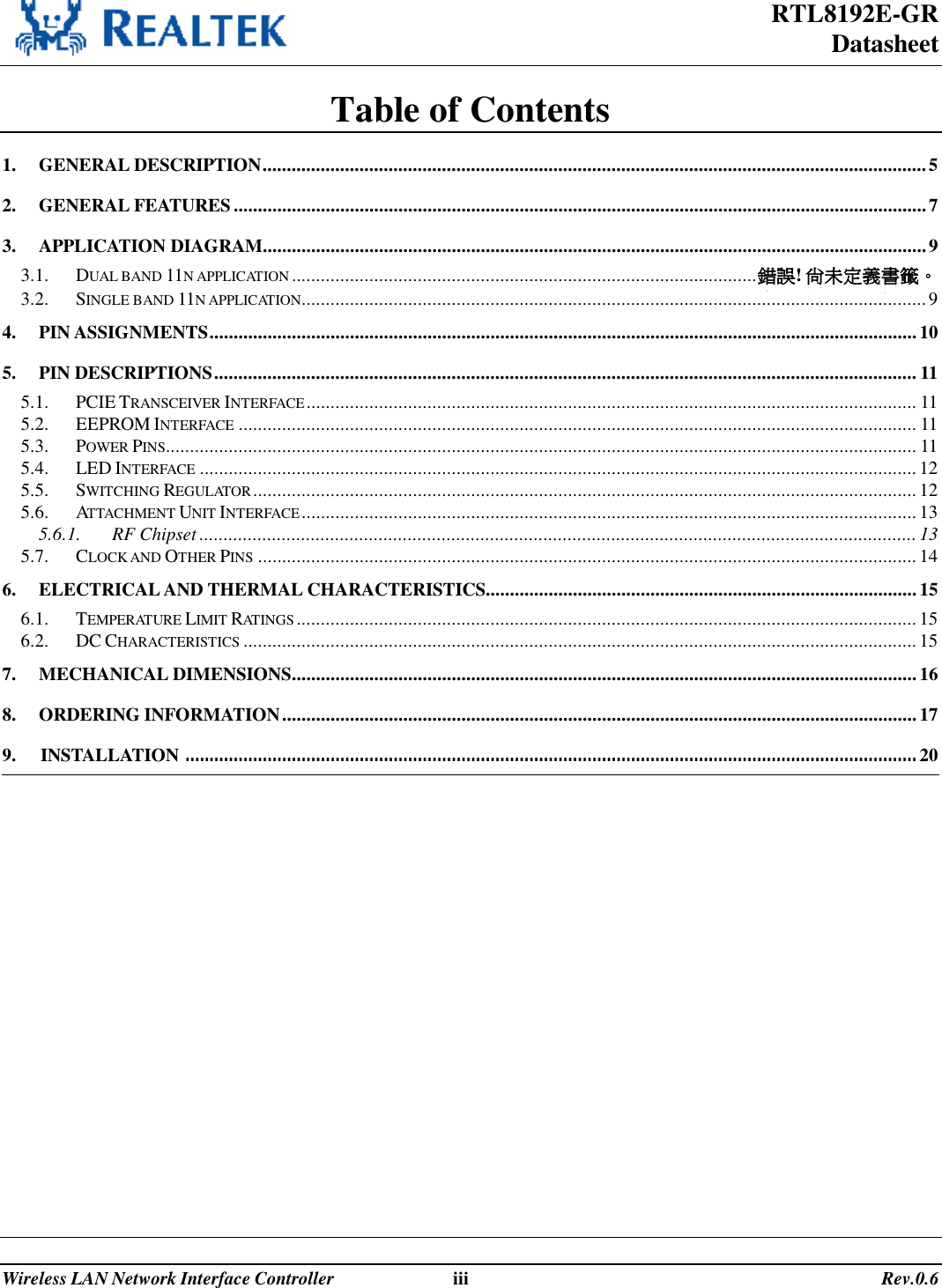
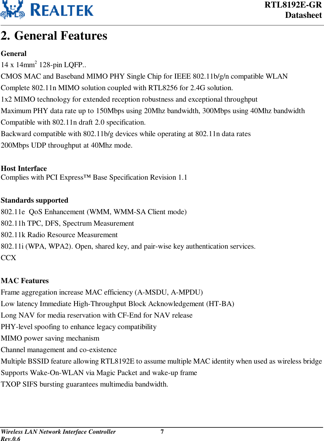
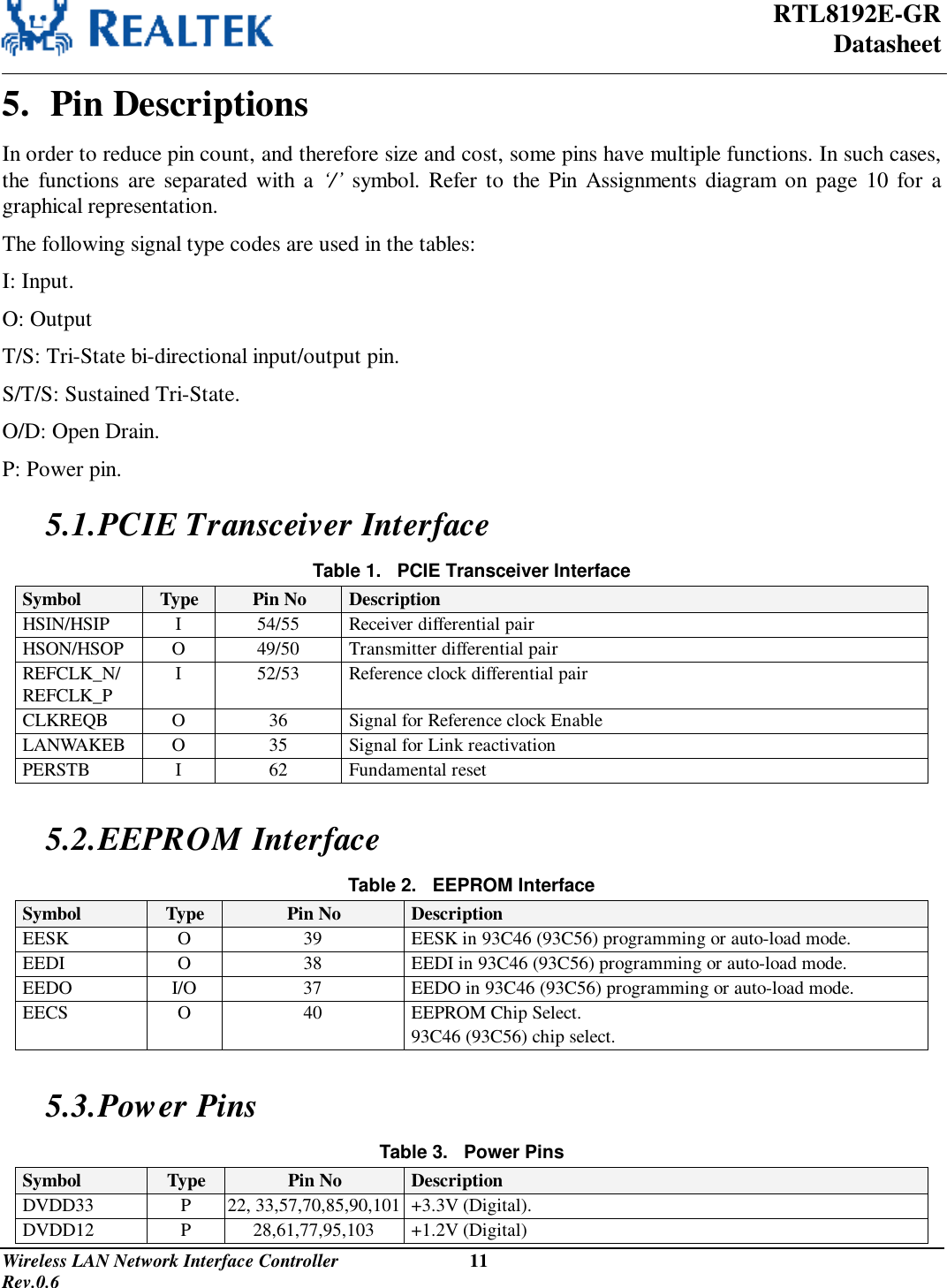
![RTL8192E-GR Datasheet Wireless LAN Network Interface Controller 10 Rev.0.6 4. Pin Assignments .129 GNDRTL8192ELLLLLLLTXXXV TAIWAN33 DVDD3360 DGND1259 ISOLATEBPIN58 EXPWRONPIN57 DVDD3356 DGND3355 HSIP54 HSIN53 REFCLK-P52 REFCLK-M51 EVDD1250 HSOP49 HSON48 EGND47 RREF46 DV1245 AGND44 AV3343 AGND42 PCIESELPIN41 EXRSTBPIN40 EECSPIN39 EESKPIN38 EEDIPIN37 EEDOPIN36 CLKREQBPIN35 LANWAKBPIN34 DGND3361 DVDD1263 DGND3362 PERSTBPIN64 HG1128 VDDBG101 DVDD33102 DGND33103 DVDD12104 DGND12105 VDDREG106 VDDPLL107 REFCKP108 REFCKN109 CNDPLL110 VDD15111 GND15112 DA60113 TSSI5G-2114 TSSI2G-2115 TSSI-2116 RIN-2117 RIP-2118 VDDA119 RQP-2120 RQN-2121 GNDA122 TIN-2123 TIP-2124 TQP-2125 TQN-2126 TQN-3127 TQP-3100 B-RFLEPIN98 B-RFSDPIN99 A-RFLEPIN97 A-RFSDPIN17 GNDPLL32 B-TRSWPIN31 B-TRSWBPIN30 B-PAPE-5GPIN29 B-PAPE-2GPIN28 DVDD1227 DGND1226 A-TRSWPIN25 A-TRSWBPIN24 A-PAPE-5GPIN23 A-PAPE-2GPIN22 DVDD3321 DGND3320 XO19 XI18 VDD3316 VDDPLL1 R15K2 GNDBG3 GNDA5 TIN-36 VDDA7 RQN-38 RQP-39 VDDA10 RIP-311 RIN-312 TSSI2G-313 TSSI5G-314 RSSI-315 GNDA65 REG-OUT180 HG279 ENSWREG1-H78 GPIO[3]77 DVDD1276 DGND1275 GPIO[2]74 GPIO[1]73 GPIO[0]72 LED[1]71 LED[0]70 DVDD3369 DGND3368 RSET67 HV166 HV196 DCND1281 REG-OUT282 HV283 HV284 DGND3385 DVDD3386 GPIO[4]87 GPIO[5]88 GPIO[6]89 GPIO[7]90 DVDD3391 DGND3392 A-RFENVPIN93 ARFRWPIN94 A-RFSCKPIN95 DVDD124 TIP-3 Figure 2. Pin Assignments](https://usermanual.wiki/Realtek-Semiconductor/RTL8192EHMC.Manual/User-Guide-1025264-Page-10.png)