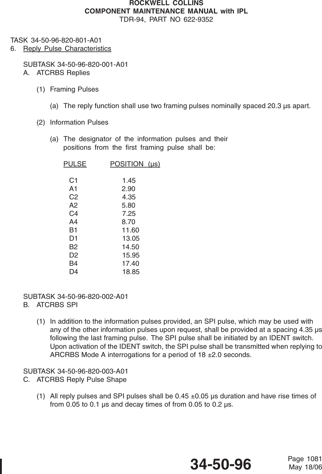
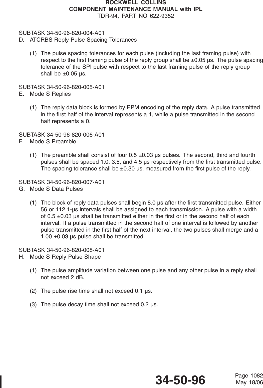
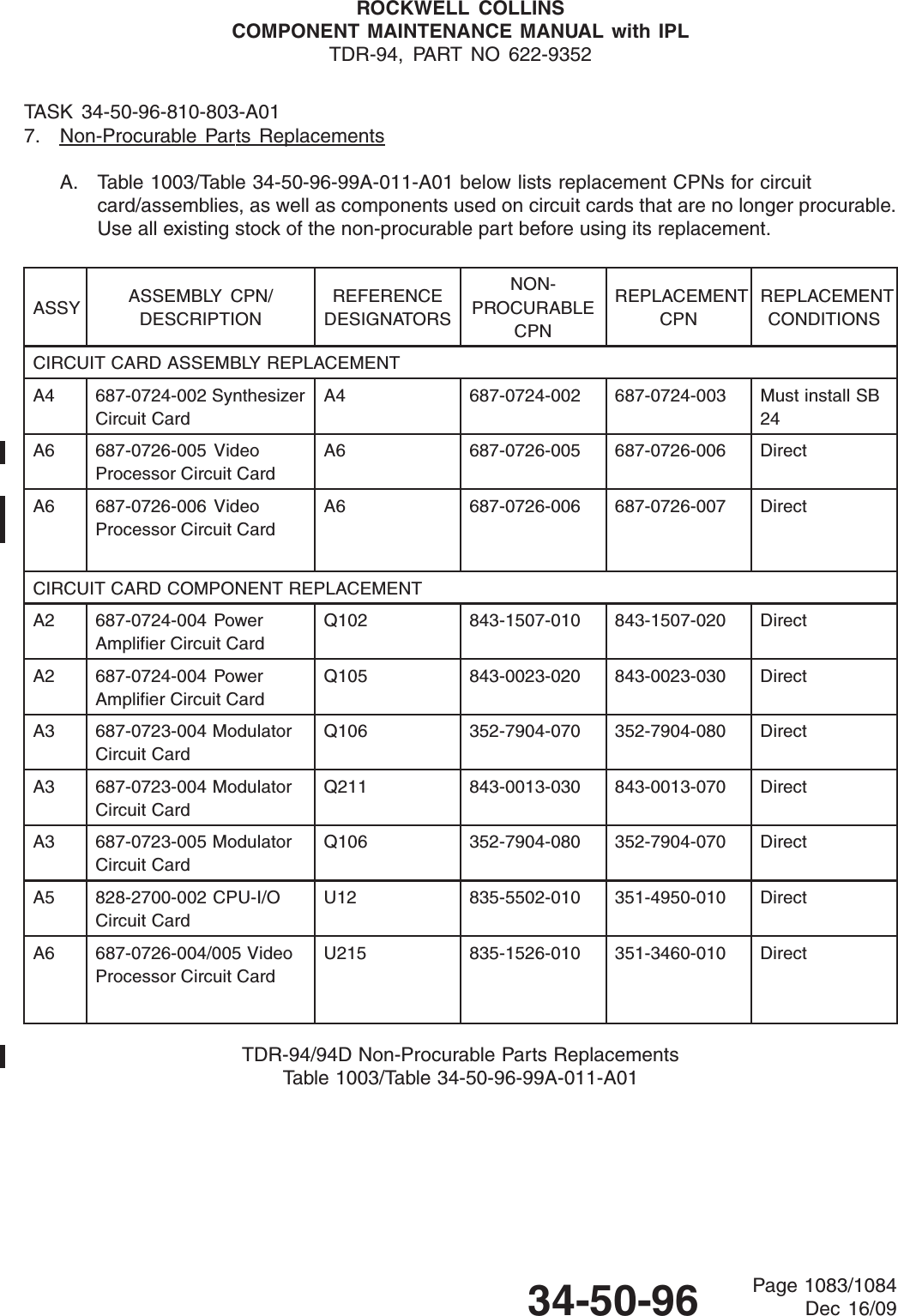
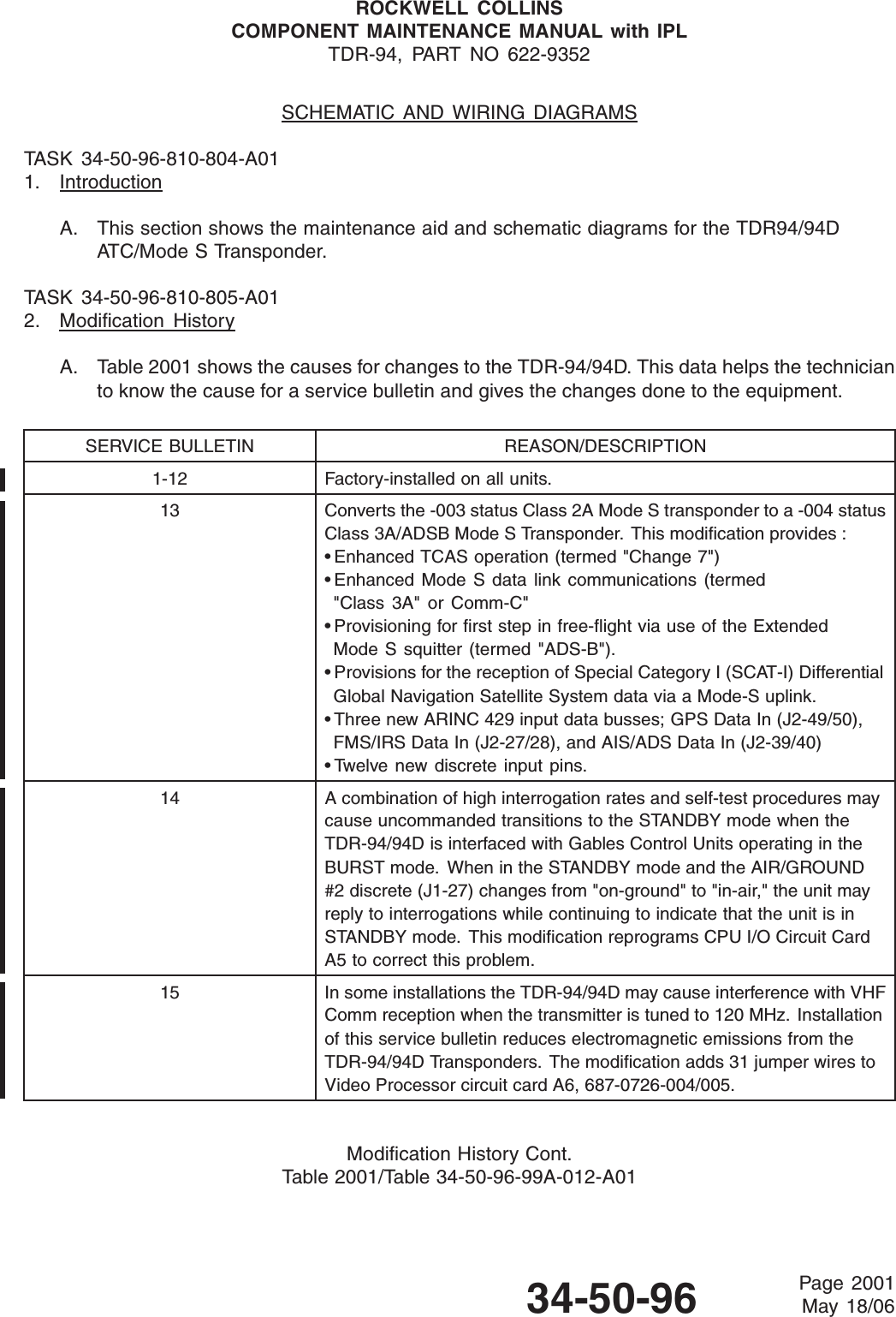
Rockwell Collins 6229210 TRANSPONDER User Manual P2
Rockwell Collins Inc TRANSPONDER P2
UserManual.wiki
>
Rockwell Collins
>
6229210 User Manual
>
User Manual P2
Contents
1.
User Manual P1
2.
User Manual P2
3.
User Manual P3 1
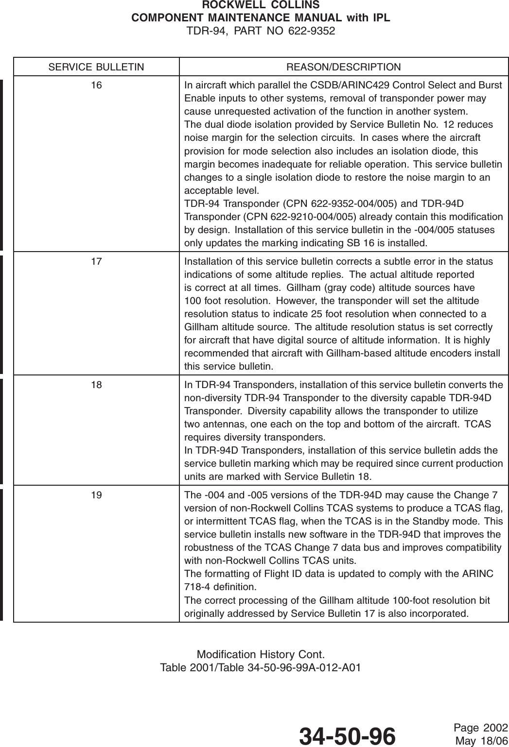
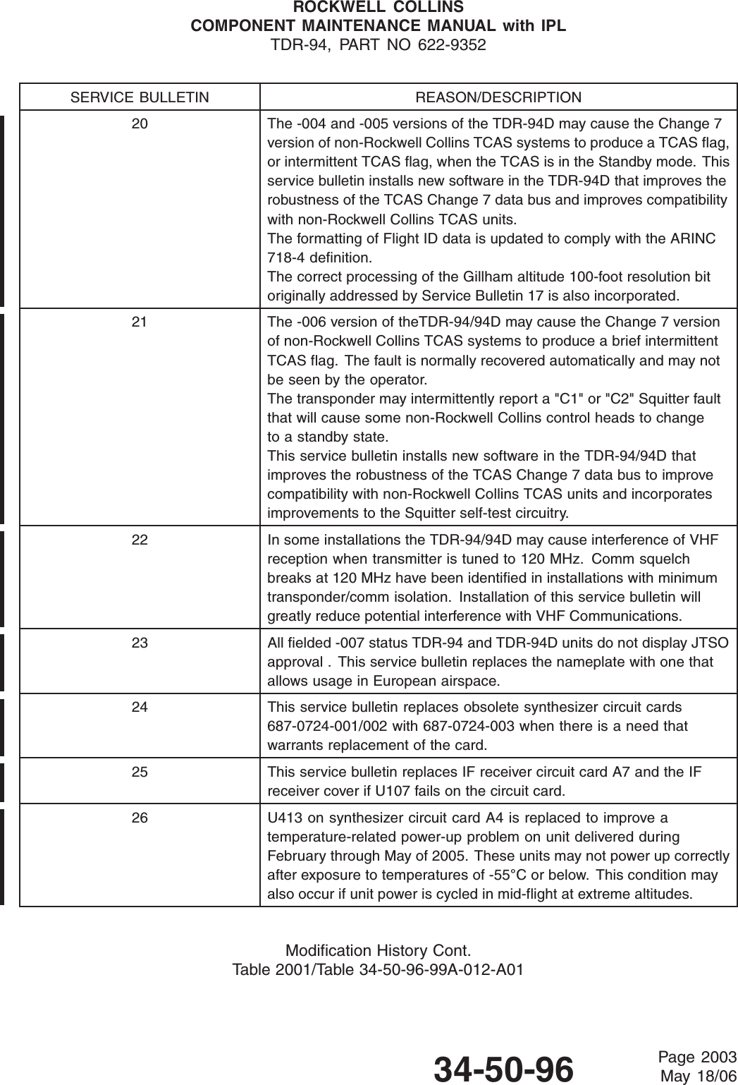
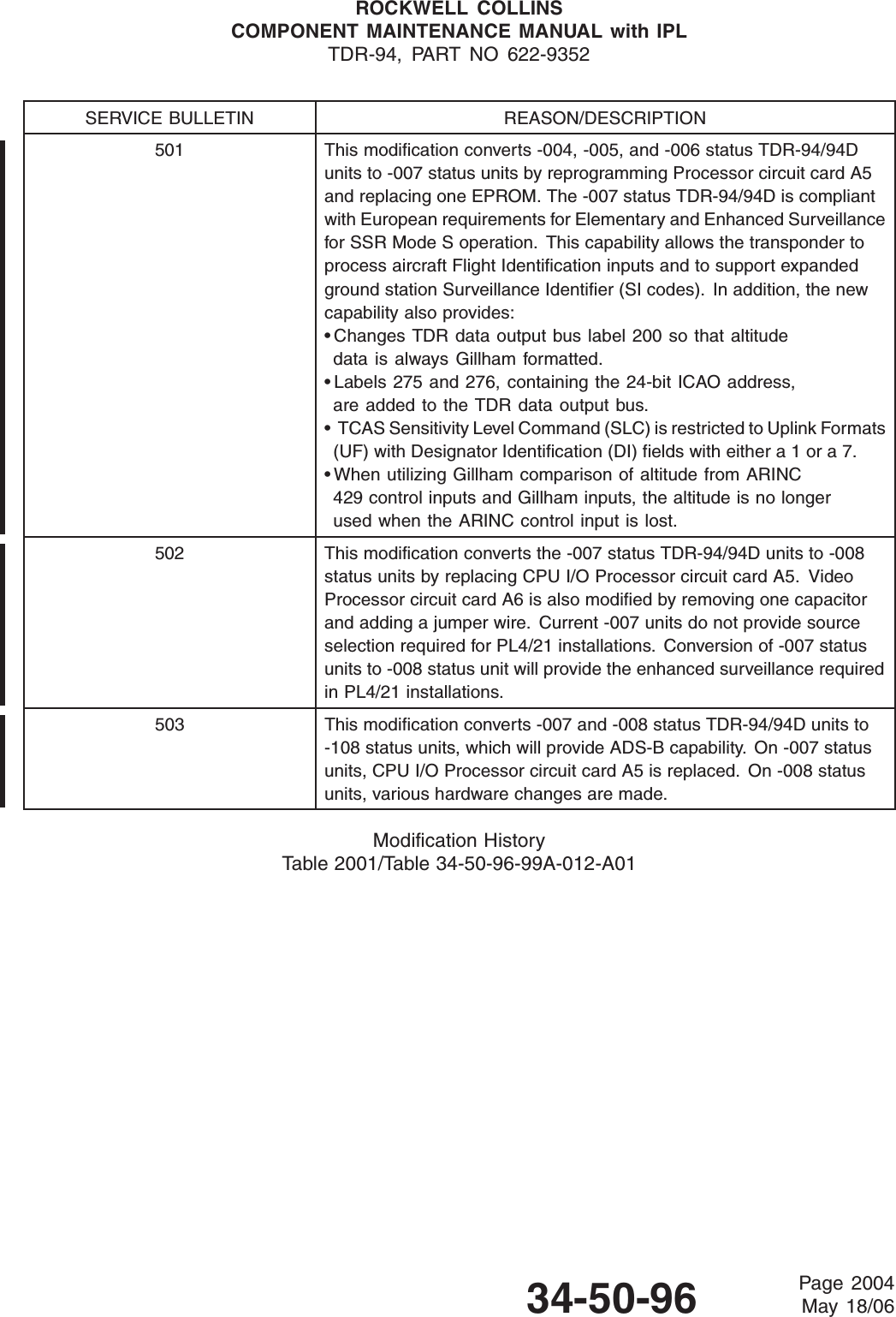
4.
User Manual P3 2
5.
User Manual P4
6.
User Manual P5
7.
User Manual P6
User Manual P2
Navigation menu
Upload a User Manual
Namespaces
Wiki Guide
HTML
PDF
Info
Views
User Manual
Discussion / Help
Navigation