Rockwell Collins 6229210 TRANSPONDER User Manual P2
Rockwell Collins Inc TRANSPONDER P2
Contents
User Manual P2
ROCKWELL COLLINS
COMPONENT MAINTENANCE MANUAL with IPL
TDR-94, PART NO 622-9352
STEP PROCEDURE DESIRED RESULTS
1.21 Verify that no fault codes are indicated on the monitor in either the
"F3" CSDB output word or in the "350" ARINC-429 Maintenance
Data Output word.
1.22 If the UUT fails the Mode-S_Only reply rate as specified in
Table 1001/Table 34-50-96-99A-009-A01 step 1.1.A at ambient
or during temperature test, first verify the DPSK alignment. If
alignment is satisfactory but UUT still fails Table 1001/Table
34-50-96-99A-009-A01 step 1.1.A, replace A7R430 with another
value from the test select listing as shown in the associated parts
list. Reverify DPSK alignment and complete temperature testing
as required.
1.23 After alignment is complete, remove all power from test equipment
and reassemble unit under test.
2.0 Receiver IF/LVPS Assembly, Alignment for CPN 687-0727-005 or subsequent.
2.1 Monitor the 5 VDC output (J7-26) with a DVM while adjusting
A7R507 on the IF/Power Supply board.
5 VDC output adjusted to
4.99 to 5.01 Vdc.
2.2 Monitor J7-33 on the Video Processor board with an oscilloscope.
2.3 Set the MODE-S Test Set to generate ATCRBS MODE-C
interrogations and apply to the bottom antenna connector. Set the
interrogation rate to 450/second.
2.4 a. Set the MODE-S Test Set signal strength for -79 dBm.
b. Adjust A7R196 to the fully clock-wise position. Monitor the
Bottom Video signal at pin 33 of A6P22 with an oscilloscope
while adjusting A7R95.
NOTE: Theoscilloscopemustbesettotheaveraging
mode to properly measure the video pulse at
the low signal levels required.
An observed video level of
0.7 volts Peak.
c. Set the MODE-S test set signal strength to -77 dBm.
d. Monitor the Bottom Video signal at pin 33 of A6P22 while
adjusting A7R196.
An observed video level of
0.7 volts Peak.
e. Verify that the reply rate is between 90% and 100%. If
necessary, readjust A7R195 to the get the desired result.
A reply rate between 90%
and 100%.
2.5 a. Set the MODE-S Test Set signal strength for -31 dBm.
b. Monitor the P1 pulse at J7-33 with a DVM whiling adjusting
A7R179 on the IF-Receiver.
The P1 pulse adjusted to 4.99
to 5.01 V dc.
Alignment Procedure Cont.
Table 1002/Table 34-50-96-99A-010-A01
34-50-96 Page 1077
Apr 17/07

ROCKWELL COLLINS
COMPONENT MAINTENANCE MANUAL with IPL
TDR-94, PART NO 622-9352
STEP PROCEDURE DESIRED RESULTS
2.6 Repeat steps 2.4 and 2.5 as necessary.
2.7 a. Set the MODE-S Test Set signal strength for -27 dBm.
b. Adjust A6R118 on the Video Processor board while monitoring
the positive end of A6C67 with the oscilloscope.
The observed ditch-slope
waveformresultingfromP1is
16.2±.2μswideatitsbase.
2.8 Steps 2.9 through 2.14 are applicable only to the TDR-94Ds that
use the 687-0727-005 Receiver-IF/LVPS. MODE-C interrogations
are applied only to the UUT top antenna port for these steps.
2.9 a. Set the MODE-S Test Set signal strength for -79 dBm.
b. Adjust A7R195 to the fully clockwise position.
c. Monitor the Top Video signal at pin 31 of A6P22 with the
oscilloscope with adjusting A7R94.
NOTE: Theoscilloscopemustbesettotheaveraging
mode to properly measure the video pulse at
the low signal levels required.
An observed video level of
0.7 volts Peak.
d. Set the MODE-S Test Set signal strength for -77 dBm.
e. Monitor the Top Video signal at pin 31 of A6P22 while adjusting
A7R195
An observed video level of
0.7 volts Peak.
2.10 Verify that the reply rate is between 90% and 100%. If necessary,
readjust A7R94 to the get the desired result.
A reply rate between 90%
and 100%.
2.11 a. Set the MODE-S Test Set signal strength for -31 dBm.
b. Monitor the P1 pulse at J7-31 with a DVM whiling adjusting
A7R178 on the IF-Receiver.
The P1 pulse adjusted to 4.99
to 5.01 V dc.
2.12 Repeat steps 2.10 and 2.11 as necessary.
2.13 a. Set the MODE-S Test Set signal strength for -50 dBm.
b. Measure and record the amplitude or the P1 pulse at J7-31. ______ V
c. Apply the same input signal level to the bottom channel.
d. Measure and record the amplitude or the P1 pulse at J7-33. ______ V
Alignment Procedure Cont.
Table 1002/Table 34-50-96-99A-010-A01
34-50-96 Page 1078
May 18/06

ROCKWELL COLLINS
COMPONENT MAINTENANCE MANUAL with IPL
TDR-94, PART NO 622-9352
STEP PROCEDURE DESIRED RESULTS
2.13
(cont)
e. Verify that the two recorded amplitudes are with .1 V of each
other. If necessary, readjust the higher voltage downward with
A7R178 or A7R179 (whichever is applicable) until the two
voltages are with .1 V of each other.
NOTE: If readjustment of A7R178 or A7R179 was necessary,
then the MTL for the top or bottom channel must
also be readjusted in accordance with step 2.4 or
2.10 (whichever is appropriate).
The difference between the
two recorded voltages is 0 ±
0.1 V.
2.14 a. Set the MODE-S Test Set signal strength for -27 dBm.
b. Adjust A6R117 on the Video Processor board while monitoring
the positive end of A6C59 with the oscilloscope.
The observed ditch-slope
waveform resulting from P1 is
16.2±.2μswideatitsbase.
2.15
NOTE: Use extreme care while making the adjustments in steps
2.15 through 2.17. Make the DPSK trimmer capacitor
adjustments in very small increments. These adjustments
are critical to the performance of the TDR-94/94D.
a. To align the DPSK Demodulator VCO, interrogate the bottom
channel with MODE-S ONLY ALL-CALL interrogations having
a signal strength of -50 dBm.
b. Adjust the interrogation center frequency above 1030 MHz
until the reply rate decreases to 90%. Record this frequency
as the upper limit.
Upper Frequency limit: ____
MHz
c. Adjust the interrogation center frequency below 1030 MHz until
the reply rate decreases to 90%. Record this center frequency
as the lower frequency limit .
Lower Frequency limit: ____
MHz
d. Adjust A7R223 to a level where the upper and lower frequency
limits are equidistant from the 1030 MHz center frequency.
The upper frequency limit
must not be less than 1030.6
MHz and the lower frequency
limit must not be greater than
1029.4 MHz
2.16 a. To align the DPSK 60 MHz BPF interrogate the bottom channel
with MODE-S ONLY ALL-CALL interrogations having a signal
strength of -70 dBm and a center frequency of 1030.0 MHz.
b. Slowly adjust A7C110 while monitoring A7J7-37 with the
oscilloscope.
A7C110 is adjusted for the
cleanest and most square
signal pulses at A7J7-37.
Alignment Procedure Cont.
Table 1002/Table 34-50-96-99A-010-A01
34-50-96 Page 1079
May 18/06

ROCKWELL COLLINS
COMPONENT MAINTENANCE MANUAL with IPL
TDR-94, PART NO 622-9352
STEP PROCEDURE DESIRED RESULTS
2.17 a. Set the MODE-S Test Set for a -50 dBm MODE-S ONLY
ALL-CALL interrogation signal.
b. Inject an interference pulse of 0.80 μs duration at a
carrier frequency of 1030 MHz, that is incoherent with the
interrogation. Set the amplitude of the interference pulse to
-3dB less than the desired signal level.
c. Adjust A7C104 for maximum reply efficiency.
NOTE: DPSK adjustments are interactive. The adjustments in
steps 2.15 thru 2.17 should be checked again before
performing the remaining procedures.
2.18 a. Monitor J7-33 with the oscilloscope.
b. Interrogate the bottom channel with MODE-A and MODE-C
interrogations that have a signal strength of -67 dBm.
c. Measure and record the video amplitude of the P1 observed. P1 video amplitude: _____
d. Turn off all interrogations to the UUT.
e. Enable the self-test function. Then adjust A7R122 until the
P1 video signal at J7-33 is equal to the P1 video amplitude
recorded above.
The P1 video amplitude is
within ±0.2V of the recorded
in step 2.18.c above.
2.19 Verify that no fault codes are indicated in either the ‘F3’ CSDB
output word or the ‘350’ ARINC -429 maintenance data output
word.
2.20 If the UUT fails the Mode-S Only reply rate, as specified in step
1.1.A of Table 1001/Table 34-50-96-99A-009-A01 at ambient or
during temperature test, first verify the DPSK alignment and then
complete temperature testing as necessary.
2.21 After alignment is complete, remove all power from the test
equipment and reassemble the UUT.
Alignment Procedure
Table 1002/Table 34-50-96-99A-010-A01
34-50-96 Page 1080
May 18/06

ROCKWELL COLLINS
COMPONENT MAINTENANCE MANUAL with IPL
TDR-94, PART NO 622-9352
TASK 34-50-96-820-801-A01
6. Reply Pulse Characteristics
SUBTASK 34-50-96-820-001-A01
A. ATCRBS Replies
(1) Framing Pulses
(a) The reply function shall use two framing pulses nominally spaced 20.3 μs apart.
(2) Information Pulses
(a) The designator of the information pulses and their
positions from the first framing pulse shall be:
PULSE POSITION (μs)
C1 1.45
A1 2.90
C2 4.35
A2 5.80
C4 7.25
A4 8.70
B1 11.60
D1 13.05
B2 14.50
D2 15.95
B4 17.40
D4 18.85
SUBTASK 34-50-96-820-002-A01
B. ATCRBS SPI
(1) In addition to the information pulses provided, an SPI pulse, which may be used with
any of the other information pulses upon request, shall be provided at a spacing 4.35 μs
following the last framing pulse. The SPI pulse shall be initiated by an IDENT switch.
Upon activation of the IDENT switch, the SPI pulse shall be transmitted when replying to
ARCRBS Mode A interrogations for a period of 18 ±2.0 seconds.
SUBTASK 34-50-96-820-003-A01
C. ATCRBS Reply Pulse Shape
(1) All reply pulses and SPI pulses shall be 0.45 ±0.05 μs duration and have rise times of
from 0.05 to 0.1 μs and decay times of from 0.05 to 0.2 μs.
34-50-96 Page 1081
May 18/06

ROCKWELL COLLINS
COMPONENT MAINTENANCE MANUAL with IPL
TDR-94, PART NO 622-9352
SUBTASK 34-50-96-820-004-A01
D. ATCRBS Reply Pulse Spacing Tolerances
(1) The pulse spacing tolerances for each pulse (including the last framing pulse) with
respect to the first framing pulse of the reply group shall be ±0.05 μs. The pulse spacing
tolerance of the SPI pulse with respect to the last framing pulse of the reply group
shall be ±0.05 μs.
SUBTASK 34-50-96-820-005-A01
E. Mode S Replies
(1) The reply data block is formed by PPM encoding of the reply data. A pulse transmitted
in the first half of the interval represents a 1, while a pulse transmitted in the second
half represents a 0.
SUBTASK 34-50-96-820-006-A01
F. Mode S Preamble
(1) The preamble shall consist of four 0.5 ±0.03 μs pulses. The second, third and fourth
pulses shall be spaced 1.0, 3.5, and 4.5 μs respectively from the first transmitted pulse.
The spacing tolerance shall be ±0.30 μs, measured from the first pulse of the reply.
SUBTASK 34-50-96-820-007-A01
G. Mode S Data Pulses
(1) The block of reply data pulses shall begin 8.0 μs after the first transmitted pulse. Either
56 or 112 1-μs intervals shall be assigned to each transmission. A pulse with a width
of 0.5 ±0.03 μs shall be transmitted either in the first or in the second half of each
interval. If a pulse transmitted in the second half of one interval is followed by another
pulse transmitted in the first half of the next interval, the two pulses shall merge and a
1.00 ±0.03 μs pulse shall be transmitted.
SUBTASK 34-50-96-820-008-A01
H. Mode S Reply Pulse Shape
(1) The pulse amplitude variation between one pulse and any other pulse in a reply shall
not exceed 2 dB.
(2) The pulse rise time shall not exceed 0.1 μs.
(3) The pulse decay time shall not exceed 0.2 μs.
34-50-96 Page 1082
May 18/06
ROCKWELL COLLINS
COMPONENT MAINTENANCE MANUAL with IPL
TDR-94, PART NO 622-9352
TASK 34-50-96-810-803-A01
7. Non-Procurable Parts Replacements
A. Table 1003/Table 34-50-96-99A-011-A01 below lists replacement CPNs for circuit
card/assemblies, as well as components used on circuit cards that are no longer procurable.
Use all existing stock of the non-procurable part before using its replacement.
ASSY ASSEMBLY CPN/
DESCRIPTION
REFERENCE
DESIGNATORS
NON-
PROCURABLE
CPN
REPLACEMENT
CPN
REPLACEMENT
CONDITIONS
CIRCUIT CARD ASSEMBLY REPLACEMENT
A4 687-0724-002 Synthesizer
Circuit Card
A4 687-0724-002 687-0724-003 Must install SB
24
A6 687-0726-005 Video
Processor Circuit Card
A6 687-0726-005 687-0726-006 Direct
A6 687-0726-006 Video
Processor Circuit Card
A6 687-0726-006 687-0726-007 Direct
CIRCUIT CARD COMPONENT REPLACEMENT
A2 687-0724-004 Power
Amplifier Circuit Card
Q102 843-1507-010 843-1507-020 Direct
A2 687-0724-004 Power
Amplifier Circuit Card
Q105 843-0023-020 843-0023-030 Direct
A3 687-0723-004 Modulator
Circuit Card
Q106 352-7904-070 352-7904-080 Direct
A3 687-0723-004 Modulator
Circuit Card
Q211 843-0013-030 843-0013-070 Direct
A3 687-0723-005 Modulator
Circuit Card
Q106 352-7904-080 352-7904-070 Direct
A5 828-2700-002 CPU-I/O
Circuit Card
U12 835-5502-010 351-4950-010 Direct
A6 687-0726-004/005 Video
Processor Circuit Card
U215 835-1526-010 351-3460-010 Direct
TDR-94/94D Non-Procurable Parts Replacements
Table 1003/Table 34-50-96-99A-011-A01
34-50-96 Page 1083/1084
Dec 16/09

ROCKWELL COLLINS
COMPONENT MAINTENANCE MANUAL with IPL
TDR-94, PART NO 622-9352
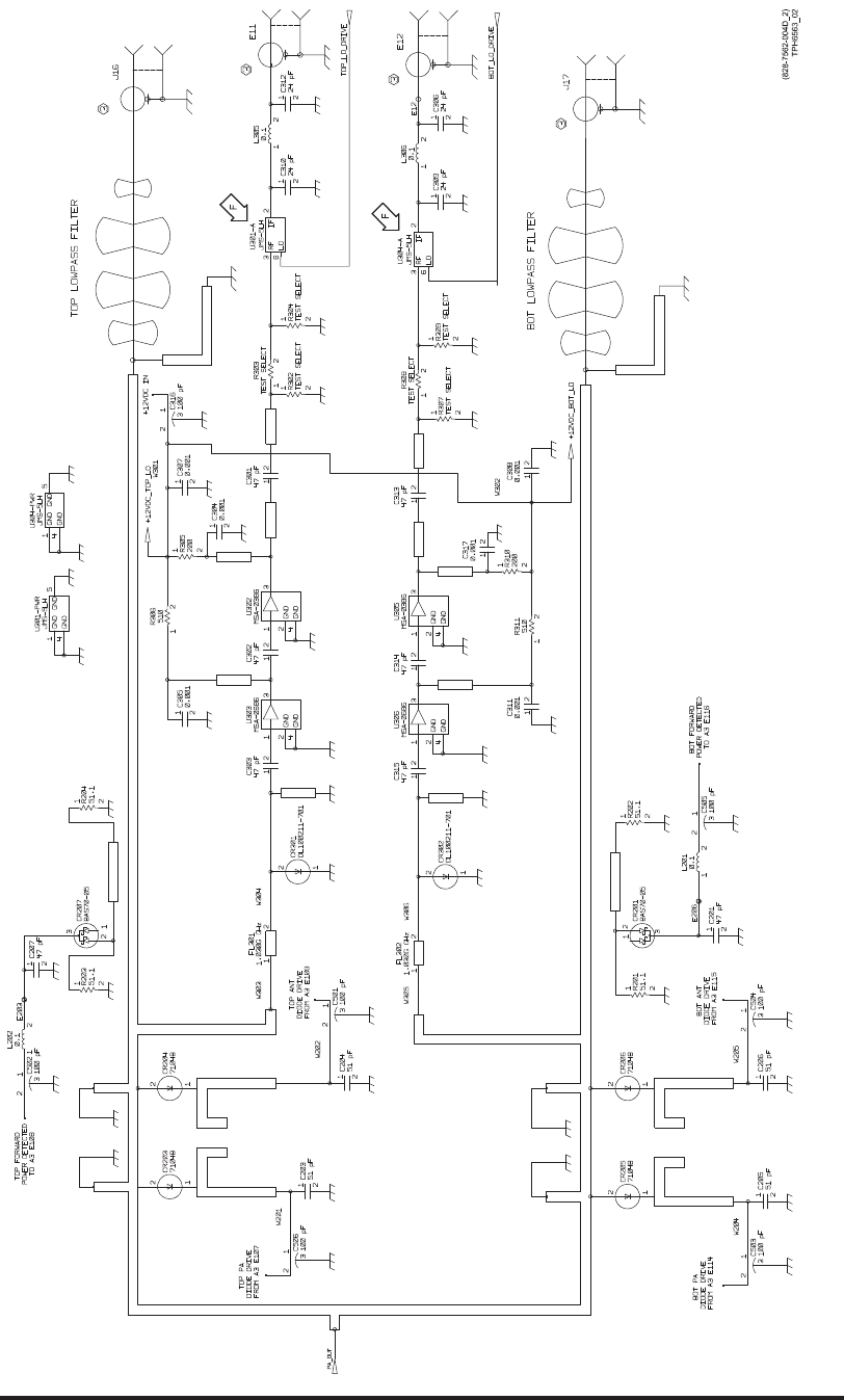
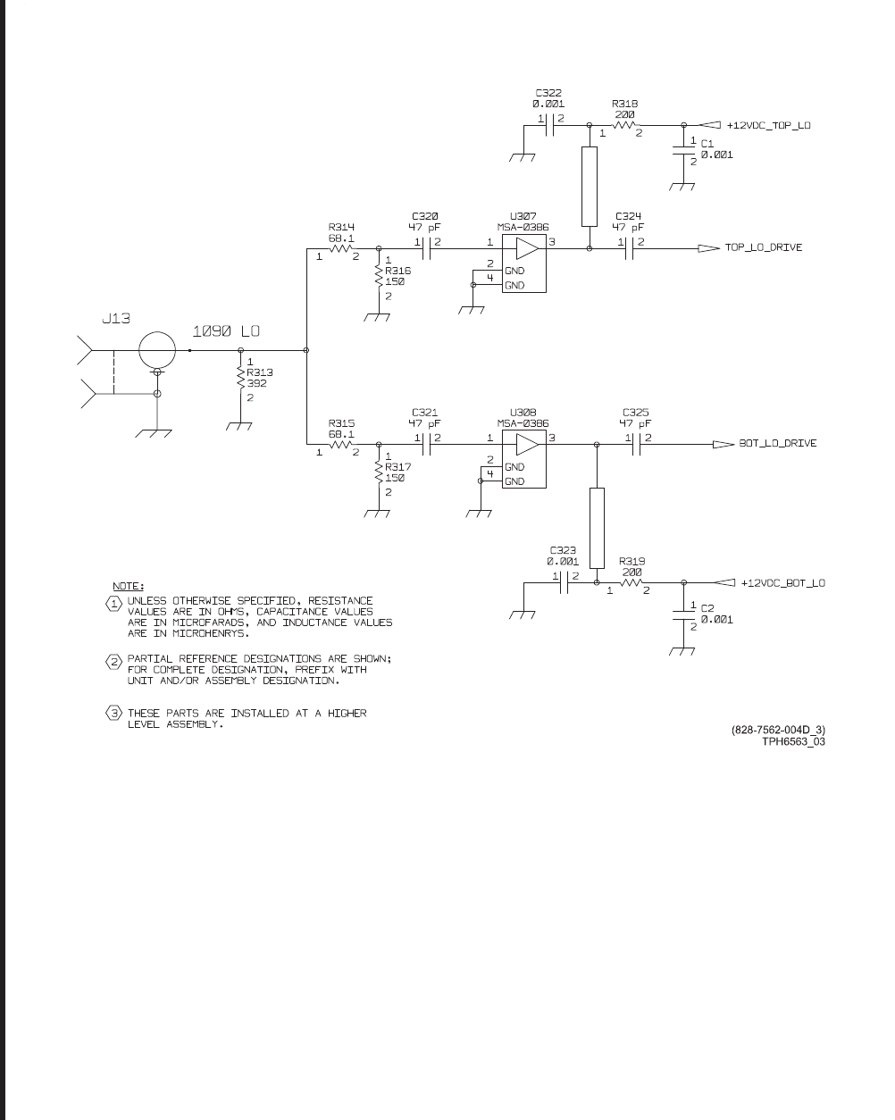
SCHEMATIC AND WIRING DIAGRAMS
TASK 34-50-96-810-804-A01
1. Introduction
A. This section shows the maintenance aid and schematic diagrams for the TDR94/94D
ATC/Mode S Transponder.
TASK 34-50-96-810-805-A01
2. Modification History
A. Table 2001 shows the causes for changes to the TDR-94/94D. This data helps the technician
to know the cause for a service bulletin and gives the changes done to the equipment.
SERVICE BULLETIN REASON/DESCRIPTION
1-12 Factory-installed on all units.
13 Converts the -003 status Class 2A Mode S transponder to a -004 status
Class 3A/ADSB Mode S Transponder. This modification provides :
• Enhanced TCAS operation (termed "Change 7")
• Enhanced Mode S data link communications (termed
"Class 3A" or Comm-C"
• Provisioning for first step in free-flight via use of the Extended
Mode S squitter (termed "ADS-B").
• Provisions for the reception of Special Category I (SCAT-I) Differential
Global Navigation Satellite System data via a Mode-S uplink.
• Three new ARINC 429 input data busses; GPS Data In (J2-49/50),
FMS/IRS Data In (J2-27/28), and AIS/ADS Data In (J2-39/40)
• Twelve new discrete input pins.
14 A combination of high interrogation rates and self-test procedures may
cause uncommanded transitions to the STANDBY mode when the
TDR-94/94D is interfaced with Gables Control Units operating in the
BURST mode. When in the STANDBY mode and the AIR/GROUND
#2 discrete (J1-27) changes from "on-ground" to "in-air," the unit may
reply to interrogations while continuing to indicate that the unit is in
STANDBY mode. This modification reprograms CPU I/O Circuit Card
A5 to correct this problem.
15 In some installations the TDR-94/94D may cause interference with VHF
Comm reception when the transmitter is tuned to 120 MHz. Installation
of this service bulletin reduces electromagnetic emissions from the
TDR-94/94D Transponders. The modification adds 31 jumper wires to
Video Processor circuit card A6, 687-0726-004/005.
Modification History Cont.
Table 2001/Table 34-50-96-99A-012-A01
34-50-96 Page 2001
May 18/06

ROCKWELL COLLINS
COMPONENT MAINTENANCE MANUAL with IPL
TDR-94, PART NO 622-9352
SERVICE BULLETIN REASON/DESCRIPTION
16 In aircraft which parallel the CSDB/ARINC429 Control Select and Burst
Enable inputs to other systems, removal of transponder power may
cause unrequested activation of the function in another system.
The dual diode isolation provided by Service Bulletin No. 12 reduces
noise margin for the selection circuits. In cases where the aircraft
provision for mode selection also includes an isolation diode, this
margin becomes inadequate for reliable operation. This service bulletin
changes to a single isolation diode to restore the noise margin to an
acceptable level.
TDR-94 Transponder (CPN 622-9352-004/005) and TDR-94D
Transponder (CPN 622-9210-004/005) already contain this modification
by design. Installation of this service bulletin in the -004/005 statuses
only updates the marking indicating SB 16 is installed.
17 Installation of this service bulletin corrects a subtle error in the status
indications of some altitude replies. The actual altitude reported
is correct at all times. Gillham (gray code) altitude sources have
100 foot resolution. However, the transponder will set the altitude
resolution status to indicate 25 foot resolution when connected to a
Gillham altitude source. The altitude resolution status is set correctly
for aircraft that have digital source of altitude information. It is highly
recommended that aircraft with Gillham-based altitude encoders install
this service bulletin.
18 In TDR-94 Transponders, installation of this service bulletin converts the
non-diversity TDR-94 Transponder to the diversity capable TDR-94D
Transponder. Diversity capability allows the transponder to utilize
two antennas, one each on the top and bottom of the aircraft. TCAS
requires diversity transponders.
In TDR-94D Transponders, installation of this service bulletin adds the
service bulletin marking which may be required since current production
units are marked with Service Bulletin 18.
19 The -004 and -005 versions of the TDR-94D may cause the Change 7
version of non-Rockwell Collins TCAS systems to produce a TCAS flag,
or intermittent TCAS flag, when the TCAS is in the Standby mode. This
service bulletin installs new software in the TDR-94D that improves the
robustness of the TCAS Change 7 data bus and improves compatibility
with non-Rockwell Collins TCAS units.
The formatting of Flight ID data is updated to comply with the ARINC
718-4 definition.
The correct processing of the Gillham altitude 100-foot resolution bit
originally addressed by Service Bulletin 17 is also incorporated.
Modification History Cont.
Table 2001/Table 34-50-96-99A-012-A01
34-50-96 Page 2002
May 18/06

ROCKWELL COLLINS
COMPONENT MAINTENANCE MANUAL with IPL
TDR-94, PART NO 622-9352
SERVICE BULLETIN REASON/DESCRIPTION
20 The -004 and -005 versions of the TDR-94D may cause the Change 7
version of non-Rockwell Collins TCAS systems to produce a TCAS flag,
or intermittent TCAS flag, when the TCAS is in the Standby mode. This
service bulletin installs new software in the TDR-94D that improves the
robustness of the TCAS Change 7 data bus and improves compatibility
with non-Rockwell Collins TCAS units.
The formatting of Flight ID data is updated to comply with the ARINC
718-4 definition.
The correct processing of the Gillham altitude 100-foot resolution bit
originally addressed by Service Bulletin 17 is also incorporated.
21 The -006 version of theTDR-94/94D may cause the Change 7 version
of non-Rockwell Collins TCAS systems to produce a brief intermittent
TCAS flag. The fault is normally recovered automatically and may not
be seen by the operator.
The transponder may intermittently report a "C1" or "C2" Squitter fault
that will cause some non-Rockwell Collins control heads to change
to a standby state.
This service bulletin installs new software in the TDR-94/94D that
improves the robustness of the TCAS Change 7 data bus to improve
compatibility with non-Rockwell Collins TCAS units and incorporates
improvements to the Squitter self-test circuitry.
22 In some installations the TDR-94/94D may cause interference of VHF
reception when transmitter is tuned to 120 MHz. Comm squelch
breaks at 120 MHz have been identified in installations with minimum
transponder/comm isolation. Installation of this service bulletin will
greatly reduce potential interference with VHF Communications.
23 All fielded -007 status TDR-94 and TDR-94D units do not display JTSO
approval . This service bulletin replaces the nameplate with one that
allows usage in European airspace.
24 This service bulletin replaces obsolete synthesizer circuit cards
687-0724-001/002 with 687-0724-003 when there is a need that
warrants replacement of the card.
25 This service bulletin replaces IF receiver circuit card A7 and the IF
receiver cover if U107 fails on the circuit card.
26 U413 on synthesizer circuit card A4 is replaced to improve a
temperature-related power-up problem on unit delivered during
February through May of 2005. These units may not power up correctly
after exposure to temperatures of -55rC or below. This condition may
also occur if unit power is cycled in mid-flight at extreme altitudes.
Modification History Cont.
Table 2001/Table 34-50-96-99A-012-A01
34-50-96 Page 2003
May 18/06

ROCKWELL COLLINS
COMPONENT MAINTENANCE MANUAL with IPL
TDR-94, PART NO 622-9352
SERVICE BULLETIN REASON/DESCRIPTION
501 This modification converts -004, -005, and -006 status TDR-94/94D
units to -007 status units by reprogramming Processor circuit card A5
and replacing one EPROM. The -007 status TDR-94/94D is compliant
with European requirements for Elementary and Enhanced Surveillance
for SSR Mode S operation. This capability allows the transponder to
process aircraft Flight Identification inputs and to support expanded
ground station Surveillance Identifier (SI codes). In addition, the new
capability also provides:
• Changes TDR data output bus label 200 so that altitude
data is always Gillham formatted.
• Labels 275 and 276, containing the 24-bit ICAO address,
are added to the TDR data output bus.
• TCAS Sensitivity Level Command (SLC) is restricted to Uplink Formats
(UF) with Designator Identification (DI) fields with either a 1 or a 7.
• When utilizing Gillham comparison of altitude from ARINC
429 control inputs and Gillham inputs, the altitude is no longer
used when the ARINC control input is lost.
502 This modification converts the -007 status TDR-94/94D units to -008
status units by replacing CPU I/O Processor circuit card A5. Video
Processor circuit card A6 is also modified by removing one capacitor
and adding a jumper wire. Current -007 units do not provide source
selection required for PL4/21 installations. Conversion of -007 status
units to -008 status unit will provide the enhanced surveillance required
in PL4/21 installations.
503 This modification converts -007 and -008 status TDR-94/94D units to
-108 status units, which will provide ADS-B capability. On -007 status
units, CPU I/O Processor circuit card A5 is replaced. On -008 status
units, various hardware changes are made.
Modification History
Table 2001/Table 34-50-96-99A-012-A01
34-50-96 Page 2004
May 18/06

ROCKWELL COLLINS
COMPONENT MAINTENANCE MANUAL with IPL
TDR-94, PART NO 622-9352
TASK 34-50-96-810-806-A01
3. Schematic Changes Page, Maintenance Aid, and Schematic Diagrams
SUBTASK 34-50-96-810-006-A01
A. Schematic Changes Page
(1) Shown before each maintenance aid diagram is a schematic changes page. The
schematic changes page gives a list of the changes made to the schematic diagram.
This page also shows the applicable service bulletin numbers, the change effectivity,
and the sheet of the schematic that changed. An arrow identifies a change made on
the schematic diagram. This arrow contains the change identification number (Revision
Ident) and points to the area of the schematic that changed.
(2) The factory puts a revision identification letter (REV) on a changed assembly. When the
change is related to a service bulletin, you must put a modification (MOD) label that
contains the service bulletin number on the assembly. Changes made to a completed
assembly are shown on the unit with a MOD number and a change (REV) letter.
SUBTASK 34-50-96-810-007-A01
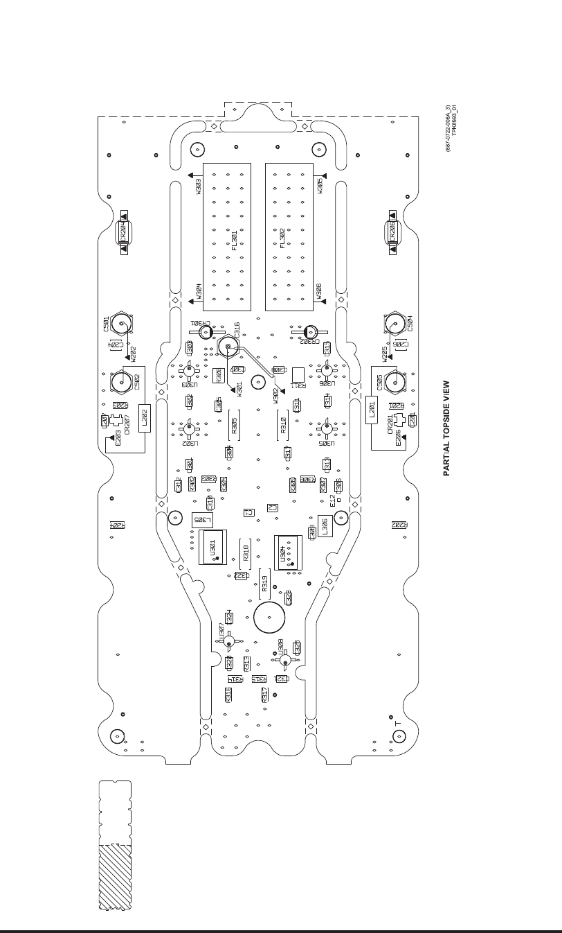
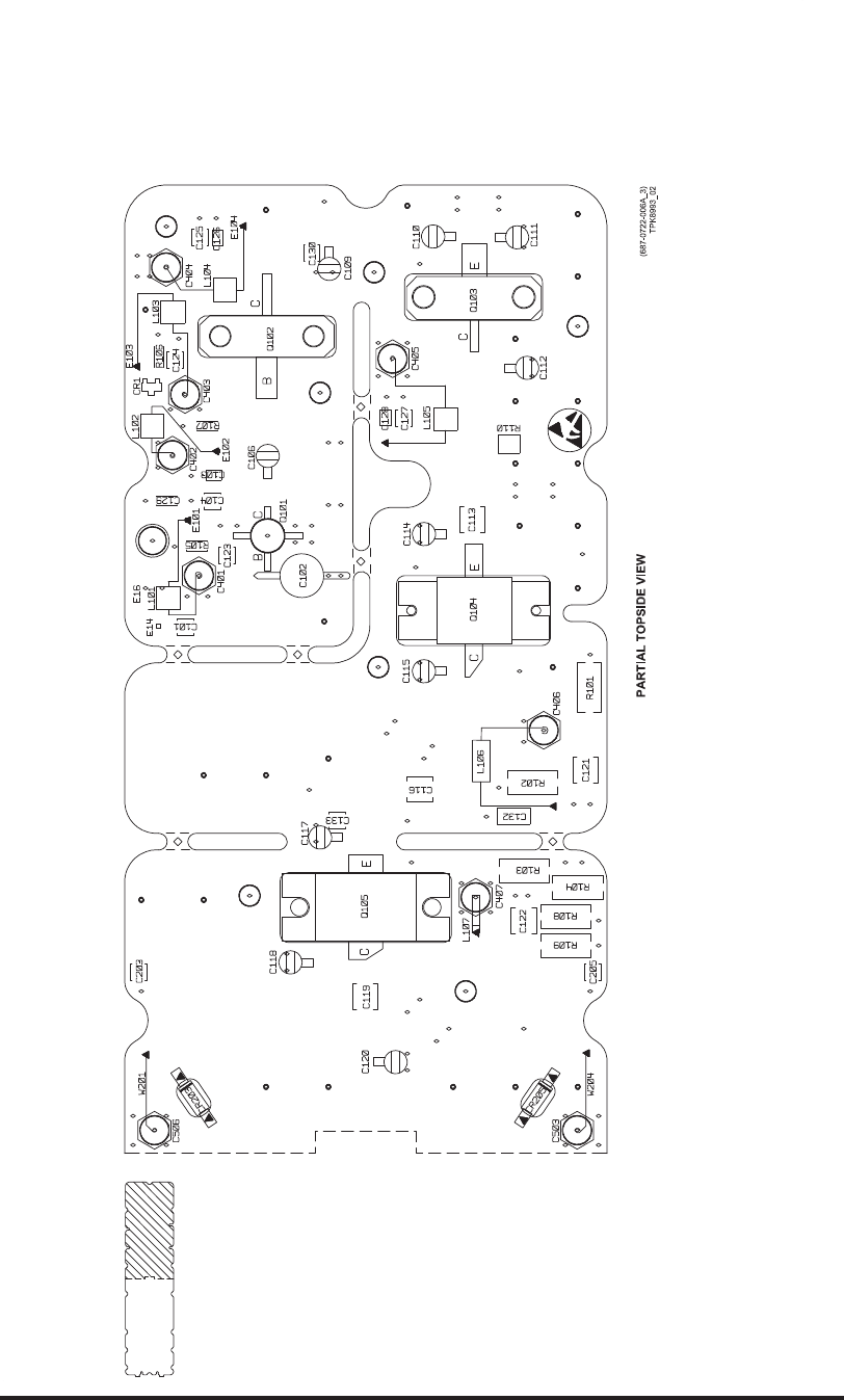
B. Maintenance Aid Diagrams
(1) The maintenance aid diagram shows the location of all components on the primary
assemblies. This diagram is before the schematic diagram in the manual. The
maintenance aid diagram also shows a history of the component configuration. The
maintenance aid diagram can look different than the circuit card/assembly.
SUBTASK 34-50-96-810-008-A01
C. Schematic Diagrams
(1) The schematic diagram helps the technician isolate a fault in a circuit to a defective
component. Where applicable, circuit voltages and test points are shown. The
schematic diagram shows the most correct electrical configuration at the time of print for
the manual. Refer to the schematic changes page shown before the maintenance aid
diagram for all changes made.
SUBTASK 34-50-96-810-009-A01
D. Configuration Effectivity
(1) Table 2002 shows the revision level (at the time of print) of circuit cards or subassemblies
of the TDR-94/94D that have a schematic diagram. Figure numbers for the maintenance
aid and schematic diagrams are also shown.
(2) Rockwell Collins uses the procedure that follows to identify the configuration (or revision
level) of a unit or subassembly.
(a) A 2-letter (maximum) identifier is shown after the letters REV (revision). If no
changes have been done, the identifier starts with - (dash). The first change is
34-50-96 Page 2005
May 18/06

ROCKWELL COLLINS
COMPONENT MAINTENANCE MANUAL with IPL
TDR-94, PART NO 622-9352
identified as A, the second as B, and continues through Y, then to AA, AB, and
continues to YY. (Letters I, O, Q, S, X, and Z are not used).
(b) Rework includes changes in a unit or a subassembly sent back to Rockwell Collins
for repair, or removed from the company's available units. At the time of rework, the
unit or subassembly is identified with the revision level mark (letter) of the changes
made. When done, the original mark is left on the unit or subassembly and the
letters RWK (rework) are added. This is followed with the letter identifier of the
newest revision done during rework. For example, unit one has the mark of REV B -
RWK F, and unit two has the mark of REV F. This shows that the two units are at
revision F, but unit one is reworked and can look different from the other.
NOTE: A reworked unit may not contain all the changes made to a new unit
with the same identifier. This unit does contain changes necessary to
make the unit operate the same as a new unit with the same identifier.
A unit reworked to a specified revision identifier can look different
from a new unit with the same revision identifier.
(c) This section includes only letter revision identifiers that cause schematic changes.
A unit or subassembly can have a letter identifier that comes between the identifiers
on the schematic changes page. Table 2002 can show a list that includes the
newest revision or other revisions. When this occurs, the schematic shows the
revision identifiers given on the Schematic Changes Page and can also show the
newest revision identifier.
SUBASSEMBLY/
UNITS
REVISION LEVEL COLLINS PART
NUMBER
MAINTENANCE
AID DIAGRAM
SCHEMATIC
DIAGRAM
High-Voltage Power
Supply Circuit Card
A1
L 687-0721-002 Figure 2001/
GRAPHIC 34-50-
96-99B-036-A01
Figure 2002/
GRAPHIC 34-50-
96-99B-037-A01
High-Voltage Power
Supply Circuit Card
A1
C 687-0721-003 Figure 2003/
GRAPHIC 34-50-
96-99B-038-A01
Figure 2004/
GRAPHIC 34-50-
96-99B-039-A01
Power Amplifier
Circuit Card A2
AA 687-0722-003 Figure 2005/
GRAPHIC 34-50-
96-99B-040-A01
Figure 2006/
GRAPHIC 34-50-
96-99B-041-A01
Power Amplifier
Circuit Card A2
K 687-0722-004 Figure 2007/
GRAPHIC 34-50-
96-99B-042-A01
Figure 2008/
GRAPHIC 34-50-
96-99B-043-A01
Assembly Revision Level and Diagram Reference Cont.
Table 2002/Table 34-50-96-99A-013-A01
34-50-96 Page 2006
May 18/06

ROCKWELL COLLINS
COMPONENT MAINTENANCE MANUAL with IPL
TDR-94, PART NO 622-9352
SUBASSEMBLY/
UNITS
REVISION LEVEL COLLINS PART
NUMBER
MAINTENANCE
AID DIAGRAM
SCHEMATIC
DIAGRAM
Power Amplifier
Circuit Card A2
A 687-0722-006 Figure 2008.1/
GRAPHIC 34-50-
96-99B-096-A01
Figure 2008.2/
GRAPHIC 34-50-
96-99B-097-A01
Modulator Circuit
Card A3
K 687-0723-004 Figure 2009/
GRAPHIC 34-50-
96-99B-044-A01
Figure 2010/
GRAPHIC 34-50-
96-99B-045-A01
Modulator Circuit
Card A3
B 687-0723-005 Figure 2011/
GRAPHIC 34-50-
96-99B-046-A01
Figure 2012/
GRAPHIC 34-50-
96-99B-047-A01
Synthesizer Circuit
Card A4
K 687-0724-002 Figure 2013/
GRAPHIC 34-50-
96-99B-048-A01
Figure 2014/
GRAPHIC 34-50-
96-99B-049-A01
Synthesizer Circuit
Card A4
D 687-0724-003 Figure 2015/
GRAPHIC 34-50-
96-99B-050-A01
Figure 2016/
GRAPHIC 34-50-
96-99B-051-A01
CPU-I/O
Programmed
Assembly A5
C 653-3674-001 Figure 2017/
GRAPHIC 34-50-
96-99B-052-A01
Figure 2019/
GRAPHIC 34-50-
96-99B-054-A01
CPU-I/O
Programmed
Assembly A5
B 653-3674-002 Figure 2017/
GRAPHIC 34-50-
96-99B-052-A01
Figure 2019/
GRAPHIC 34-50-
96-99B-054-A01
CPU-I/O
Programmed
Assembly A5
E 653-3674-003 Figure 2017/
GRAPHIC 34-50-
96-99B-052-A01
Figure 2019/
GRAPHIC 34-50-
96-99B-054-A01
CPU-I/O
Programmed
Assembly A5
D 653-3674-004 Figure 2017/
GRAPHIC 34-50-
96-99B-052-A01
Figure 2019/
GRAPHIC 34-50-
96-99B-054-A01
CPU-I/O
Programmed
Assembly A5
G 653-3674-005 Figure 2017/
GRAPHIC 34-50-
96-99B-052-A01
Figure 2019/
GRAPHIC 34-50-
96-99B-054-A01
CPU-I/O
Programmed
Assembly A5
F 653-3674-006 Figure 2017/
GRAPHIC 34-50-
96-99B-052-A01
Figure 2019/
GRAPHIC 34-50-
96-99B-054-A01
CPU-I/O
Programmed
Assembly A5
A 653-3674-007 Figure 2017/
GRAPHIC 34-50-
96-99B-052-A01
Figure 2019/
GRAPHIC 34-50-
96-99B-054-A01
Assembly Revision Level and Diagram Reference Cont.
Table 2002/Table 34-50-96-99A-013-A01
34-50-96 Page 2007
May 20/10

ROCKWELL COLLINS
COMPONENT MAINTENANCE MANUAL with IPL
TDR-94, PART NO 622-9352
SUBASSEMBLY/
UNITS
REVISION LEVEL COLLINS PART
NUMBER
MAINTENANCE
AID DIAGRAM
SCHEMATIC
DIAGRAM
CPU-I/O
Programmed
Assembly A5
A 653-3674-008 Figure 2017/
GRAPHIC 34-50-
96-99B-052-A01
Figure 2019/
GRAPHIC 34-50-
96-99B-054-A01
CPU-I/O
Programmed
Assembly A5
A 653-3674-009 Figure 2017/
GRAPHIC 34-50-
96-99B-052-A01
Figure 2019/
GRAPHIC 34-50-
96-99B-054-A01
CPU-I/O
Programmed
Assembly A5
A 653-3674-010 Figure 2017/
GRAPHIC 34-50-
96-99B-052-A01
Figure 2019/
GRAPHIC 34-50-
96-99B-054-A01
CPU-I/O
Programmed
Assembly A5
A 653-3674-011 Figure 2017/
GRAPHIC 34-50-
96-99B-052-A01
Figure 2019/
GRAPHIC 34-50-
96-99B-054-A01
CPU-I/O
Programmed
Assembly A5
A 653-3674-012 Figure 2017/
GRAPHIC 34-50-
96-99B-052-A01
Figure 2019/
GRAPHIC 34-50-
96-99B-054-A01
CPU-I/O
Programmed
Assembly A5
A 653-3674-013 Figure 2017/
GRAPHIC 34-50-
96-99B-052-A01
Figure 2019/
GRAPHIC 34-50-
96-99B-054-A01
CPU-I/O
Programmed
Assembly A5
A 653-3674-014 Figure 2017/
GRAPHIC 34-50-
96-99B-052-A01
Figure 2019/
GRAPHIC 34-50-
96-99B-054-A01
CPU-I/O
Programmed
Assembly A5
C 653-3674-015 Figure 2017/
GRAPHIC 34-50-
96-99B-052-A01
Figure 2019/
GRAPHIC 34-50-
96-99B-054-A01
CPU-I/O
Programmed
Assembly A5
C 653-3674-016 Figure 2017/
GRAPHIC 34-50-
96-99B-052-A01
Figure 2019/
GRAPHIC 34-50-
96-99B-054-A01
CPU-I/O
Programmed
Assembly A5
B 653-3674-017 Figure 2017/
GRAPHIC 34-50-
96-99B-052-A01
Figure 2019/
GRAPHIC 34-50-
96-99B-054-A01
CPU-I/O
Programmed
Assembly A5
B 653-3674-018 Figure 2017/
GRAPHIC 34-50-
96-99B-052-A01
Figure 2019/
GRAPHIC 34-50-
96-99B-054-A01
CPU-I/O Circuit
Card A5A1
(unprogrammed)
M 828-2700-002 Figure 2018/
GRAPHIC 34-50-
96-99B-053-A01
Figure 2019/
GRAPHIC 34-50-
96-99B-054-A01
Assembly Revision Level and Diagram Reference Cont.
Table 2002/Table 34-50-96-99A-013-A01
34-50-96 Page 2008
May 20/10

ROCKWELL COLLINS
COMPONENT MAINTENANCE MANUAL with IPL
TDR-94, PART NO 622-9352
SUBASSEMBLY/
UNITS
REVISION LEVEL COLLINS PART
NUMBER
MAINTENANCE
AID DIAGRAM
SCHEMATIC
DIAGRAM
CPU-I/O Circuit
Card A5A1
(unprogrammed)
C 828-2700-003 Figure 2020/
GRAPHIC 34-50-
96-99B-055-A01
Figure 2021/
GRAPHIC 34-50-
96-99B-056-A01
CPU-I/O
Programmed
Assembly A5
- 653-3674-025 Figure 2021.1/
GRAPHIC 34-50-
96-99B-098-A01
Figure 2021.2/
GRAPHIC 34-50-
96-99B-099-A01
CPU-I/O
Programmed
Assembly A5
- 653-3674-026 Figure 2021.1/
GRAPHIC 34-50-
96-99B-098-A01
Figure 2021.2/
GRAPHIC 34-50-
96-99B-099-A01
CPU-I/O Circuit
Card A5A1
(unprogrammed)
A 828-2700-004 Figure 2021.1/
GRAPHIC 34-50-
96-99B-098-A01
Figure 2021.2/
GRAPHIC 34-50-
96-99B-099-A01
Video Processor
Circuit Card A6
R 687-0726-004 Figure 2023/
GRAPHIC 34-50-
96-99B-058-A01
Figure 2024/
GRAPHIC 34-50-
96-99B-059-A01
Video Processor
Circuit Card A6
J 687-0726-005 Figure 2025/
GRAPHIC 34-50-
96-99B-060-A01
Figure 2026/
GRAPHIC 34-50-
96-99B-061-A01
Video Processor
Circuit Card A6
D 687-0726-006 Figure 2027/
GRAPHIC 34-50-
96-99B-062-A01
Figure 2028/
GRAPHIC 34-50-
96-99B-063-A01
Video Processor
Circuit Card A6
- 983-8019-001 Figure 2027/
GRAPHIC 34-50-
96-99B-062-A01
Figure 2028/
GRAPHIC 34-50-
96-99B-063-A01
Video Processor
Circuit Card A6
B 687-0726-007 Figure 2028.1/
GRAPHIC 34-50-
96-99B-100-A01
Figure 2028.2/
GRAPHIC 34-50-
96-99B-101-A01
IF Receiver, DPSK
Detector, and LVPS
Circuit Card A7
D 687-0727-004 Figure 2029/
GRAPHIC 34-50-
96-99B-064-A01
Figure 2030/
GRAPHIC 34-50-
96-99B-065-A01
IF Receiver, DPSK
Detector, and LVPS
Circuit Card A7
J 687-0727-005 Figure 2031/
GRAPHIC 34-50-
96-99B-066-A01
Figure 2032/
GRAPHIC 34-50-
96-99B-067-A01
Assembly Revision Level and Diagram Reference
Table 2002/Table 34-50-96-99A-013-A01
34-50-96 Page 2009/2010
May 20/10

ROCKWELL COLLINS
COMPONENT MAINTENANCE MANUAL with IPL
TDR-94, PART NO 622-9352
MAINTENANCE AID/SCHEMATIC CHANGES
REVISION
IDENT
(SHEET)
DESCRIPTION OF REVISION AND CAUSE FOR CHANGE SERVICE
BULLETIN
EFFECTIVITY
MARKING
N/A Printed wire board change only. REV A
N/A U20 changed from 351-1278-030 (type 2903) to 351-0656-010
(type 2901). Earlier part became obsolete.
REV B
N/A Data change only. REV C
D C29 changed from 184-2551-210 (10 wF) to 913-3670-740 (0.1
wF). Improve start-up time.
11 REV D
E For yield improvement: R32 changed from 705-3535-690, 432വ
to 705-3535-750, 499വR31 changed from 705-3537-330,
2.21kവto 705-3537-320, 2.15kവR33 changed from
705-3535-950, 825വto 705-3535-170, 845വR34 changed
from 705-3537-370, 2.43kവto 705-3537-380, 2.49kവ
REV E
N/A Replaced C1 thru C17 to eliminate use of gasket. New
capacitors have potted end to provide flat mounting surface.
REV F
N/A Deleted top washer from L2 mounting hardware. REV G
N/A Production process changes only. REV H and J
N/A Changed CPN of L2 mounting hardware. No change to
schematic.
REV K
N/A Internal documentation change only. REV L
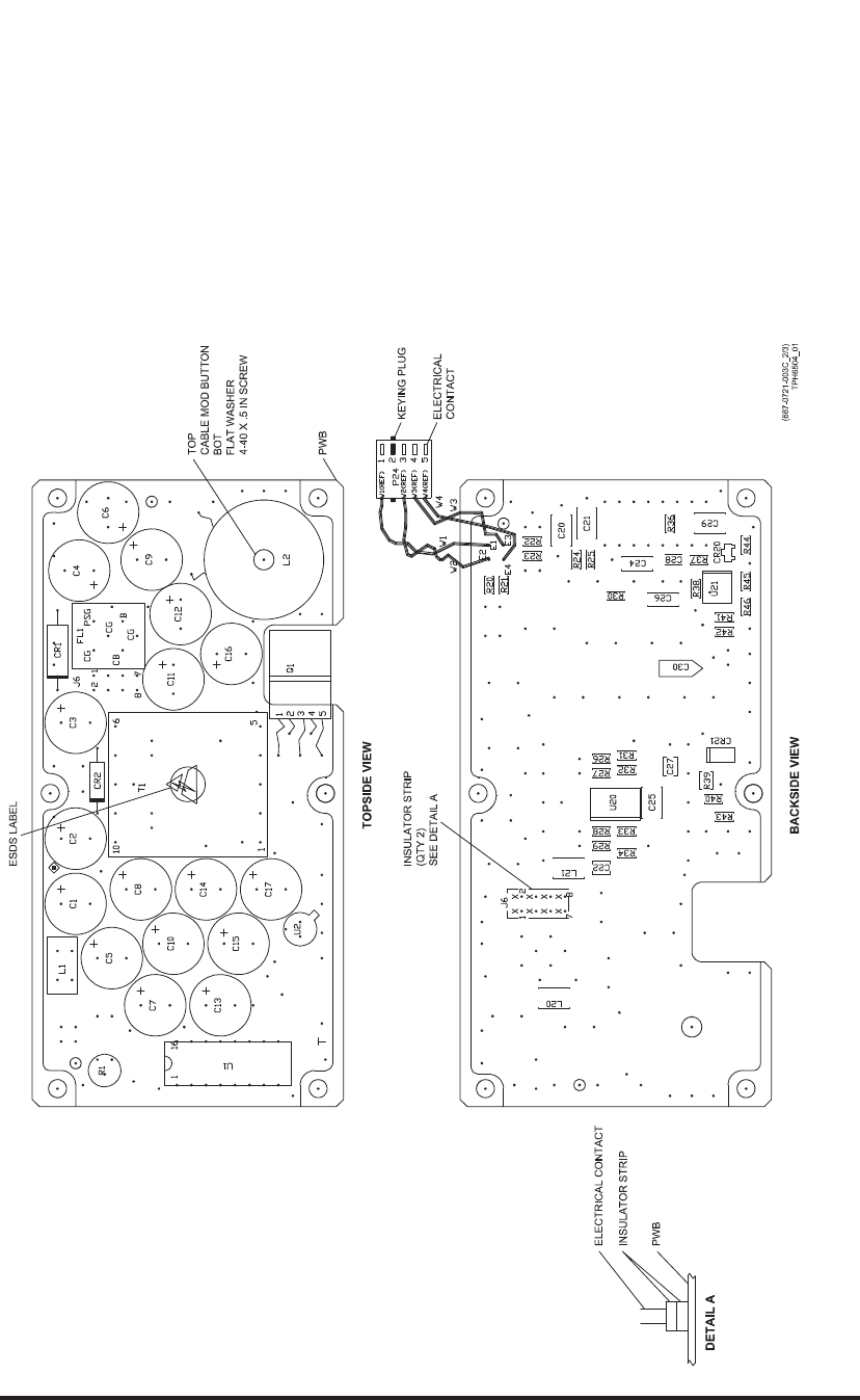
High Voltage Power Supply Circuit Card A1 (CPN 687-0721-002), Maintenance Aid and Schematic
Changes
Table 2003/Table 34-50-96-99A-014-A01
34-50-96 Page 2011/2012
May 18/06
ROCKWELL COLLINS
COMPONENT MAINTENANCE MANUAL with IPL
TDR-94, PART NO 622-9352
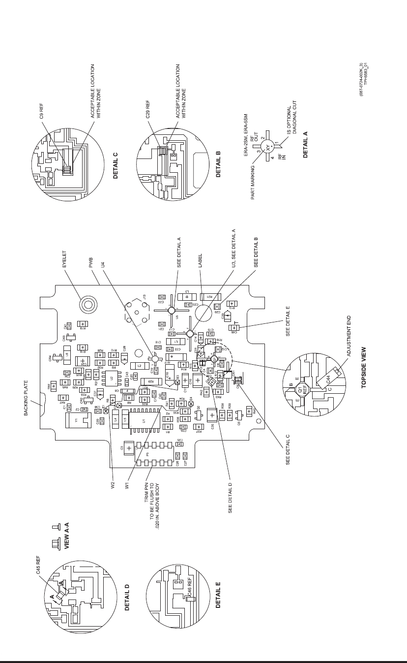
High Voltage Power Supply Circuit Card A1 (CPN 687-0721-002), Maintenance Aid Diagram
Figure 2001/GRAPHIC 34-50-96-99B-036-A01
34-50-96 Page 2013/2014
May 18/06
ROCKWELL COLLINS
COMPONENT MAINTENANCE MANUAL with IPL
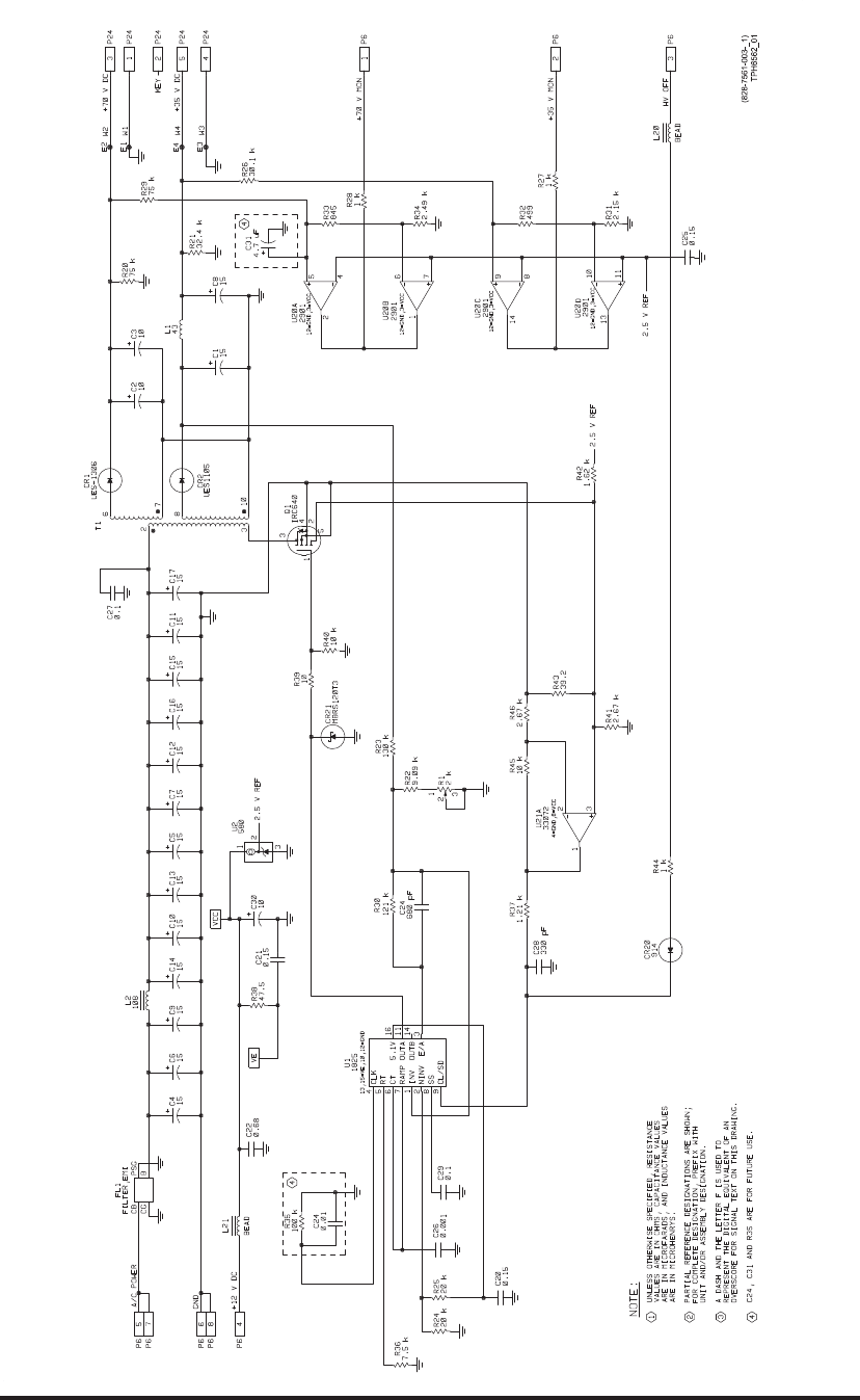
TDR-94, PART NO 622-9352
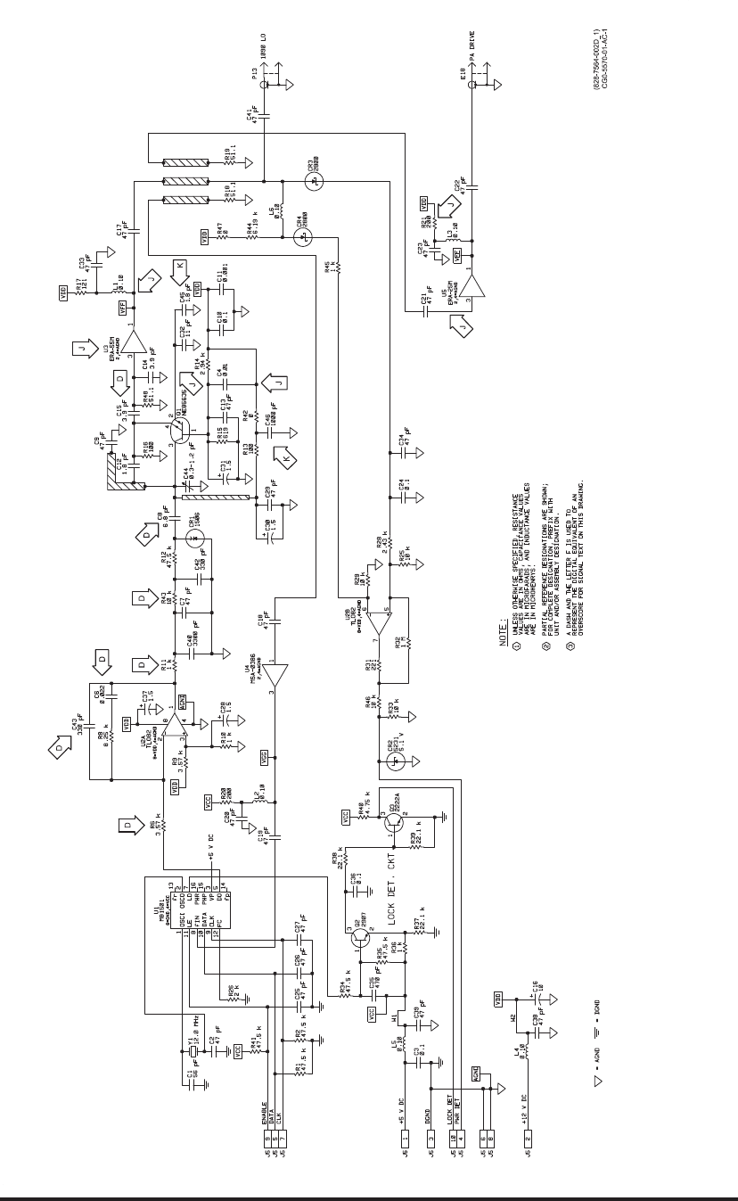
High Voltage Power SupplyCircuit Card A1 (CPN 687-0721-002), Schematic Diagram
Figure 2002/GRAPHIC 34-50-96-99B-037-A01
34-50-96 Page 2015/2016
May 18/06

ROCKWELL COLLINS
COMPONENT MAINTENANCE MANUAL with IPL
TDR-94, PART NO 622-9352
MAINTENANCE AID/SCHEMATIC CHANGES
REVISION
IDENT
(SHEET)
DESCRIPTION OF REVISION AND CAUSE FOR CHANGE SERVICE
BULLETIN
EFFECTIVITY
MARKING
N/A Implemented circuit card in TDR-94/94D main chassis
assemblies.
REV -
N/A Added silicone to circuit card to prevent capacitors from
moving.
REV A
N/A Internal documentation change only. REV B
N/A Changed CPN for L2 mounting screw. Previous CPN was
incorrect.
REV C
High Voltage Power Supply Circuit Card A1 (CPN 687-0721-003), Maintenance Aid and Schematic
Changes
Table 2004/Table 34-50-96-99A-015-A01
34-50-96 Page 2017/2018
May 18/06
ROCKWELL COLLINS
COMPONENT MAINTENANCE MANUAL with IPL
TDR-94, PART NO 622-9352
High Voltage Power Supply Circuit Card A1 (CPN 687-0721-003), Maintenance Aid Diagram
Figure 2003/GRAPHIC 34-50-96-99B-038-A01
34-50-96 Page 2019/2020
May 18/06
ROCKWELL COLLINS
COMPONENT MAINTENANCE MANUAL with IPL
TDR-94, PART NO 622-9352
High Voltage Power Supply Circuit Card A1 (CPN 687-0721-003), Schematic Diagram
Figure 2004/GRAPHIC 34-50-96-99B-039-A01
34-50-96 Page 2021/2022
May 18/06

ROCKWELL COLLINS
COMPONENT MAINTENANCE MANUAL with IPL
TDR-94, PART NO 622-9352
MAINTENANCE AID/SCHEMATIC CHANGES
REVISION
IDENT
(SHEET)
DESCRIPTION OF REVISION AND CAUSE FOR CHANGE SERVICE
BULLETIN
EFFECTIVITY
MARKING
N/A First production. REV B
N/A Relocated R302. REV C
D (2) Added L201 and L202; deleted W203 and W206 to correct
false power monitor indicator.
REV D
N/A Production assembly change only. REV E
F (2) Changed value of R302 and R303 to test selects so units with
lower than normal receiver gain can be adjusted.
REV F
N/A Data change only. REV G
N/A Changed conductive adhesive from 005-1021-010 to
005-0721-000.
REV H
J (1) Added R108 and R109 (20 ohms) and changed C132 from
0.056 to 0.01 wF to improve spectrum.
REV J
N/A Changed CR201 and CR207 part numbers; earlier parts are
not procurable.
REV K
N/A Added sleeving to U101 lead to prevent shorting to chassis. REV L
N/A Changed Q102, L305, and L306 part numbers; earlier parts
are not procurable.
REV M
N (2) Added C318, C319, and R312 to help the receiver pass the
side-lobe suppression test.
REV N
N/A Changed U301 and U304 part numbers; earlier parts are not
procurable.
REV P
N/A Data change only. REV R
T (1) Changed Q102 from type SD1802 to 23A008. REV T
U (2) Replaced diodes CR203 thru CR206 with a more robust part. REV U
N/A Production process change only. REV V
N/A Internal documentation change only. REV W and Y
AA (1) Changed Q102 from 23A008 to SD1802. Changed Q105 from
MRF10500 to MRF10502.
REV AA
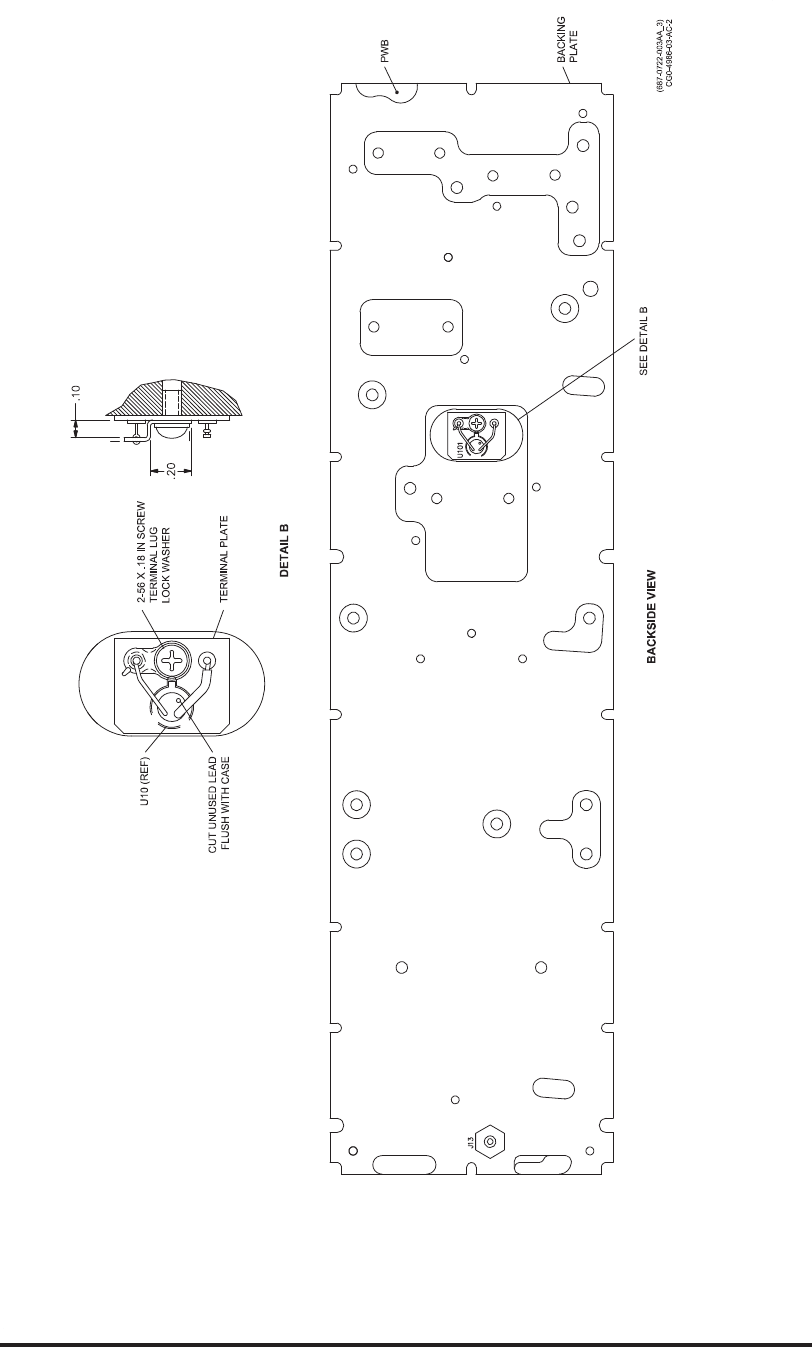
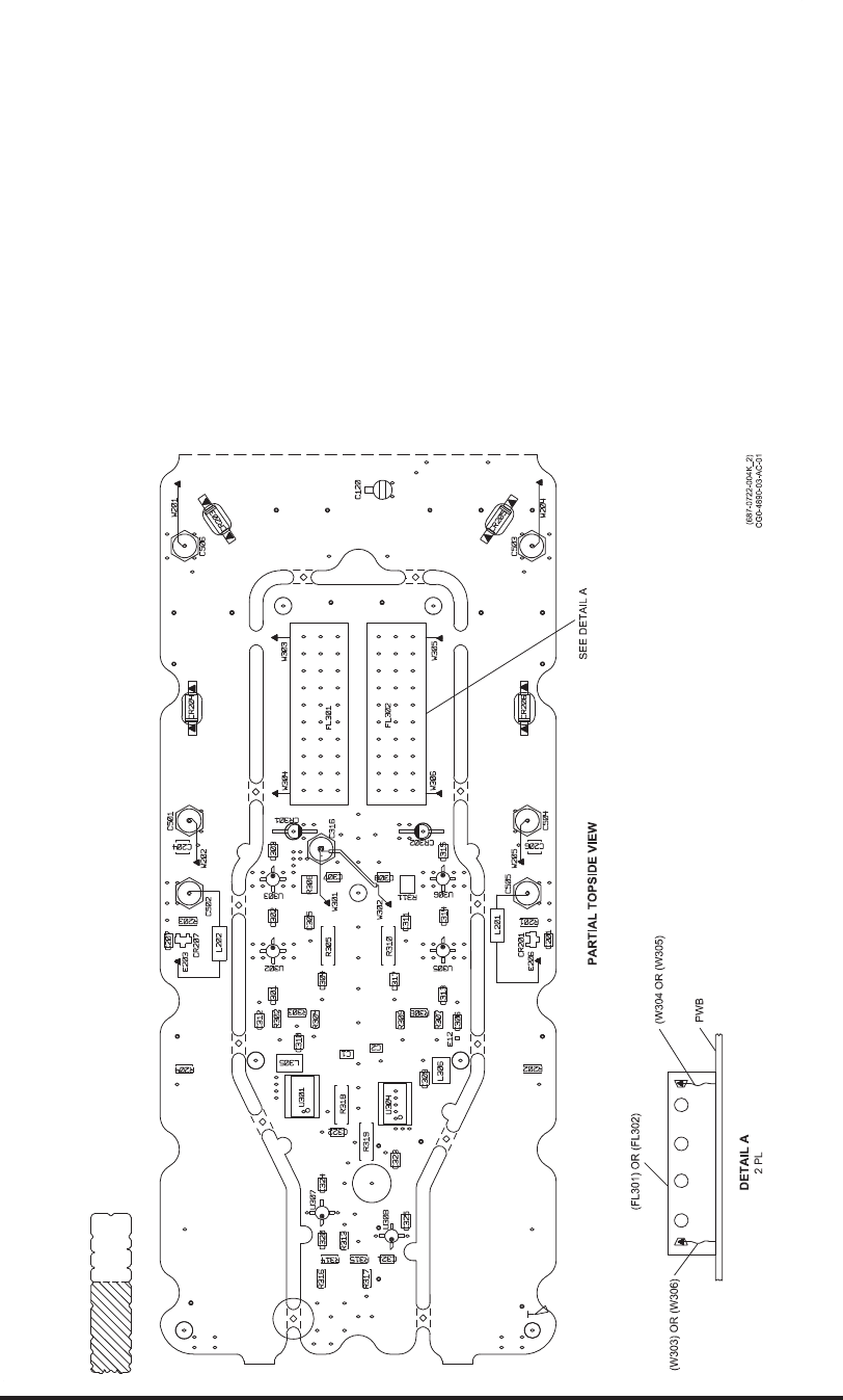
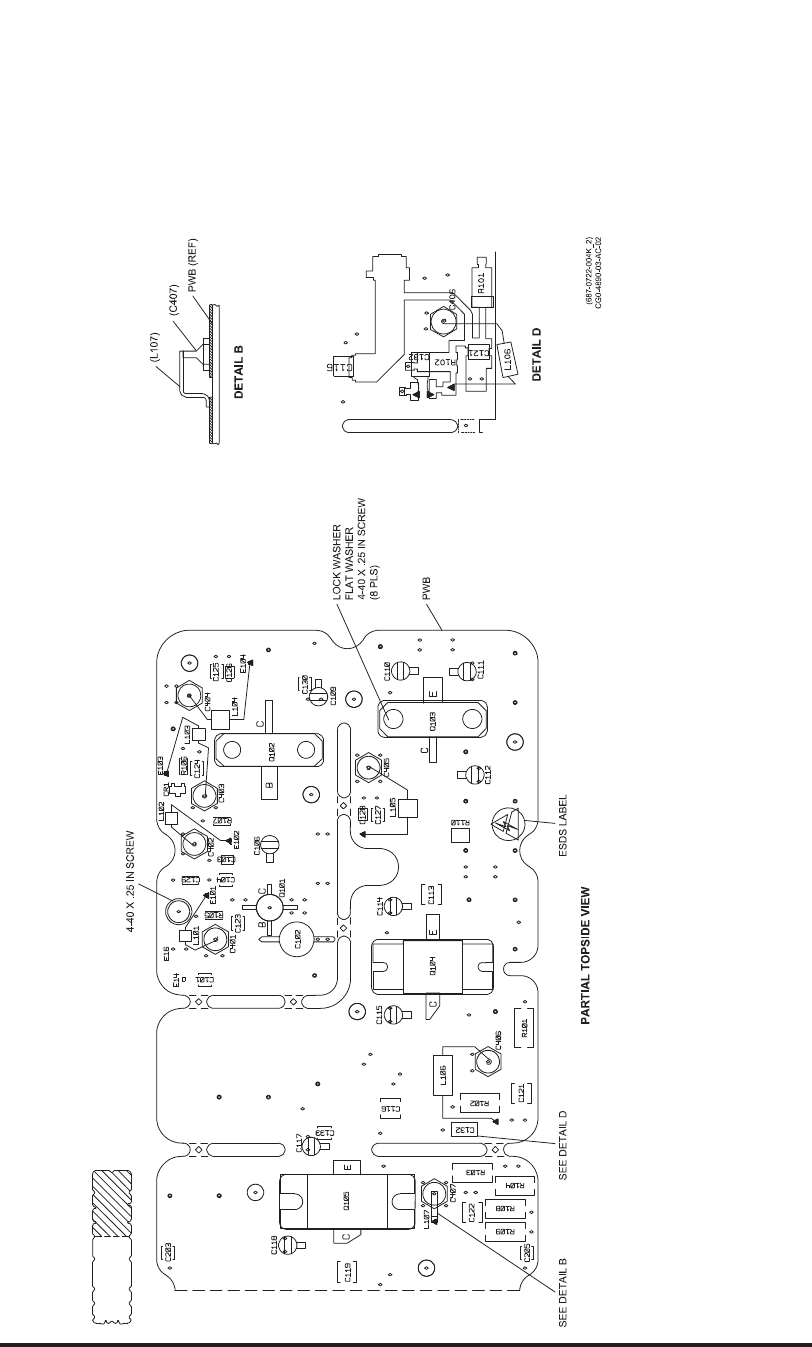
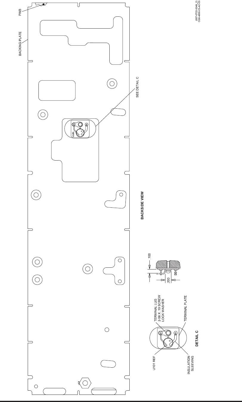
Power Amplifier Circuit Card A2 (CPN 687-0722-003), Maintenance Aid and Schematic Changes
Table 2005/Table 34-50-96-99A-016-A01
34-50-96 Page 2023/2024
May 18/06
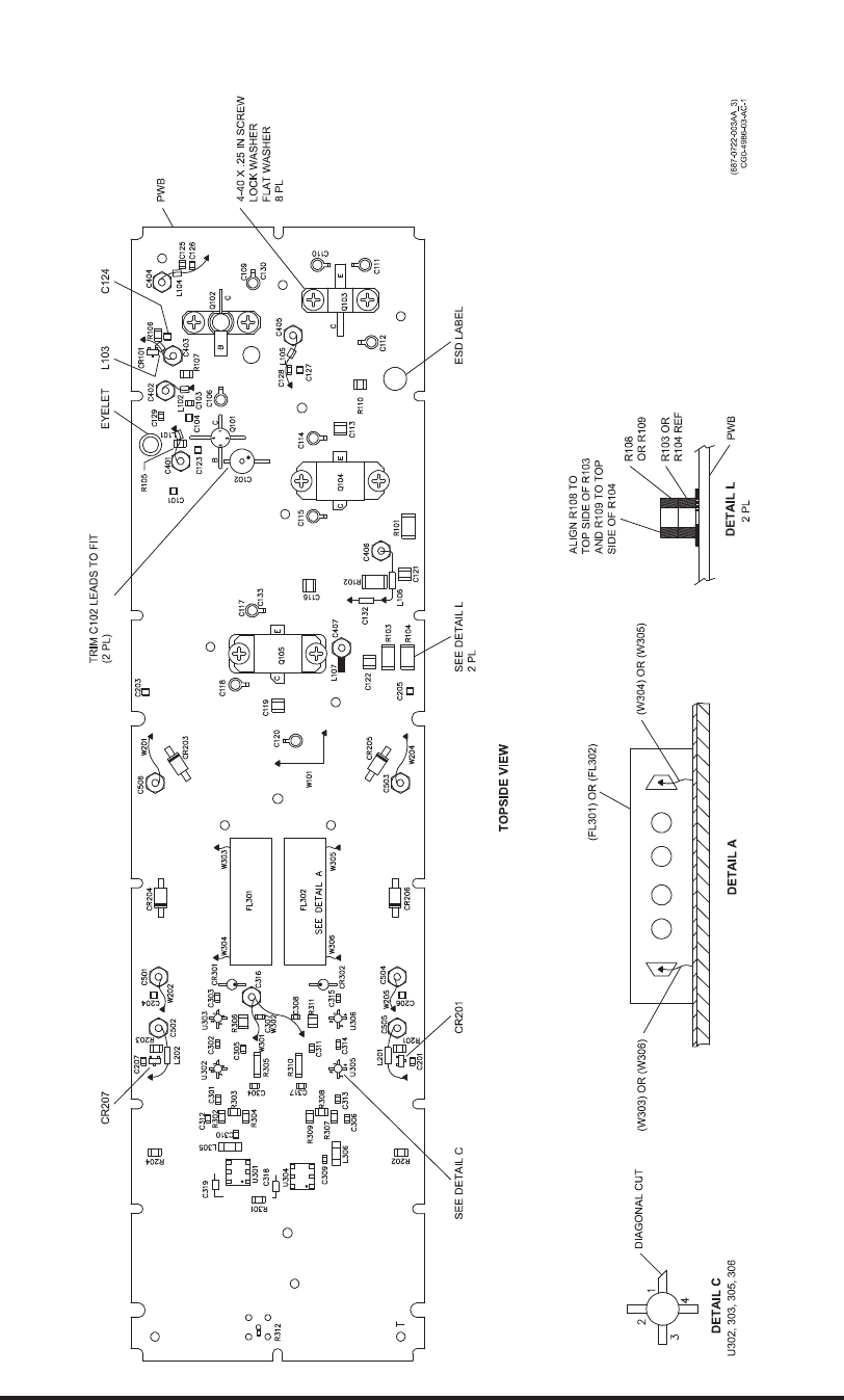
ROCKWELL COLLINS
COMPONENT MAINTENANCE MANUAL with IPL
TDR-94, PART NO 622-9352
Power Amplifier Circuit Card A2 (CPN 687-0722-003), Maintenance Aid Diagram
Figure 2005 (Sheet 1 of 3)/GRAPHIC 34-50-96-99B-040-A01
34-50-96 Page 2025/2026
May 18/06
ROCKWELL COLLINS
COMPONENT MAINTENANCE MANUAL with IPL
TDR-94, PART NO 622-9352
Power Amplifier Circuit Card A2 (CPN 687-0722-003), Maintenance Aid Diagram
Figure 2005 (Sheet 2 of 3)/GRAPHIC 34-50-96-99B-040-A01
34-50-96 Page 2027/2028
May 18/06
ROCKWELL COLLINS
COMPONENT MAINTENANCE MANUAL with IPL
TDR-94, PART NO 622-9352
Power Amplifier Circuit Card A2 (CPN 687-0722-003), Maintenance Aid Diagram
Figure 2005 (Sheet 3 of 3)/GRAPHIC 34-50-96-99B-040-A01
34-50-96 Page 2029/2030
May 18/06
ROCKWELL COLLINS
COMPONENT MAINTENANCE MANUAL with IPL
TDR-94, PART NO 622-9352
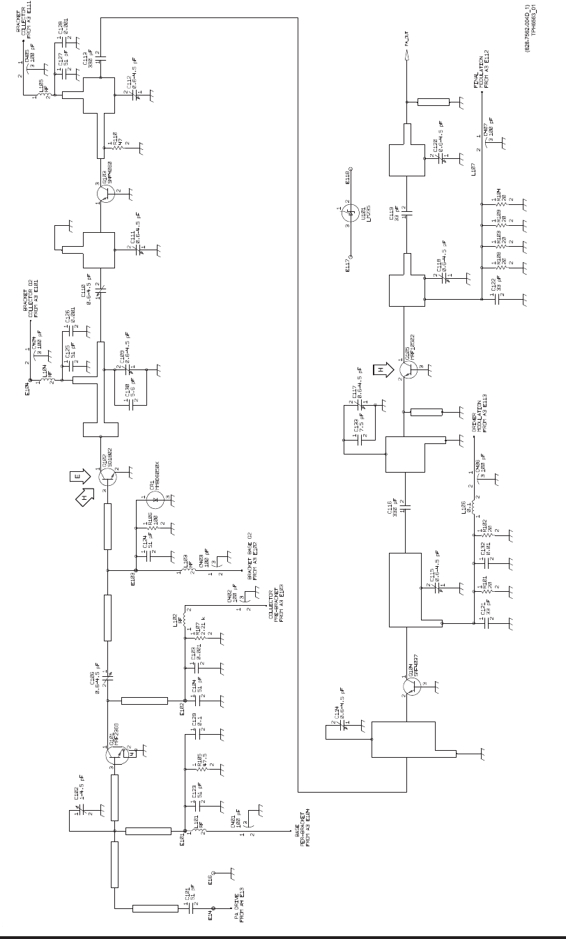
Power Amplifier Circuit Card A2 (CPN 687-0722-003), Schematic Diagram
Figure 2006 (Sheet 1 of 2)/GRAPHIC 34-50-96-99B-041-A01
34-50-96 Page 2031/2032
May 18/06
ROCKWELL COLLINS
COMPONENT MAINTENANCE MANUAL with IPL
TDR-94, PART NO 622-9352
Power Amplifier Circuit Card A2 (CPN 687-0722-003), Schematic Diagram
Figure 2006 (Sheet 2 of 2)/GRAPHIC 34-50-96-99B-041-A01
34-50-96 Page 2033/2034
May 18/06
ROCKWELL COLLINS
COMPONENT MAINTENANCE MANUAL with IPL
TDR-94, PART NO 622-9352
MAINTENANCE AID/SCHEMATIC CHANGES
REVISION
IDENT
(SHEET)
DESCRIPTION OF REVISION AND CAUSE FOR CHANGE SERVICE
BULLETIN
EFFECTIVITY
MARKING
N/A First production. REV A
N/A Replaced diodes CR203 thru CR206 with a more robust part. REV B
N/A Data error correction. REV C
N/A Removed item 3 heatsink compound; it is no longer required. REV D
E (1) Changed Q102 from SD1802 to 23A008 to improve production
yield. The SD1802 transistor is retained as a alternate part
that can be used if necessary.
REV E
F (2) Pin numbers of U301 and U304 were previously shown
incorrectly on schematic. These have been fixed.
REV F
N/A Internal documentation change only. REV G
H (1) Changed Q102 from 23A008 back to SD1802 and retained
the 23A008 transistor as the alternate part. Also changed
Q105 from MRF10500 to MRF10502.
REV H
N/A Added detail G to maintenance aid diagram to show the
correct installation of C132.
REV J
N/A Internal documentation change only. REV K
Power Amplifier Circuit Card A2 (CPN 687-0722-004), Maintenance Aid and Schematic Changes
Table 2006/Table 34-50-96-99A-017-A01
34-50-96 Page 2035/2036
May 18/06
ROCKWELL COLLINS
COMPONENT MAINTENANCE MANUAL with IPL
TDR-94, PART NO 622-9352
Power Amplifier Circuit Card A2 (CPN 687-0722-004), Maintenance Aid Diagram
Figure 2007 (Sheet 1 of 3)/GRAPHIC 34-50-96-99B-042-A01
34-50-96 Page 2037/2038
May 18/06
ROCKWELL COLLINS
COMPONENT MAINTENANCE MANUAL with IPL
TDR-94, PART NO 622-9352
Power Amplifier Circuit Card A2 (CPN 687-0722-004), Maintenance Aid Diagram
Figure 2007 (Sheet 2 of 3)/GRAPHIC 34-50-96-99B-042-A01
34-50-96 Page 2039/2040
May 18/06
ROCKWELL COLLINS
COMPONENT MAINTENANCE MANUAL with IPL
TDR-94, PART NO 622-9352
Power Amplifier Circuit Card A2 (CPN 687-0722-004), Maintenance Aid Diagram
Figure 2007 (Sheet 3 of 3)/GRAPHIC 34-50-96-99B-042-A01
34-50-96 Page 2041/2042
May 18/06
ROCKWELL COLLINS
COMPONENT MAINTENANCE MANUAL with IPL
TDR-94, PART NO 622-9352
Power Amplifier Circuit Card A2 (CPN 687-0722-004), Schematic Diagram
Figure 2008 (Sheet 1 of 3)/GRAPHIC 34-50-96-99B-043-A01
34-50-96 Page 2043/2044
May 18/06
ROCKWELL COLLINS
COMPONENT MAINTENANCE MANUAL with IPL
TDR-94, PART NO 622-9352
Power Amplifier Circuit Card A2 (CPN 687-0722-004), Schematic Diagram
Figure 2008 (Sheet 2 of 3)/GRAPHIC 34-50-96-99B-043-A01
34-50-96 Page 2045/2046
May 18/06
ROCKWELL COLLINS
COMPONENT MAINTENANCE MANUAL with IPL
TDR-94, PART NO 622-9352
Power Amplifier Circuit Card A2 (CPN 687-0722-004), Schematic Diagram
Figure 2008 (Sheet 3 of 3)/GRAPHIC 34-50-96-99B-043-A01
34-50-96 Page 2047/2048
May 18/06

ROCKWELL COLLINS
COMPONENT MAINTENANCE MANUAL with IPL
TDR-94, PART NO 622-9352
MAINTENANCE AID/SCHEMATIC CHANGES
REVISION
IDENT
(SHEET)
DESCRIPTION OF REVISION AND CAUSE FOR CHANGE SERVICE
BULLETIN
EFFECTIVITY
MARKING
(This sheet will contain maintenance aid and
schematic revision data.)
Power Amplifier Circuit Card A2 (CPN 687-0722-006), Maintenance Aid and Schematic Changes
Ta b l e 2006.1/Table 34-50-96-99A-043-A01
34-50-96 Page 2048.1/2048.2
May 20/10
ROCKWELL COLLINS
COMPONENT MAINTENANCE MANUAL with IPL
TDR-94, PART NO 622-9352
Power Amplifier Circuit Card A2 (CPN 687-0722-006), Maintenance Aid Diagram
Figure 2008.1 (Sheet 1 of 3)/GRAPHIC 34-50-96-99B-096-A01
34-50-96 Page 2048.3/2048.4
May 20/10
ROCKWELL COLLINS
COMPONENT MAINTENANCE MANUAL with IPL
TDR-94, PART NO 622-9352
Power Amplifier Circuit Card A2 (CPN 687-0722-006), Maintenance Aid Diagram
Figure 2008.1 (Sheet 2 of 3)/GRAPHIC 34-50-96-99B-096-A01
34-50-96 Page 2048.5/2048.6
May 20/10
ROCKWELL COLLINS
COMPONENT MAINTENANCE MANUAL with IPL
TDR-94, PART NO 622-9352
Power Amplifier Circuit Card A2 (CPN 687-0722-006), Maintenance Aid Diagram
Figure 2008.1 (Sheet 3 of 3)/GRAPHIC 34-50-96-99B-096-A01
34-50-96 Page 2048.7/2048.8
May 20/10
ROCKWELL COLLINS
COMPONENT MAINTENANCE MANUAL with IPL
TDR-94, PART NO 622-9352
Power Amplifier Circuit Card A2 (CPN 687-0722-006), Schematic Diagram
Figure 2008.2 (Sheet 1 of 3)/GRAPHIC 34-50-96-99B-097-A01
34-50-96 Page 2048.9/2048.10
May 20/10
ROCKWELL COLLINS
COMPONENT MAINTENANCE MANUAL with IPL
TDR-94, PART NO 622-9352
Power Amplifier Circuit Card A2 (CPN 687-0722-006), Schematic Diagram
Figure 2008.2 (Sheet 2 of 3)/GRAPHIC 34-50-96-99B-097-A01
34-50-96
Page 2048.11/
2048.12
May 20/10
ROCKWELL COLLINS
COMPONENT MAINTENANCE MANUAL with IPL
TDR-94, PART NO 622-9352
Power Amplifier Circuit Card A2 (CPN 687-0722-006), Schematic Diagram
Figure 2008.2 (Sheet 3 of 3)/GRAPHIC 34-50-96-99B-097-A01
34-50-96
Page 2048.13/
2048.14
May 20/10

ROCKWELL COLLINS
COMPONENT MAINTENANCE MANUAL with IPL
TDR-94, PART NO 622-9352
MAINTENANCE AID/SCHEMATIC CHANGES
REVISION
IDENT
(SHEET)
DESCRIPTION OF REVISION AND CAUSE FOR CHANGE SERVICE
BULLETIN
EFFECTIVITY
MARKING
A Q210, R245, R244 deleted and U103B added to prevent false
low-power diagnostics during self-test. These changes were
made before card was released to production.
REV A
B (1,2,3) Changed Q111, Q204 thru Q206, Q212, Q217, and Q218 from
IRFR9212 to IRFR9120; earlier part is not procurable. Also,
added R296 and R297 and changed values of R237 and R250.
REV B
C (2) Made C216 a test select because of variations in the pulse
width. Changed part numbers of R237 and R250 (ohm values
stayed the same but changed to 1/4W).
REV C
N/A Replaced Q211 part number; earlier part is not procurable. REV D
N/A For future part availability, changed R131 from carbon comp
to metal film.
REV E
N/A Data change only. REV F
G (1) Changed Q211 from MTD 8N06E to MTD 15N06V. The
transistor being replaced is obsolete.
REV G
H (2) Q106 is changed from IRF540 to IRF540N. The IRF540
transistor is no longer procurable.
REV H
N/A Internal documentation change only. REV J
K (2) Q106 is changed back to IRF540 because the IRF540N is now
obsolete.
REV K
Modulator Circuit Card A3 (CPN 687-0723-004), Maintenance Aid and Schematic Changes
Table 2007/Table 34-50-96-99A-018-A01
34-50-96 Page 2049/2050
May 18/06
ROCKWELL COLLINS
COMPONENT MAINTENANCE MANUAL with IPL
TDR-94, PART NO 622-9352
Modulator Circuit Card A3 (CPN 687-0723-004), Maintenance Aid Diagram
Figure 2009 (Sheet 1 of 2)/GRAPHIC 34-50-96-99B-044-A01
34-50-96 Page 2051/2052
May 18/06
ROCKWELL COLLINS
COMPONENT MAINTENANCE MANUAL with IPL
TDR-94, PART NO 622-9352
Modulator Circuit Card A3 (CPN 687-0723-004), Maintenance Aid Diagram
Figure 2009 (Sheet 2 of 2)/GRAPHIC 34-50-96-99B-044-A01
34-50-96 Page 2053/2054
May 18/06
ROCKWELL COLLINS
COMPONENT MAINTENANCE MANUAL with IPL
TDR-94, PART NO 622-9352
Modulator Circuit Card A3 (CPN 687-0723-004), Schematic Diagram
Figure 2010 (Sheet 1 of 4)/GRAPHIC 34-50-96-99B-045-A01
34-50-96 Page 2055/2056
May 18/06
ROCKWELL COLLINS
COMPONENT MAINTENANCE MANUAL with IPL
TDR-94, PART NO 622-9352
Modulator Circuit Card A3 (CPN 687-0723-004), Schematic Diagram
Figure 2010 (Sheet 2 of 4)/GRAPHIC 34-50-96-99B-045-A01
34-50-96 Page 2057/2058
May 18/06
ROCKWELL COLLINS
COMPONENT MAINTENANCE MANUAL with IPL
TDR-94, PART NO 622-9352
Modulator Circuit Card A3 (CPN 687-0723-004), Schematic Diagram
Figure 2010 (Sheet 3 of 4)/GRAPHIC 34-50-96-99B-045-A01
34-50-96 Page 2059/2060
May 18/06
ROCKWELL COLLINS
COMPONENT MAINTENANCE MANUAL with IPL
TDR-94, PART NO 622-9352
Modulator Circuit Card A3 (CPN 687-0723-004), Schematic Diagram
Figure 2010 (Sheet 4 of 4)/GRAPHIC 34-50-96-99B-045-A01
34-50-96 Page 2061/2062
May 18/06

ROCKWELL COLLINS
COMPONENT MAINTENANCE MANUAL with IPL
TDR-94, PART NO 622-9352
MAINTENANCE AID/SCHEMATIC CHANGES
REVISION
IDENT
(SHEET)
DESCRIPTION OF REVISION AND CAUSE FOR CHANGE SERVICE
BULLETIN
EFFECTIVITY
MARKING
NA Initial release. REV A
NA Documentation change only. REV B
C (2) Changed Q106 from IRF540N (non-procurable) to IRF540. REV C
Modulator Circuit Card A3 (CPN 687-0723-005), Maintenance Aid and Schematic Changes
Table 2008/Table 34-50-96-99A-019-A01
34-50-96 Page 2063/2064
May 18/06
ROCKWELL COLLINS
COMPONENT MAINTENANCE MANUAL with IPL
TDR-94, PART NO 622-9352
Modulator Circuit Card A3 (CPN 687-0723-005), Maintenance Aid Diagram
Figure 2011 (Sheet 1 of 2)/GRAPHIC 34-50-96-99B-046-A01
34-50-96 Page 2065/2066
May 18/06
ROCKWELL COLLINS
COMPONENT MAINTENANCE MANUAL with IPL
TDR-94, PART NO 622-9352
Modulator Circuit Card A3 (CPN 687-0723-005), Maintenance Aid Diagram
Figure 2011 (Sheet 2 of 2)/GRAPHIC 34-50-96-99B-046-A01
34-50-96 Page 2067/2068
May 18/06
ROCKWELL COLLINS
COMPONENT MAINTENANCE MANUAL with IPL
TDR-94, PART NO 622-9352
Modulator Circuit Card A3 (CPN 687-0723-005), Schematic Diagram
Figure 2012 (Sheet 1 of 4)/GRAPHIC 34-50-96-99B-047-A01
34-50-96 Page 2069/2070
May 18/06
ROCKWELL COLLINS
COMPONENT MAINTENANCE MANUAL with IPL
TDR-94, PART NO 622-9352
Modulator Circuit Card A3 (CPN 687-0723-005), Schematic Diagram
Figure 2012 (Sheet 2 of 4)/GRAPHIC 34-50-96-99B-047-A01
34-50-96 Page 2071/2072
May 18/06
ROCKWELL COLLINS
COMPONENT MAINTENANCE MANUAL with IPL
TDR-94, PART NO 622-9352
Modulator Circuit Card A3 (CPN 687-0723-005), Schematic Diagram
Figure 2012 (Sheet 3 of 4)/GRAPHIC 34-50-96-99B-047-A01
34-50-96 Page 2073/2074
May 18/06
ROCKWELL COLLINS
COMPONENT MAINTENANCE MANUAL with IPL
TDR-94, PART NO 622-9352
Modulator Circuit Card A3 (CPN 687-0723-005), Schematic Diagram
Figure 2012 (Sheet 4 of 4)/GRAPHIC 34-50-96-99B-047-A01
34-50-96 Page 2075/2076
May 18/06

ROCKWELL COLLINS
COMPONENT MAINTENANCE MANUAL with IPL
TDR-94, PART NO 622-9352
MAINTENANCE AID/SCHEMATIC CHANGES
REVISION
IDENT
(SHEET)
DESCRIPTION OF REVISION AND CAUSE FOR CHANGE SERVICE
BULLETIN
EFFECTIVITY
MARKING
N/A Data changes only. REV A and B
N/A Production process change only. REV C
D Changed following components to improve VCO stability:
R43from47.3to10kവ(705-3535-020)
R11from1.62to1kവ(705-3535-200)
R6 from 392 വto 3.57 kവ(705-3537-490)
C43 from 1000 to 330 pF (913-3667-200)
C15 from 2.7 to 3.9 pF (914-3500-060)
C8 from 2.7 to 6.8 pF (914-3500-100)
R8from7.5to8.25kവ(705-3537-780)
C6 from 0.018 to 0.022 wF (913-3670-470)
REV D
N/A Changed following components to standard parts: R18, R19,
R42, R47, and R48.
REV E
N/A Production process changes only. REV F and G
J (1) Changed U3 and U5 from CGY-40 to ERA-55M (U3) and
ERA-25M (U5). Changed R21 from 121വto 200വ. Changed
CPN of L1 and L3 (Inductance value does not change).
Changed CPN of C17, C21, C22, C41. Capacitor values do not
change. Capacitor C4 0.1wF and C14 3.9 pF were added.
REV J
K (1) Added capacitors C45 and C46 to eliminated spurs on
synthesizer circuit card.
REV K
Synthesizer Circuit Card A4 (CPN 687-0724-002), Maintenance Aid and Schematic Changes
Table 2009/Table 34-50-96-99A-020-A01
34-50-96 Page 2077/2078
May 18/06
ROCKWELL COLLINS
COMPONENT MAINTENANCE MANUAL with IPL
TDR-94, PART NO 622-9352
Synthesizer Circuit Card A4 (CPN 687-0724-002), Maintenance Aid Diagram
Figure 2013/GRAPHIC 34-50-96-99B-048-A01
34-50-96 Page 2079/2080
May 18/06
ROCKWELL COLLINS
COMPONENT MAINTENANCE MANUAL with IPL
TDR-94, PART NO 622-9352
Synthesizer Circuit Card A4 (CPN 687-0724-002), Schematic Diagram
Figure 2014/GRAPHIC 34-50-96-99B-049-A01
34-50-96 Page 2081/2082
May 18/06

ROCKWELL COLLINS
COMPONENT MAINTENANCE MANUAL with IPL
TDR-94, PART NO 622-9352
MAINTENANCE AID/SCHEMATIC CHANGES
REVISION
IDENT
(SHEET)
DESCRIPTION OF REVISION AND CAUSE FOR CHANGE SERVICE
BULLETIN
EFFECTIVITY
MARKING
N/A Implemented circuit card into production. REV A
N/A Internal documentation changes only. REV B and C
N/A Changed CPN of U413. The new U413 uses a different
AT90S2313. EEPROM device.
REV D
Synthesizer Circuit Card A4 (CPN 687-0724-003), Maintenance Aid and Schematic Changes
Table 2010/Table 34-50-96-99A-021-A01
34-50-96 Page 2083/2084
May 18/06
ROCKWELL COLLINS
COMPONENT MAINTENANCE MANUAL with IPL
TDR-94, PART NO 622-9352
Synthesizer Circuit Card A4 (CPN 687-0724-003), Maintenance Aid Diagram
Figure 2015/GRAPHIC 34-50-96-99B-050-A01
34-50-96 Page 2085/2086
May 18/06
ROCKWELL COLLINS
COMPONENT MAINTENANCE MANUAL with IPL
TDR-94, PART NO 622-9352
Synthesizer Circuit Card A4 (CPN 687-0724-003), Schematic Diagram
Figure 2016 (Sheet 1 of 2)/GRAPHIC 34-50-96-99B-051-A01
34-50-96 Page 2087/2088
May 18/06