Rohde and Schwarz TMU925 UHF DTV ATSC 1KW TO 2.5 KW TRANSMITTER FAMILY User Manual Part 2
Rohde & Schwarz Inc UHF DTV ATSC 1KW TO 2.5 KW TRANSMITTER FAMILY Part 2
UserManual.wiki
>
Rohde and Schwarz
>
TMU925 User Manual
>
User Manual Part 2
Contents
1.
User Manual Part 1
2.
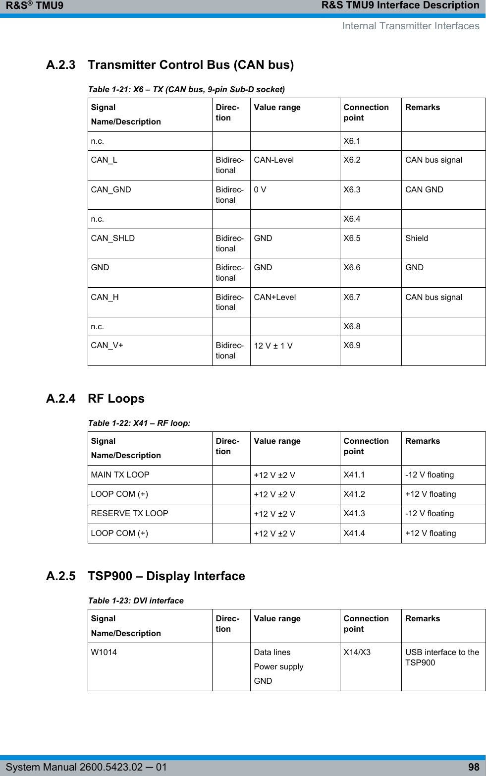
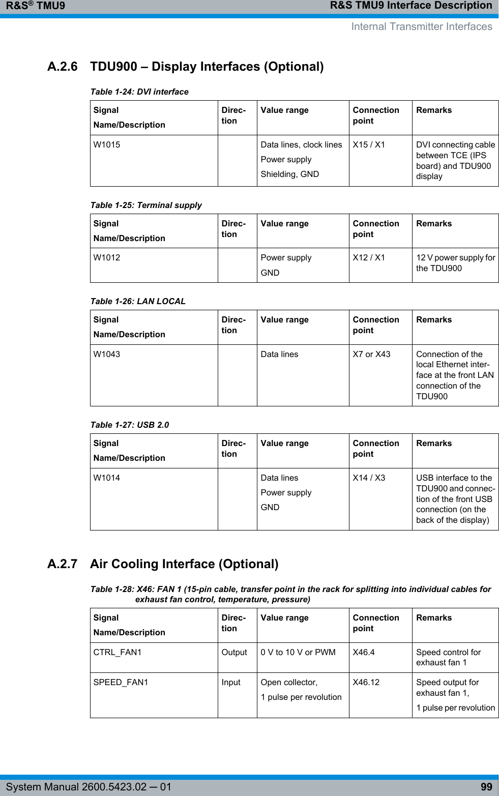
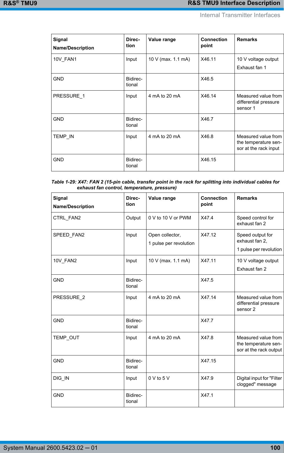
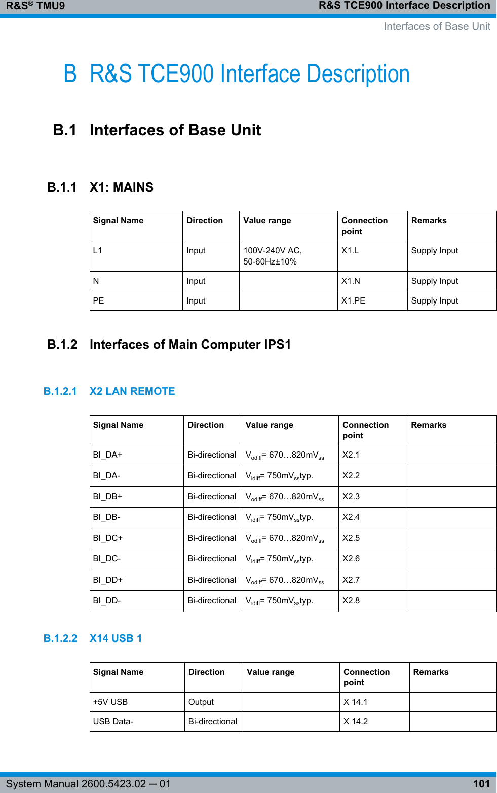
User Manual Part 2
User Manual Part 2
Navigation menu
Upload a User Manual
Namespaces
Wiki Guide
HTML
PDF
Info
Views
User Manual
Discussion / Help
Navigation