Rohde and Schwarz TMU925 UHF DTV ATSC 1KW TO 2.5 KW TRANSMITTER FAMILY User Manual Part 2
Rohde & Schwarz Inc UHF DTV ATSC 1KW TO 2.5 KW TRANSMITTER FAMILY Part 2
Contents
- 1. User Manual Part 1
- 2. User Manual Part 2
User Manual Part 2
Transmitter System R&S TMU9
R&S® TMU9
58System Manual 2600.5423.02 ─ 01
trays. When routing in solid cable ducts, use the next largest cable cross-sections and
fuse ratings.
The fuse ratings apply for a maximum ambient temperature of 25 °C and a minimum
undervoltage of 197 V AC.
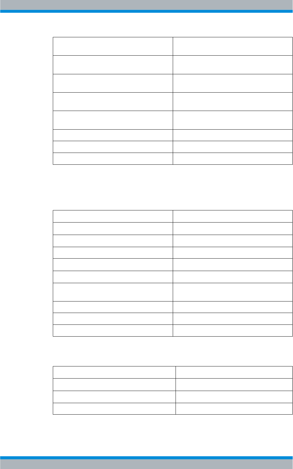
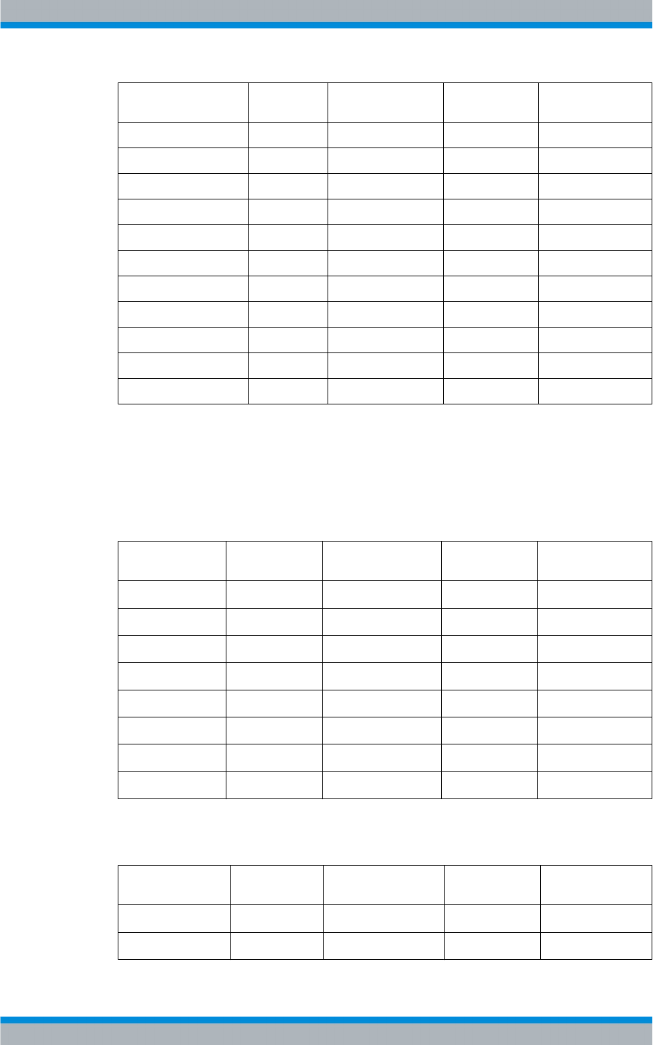
Series fuses and cable cross-sections for a 3-phase power supply
For a 230/400 V AC, 50 Hz power supply with L1, L2, L3, N, and PE, the following infor-
mation applies:
Number of amplifiers Series fuse pH gG Cable cross-section
1 3 x 40 A 5 x 6 mm2
2 3 x 40 A 5 x 6 mm2
3 3 x 40 A 5 x 6 mm2
4 3 x 40 A 5 x 6 mm2
5 3 x 40 A 5 x 6 mm2
6 3 x 40 A 5 x 6 mm2
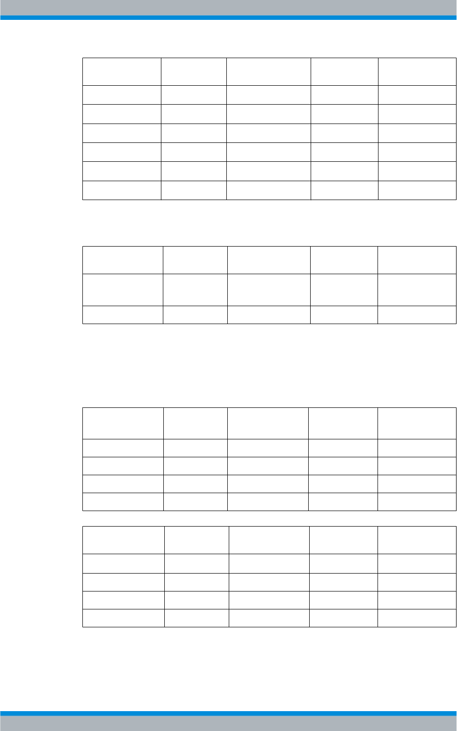
Series fuses and cable cross-sections for a 1-phase power supply
For a 230 V AC, 50 Hz power supply with L1, N, and PE, the following information applies:
Number of amplifiers Series fuse NH gG Cable cross-section
1 3 x 40 A 3 x 6 mm2
2 3 x 40 A 3 x 6 mm2
3 3 x 50 A 3 x 10 mm2
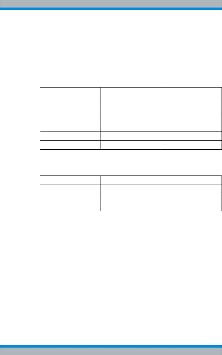
1. Run a power input cable of sufficient length to the series fuse.
2. Connect the cable to the series fuse.
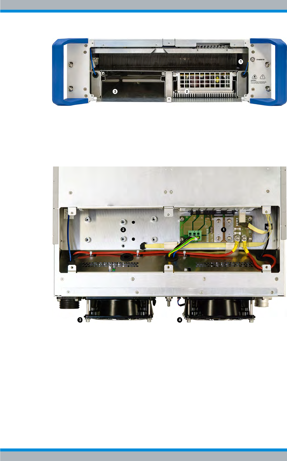
3. Loosen the clamping screws at the strain relief (item 1 in the following figure).
4. Run a cable from the series fuse through the strain relief to the power input terminal
X1 (item 3).
5. Remove the protective covers (item 2), open the respective terminals using a size 3
flat-head screwdriver, and connect the wires using the cable and terminal designa-
tions.
6. Check that the wires are secure and put the protective covers (item 2) back on.
7. Tighten the clamping screws of the strain relief.
8. Fasten the transparent protective cover to the rear of the mains distribution unit.
Installation R&S TMU9
Transmitter System R&S TMU9
R&S® TMU9
59System Manual 2600.5423.02 ─ 01
Fig. 3-13: Connecting the Power Input Cable
1 = Strain relief
2 = Protective covers
3 = Power input terminal X1
3.2.7 Installing the RF output
The output to the main antenna is an EIA connector. It is on the left-hand side of the
transmitter roof, next to the directional coupler and connection panel.
3.2.7.1 Connecting the Antenna
Connect the antenna as follows, depending on the transmitter type:
►Fasten the coaxial cable, which is preassembled to the station, to the EIA flange of
the transmitter's RF output. To prevent the screw connection from loosening, secure
it using a plain washer and spring lock washer.
● Use 4 screws M8, 35 mm (for EIA 1 5/8")
In regions with high humidity, the supplied rubber ring can be inserted into the groove
between the two EIA flanges.
3.2.7.2 Connecting the Dummy Antenna
The dummy antenna is connected only when putting the system into operation or for
maintenance and repair purposes.
Installation R&S TMU9
Transmitter System R&S TMU9
R&S® TMU9
60System Manual 2600.5423.02 ─ 01
With some dummy antennas that have coolant monitoring and overtemperature moni-
toring, the monitoring equipment can be connected to the transmitter. The main RF carrier
loop X41.1 and X41.2 on the CAN bus adapter or exciter switch can be used here as a
temporary measure (e.g. while the unit is being put into operation).
1. To connect the main RF carrier loop, use the inserted jumper plug and remove the
jumper.
2. Connect the monitoring cable in place of the jumper.
If you are using an RF patch panel that allows you to switch between the antenna and
dummy antenna by means of an RF bridging link (permanent installation), attach the
dummy antenna monitoring unit to the standby RF carrier loop (X41.1 and X41.2 with
CAN bus adapter, X41.3 and X41.4 with exciter switch). For more details, see chap-
ter 3.2.9, "Installing the RF Loop", on page 62.
3.2.8 Installing R&S TCE900 Customer Interfaces
The various versions of the TCE900 are already integrated into the rack with the delivery
of a transmitter. Installation is limited to wiring at the device's customer interfaces. Which
cables need to be connected depends on the transmitter configuration, the device version
and the custom requirements.
The cables used to provide ASI, 10MHz, PPS and GPS signals, should be double shiel-
ded.
IP and Ethernet connections should use class CAT6 cables should be used.
Please refer to the system circuit diagram for the system wiring applicable to your system.
The following steps are required to install a R&S TCE900.
1. Insert the R&S TCE900 into the TCE pull‑out frame without canting it (only one run-
ner) and carefully push the unit back to the front stop.
2. Fasten the R&S TCE900 to the TCE pull‑out frame using the two knurled screws.
3. Connect the cable in accordance with the wiring diagram and target designation.
4. Complete the TCE pull‑out frame with the front panel
a) To connect the Tx Control or Exciter A (for single drive) and TSP, plug the control
cable into the mini USB socket on the TSP900.
b) Hook the eyelets on the rear of the front panel into the hooks on the TCE pull-out
frame and press the front panel down as far as it will go.
c) Retighten the front panel to the sides of the TCE pull-out frame using four screws
(size 20 Torx screwdriver).
5. Slide the TCE pull-out frame into the rack.
Installation R&S TMU9
Transmitter System R&S TMU9
R&S® TMU9
61System Manual 2600.5423.02 ─ 01
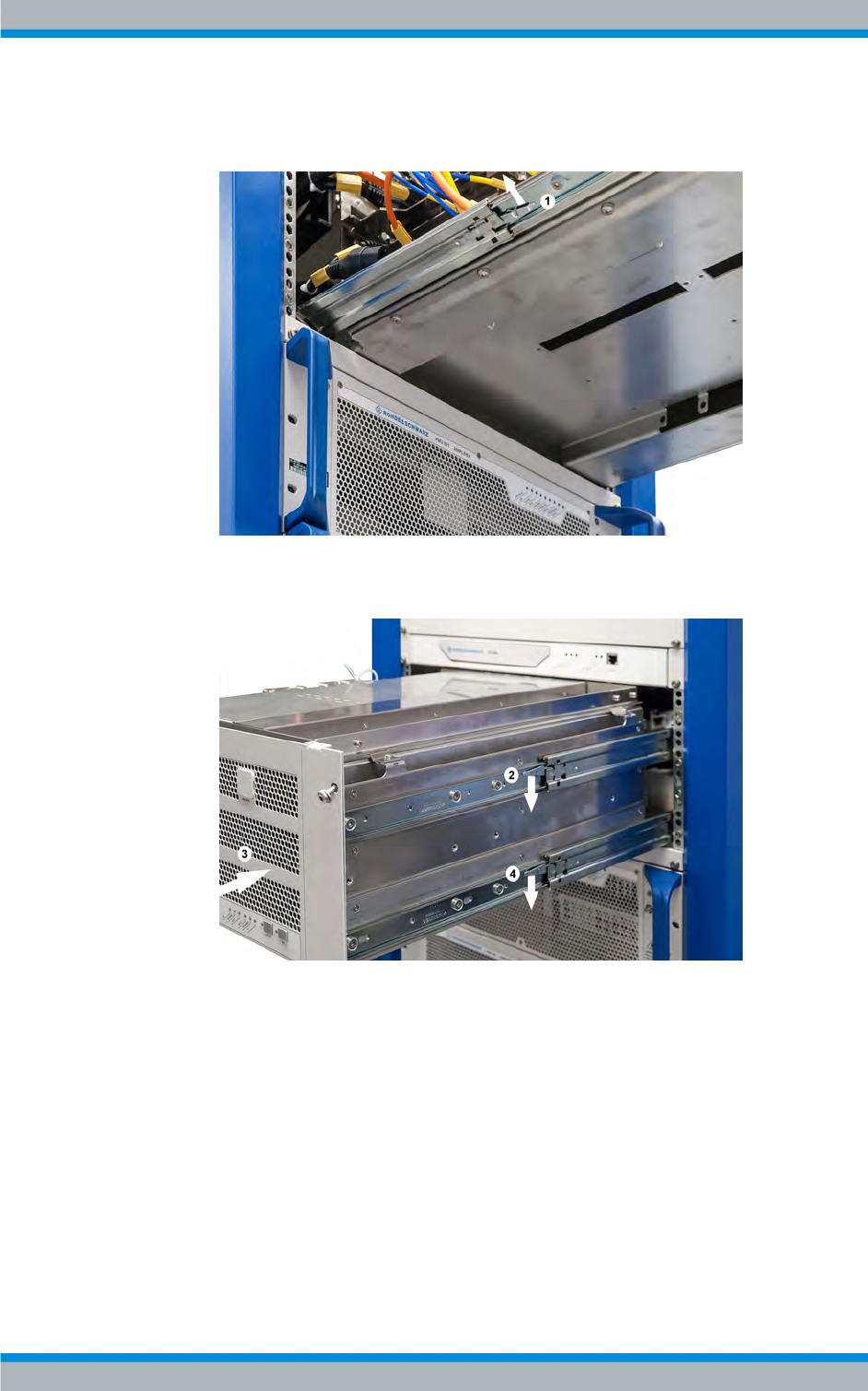
a) Push the left safety lever outwards and press one of the two right safety levers
downwards.
Fig. 3-14: Releasing the safety lever (left side).
1 = Push the safety lever outward and hold it
Fig. 3-15: Releasing the safety lever (right side).
2 = Press down and hold the first safety lever
3 = Push the TCE pull-out unit toward the rack
4 = Push the second safety lever downwards, hold it, and push the TCE pull-out unit in all the way
b) First hold the two safety levers in this position and press the TCE pull-out frame
toward the rack, until the safety lever retains its position on its own.
c) Also push the second safety lever on the right side downwards now and slide the
TCE pull-out unit into the rack.
d) Retighten the four captive screws on the TCE pull-out frame.
Installation R&S TMU9
Transmitter System R&S TMU9
R&S® TMU9
62System Manual 2600.5423.02 ─ 01
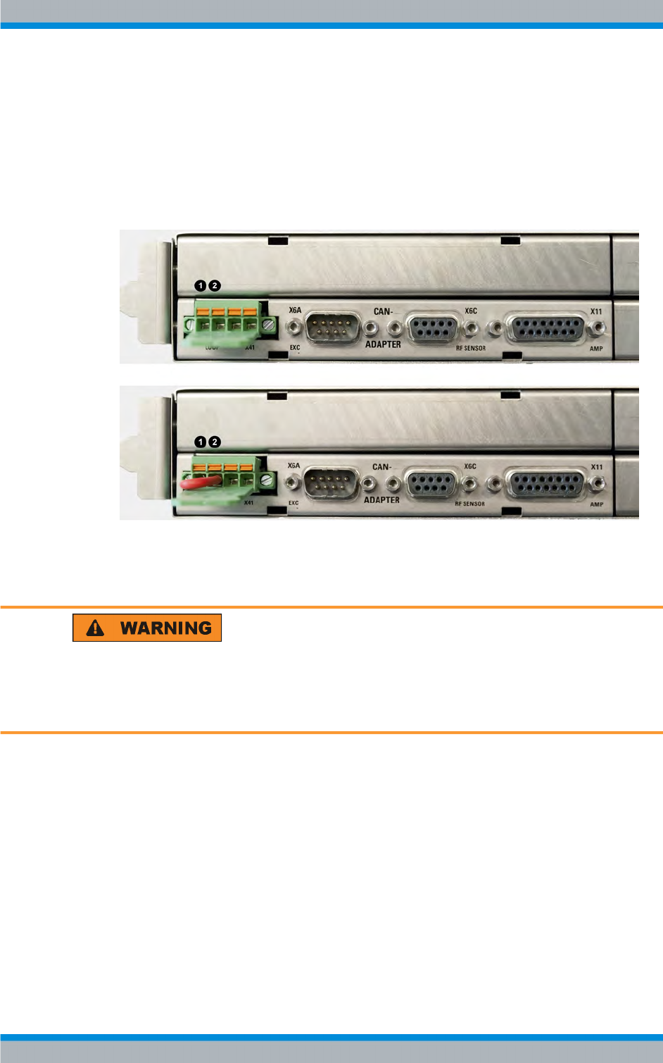
3.2.9 Installing the RF Loop
3.2.9.1 Single Drive (CAN Bus Adapter)
A RF loop plug is plugged onto the CAN bus adapter (in the system component frame)
that may have to be wired depending on whether or not the RF loop is used.
Fig. 3-16: RF loop plug X41 (LOOP), open and bypassed
1 = Pin 1
2 = Pin 2
Risk of RF Burns
Interruptions to the RF sector during operation can lead to arc flashes and severe burns
including shock that result from them. Before putting the transmitter into operation, ensure
that the available RF interlock systems are connected correctly.
The RF loop is not used
► Bridge pins 1 and 2 on RF loop plug X41 (LOOP) using a jumper.
The RF loop is used
► Loop pins 1 and 2 from plug X41 (LOOP) into the RF loop connections coming from
the RF sector (RF switch, switchover panel, etc.).
Installation R&S TMU9
Transmitter System R&S TMU9
R&S® TMU9
63System Manual 2600.5423.02 ─ 01
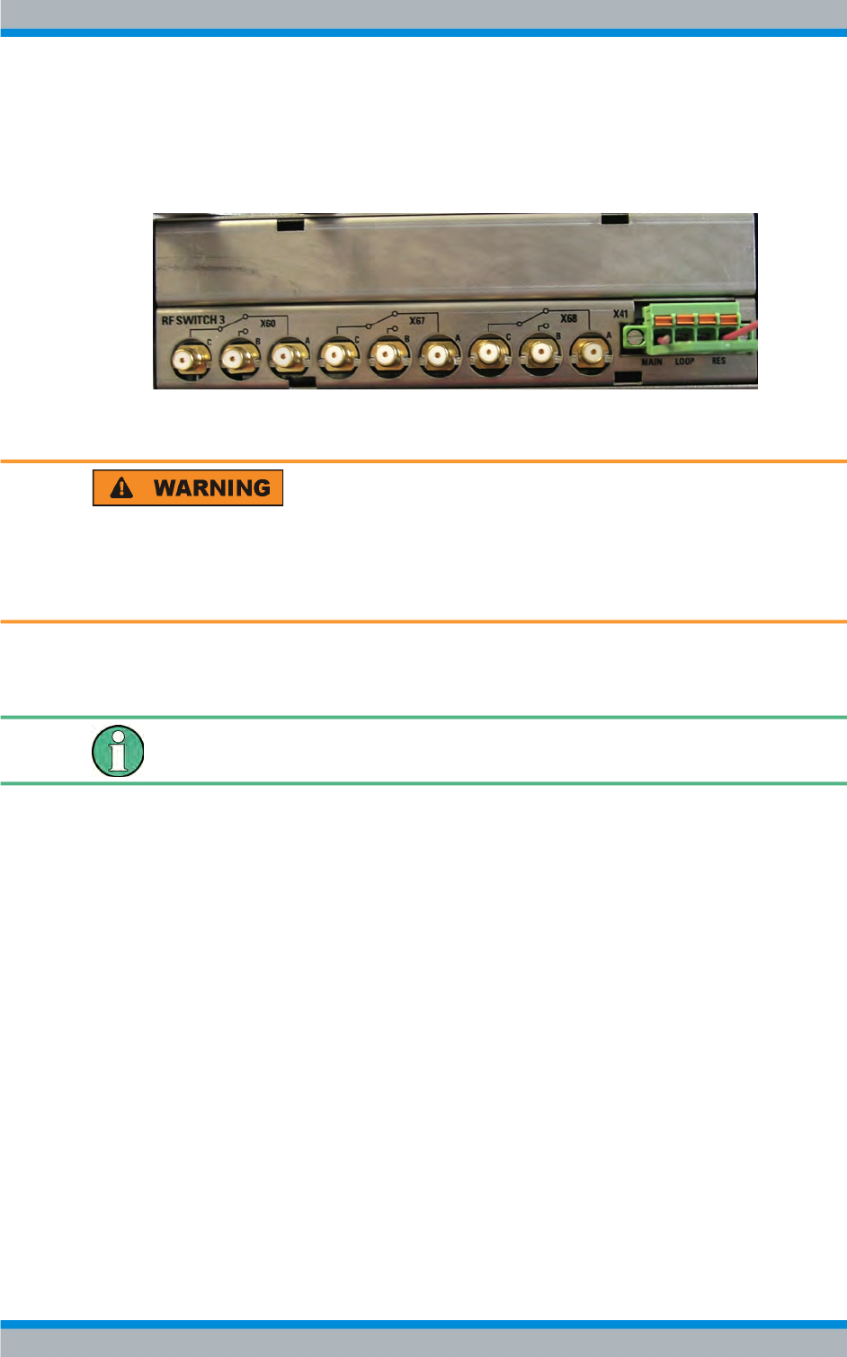
3.2.9.2 Dual Drive (RF Switch)
A RF loop plug is plugged onto the RF switch (in the system component frame) that may
have to be wired depending on whether or not the RF loop is used.
Fig. 3-17: RF loop plug X41 (LOOP) - RF Switch
Risk of RF Burns
Interruptions to the RF sector during operation can lead to arc flashes and severe burns
including shock that result from them. Before putting the transmitter into operation, ensure
that the available RF interlock systems are connected correctly.
In case of Dual Drive, the RF loop of the standby exciter is always bypassed via the exciter
switch.
This is not valid for Dual Drive with active dual output stage.
The external RF loop is only used for the active exciter.
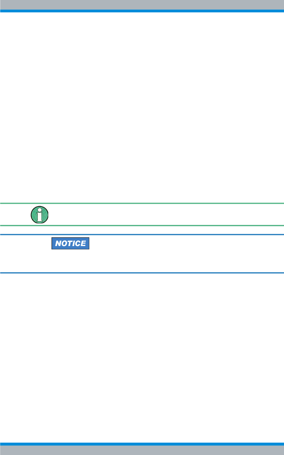
3.2.10 Installing the TM9-C1 Exhaust Kit
The following modules and components of the cooling system or exhaust kit are preas-
sembled at the factory:
●Air Cooling Interface ACIF as rackmount in the R&S TCE900-SystemControl unit
●Exhaust air transfer duct (item 1 in the following figure) on the rear part of the trans-
mitter roof
●Fans E1 and E2 in the rear door of the transmitter rack
●Pressure sensors S1 and S2 in the rear door of the transmitter rack
●Temperature sensors B1 and B2 in the rear door of the transmitter rack
The rear door with the preassembled components is delivered in separate packaging.
The following steps are required:
Installation R&S TMU9
Transmitter System R&S TMU9
R&S® TMU9
64System Manual 2600.5423.02 ─ 01
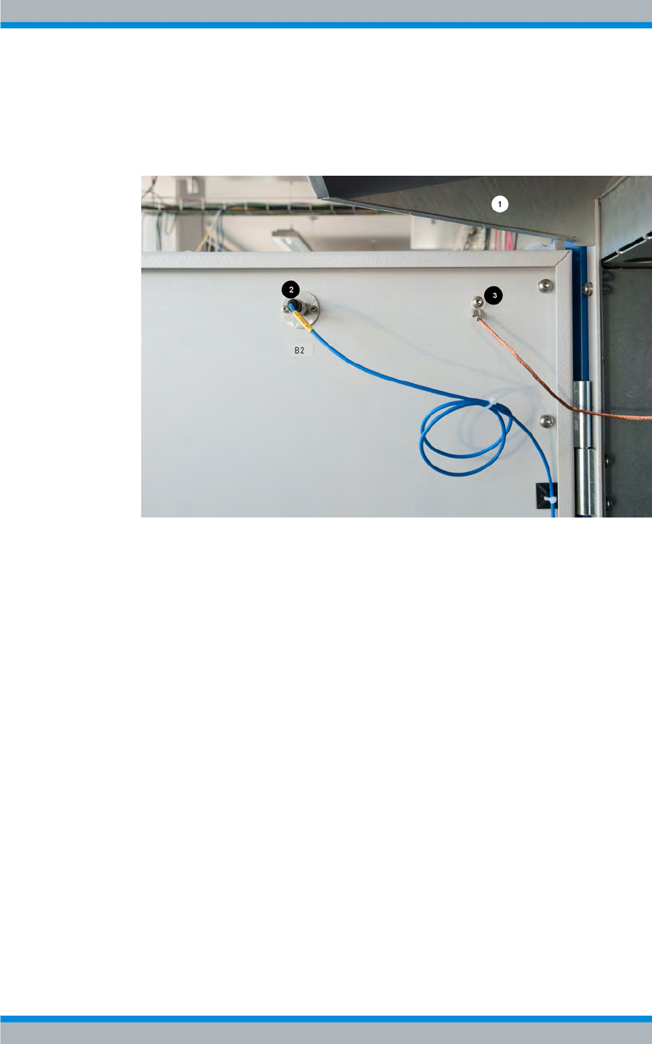
1. Unpack the rear door and hang it on the door hinges (item 2 in the following figure)
on the rear side of the rack.
2. Connect the potential equalization cable on the threaded bolt of the door (item 3) and
on the left wall of the rack (Torx screw)
Fig. 3-18: Exhaust Kit, Rear door of transmitter rack
1 = Exhaust air transfer duct, top
2 = Connection of temperature sensor B2
3 = Connection of potential equalization cable (Torx screw)
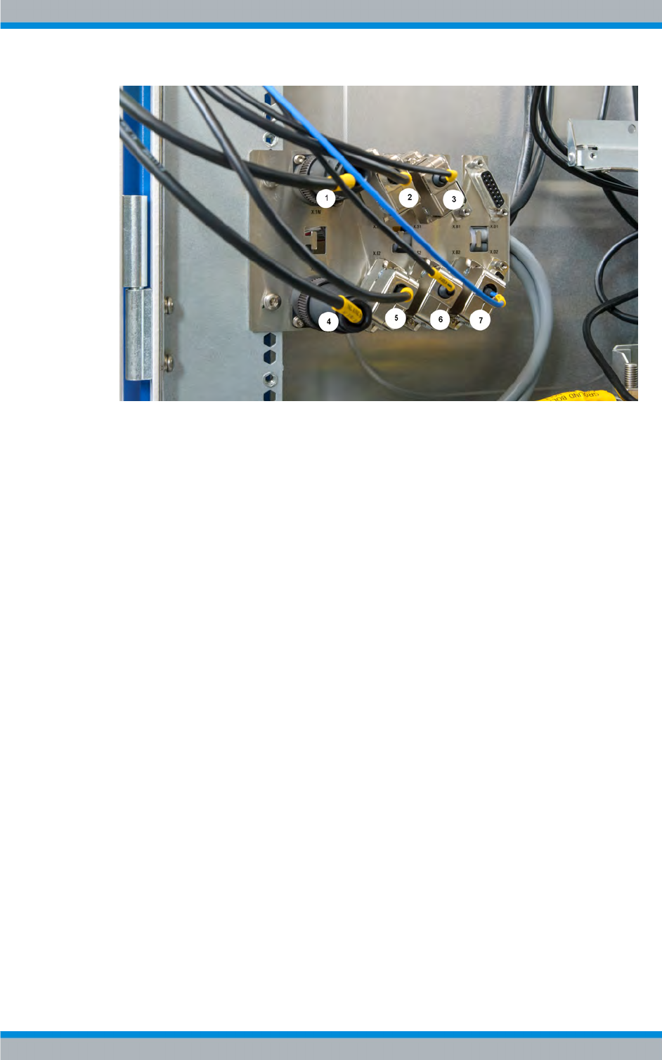
3. Attach the connecting cables for E1, E2, S1, S2, B1, and B2 to the connection panel
at the bottom of the left wall of the rack as followed.
● Power cable W.1N for fan E1 to X.1N
●Control cable W.E1 for fan E1 to X.E1
● Connection cable W.S1 for pressure sensor S1 to X.S1
● Power cable W.2N for fan E2 to X.2N
● Control cable W.E2 for fan E2 to X.E2
● Connection cable W.S2 for pressure sensor S2 to X.S2
● Connection cable W.B2 for temperature sensor B2 to X.B2
Installation R&S TMU9
Transmitter System R&S TMU9
R&S® TMU9
65System Manual 2600.5423.02 ─ 01
Fig. 3-19: Connection panel for exhaust kit.
1 = Power supply for fan E1 (X.1N)
2 = Connection of control line of Fan E1 (X.E1)
3 = Connection of pressure sensor S1 (X.S1)
4 = Power supply for fan E2 (X.2N)
5 = Connection of control line of Fan E2 (X.E2)
6 = Connection of pressure sensor S2 (X.S2)
3.3 Commissioning R&S TMU9
Commissioning of the transmitter system is described in the following document.
R&S THU9/TMU9 Transmitter System Operating Manual, Mat. No. 2109.9110.02
Commissioning R&S TMU9

Transmitter System R&S TMU9
R&S® TMU9
66System Manual 2600.5423.02 ─ 01
Commissioning R&S TMU9

Exciter/Transmitter Control R&S TCE900
R&S® TMU9
67System Manual 2600.5423.02 ─ 01
4 Exciter/Transmitter Control R&S TCE900
4.1 Design and Function R&S TCE900
4.1.1 R&S TCE900 General Design
The R&S TCE900 consists of a base module and various plug-in modules that enable
the following versions of the R&S TCE900.
●R&S TCE900 SystemControl (TCE900 SysCtrl)
●R&S TCE900 Exciter (TCE900 Exc)
R&S TCE900
The basic R&S TCE900 unit is the same for all versions and consists of the following
modules:
●Processor board (IPS1)
The IPS1 processing unit has the following properties:
–1.6 GHz INTEL ATOM N processor
– 2 GB RAM
–CR2032 (3 V) battery for supplying the realtime clock with power in the event of
a power failure.
– Linux-based R&S TCE900 software
A 4GB flash disk is located on the processor board; the operating system and all of
the system settings are saved on it.
The following interfaces are on the rear of the IPS1 unit:
– 2 x USB 2.0 for connecting external devices (mouse, keyboard, USB stick)
– 1 x Gigabit Ethernet 1000BaseT for externally controlling the R&S TCE900 via
SNMP, VNC or remote desktop
– 1 x DVI-D for connecting an external DVI-D monitor
The IPS1 board also provides internal interfaces (via internal system connector #1).
– 3 x PCIe 1.0a, Port A is used in the R&S TCE900 for exchanging data (TS or IP)
between the option module and the computer. The other two PCIe interfaces are
not used.
Furthermore, there are additional internal interfaces for special applications:
– 1 x SATA, interface (not used)
– 1 x +5 V, hard disk power supply (not used)
– 1 x mSATA socket for a 4GB flash disk (with operating system and system set-
tings)
●System connection board (SCB)
Design and Function R&S TCE900
Exciter/Transmitter Control R&S TCE900
R&S® TMU9
68System Manual 2600.5423.02 ─ 01
The system connection board is the central board of the R&S TCE900 with a con-
nection socket to the IPS1 processing unit (X17). The connector plugs for the back-
plane (X50, X51) are opposite the IPS1 connection socket.
The system connection board provides the following functions:
– The +12 V open-circuit voltage of the power supply is connected to the system
connection board via the X1, X2 and X3 interfaces. All modules of the R&S
TCE900 are supplied with a voltage of 12 V from there.
– FPGA D34 with PCIe interface for the IPS1 processing unit. This is used for
transferring central control tasks, e.g. fan control.
– PCIe switch D28 for distributing one IPS1 PCIe lane to the 5 modular units on the
backplane.
– USB hub D42 for distributing one IPS1 USB channel to the 5 modular units on
the backplane.
– Smart card adapter X12 with USB interface for managing options.
– Ethernet switch D25 for additional network interfaces in the instrument.
– GPS receiver K1 with USB interface. The antenna signals travel from the external
SMA input socket, "GPS ANT", to the GPS receiver via a cable. The GPS receiver
generates an internal 1 pps signal for monitoring DVB-T SFN networks.
●Power supply
●Fans
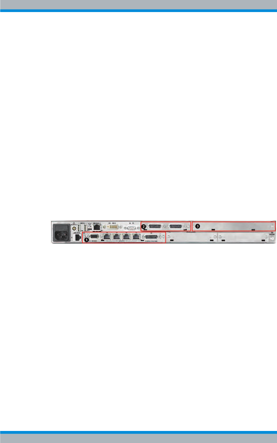
R&S TCE900 SysCtrl
Fig. 4-1: R&S TCE900 Control - rear view
1 = Tx interface
2 = Cooling Interface / Air Cooling Interface
3 = Ethernet switch (opt. for N+1 systems)
In addition to the basic unit, the R&S TCE900 SysCtrl contains the following plug-in mod-
ules:
●Tx interface
The TxIF in the R&S TCE900 is used as an interface from the IPS1 processor board
to the mains distribution unit and in specific systems to control an RF switch and to
monitor a switch-over panel. Additionally, there is an ethernet switch available, which
is used for the commumication to the exciters.
The TxIF is connected to the backplane via connection X100 (90-pin Airmax con-
nector).
The following connections are located on the rear panel:
– X44: Interface for the mains distribution unit (15-pin)
– X40-X43: 4 Ethernet interfaces (Gbit) for connecting the transmitter system's
devices
– X45: Interface to the RF switch and to a specific patch panel (15-pin)
●Air cooling interface (ACIF)
The air cooling interface is an optional card for the R&S TCE900.
Design and Function R&S TCE900
Exciter/Transmitter Control R&S TCE900
R&S® TMU9
69System Manual 2600.5423.02 ─ 01
For a medium-power transmitter, the connection from the exhaust kit to the trans-
mitter's control unit is established via the air cooling interface. This can be used to
control 2 fans independently of each other using a 0 V to 10 V voltage signal. Simul-
taneously, 2 tachometer signals from the fans can be evaluated to determine their
speed.
Two differential pressure sensors (1) are used to measure the pressure inside the
frame enclosure with reference to the outside air pressure. Through the ACIF of the
R&S TCE900, the RPM of the two fans (2) are regulated with the aim of maintaining
normal air pressure within the enclosed frame.
Two examples for controlling of the normal air pressure in the rack:
– For example, when the temperature of the air fed to the transmitter rises, the RPM
of the amplifier cooling fan will increase accordingly in order to adequately cool
the amplifier. As a result, the pressure within the enclosed frame will increase
and the ACIF will increase the RPM of the fans in the exhaust kit.
– When the temperature of the air fed to the transmitter decreases, the RPM of the
amplifier cooling fan will decrease. As a result, the pressure within the enclosed
frame will decrease and also the RPM of the fans in the exhaust kit.
During the initial commissioning of the system, a fallback RPM setting is configured.
This setting ensures that adequate cooling of the transmitter is ensured, even if the
ACIF goes off-line.
The air cooling interface is connected to the R&S TCE900 via USB on the backplane.
In addition to this, interrupt lines are also provided, which run as a signal line
(IRQSCB_OX, GPIO_OPTX_3) from the air cooling interface to the SCB/IPS1 and
run as feedback lines (GPIO_OPTX_4, F0_1PPSSCB_OX) from the IPS1/SCB to the
air cooling interface.
The plug position of the air cooling interface can be determined in the R&S TCE900
using SLOT_IDX.
●LAN switch
Additional Ethernet connections are provided using a LAN switch.
In addition, connections for the R&S TDU900 display unit and additional external instru-
ments (e.g. parallel remote control interface) are located here.
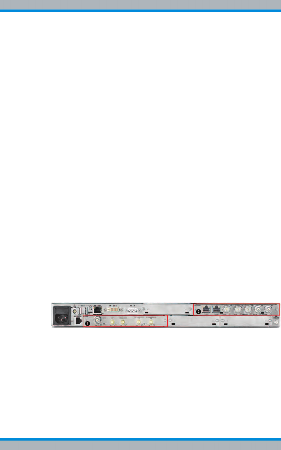
R&S TCE900 Exc
Fig. 4-2: R&S TCE900 Exciter - rear view
1 = RF Board
2 = Coder board
In addition to the basic unit, the R&S TCE900 Exc contains the following plug-in modules:
●Coder board
The coder board in the R&S TCE900 is used for the transport stream's (TS) baseband
coding. Depending on the standard in use, there are different models distinguished
by how the FPGAs are equipped.
The coder board is connected to the backplane using three Airmax connectors, X1
(90-pin), X2 (90-pin) and X3 (54-pin).
Design and Function R&S TCE900

Exciter/Transmitter Control R&S TCE900
R&S® TMU9
70System Manual 2600.5423.02 ─ 01
The following connections are located on the rear panel:
– X30/X31: Ethernet interface for TS via LAN
– X20/X21: BNC connections for TS via ASI
–X22: BNC connection for TS monitoring output
– X23: BNC connection for feeding in an external 1 pps pulse
– X24: BNC connection for outputting a reference signal (1 pps or 10 MHz)
●RF board
The RF board in the R&S TCE900 fulfills the following functions:
– Converting baseband data from digital to analog and converting modulation to
the final frequency (forward path).
– Adaptive precorrection and signal analysis of the baseband data extracted this
way (backward path).
– Central creation and distribution of the system cycle.
The RF board is connected to the backplane via connection X10 (90-pin Airmax con-
nector) and receives the digital baseband data from the coder over this connection.
JTAG interface X2 is provided for diagnostic purposes.
The following connections are located on the rear panel:
– X60: RF output (QMA)
– X61: RF output monitor (SMA)
– X64: Input for reference frequency (BNC)
– X67/X68 RF traceability for precorrection (QMA)
A GPS receiver can also be activated.
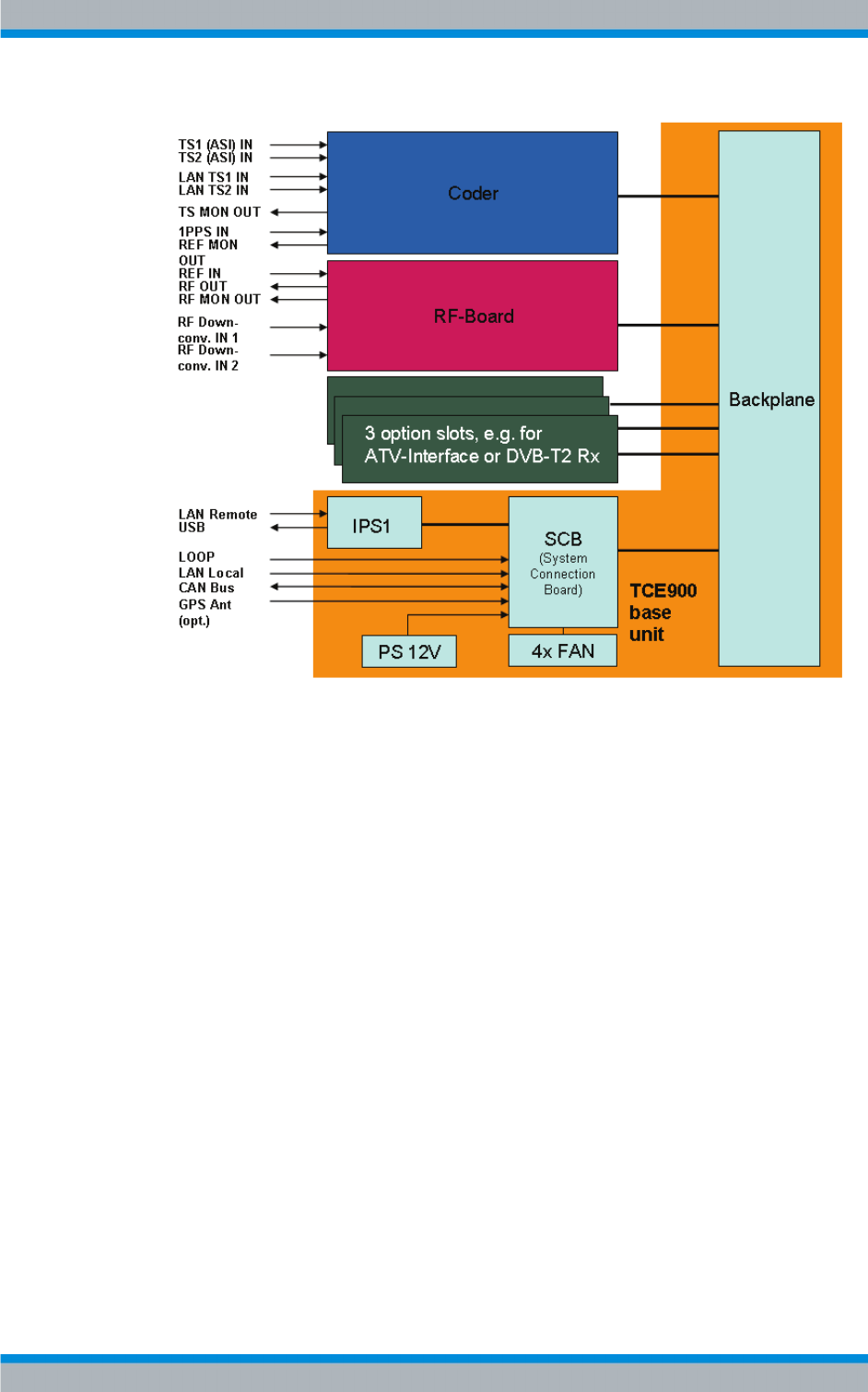
The general block diagram for the R&S TCE900 unit is below.
Design and Function R&S TCE900
Exciter/Transmitter Control R&S TCE900
R&S® TMU9
71System Manual 2600.5423.02 ─ 01
Fig. 4-3: R&S TCE900 block diagram
4.1.2 R&S TCE900 Functions
The individual versions of the R&S TCE900 perform the following functions:
R&S TCE900 SysCtrl
The R&S TCE900 SysCtrl takes over communications with the outside world and pro-
vides the connection to the R&S R&S TDU900.
R&S TCE900 Exc
The R&S TCE900 Exc takes over the tasks of an exciter, processes the data transport
stream and encodes the extracted data packets. The DTV signal is then precorrected,
modulated to the transmission frequency and forwarded to the transmitter output stage.
Design and Function R&S TCE900

Exciter/Transmitter Control R&S TCE900
R&S® TMU9
72System Manual 2600.5423.02 ─ 01
Design and Function R&S TCE900

Amplifier R&S PMU901
R&S® TMU9
73System Manual 2600.5423.02 ─ 01
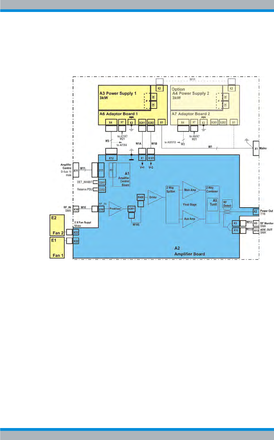
5 Amplifier R&S PMU901
5.1 Design and Function R&S PMU901
5.1.1 Device Purpose and Overview
The R&S PMU901 amplifier is a broadband unit that operates as a power amplifier in the
frequency range from 470 MHz to 862 MHz with the following TV standards:
●digital (DTV) standards: DVB‑T/H, DVB‑T2, ATSC, ATSC Mobil, ISDBTB
●analog (ATV) standards: ATVc (combined) B/G, D/K, K1, M/N, I, I1
It is based on the BLF888 transistor from NXP. The entire RF circuitry is on the A2 module
(amplifier board).
Broadband and Doherty mode (DTV only)
Apart from conventional broadband mode, the amplifier can also be operated according
to the Doherty principle in order to considerably improve AC efficiency (approx. 35 %).
Whereas the amplifier in the classic operating mode (as a linear amplifier with class AB
output stage) operates as a broadband unit without the need for adjustment across the
entire UHF range at AC efficiency levels around 25 %, the amplifier in Doherty mode is
band‑limited at efficiency levels > 35 %.
The operating mode of the amplifier is set using a tuning unit ("tunit") which can be
accessed from outside and is part of the top cover. With the tunit in its normal installation
position, the R&S PMU901 operates in AB mode as a conventional broadband linear
amplifier with 6 parallel‑connected BLF888 units. When turned through 180°, the tunit
allows the output stage to operate according to the Doherty principle. Three BLF888 units
then serve as the main amplifier and three as the auxiliary amplifier of the 6 dB Doherty
system. The tuning of the tunit now determines the available frequency range. There are
seven fixed tuning ranges or tunit variants for the entire UHF band (470 MHz to 862 MHz).
One tuning range covers up to 12 channels.
This special patented architecture of the R&S PMU901 means that the amplifier itself
actually remains invariant. Different variants do not need to be made available as replace-
ment parts. Every amplifier can be used in every transmitter. If a (Doherty) amplifier needs
to be replaced, the tunit is pulled out of the amplifier to be replaced and then inserted into
the replacement amplifier. If the frequency of the entire transmitter has to be changed
(very rare), only the tunits have to be changed (not necessary in all cases). If in doubt,
the amplifiers of a transmitter can of course always be configured to conventional broad-
band mode by turning the tunit. This operating mode is indispensable, especially in the
case of replacement transmitters in N+1 systems.
A control word is used to inform the amplifier control board of the installation position of
the tunit and therefore the operating mode. In Doherty mode, the control word also
informs the amplifier control board of the tuning range. If the tunit does not match the
Design and Function R&S PMU901

Amplifier R&S PMU901
R&S® TMU9
74System Manual 2600.5423.02 ─ 01
frequency of the transmitter or the wrong operating mode is configured, the amplifier
remains switched off and signals FREQ_FAIL.
Control and monitoring
The amplifier is operated via the transmitter control unit only. Module A1 (amplifier control
board), which operates independently of power and frequency band and is also used in
other TX9 amplifiers, is responsible for the monitoring and control functions as well as
CAN bus connection. The interface for the amplifier control board is largely compatible
with the VH8xxx amplifiers. This means that the amplifier can be operated using the
control unit from the 8000 family and outside of the transmitter for test purposes using
the GT800A1 test box.
Power supply
The amplifier has a 3 kW power supply unit (regular power supply unit 1) which delivers
both the amplifier operating voltage and the 15 V auxiliary voltage. As an option, an
identical power supply unit can be parallel‑connected as an active standby. Both power
supply units can be replaced without the amplifier needing to be switched off or removed
from the transmitter. The standby power supply unit can be assigned to a separate phase
on the system side. The permissible mains voltage range of the amplifier is 170 V to
264 V AC.
At reduced output powers, the efficiency of the amplifier can be optimized by reducing
the DC voltage of the power supply.
5.1.2 Mechanical Design
The amplifier is fully enclosed in a 19" metal housing. The height of the cabinet is 3.5 HU
(156 mm). The housing consists of a mounting frame, top cover, front cover and rear
panel. The two fans are attached to the rear panel. At the center of the housing is the
amplifier board, under which is the heat sink and under that the power supply unit with
power adaptor board.
After the mains voltage has been disconnected (after the pre‑trip has been switched off),
the amplifier can be removed from the rack without disconnecting any connectors while
the transmitter is still in operation (self-engaging plug‑in connections).
Although the R&S PMU901 amplifier is normally used in combination with a transmitter
rack, it can also be operated as a stand‑alone desktop unit together with the R&S TCE900
exciter.
Modules
The amplifier consists of the following modules:
●A1: Amplifier control board
●A2: Amplifier board
●A3, A4: Power supply 1, power supply 2 (standby, optional)
●A5: Tunit (tuning unit)
Design and Function R&S PMU901
Amplifier R&S PMU901
R&S® TMU9
75System Manual 2600.5423.02 ─ 01
●A6, A7: Adaptor board 1, adaptor board 2 (standby)
The entire amplifier unit is on the top side of the amplifier.
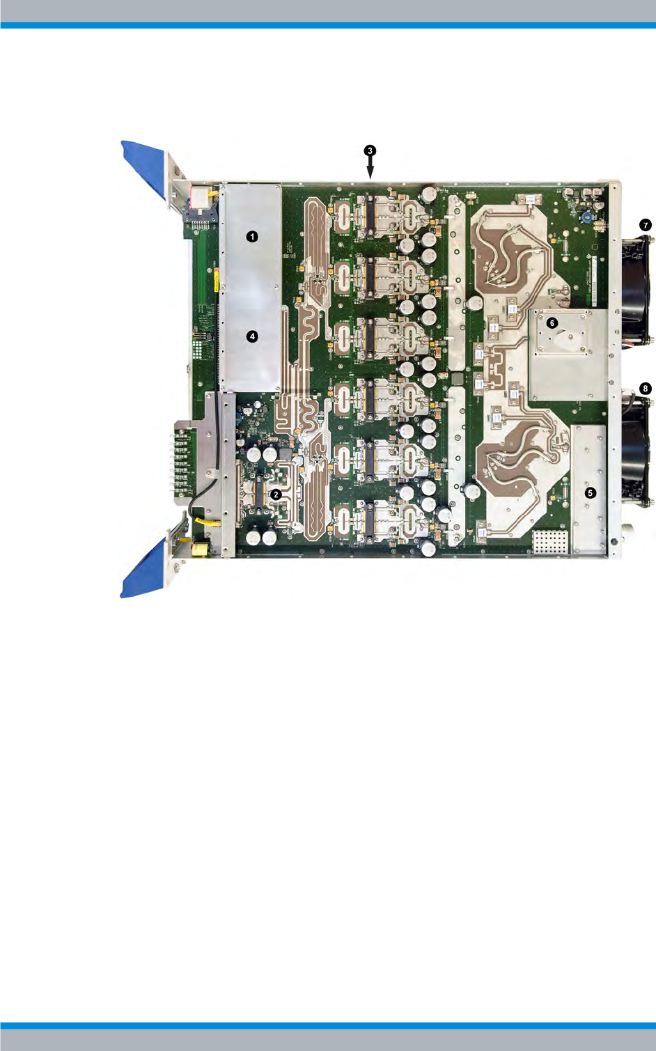
Fig. 5-1: Amplifier board
–
A2 (top cover removed)
1 = Preamplifier
2 = Driver amplifier
3 = Output stage with 6 transistors
4 = Amplifier control board – A1
5 = RF detectors
6 = Tunit – A5 (here in normal installation position for broadband mode)
7 = Fan 1
8 = Fan 2
One or two power supply units are in the lower part of the amplifier behind the front cover.
Design and Function R&S PMU901
Amplifier R&S PMU901
R&S® TMU9
76System Manual 2600.5423.02 ─ 01
Fig. 5-2: Power supply unit and heat sink (front cover removed)
1 = Fins of heat sink
2 = Power supply 1 – A3
3 = Installation compartment for power supply 2 – A4 (option)
One or two power adaptor boards are on the underside of the amplifier behind the PAB
cover.
Fig. 5-3: Power adaptor board (cover removed)
1 = Power adaptor board 1 – A6
2 = Installation location for power adaptor board 2 – A7 (option)
3 = Fan 1
4 = Fan 2
Cooling
The amplifier is cooled by a high‑performance copper heat sink and two dedicated ampli-
fier fans. The cooling system features the following:
●The amplifier circuitry is cooled by means of thermal conduction to the heat sink which
dissipates heat to the flow of cooling air inside the amplifier (no additional fans are
used).
Design and Function R&S PMU901
Amplifier R&S PMU901
R&S® TMU9
77System Manual 2600.5423.02 ─ 01
●The power supply unit has its own heat sink which also dissipates heat from the power
supply unit to the flow of cooling air inside the amplifier.
●Part of the cooling air also flows through the power supply unit circuitry in order to
cool the components.
Tunit
The installation position of the tuning unit ("tunit") determines whether the two groups of
three identical output‑stage transistors are parallel‑connected to form a classic broad-
band amplifier or whether they form a Doherty system with a main and auxiliary amplifier.
●With the tunit in its normal installation position ("B‑Mode" on the top cover), the
amplifier functions as a conventional linear amplifier with 6 parallel‑connected out-
put‑stage transistors in AB mode. It thus operates as a broadband unit without the
need for adjustment across the entire UHF range.
●When turned through 180° ("D‑Mode" on the top cover), the tunit allows the output
stage to operate according to the Doherty principle. Three output‑stage transistors
then serve as the main amplifier and three as the auxiliary amplifier of the 6 dB Doh-
erty system. In this operating mode, the two tuning elements of the tunit determine
the operating frequency(-ies) of the amplifier. They are indicated on the tunit label
and are only valid for as long as the calibration sticker is undamaged.
The tunit is inserted from above into the cover of the amplifier section in the amplifier. It
is therefore only accessible when the amplifier has been removed from the transmitter.
The amplifier must be switched off before the tunit is removed! Removal while the ampli-
fier is still in operation can result in the transistors being irreparably damaged.
5.1.3 Display Elements and Interfaces
5.1.3.1 LEDs and Test Point – Front Panel
The following LEDs for indicating states and faults are on the front panel:
Design and Function R&S PMU901

Amplifier R&S PMU901
R&S® TMU9
78System Manual 2600.5423.02 ─ 01
Name No. Signaling Meaning
AMPLIFIER ON H1 LED, green The LED lights up when the
amplifier is ready for operation,
i.e. the supply voltage is present
and the transmitter is in opera-
tion.
LINK H2 LED, green Amplifier communication with the
BUS.
●Flashing rapidly: No master
●Flashing slowly: Not opera-
tional but communication
link present
●Permanently lit: Normal
communication
●OFF: Processor is not being
supplied with power (no
V_AUX)
RF IN FAIL H3 LED, yellow The LED lights up if the RF input
level (X10) is below the preset
threshold.
MUTE H4 LED, yellow The RF output signal (X1) is sup-
pressed (caused by the
SHUT_DOWN command, if the
external power combiner over-
heats, with the RF_IN_FAIL mes-
sage or with the RF_MUTE sig-
nal).
REFLECTION H5 LED, yellow The LED lights up if the reflection
at the RF output exceeds a
threshold. The message is stored
in a nonvolatile memory in the
amplifier and can be reset at the
transmitter control unit (Reset).
RF POWER FAIL H6 LED, red The LED lights up if the RF output
power is below half (-3 dB) of the
nominal value.
TEMP FAIL H7 LED, red The LED lights up in the case of
overtemperature in the amplifier
unit. The message is stored in a
nonvolatile memory in the CAN
controller and can be reset at the
transmitter control unit (Reset).
The output power is suppressed
for as long as overtemperature
exists.
TRANSISTOR FAIL H8 LED, red The LED lights up if a transistor
fails in the output stage or driver.
FAN FAIL H9 LED, yellow The LED lights up if one or more
fans fail.
Indication of other operating states:
●H6 – H8 flash
Design and Function R&S PMU901
Amplifier R&S PMU901
R&S® TMU9
79System Manual 2600.5423.02 ─ 01
A problem has occurred during initialization. Certain hardware conditions are not ful-
filled, e.g.:
– Internal operating voltages are missing.
– The tunit installed in the transmitter does not correspond to that expected by the
transmitter (returned FREQ_ID).
– No FREQ_ID has yet been returned by the transmitter.
●H3 – H5 chaser light
Bias adjustment is active (duration: approx. 2 min.).
●H1 to H8 flash for 10 s
The command to detect an amplifier has been activated
The generated status displays and measurement values are shown in the GUI of the
transmitter control unit (R&S TDU900).
Front RF test connector
At the RF MONITOR test point (X3, SMA socket), part of the output signal from the
amplifier circuitry is output via a directional coupler (1 V test point). This allows evaluation
of the signal quality downstream of the amplifier.
The coupling attenuation of the RF MONITOR test point has a frequency response of
-6 dB per octave. The attenuation at 650 MHz is stored and can be queried via the trans-
mitter control unit. The level at X3 changes slightly (approx. 0.1 dB) if a connection is
disconnected or connected at X13 (ADE OUT, rear panel).
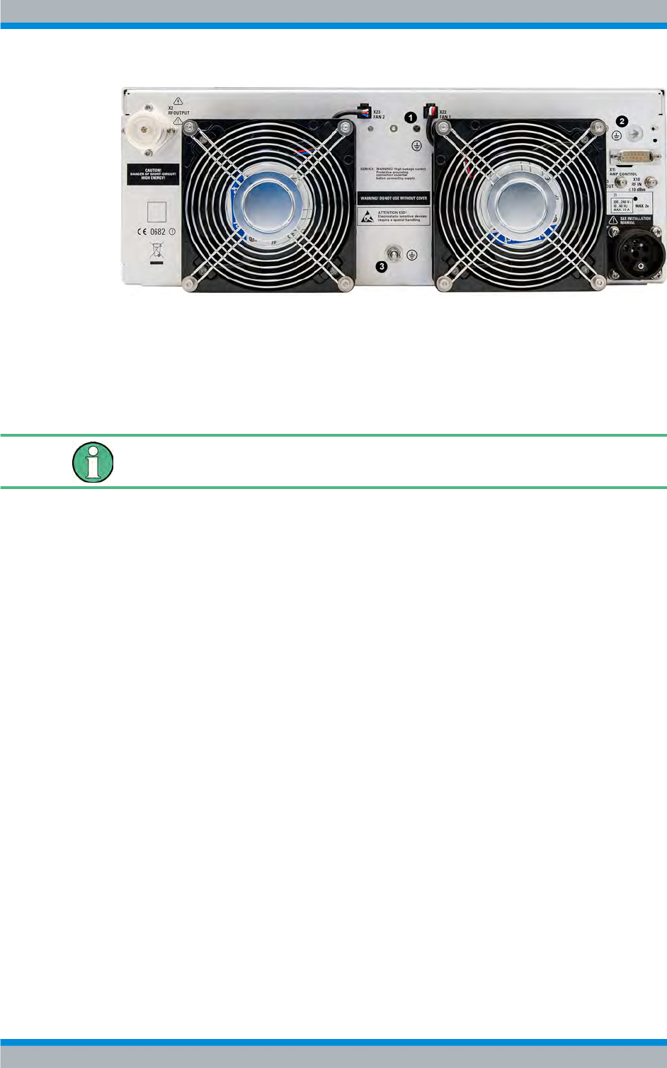
5.1.3.2 Connectors – Rear Panel
The following connectors are on the rear panel of the amplifier:
●X1 – Mains voltage feed for 1 or 2 power supply units
●X2 – HF output RF OUT(7/16 female connector)
●X10 – HF input RF IN(SMA female connector)
●X11 – AMPLIFIER CONTROL interface to the amplifier control board with integrated
connection to the CAN bus (D‑Sub male connector, 15‑contact)
●X13 – Second ADE OUT RF test connector for connecting the ADE demodulator for
automatic digital precorrection upstream of the channel bandpass filter (with 1 ampli-
fier in the transmitter; SMA female connector)
●X22, X23 – Connection for fan 1 and fan 2 (Molex male connector)
●3 connection possibilities for the additional PE conductor (a second PE conductor is
always required!)
Design and Function R&S PMU901
Amplifier R&S PMU901
R&S® TMU9
80System Manual 2600.5423.02 ─ 01
Fig. 5-4: Rear panel of R&S PMU901 with connections for a second PE conductor
1 = Threaded hole (M6) for screwing on a ground cable with cable lug (alternative to 3)
2 = Multilam female connector for self‑engaging connection of second PE conductor in transmitter rack
3 = Ground bolt (M5) for connection of second PE conductor at test station
Amplifier control
All control functions in the TX9 transmitters are executed by means of CAN commands
via the X11 interface.
Design and Function R&S PMU901
Amplifier R&S PMU901
R&S® TMU9
81System Manual 2600.5423.02 ─ 01
5.1.4 Circuit Descriptions
5.1.4.1 Block Diagram
Fig. 5-5: Block diagram of R&S PMU901
5.1.4.2 Signal Gain in Preamplifier and Driver
The entire signal gain process takes place on the amplifier board (module A2). It goes
though the following steps in the preamplifier and driver.
●The RF input signal passes from the amplifier input X10 on the rear panel of the
instrument along the RF line W10 and into the preamplifier, which is under an
RF‑shielded cover.
●In the preamplifier, the signal passes through the following components in sequence:
– Amplitude regulator
– Small‑signal amplifier
– Phase regulator
●This is followed by an LDMOS transistor stage (BLF642, single‑ended, A mode) as
a preliminary driver.
Design and Function R&S PMU901
Amplifier R&S PMU901
R&S® TMU9
82System Manual 2600.5423.02 ─ 01
●The signal leaves the preamplifier and is fed to the input of the driver amplifier via the
cable W145x. This input consists of two single‑ended LDMOS transistor stages which
are interconnected by means of 90° jumpers. The two transistor halves of the
BLF888B push‑pull transistor are used for this purpose.
●The cable W145x is also used for phase adjustment (in the case of design modifica-
tions or for tolerance adjustment). It connects the connectors X301 and X400.
●The output signal of the driver is fed to the output‑stage splitter via a harmonic filter.
This filter is used especially at low frequencies to suppress the first harmonic.
The cable W145x must not be removed and should only be replaced with a cable with
the same R&S part number. Failure to observe this point can result in destruction of
absorbers of the power combiner in the transmitter (if more than one amplifier is installed).
5.1.4.3 Signal Gain in Doherty-Capable Output Stage
The output stage is divided into two groups, each with three transistors. In Doherty mode,
one group forms the main amplifier (3 x BLF888B) and the other forms the auxiliary
amplifier (3 x BLF888A). If the two groups have equal priority, however, they can also
form a conventional output stage.
The following steps take place in the output stage:
●The output signal of the driver is fed via a 90° splitter to two output‑stage groups each
with three transistors.
●The two power streams are divided between the three transistors of each out-
put‑stage group via a 0° splitter. The output‑stage group which forms the main ampli-
fier in Doherty mode uses BLF888B transistors, and the output‑stage group for the
auxiliary amplifier uses BLF888A transistors.
●Two 0° combiners combine each group of three partial power streams and make them
available at the inputs of a 2‑way power combiner ready for addition.
●The tunit connected at the power combiner determines the operating mode of the
amplifier:
– Conventional broadband AB mode in the normal installation position
– Doherty mode if the tunit is turned through 180°
●Directional couplers upstream of the RF output of the amplifier (downstream of the
2‑way power combiner) detect forward and reflected power. Their signals are fed to
RF detectors. A further directional coupler provides two free decoupled RF test points
(RF MONITOR, ADE OUT) via a small splitter.
The operating points of the transistors of the main and auxiliary amplifier can be set
separately. In Doherty mode, the main amplifier operates in AB mode and the auxiliary
amplifier in C mode. When the amplifier operates as a conventional broadband amplifier,
all of its output‑stage transistors operate in AB mode.
Design and Function R&S PMU901

Amplifier R&S PMU901
R&S® TMU9
83System Manual 2600.5423.02 ─ 01
5.1.4.4 Power Control
To ensure that the required power is always present at the amplifier output, the level
tolerances at the following points are adjusted by means of a power control circuit.
●at the amplifier output
●at the entire RF amplifier stage
During power control, a control amplifier which is on the amplifier board (module A2,
preamplifier section) is supplied with an actual voltage and a nominal voltage. The nom-
inal voltage is the VREF_PWR signal which is fed as a CAN command and is used to
adjust the output power.
Intelligent control brake
In the case of the R&S PMU901 with the special output‑stage architecture necessary for
the Doherty operating mode, it is not possible to apply the control principle with transis-
tor‑failure tolerance which is traditionally used at Rohde & Schwarz and features two
independent actual value detectors downstream of the subamplifiers with the same out-
put power.
The PWR_OUT signal which is proportional to the sum output power is used as the actual
value for control. In order to still retain tolerance with regard to transistor failures, the
principle of the "intelligent control brake" is applied (IPLIM = Intelligent Power LIMiter).
Here, the adjustment range of the control amplifier is simply limited adaptively in such a
way that overloading of the intact transistors in the event of a transistor failure cannot
result in their failure. The control brake therefore always adapts to the current conditions
in the control circuit. This principle exploits the fact that changes in gain and input signal
which are the result of temperature and aging take place only slowly.
The manipulated variable (the regulating voltage of the PIN attenuator) is recorded at
long intervals. The control brake (i.e. the maximum possible value for the regulating volt-
age) is derived from the measured value plus the difference which is not exceeded until
the next measurement, provided that normal temperature and aging processes exist. This
means that the control brake will also increase slowly if, for example, the gain drops with
increasing temperature and the regulating voltage of the PIN attenuator increases in order
to maintain the output power. In the case of dramatic changes resulting from transistor
failure or dramatic changes in the input signal, adaptation of the control brake with respect
to this is stopped and the control brake thus becomes fully effective.
The amplifier control now analyzes the current situation without disturbance and
responds according to the determined cause. If the cause is, for example, a transistor
failure, the amplifier control adapts the nominal regulation value according to the remain-
ing performance of the amplifier. In this way, a stabilized condition is achieved, albeit with
reduced output power. At power ON and if the nominal regulation value is changed, the
control brake is of course stopped briefly.
Reflected power test point
In the case of reflection at the amplifier output, the forward power is reduced in order to
protect the amplifier. For this purpose, the REFL_SAVE signal is acquired at the reflected
power test point. This signal is superimposed on the actual value signal during power
control by means of a diode. If the REFL_SAVE signal exceeds the voltage of the forward
Design and Function R&S PMU901

Amplifier R&S PMU901
R&S® TMU9
84System Manual 2600.5423.02 ─ 01
power detector PWR_OUT, the reflected power test point takes over power control. The
control amplifier supplies the control voltage V_REG as the output quantity and this volt-
age is fed to the amplitude regulator in the preamplifier.
Additionally, the REFL_OUT signal is acquired at the reflected power test point. This
signal together with the PWR_OUT signal (forward power) is used for VSWR indication
at the amplifier output.
5.1.4.5 Self‑Protection Mechanisms
The amplifier has a series of self‑protection and monitoring mechanisms which protect it
against irreparable damage in the case of impermissible operating conditions and enable
transmission to continue for as long as possible. The following mechanisms are available.
●Power supply monitoring
●Input level monitoring
●Output power limitation
●Temperature monitoring incl. fan control
●Reflection monitoring
●Operating mode monitoring
Power supply unit monitoring
The power supply unit has the following self‑protection mechanisms:
●Overtemperature shutdown for the duration of overtemperature
●Short‑circuit current limitation
●Input voltage monitor (enables shutdown to limit the input current in the case of
undervoltage)
●Overvoltage limitation (on DC side)
If no standby power supply unit is installed, failure of the power supply unit (/
DC_OK = high) will mean failure of the amplifier. If a standby power supply unit is installed,
there will be no operational restrictions. The amplifier will however be completely deac-
tivated if both power supply units fail.
The overtemperature shutdown in the power supply is intended purely as a self‑protection
mechanism only and is not indicated by the front LED as the DC voltage is switched off.
A temperature shutdown at the power supply is signaled only indirectly by the message /
DC_OK_x. The power supply unit has status LEDs for normal operation and fault indi-
cation. These LEDs are indirectly visible after removal of the front cover (and, where
applicable, the air filter).
Input level monitoring
If the input level drops below a defined threshold (RF_IN_FAIL), power control is influ-
enced by the following measures:
●The amplitude regulator for power control is switched to maximum attenuation
●The internal reference voltage for power control is suppressed
Design and Function R&S PMU901

Amplifier R&S PMU901
R&S® TMU9
85System Manual 2600.5423.02 ─ 01
A soft start is performed as soon as the input signal returns. The selected threshold is
such that the amplifier can be reliably operated across the entire temperature range in
all permissible operating modes, even at the lower tolerance limit of the RF_IN input
signal at X10.
Output power limitation
The output power is set by means of the VREF_PWR signal. The output power is limited
such that the amplifier cannot be damaged at excessively high VREF_PWR values. In
addition, the average output power of the amplifier is also limited by means of hardware.
Excessive power if the forward power test point fails as well as subsequent failures if a
transistor fails are countered by the intelligent control brake.
Temperature monitoring and fan control
The power supply units and amplifier circuit each have a dedicated hardware overtem-
perature shutdown mechanism. If a temperature threshold is exceeded, the amplifier is
disabled (TEMP_FAIL message), whereby the threshold for the overtemperature shut-
down is above the permissible operating temperature. This ensures that the remaining
overall power loss does not lead to overheating of the instrument, even with total failure
of the cooling system.
The fan has four different speed settings, whereby the second speed is the standard
speed which has been optimized with regard to the average junction temperature of the
output stage and to noise generation.
To ensure that transmission can continue for as long as possible, the temperature and
fan control functions work together as follows:
●If the temperature rises in the amplifier circuit, the fan speed is first increased before
the hardware shutdown threshold is reached.
●If this is not enough, at temperatures above 83 °C the amplifier control begins to
reduce the output power in steps of 1 dB (DTV only, REDUCED_PWR message).
●With ATV, the output power is not reduced at excessively high temperatures. Instead,
the amplifier is shut down by means of software at 85 °C.
●At temperatures above 90 °C, the amplifier remains switched off by means of hard-
ware for as long as the overtemperature exists. Overtemperature on the amplifier
board is indicated by means of the front TEMP FAIL LED (with ATV: at 85 °C and
higher).
●An appropriate hysteresis is integrated to prevent deactivation and activation from
occurring too soon. A soft start is performed as soon as power returns.
In addition, the inlet and outlet temperature is measured by means of two sensors (on
the front and rear side of the amplifier board, thermally insulated from the rest of the
printed board). This allows, for example, a fouled air filter to be detected and changed in
good time (AIR_FILT_FAIL message).
Reflection monitoring
A distinction is made between the following types of reflection monitoring (REFLECTION
message):
Design and Function R&S PMU901
Amplifier R&S PMU901
R&S® TMU9
86System Manual 2600.5423.02 ─ 01
●With major reflection above reflection threshold 2 (s = 2), the power is briefly cut off
completely first of all; a soft start is performed immediately afterwards. If any reflection
remains, the amplifier protects itself by reducing the output power. The time constant
selected for the shutdown is such that damage to the amplifier is prevented in the
case of total reflection and at all phase angles of the reflection at X2.
●With weaker reflection above reflection threshold 1 (S = 1.5), the output power is
reduced without preceding shutdown.
●When reflection no longer exists, the power reduction is canceled automatically.
Operating mode monitoring
Using a 5‑bit code (FREQ_ID), the transmitter notifies the amplifier of the expected oper-
ating mode and, in Doherty mode, the expected tuning variant (transmit frequency). If this
code is not the same as the code of the tunit installed in the amplifier, the amplifier ignores
the ON command and signals FREQ_FAIL.
For conventional broadband operation, the FREQ_ID is 00000. If no tunit is installed, the
amplifier signals FREQ_ID 11111. All other FREQ_IDs are reserved for Doherty mode.
5.1.4.6 Emergency Shutdown
The amplifier can be disabled externally by means of the SHUT_DOWN signal at X11,
for example to ensure self‑protection for the absorber of the power combiner in the trans-
mitter. The signal, which is immune to cable breaks, is fed via an optocoupler on
CAN_GND and is therefore insulated from amplifier ground. The output power is sup-
pressed for as long as no connection to CAN_GND exists.
To activate the amplifier when the R&S GT800A1 test box is being used, it is necessary
to connect X20 (GND) to X21 on the test box.
5.1.5 Specifications
5.1.5.1 General Data
Frequency range 470 MHz to 862 MHz (band 4 and 5)
Power supply (3 separate phases)
- Nominal voltage range 200 V to 240 V
- Tolerance range 170 V to 264 V
- Nominal frequency range 50 Hz to 60 Hz
- Tolerance range 47 Hz to 63 Hz
Power factor (cosφ)≥0.98 at nominal power
Design and Function R&S PMU901
Amplifier R&S PMU901
R&S® TMU9
87System Manual 2600.5423.02 ─ 01
Operating temperature range (Turoom) +1 °C to +45 °C
Inlet air temperature (Tinlet air) +1 °C to +45 °C
Storage and transport temperature range -40 °C to +85 °C
Setting range for amplifier phase (via CAN) ±12.5° to ±17.5°
Harmonics
- up to 550 MHz ≤ -30 dBc
- as of 550 MHz ≤ -50 dBc
VSWR RF input (X10) ≤ 1.4
VSWR RF output (X2)
- compliance with specifications ≤ 1.3
- reduction as of 1.6±0.3
Overtemperature shutdown 90 °C ±4 K (sensor on heat sink)
Permissible humidity ≤ 95 % at 40 °C, non‑cyclical, non‑condensing
Ambient conditions Complies with ETSI EN 300‑019‑1‑3
(V2.3.2 2009‑07) Class 3.2 with reduced ambient
temperature and humidity range
Maximum installation altitude above sea level 2000 m (higher on request; power supply units up to
3000 m)
Vibration, sinewave 5 Hz to 150 Hz,
max. 1.8 g at 55 Hz,
max. 0.5 g at 55 Hz to 150 Hz
in line with EN60068-2-6, EN61010-1
Vibration, random 10 Hz to 300 Hz
Acceleration 1.2 g (rms)
Shock Shock spectrum 40 g/11 ms to MIL‑STD 810E Method
No. 516.4
Dimensions (depth, width, height) 550 mm, 153 mm, 19'' (3.5 HU)
Weight < 25 kg
5.1.5.2 Digital TV (DTV)
Input power Pavgnominal (DVB‑T / ATSC) 0 dBm / 1 dBm
Maximum input power Pavg,in ≤ +13 dBm
Control range (DVB‑T / ATSC) -6 dBm to +6 dBm / +5 dBm to +7 dBm
Detector setting (signal PEAK_AV, X11) Low (AV)
Output power Pavgnominal (VREF_PWR = 4 V) 600 W
Design and Function R&S PMU901
Amplifier R&S PMU901
R&S® TMU9
88System Manual 2600.5423.02 ─ 01
Setting range for output power referenced to
Pavgnominal
-10 dB to +1.2 dB
Output power DVB‑T, Pavg (nominal value / maximum
value)
600 W / 700 W; Doherty: 600 W / 650 W*
Output power ATSC, Pavg (nominal value / maximum
value)
750 W / 750 W; Doherty: 600 W / 650 W*
Shoulder attenuation at Pavgnominal (without precor-
rection / with precorrection)
≥ +26 dB / ≥ +37 dB
MER with DVB‑T, Pavgnominal (shoulder precorrected
> 37 dB)
≥ 33 dB
Power consumption:
- at 230 V, DVB‑T, 650 W ≤ 3000 VA (Doherty: ≤ 2000 VA)
- at 230 V, ATSC, 750 W ≤ 3000 VA
* Depends on MER and channel
5.1.5.3 Analog TV (ATV Combined)
Input power Psyncnominal +3.5 dBm
Maximum input power Pavg,in ≤ +13 dBm
Control range Psync,in -2.5 dBm to +9.5 dBm
Detector setting (signal PEAK_AV, X11) High (PEAK)
Output power Psyncnominal (VREF_PWR = 4 V) 1000 W
Output power Pavg,max 675 W
Setting range for output power referenced to
Psyncnominal
-10 dB to +0 dB
Power consumption at 1000 W:
- at 230 V, APL = 0 % (all‑black picture) ≤ 3000 VA
- at 230 V, APL = 50 % (gray picture) ≤ 2400 VA
5.1.5.4 CW Mode
Input power Pavgnominal +1 dBm
Maximum input power Pavg,in ≤ +13 dBm
Control range Pavg,in -5 dBm to +7 dBm
Detector setting (signal PEAK_AV, X11) Low (AV)
Design and Function R&S PMU901

Amplifier R&S PMU901
R&S® TMU9
89System Manual 2600.5423.02 ─ 01
Output power Pavgnominal 675 W
Power consumption: at 230 V, CW, 600 W ≤ 2500 VA
Design and Function R&S PMU901

Amplifier R&S PMU901
R&S® TMU9
90System Manual 2600.5423.02 ─ 01
Design and Function R&S PMU901
R&S TMU9 Interface Description
R&S® TMU9
91System Manual 2600.5423.02 ─ 01
A R&S TMU9 Interface Description
A.1 External Transmitter Interfaces
A.1.1 Transmitter Input AC
Table 1-1: Q1: Supply input
Signal
Name/Description
Direc-
tion
Value range Connection
point
Remarks
Line L1 Input 230 V ± 15% Q1.2 230 V L-N
Line L2 Input 230 V ± 15% Q1.4 230 V L-N
Line L3 Input 230 V ± 15% Q1.6 230 V L-N
Neutral N Input 0 V Q1.8/N Neutral conductor
input N
Table 1-2: Q1: Protective conductor terminal
Signal
Name/Description
Direc-
tion
Value range Connection
point
Remarks
PROTECTION EARTH PE Input 0 V X.PE.1 PE terminal NVT
PROTECTION EARTH PE Input 0 V X.PE Station PE
The mains distribution unit designed for the TMU9 is limited to 230 V power supplies.
●AC power supply: 230 V; 2W + PE (L1/N/PE)
●AC power supply: 400 V / 230 V; 4W + PE (L1/L2/L3/N/PE)
All other network configurations can be covered by the optional use of the R&S ZR800Z10
mains distribution unit:
●AC power supply: 230 V; 2W + PE (L1/N/PE)
●AC power supply: 240 V; 2W + PE (L1/L2/PE)
●AC power supply: 400 V / 230 V; 4W + PE (L1/L2/L3/N/PE)
●AC power supply: 208 V Y; 3W + PE (L1/L2/L3/PE)
●AC power supply: 240 V Y; 3W + PE (L1/L2/L3/PE)
●AC power supply: 240 V delta; 3W + PE (L1/L2/L3/PE)
A.1.2 Input Signals (TS, RF, Reference)
The following interfaces are present again with each additional signal processing and
therefore are listed only once at the transmitter level.
External Transmitter Interfaces
R&S TMU9 Interface Description
R&S® TMU9
92System Manual 2600.5423.02 ─ 01
●With dual drive, another TS splitter (dual drive) is put upstream of the signal pro-
cessing modules (TCE900 exciter).
●With N+1 systems, a TS splitter (N+1) is put upstream of the signal processing mod-
ule(s) (TCE900 exciter) of the transmitter(s) TxA, and another ASI routing switch is
put upstream of the signal processing module(s) (TCE900 exciter) of the transmit-
ter(s) TxB.
TS feed (ASI, IP)
Table 1-3: X20 – TS1 in: BNC jack 75
Ω
Signal
Name/Description
Direc-
tion
Value range Connection
point
Remarks
TS1 Input ASI / SMPTE310M X20.1 TS1 input exciter
GND Bidirec-
tional
0 V X20.2 GND / shield
Table 1-4: X21 – TS2 in: BNC jack 75
Ω
Signal
Name/Description
Direc-
tion
Value range Connection
point
Remarks
TS2 Input ASI / SMPTE310M X21.1 TS2 Input Exciter
GND Bidirec-
tional
0 V X21.2 GND / shield
Table 1-5: X30 – TS1 LAN: 8-pin RJ-45 socket
Signal
Name/Description
Direc-
tion
Value range Connection
point
Remarks
TX+ Output Ethernet X32.1 Transmitting line
TX- Output Ethernet X32.2 Transmitting line
RX+ Input Ethernet X32.3 Receiving line
Bidirec-
tional
75 Ω termination X32.4
Bidirec-
tional
75 Ω termination X32.5
RX- Input Ethernet X32.6 Receiving line
Bidirec-
tional
75 Ω termination X32.7
Bidirec-
tional
75 Ω termination X32.8
External Transmitter Interfaces
R&S TMU9 Interface Description
R&S® TMU9
93System Manual 2600.5423.02 ─ 01
Table 1-6: X31 – TS2 LAN: 8-pin RJ-45 socket
Signal
Name/Description
Direc-
tion
Value range Connection
point
Remarks
TX+ Output Ethernet X33.1 Transmitting line
TX- Output Ethernet X33.2 Transmitting line
RX+ Input Ethernet X33.3 Receiving line
Bidirec-
tional
75 Ω termination X33.4
Bidirec-
tional
75 Ω termination X33.5
RX- Input Ethernet X33.6 Receiving line
Bidirec-
tional
75 ΩX33.7
Bidirec-
tional
75 ΩX33.8
Receiver module (optional)
Table 1-7: X69 – RF IN DVB-T2 Receiver: BNC jack 50
Ω
Signal
Name/Description
Direc-
tion
Value range Connection
point
Remarks
ANTENNA 1 Input 30 MHz to 1 GHz
-92 dBm to 0 dBm
75 Ω
X69.1 RF input
BNC jack
GND Bidirec-
tional
0 V X69.2
Reference feed
Table 1-8: X66 – GPS ANTENNA: SMA socket 50
Ω
Signal
Name/Description
Direc-
tion
Value range Connection
point
Remarks
GPS ANT Input -144 dBm to -5 dBm X66.1 50 Ω SMA socket
GND Bidirec-
tional
0 V X66.2
Table 1-9: X23 – 1PPS IN exciter: BNC jack 50
Ω
Signal
Name/Description
Direc-
tion
Value range Connection
point
Remarks
1PPS_EXTERN Input TTL level (pos.edge) X23.1 Seconds pulse from
external GPS
receiver
GND Bidirec-
tional
0 V X23.2 GND / shield
External Transmitter Interfaces
R&S TMU9 Interface Description
R&S® TMU9
94System Manual 2600.5423.02 ─ 01
Table 1-10: X64 – REF IN: BNC jack 50
Ω
Signal
Name/Description
Direc-
tion
Value range Connection
point
Remarks
REF IN Input -5.0 dBm to 20 dBm or
TTL
X64.1 50 Ω BNC jack
GND Bidirec-
tional
X64.2 GND / shield
A.1.3 Transmitter Output
Table 1-11: Transmitter RF output: Connection depending on transmitter output power
Signal
Name/Description
Direc-
tion
Value range Connection
point
Remarks
Tx RF output Output DVB-T; ATSC
PAVG = 200 W to
2.85 kW
ATV
PAVG = 400 W to
4.75 kW
470 MHz to 862 MHz
RF RF output on the
transmitter roof 1 5/8"
EIA upstream of
channel filter
GND Bidirec-
tional
RF GND / shield
A.1.4 Monitoring Signals (TS, RF, Reference)
The monitoring signals for transport stream, reference frequency, 1PPS, and local oscil-
lator are directly implemented at the exciters. The RF test point is accessible at the direc-
tional coupler on the rear side of the rack. With the "Front test points" option, the moni-
toring interfaces are wired to the front of the transmitter.
Table 1-12: X22 – TS MONITOR OUT: BNC jack 75
Ω
Signal
Name/Description
Direc-
tion
Value range Connection
point
Remarks
TS MON OUT Output ASI / SMPTE310M X22.1 Ri = 75 Ω
GND Bidirec-
tional
X22.2 GND / shield
Table 1-13: X24 – REF MONITOR: BNC jack 50
Ω
Signal
Name/Description
Direc-
tion
Value range Connection
point
Remarks
REF MON Output TTL level X24.1 Reference monitor-
ing exciter
GND Bidirec-
tional
0 V X24.2 GND / shield
External Transmitter Interfaces
R&S TMU9 Interface Description
R&S® TMU9
95System Manual 2600.5423.02 ─ 01
Table 1-14: X61 – RF measurement output DTV exciter n: SMA socket 50
Ω
Signal
Name/Description
Direc-
tion
Value range Connection
point
Remarks
RF MONITOR OUT Output -7 dBm ±2 dB X61.1 RF OUT monitoring
for exciter A
GND Bidirec-
tional
X61.2 GND / shield
A.1.5 Remote interfaces
Table 1-15: X2 – LAN remote (1000BaseT): 8-pin RJ-45 socket
Signal
Name/Description
Direc-
tion
Value range Connection
point
Remarks
TX+ Output Ethernet X2.1 Transmitting line
TX- Output Ethernet X2.2 Transmitting line
RX+ Input Ethernet X2.3 Receiving line
Bidirec-
tional
75 Ω termination X2.4
Bidirec-
tional
75 Ω termination X2.5
RX- Input Ethernet X2.6 Receiving line
Bidirec-
tional
75 Ω termination X2.7
Bidirec-
tional
75 Ω termination X2.8
A.2 Internal Transmitter Interfaces
A.2.1 Internal RF Interfaces
Table 1-16: Single transmitter with one amplifier
Signal
Name/Description
Direc-
tion
Value range Connection
point
Remarks
W1160A 470 MHz to 862 MHz
4 dBm DTV
1 dBm Sync Peak ATV
X60/X10 RF signal from the
TCE900 to input of
amplifier
Internal Transmitter Interfaces

R&S TMU9 Interface Description
R&S® TMU9
96System Manual 2600.5423.02 ─ 01
Table 1-17: Backup exciter / dual drive with one amplifier
Signal
Name/Description
Direc-
tion
Value range Connection
point
Remarks
W1160A 470 MHz to 862 MHz
4 dBm DTV
1 dBm Sync Peak ATV
X60 / X60A RF signal from pro-
gram exciter / exciter
A to input X60A of the
exciter switch
W1160B 470 MHz to 862 MHz
4 dBm DTV
1 dBm Sync Peak ATV
X60 / X60B RF signal from con-
trol exciter / exciter B
to input X60B of the
exciter switch
W1160C 470 MHz to 862 MHz
3 dBm DTV
0 dBm Sync Peak ATV
X60 / X10 RF signal from output
X60C of the exciter
switch to RF input of
the amplifier
Table 1-18: Single transmitter with more than one amplifier
Signal
Name/Description
Direc-
tion
Value range Connection
point
Remarks
W1160A 470 MHz to 862 MHz
13 dBm DTV
14 dBm Sync Peak
ATV
X60 / X.E RF signal from
exciter to input of
splitter
W307A to E 470 MHz to 862 MHz
3 dBm DTV
4 dBm Sync Peak ATV
X.A1 to A5 /
X10
RF signal from output
of splitter to the
inputs of 2 to 5 ampli-
fiers
470 MHz to 862 MHz
PAVG ≈ 57.75 dBm
X2 / X.E1 to E5 RF signal from out-
puts of 2 to 5 amplifi-
ers to the coupler
inputs
Wxx 470 MHz to 862 MHz
PAVG 2 amps =
60.57 dBm
PAVG 3 amps =
62.33 dBm
PAVG 4 amps =
63.58 dBm
PAVG 5 amps =
64.55 dBm
X.A RF signal from cou-
pler output to
antenna (optionally
to bandpass filter)
Internal Transmitter Interfaces

R&S TMU9 Interface Description
R&S® TMU9
97System Manual 2600.5423.02 ─ 01
Table 1-19: Backup exciter / dual drive with more than one amplifier
Signal
Name/Description
Direc-
tion
Value range Connection
point
Remarks
W1160A 470...862 MHz
13 dBm DTV
14 dBm Sync Peak
ATV
X60 / X60A RF signal from pro-
gram exciter / exciter
A to input X60A of the
exciter switch
W1160B 470...862 MHz
13 dBm DTV
14 dBm Sync Peak
ATV
X60 / X60B RF signal from con-
trol exciter / exciter B
to input X60B of the
exciter switch
W1160C 470...862 MHz
12 dBm DTV
13 dBm Sync Peak
ATV
X60C / X.E RF signal from output
X60C of the exciter
switch to input of the
splitter
W307A to E 470...862 MHz
3 dBm DTV
0 dBm Sync Peak ATV
X.A1 to A5 /
X10
RF signal from output
of splitter to the
inputs of 2 to 5 ampli-
fiers
470 MHz to 862 MHz
Peff, nom ≈ 57.75 dBm
X2 / X.E1 to E5 RF signal from out-
puts of 2 to 5 amplifi-
ers to the coupler
inputs
470 MHz to 862 MHz
PAVG 2 amps =
60.57 dBm
PAVG 3 amps =
62.33 dBm
PAVG 4 amps =
63.58 dBm
PAVG 5 amps =
64.55 dBm
X.A RF signal from cou-
pler output to
antenna (optionally
to bandpass filter)
A.2.2 Internal Ethernet Interfaces
Table 1-20: Dual Drive
Signal
Name/Description
Direc-
tion
Value range Connection
point
Remarks
W1041 Bidirec-
tional
X41 / X7 LAN LOCAL from
system control to
exciter A
W1042 Bidirec-
tional
X42 / X7 LAN LOCAL from
system control to
exciter B
Internal Transmitter Interfaces
R&S TMU9 Interface Description
R&S® TMU9
98System Manual 2600.5423.02 ─ 01
A.2.3 Transmitter Control Bus (CAN bus)
Table 1-21: X6 – TX (CAN bus, 9-pin Sub-D socket)
Signal
Name/Description
Direc-
tion
Value range Connection
point
Remarks
n.c. X6.1
CAN_L Bidirec-
tional
CAN-Level X6.2 CAN bus signal
CAN_GND Bidirec-
tional
0 V X6.3 CAN GND
n.c. X6.4
CAN_SHLD Bidirec-
tional
GND X6.5 Shield
GND Bidirec-
tional
GND X6.6 GND
CAN_H Bidirec-
tional
CAN+Level X6.7 CAN bus signal
n.c. X6.8
CAN_V+ Bidirec-
tional
12 V ± 1 V X6.9
A.2.4 RF Loops
Table 1-22: X41 – RF loop:
Signal
Name/Description
Direc-
tion
Value range Connection
point
Remarks
MAIN TX LOOP +12 V ±2 V X41.1 -12 V floating
LOOP COM (+) +12 V ±2 V X41.2 +12 V floating
RESERVE TX LOOP +12 V ±2 V X41.3 -12 V floating
LOOP COM (+) +12 V ±2 V X41.4 +12 V floating
A.2.5 TSP900 – Display Interface
Table 1-23: DVI interface
Signal
Name/Description
Direc-
tion
Value range Connection
point
Remarks
W1014 Data lines
Power supply
GND
X14/X3 USB interface to the
TSP900
Internal Transmitter Interfaces

R&S TMU9 Interface Description
R&S® TMU9
99System Manual 2600.5423.02 ─ 01
A.2.6 TDU900 – Display Interfaces (Optional)
Table 1-24: DVI interface
Signal
Name/Description
Direc-
tion
Value range Connection
point
Remarks
W1015 Data lines, clock lines
Power supply
Shielding, GND
X15 / X1 DVI connecting cable
between TCE (IPS
board) and TDU900
display
Table 1-25: Terminal supply
Signal
Name/Description
Direc-
tion
Value range Connection
point
Remarks
W1012 Power supply
GND
X12 / X1 12 V power supply for
the TDU900
Table 1-26: LAN LOCAL
Signal
Name/Description
Direc-
tion
Value range Connection
point
Remarks
W1043 Data lines X7 or X43 Connection of the
local Ethernet inter-
face at the front LAN
connection of the
TDU900
Table 1-27: USB 2.0
Signal
Name/Description
Direc-
tion
Value range Connection
point
Remarks
W1014 Data lines
Power supply
GND
X14 / X3 USB interface to the
TDU900 and connec-
tion of the front USB
connection (on the
back of the display)
A.2.7 Air Cooling Interface (Optional)
Table 1-28: X46: FAN 1 (15-pin cable, transfer point in the rack for splitting into individual cables for
exhaust fan control, temperature, pressure)
Signal
Name/Description
Direc-
tion
Value range Connection
point
Remarks
CTRL_FAN1 Output 0 V to 10 V or PWM X46.4 Speed control for
exhaust fan 1
SPEED_FAN1 Input Open collector,
1 pulse per revolution
X46.12 Speed output for
exhaust fan 1,
1 pulse per revolution
Internal Transmitter Interfaces

R&S TMU9 Interface Description
R&S® TMU9
100System Manual 2600.5423.02 ─ 01
Signal
Name/Description
Direc-
tion
Value range Connection
point
Remarks
10V_FAN1 Input 10 V (max. 1.1 mA) X46.11 10 V voltage output
Exhaust fan 1
GND Bidirec-
tional
X46.5
PRESSURE_1 Input 4 mA to 20 mA X46.14 Measured value from
differential pressure
sensor 1
GND Bidirec-
tional
X46.7
TEMP_IN Input 4 mA to 20 mA X46.8 Measured value from
the temperature sen-
sor at the rack input
GND Bidirec-
tional
X46.15
Table 1-29: X47: FAN 2 (15-pin cable, transfer point in the rack for splitting into individual cables for
exhaust fan control, temperature, pressure)
Signal
Name/Description
Direc-
tion
Value range Connection
point
Remarks
CTRL_FAN2 Output 0 V to 10 V or PWM X47.4 Speed control for
exhaust fan 2
SPEED_FAN2 Input Open collector,
1 pulse per revolution
X47.12 Speed output for
exhaust fan 2,
1 pulse per revolution
10V_FAN2 Input 10 V (max. 1.1 mA) X47.11 10 V voltage output
Exhaust fan 2
GND Bidirec-
tional
X47.5
PRESSURE_2 Input 4 mA to 20 mA X47.14 Measured value from
differential pressure
sensor 2
GND Bidirec-
tional
X47.7
TEMP_OUT Input 4 mA to 20 mA X47.8 Measured value from
the temperature sen-
sor at the rack output
GND Bidirec-
tional
X47.15
DIG_IN Input 0 V to 5 V X47.9 Digital input for "Filter
clogged" message
GND Bidirec-
tional
X47.1
Internal Transmitter Interfaces
R&S TCE900 Interface Description
R&S® TMU9
101System Manual 2600.5423.02 ─ 01
B R&S TCE900 Interface Description
B.1 Interfaces of Base Unit
B.1.1 X1: MAINS
Signal Name Direction Value range Connection
point
Remarks
L1 Input 100V-240V AC,
50-60Hz±10%
X1.L Supply Input
N Input X1.N Supply Input
PE Input X1.PE Supply Input
B.1.2 Interfaces of Main Computer IPS1
B.1.2.1 X2 LAN REMOTE
Signal Name Direction Value range Connection
point
Remarks
BI_DA+ Bi-directional Vodiff= 670…820mVss X2.1
BI_DA- Bi-directional Vidiff= 750mVsstyp. X2.2
BI_DB+ Bi-directional Vodiff= 670…820mVss X2.3
BI_DB- Bi-directional Vidiff= 750mVsstyp. X2.4
BI_DC+ Bi-directional Vodiff= 670…820mVss X2.5
BI_DC- Bi-directional Vidiff= 750mVsstyp. X2.6
BI_DD+ Bi-directional Vodiff= 670…820mVss X2.7
BI_DD- Bi-directional Vidiff= 750mVsstyp. X2.8
B.1.2.2 X14 USB 1
Signal Name Direction Value range Connection
point
Remarks
+5V USB Output X 14.1
USB Data- Bi-directional X 14.2
Interfaces of Base Unit

R&S TCE900 Interface Description
R&S® TMU9
102System Manual 2600.5423.02 ─ 01
Signal Name Direction Value range Connection
point
Remarks
USB Data+ Bi-directional X 14.3
GND Bi-directional X 14.4
B.1.2.3 X15 USB 2
Signal Name Direction Value range Connection
point
Remarks
+5V USB Output X 15.1
USB Data- Bi-directional X 15.2
USB Data+ Bi-directional X 15.3
GND Bi-directional X 15.4
B.1.2.4 X11 DVI
Signal Name Direction Value range Connection
point
Remarks
Data 2- X 11.1
Data 2+ X 11.2
Shielding data 2,4 X 11.3
Data 4- X 11.4
Data 4+ X 11.5
DDC clock X 11.6
DDC data X 11.7
V-Sync X 11.8
Data 1- X 11.9
Data 1+ X 11.10
Shielding Data 1,3 X 11.11
Data 3- X 11.12
Data 3+ X 11.13
+5V X 11.14
GND X 11.15
Hotplug-Detect X 11.16
Data 0- X 11.17
Data 0+ X 11.18
Interfaces of Base Unit
R&S TCE900 Interface Description
R&S® TMU9
103System Manual 2600.5423.02 ─ 01
Signal Name Direction Value range Connection
point
Remarks
Shielding data 0,5 X 11.19
Data 5- X 11.20
Data 5+ X 11.21
Shielding data X 11.22
Clock + X 11.23
Clock - X 11.24
Red X 11.C1
Green X 11.C2
Blue X 11.C3
H-Sync X 11.C4
GND X 11.C5
B.1.3 Interfaces of System Connection Boards (SCB)
B.1.3.1 X3 LAN LOCAL FRONT
Signal Name Direction Value range Connection
point
Remarks
BI_DA+ Bi-directional Vodiff= 670…820mVss X3.1
BI_DA- Bi-directional Vidiff= 750mVsstyp. X3.2
BI_DB+ Bi-directional Vodiff= 670…820mVss X3.3
BI_DB- Bi-directional Vidiff= 750mVsstyp. X3.4
BI_DC+ Bi-directional Vodiff= 670…820mVss X3.5
BI_DC- Bi-directional Vidiff= 750mVsstyp. X3.6
BI_DD+ Bi-directional Vodiff= 670…820mVss X3.7
BI_DD- Bi-directional Vidiff= 750mVsstyp. X3.8
B.1.3.2 X7 LAN LOCAL REAR
Signal Name Direction Value range Connection
point
Remarks
BI_DA+ Bi-directional Vodiff= 670…820mVss X7.1
BI_DA- Bi-directional Vidiff= 750mVsstyp. X7.2
Interfaces of Base Unit
R&S TCE900 Interface Description
R&S® TMU9
104System Manual 2600.5423.02 ─ 01
Signal Name Direction Value range Connection
point
Remarks
BI_DB+ Bi-directional Vodiff= 670…820mVss X7.3
BI_DB- Bi-directional Vidiff= 750mVsstyp. X7.4
BI_DC+ Bi-directional Vodiff= 670…820mVss X7.5
BI_DC- Bi-directional Vidiff= 750mVsstyp. X7.6
BI_DD+ Bi-directional Vodiff= 670…820mVss X7.7
BI_DD- Bi-directional Vidiff= 750mVsstyp. X7.8
B.1.3.3 X66 GPS ANTENNA
Signal Name Direction Value range Connection
point
Remarks
GPS ANTENNA Input -144dBm ... -5dBm X66.1 50Ω
SMA-Buchse
GND Bi-directional 0V X66.2
B.1.3.4 X12 TERMINAL SUPPLY
12V, 1A Versorgung für externes Display
Typische Stromaufnahme der TDU900:
Background light DVI Signal USB connection on
input side (no load)
Ub on TDU900
12V
Ub on TDU900
10,5V
inactive inactive open
active inactive open 414mA 472mA
active active open 483mA 550mA
active active connected with PC 530mA 605mA
Signal Name Direction Value range Connection
point
Remarks
TERMINA Output 12V +- 1,5V X12.1 Imax. = 1A
GND Bi-directional X12.2
NC X12.3
NC X12.4
Interfaces of Base Unit

R&S TCE900 Interface Description
R&S® TMU9
105System Manual 2600.5423.02 ─ 01
B.1.3.5 X6 TX
(CAN bus, proceted loop, 12V supply for systemcomponents, positions recogniction)
Signal Name Direction Value range Connection
point
Remarks
Position1 Input X6.1
GND Bi-directional 0V X6.6
CAN_L Bi-directional CAN-Bus X6.2
CAN_H Bi-directional CAN-Bus X6.7
GND Bi-directional 0V X6.3
LOOP+ Bi-directional Open -> protective
loop open
Connection to LOOP -
> protective loop
closed
X6.8
LOOP- Bi-directional Open -> protective
loop open
Connection to LOOP+
-> protective loop
closed
X6.4
+12V_RC Output +12V +- 1,5V, max 1A X6.9 supply of system
components
Position2 Input X6.5
B.2 Module Slots
B.2.1 Coder Board
B.2.1.1 X30 TS LAN 1
Signal Name Direction Value range Connection
point
Remarks
BI_DA+ Bi-directional Vodiff= 670…820mVss X30.J1
BI_DA- Bi-directional Vidiff= 750mVsstyp. X30.J2
BI_DB+ Bi-directional Vodiff= 670…820mVss X30.J3
BI_DB- Bi-directional Vidiff= 750mVsstyp. X30.J4
BI_DC+ Bi-directional Vodiff= 670…820mVss X30.J5
Module Slots
R&S TCE900 Interface Description
R&S® TMU9
106System Manual 2600.5423.02 ─ 01
Signal Name Direction Value range Connection
point
Remarks
BI_DC- Bi-directional Vidiff= 750mVsstyp. X30.J6
BI_DD+ Bi-directional Vodiff= 670…820mVss X30.J7
BI_DD- Bi-directional Vidiff= 750mVsstyp. X30.J8
B.2.1.2 X31 TS LAN 2
Signal Name Direction Value range Connection
point
Remarks
BI_DA+ Bi-directional Vodiff= 670…820mVss X31.J1
BI_DA- Bi-directional Vidiff= 750mVsstyp. X31.J2
BI_DB+ Bi-directional Vodiff= 670…820mVss X31.J3
BI_DB- Bi-directional Vidiff= 750mVsstyp. X31.J4
BI_DC+ Bi-directional Vodiff= 670…820mVss X31.J5
BI_DC- Bi-directional Vidiff= 750mVsstyp. X31.J6
BI_DD+ Bi-directional Vodiff= 670…820mVss X31.J7
BI_DD- Bi-directional Vidiff= 750mVsstyp. X31.J8
B.2.1.3 X23 1PPS IN
Signal Name Direction Value range Connection
point
Remarks
1PPS_EXTERN Input TTL-level
pos. edge
X23.1 seconds pulse from
external GPS-
receiver
GND Bi-directional 0V X23.2 BNC-socket
B.2.1.4 X24 REF MONITOR
Signal Name Direction Value range Connection
point
Remarks
1REF_MON Output TTL-Pegel X24.1 BNC-socket
GND Bi-directional 0V X24.2
Module Slots
R&S TCE900 Interface Description
R&S® TMU9
107System Manual 2600.5423.02 ─ 01
B.2.1.5 X20 TS1 IN
Signal Name Direction Value range Connection
point
Remarks
TS1 Input ASI, SMPTE310M /
ETI
X20.1 Ri=75Ω
BNC
GND Bi-directional 0V X20.2
B.2.1.6 X21 TS2 IN
Signal Name Direction Value range Connection
point
Remarks
TS1 Input ASI , SMPTE310M /
ETI
X21.1 Ri=75Ω
BNC
GND Bi-directional 0V X21.2
B.2.1.7 X22 TS MONITOR OUT
Signal Name Direction Value range Connection
point
Remarks
TS_MON Output ASI , SMPTE310M /
ETI
X22.1 Ri=75Ω
BNC
GND Bi-directional 0V X22.2
B.2.2 RF Board
B.2.2.1 X64 REF IN
Signal Direction Value range Connection
point
Remarks
EXT_REF_IN Input -5 … 20 dBm oder TTL X64.1 50R
BNC-socket
GND Bi-directional 0V X64.2
Module Slots

R&S TCE900 Interface Description
R&S® TMU9
108System Manual 2600.5423.02 ─ 01
B.2.2.2 X60 RF OUT
Signal Name Direction Value range Connection
point
Remarks
RF_OUT Output 13 dBm DTV
20 dBm Sync Peak
ATV
X60.1 50R SMA-socket
GND Bi-directional 0V X60.2
B.2.2.3 X61 RF MONITOR OUT
Signal Name Direction Value range Connection
point
Remarks
RF_MON_OUT Output ATV / DVB
0 / -7 dBm ± 2dB
X61.1 Z = 50 Ohm
SMA-socket
GND Bi-directional X61.2
B.2.2.4 X67 RF DOWNCONVERTER 1 IN
For automatic non-linear equalization for DTV, ATV / HF-surveillant for ATV
Signal Name Direction Value range Connection
point
Remarks
RF_DOWN-
CONVERTER_1
Input +7 dBm (-2 …
+1dB) DTV
+13dBm
Sync.Peak (- 2 …
+1dB) ATV
X67.1 50R
SMA-socket
GND Bi-directional 0V X67.2
B.2.2.5 X68 RF DOWNCONVERTER 2 IN
For automatic linear equalization / quality monitoring of the output signal
Signal Name Direction Value range Connection
point
Remarks
RF_DOWN-
CONVERTER_2
Input +7 dBm (-2 …
+1dB) DTV
+13dBm
Sync.Peak (- 2 …
+1dB) ATV
X68.1 50R
SMA-socket
GND Bi-directional 0V X68.2
Module Slots

R&S TCE900 Interface Description
R&S® TMU9
109System Manual 2600.5423.02 ─ 01
B.2.3 Tx Interface
B.2.3.1 X40 LAN 1
Ethernet Port P0
Signal Name Direction Value range Connection
point
Remarks
TX+ (D1+) Bi-directional -1 V … +1 V
Differential to TX+
Impedance: 100Ω
X40.J1
TX- (D1-) Bi-directional -1 V … +1 V
Differential to TX+
Impedance: 100Ω
X40.J2
RX+ (D2+) Bi-directional -1 V … +1 V
Differential to RX+
Impedance: 100Ω
X40.J3
D3+ X40.J4
D3- X40.J5
RX- (D2-) Bi-directional -1 V … +1 V
Differential to RX+
Impedance: 100Ω
X40.J6
D4+ X40.J7
D4- X40.J8
B.2.3.2 X41 LAN 2
Ethernet Port P1
Signal Name Direction Value range Connection
point
Remarks
TX+ (D1+) Bi-directional -1 V … +1 V
Differential to TX+
Impedance: 100Ω
X41.J1
TX- (D1-) Bi-directional -1 V … +1 V
Differential to TX+
Impedance: 100Ω
X41.J2
RX+ (D2+) Bi-directional -1 V … +1 V
Differential to RX+
Impedance: 100Ω
X41.J3
D3+ X41.J4
Module Slots

R&S TCE900 Interface Description
R&S® TMU9
110System Manual 2600.5423.02 ─ 01
Signal Name Direction Value range Connection
point
Remarks
D3- X41.J5
RX- (D2-) Bi-directional -1 V … +1 V
Differential to RX+
Impedance: 100Ω
X41.J6
D4+ X41.J7
D4- X41.J8
B.2.3.3 X42 LAN 3
Ethernet Port P2
Signal Name Direction Value range Connection
point
Remarks
TX+ (D1+) Bi-directional -1 V … +1 V
Differential to TX+
Impedance: 100Ω
X42.J1
TX- (D1-) Bi-directional -1 V … +1 V
Differential to TX+
Impedance: 100Ω
X42.J2
RX+ (D2+) Bi-directional -1 V … +1 V
Differential to RX+
Impedance: 100Ω
X42.J3
D3+ X42.J4
D3- X42.J5
RX- (D2-) Bi-directional -1 V … +1 V
Differential to RX+
Impedance: 100Ω
X42.J6
D4+ X42.J7
D4- X42.J8
B.2.3.4 X43 LAN 4
Ethernet Port P3
Module Slots

R&S TCE900 Interface Description
R&S® TMU9
111System Manual 2600.5423.02 ─ 01
Signal Name Direction Value range Connection
point
Remarks
TX+ (D1+) Bi-directional -1 V … +1 V
Differential to TX+
Impedance: 100Ω
X43.J1
TX- (D1-) Bi-directional -1 V … +1 V
Differential to TX+
Impedance: 100Ω
X43.J2
RX+ (D2+) Bi-directional -1 V … +1 V
Differential to RX+
Impedance: 100Ω
X43.J3
D3+ X43.J4
D3- X43.J5
RX- (D2-) Bi-directional -1 V … +1 V
Differential to RX+
Impedance: 100Ω
X43.J6
D4+ X43.J7
D4- X43.J8
B.2.3.5 X44 Power Distributor
Sub D15
Signal Name Direction Value range Connection
point
Remarks
OVERVOLTAGE_1 Input 0 V / 12 V X44.1 GND_FLOAT for OK
+12V_FLOAT for
Error
OVERVOLTAGE_3 Input s. X44.1 X44.2 s. X44.1
OVERVOLTAGE_5 Input s. X44.1 X44.3 s. X44.1
OVERVOLTAGE_7 Input s. X44.1 X44.4 s. X44.1
GND_FLOAT (out) Output 0 V X44.5 Galvanically seper-
ated
external power sup-
ply
COOLING_DL1 Output 0 V…30 VDC;
2 A max., 60 W max.
X44.6 Closed contact for
CoolingON
+12V_FLOAT (out) Output 12 V ± 20%, max. 320
mA (Total current with
X45.7 and internal con-
sumption on BG)
X44.7 Galvanically seper-
ated
external power sup-
ply
Module Slots

R&S TCE900 Interface Description
R&S® TMU9
112System Manual 2600.5423.02 ─ 01
Signal Name Direction Value range Connection
point
Remarks
EXT_VOLT-
AGE_MONITORING
Input 0 V…30 V X44.8 Monitoring of an
external voltage
OVERVOLTAGE_2 Input s. X44.1 X44.9 s. X44.1
OVERVOLTAGE_4 Input s. X44.1 X44.10 s. X44.1
OVERVOLTAGE_6 Input s. X44.1 X44.11 s. X44.1
OVERVOLTAGE_8 Input s. X44.1 X44.12 s. X44.1
COOLING_DL2 D Output 0 V…30 VDC;
2 A max., 60 W max.
X44.13 Closed contact for
CoolingON
EXT_DOORCON-
TACT
Input 0 V / 12V X44.14 GND_FLOAT for
closed
+12V_FLOAT for
open
EXT_SWITCHOVER I
D D
Input 0 V / 12 V X44.15 GND_FLOAT for
Switchover desired
+12V_FLOAT for
Switchover not
desired
GND X44.M1 shielding material
GND X44.M2 shielding material
B.2.3.6 X45 Rf Switch PAR IO
Signal Name Direction Value range Connection
point
Remarks
POS1/2_TX1 Input OPEN / 0 V / 12 V X45.1 Indicator position HF-
switch and USV-dis-
turbance
OPEN for open
0 V for Pos2
12 V for Pos1
STATUS_POS1/2_TX3 Input s. X45.1 X45.2 s. X45.1
STATUS_POS1/2_TX5 Input s. X45.1 X45.3 s. X45.1
CON-
TROL_SWITCH_POS1
Output 0 V … 28 V, 1.35 W
max. (external ser-
ies resistor neces-
sary)
X45.4 Open Collector
against GND
GND_FLOAT (out) Output 0 V X45.5 galvanically seper-
ated
external power sup-
ply
Module Slots

R&S TCE900 Interface Description
R&S® TMU9
113System Manual 2600.5423.02 ─ 01
Signal Name Direction Value range Connection
point
Remarks
GPO2 OD D X45.6 Output 0 V / 12 V X45.6 GND_FLOAT for
Active (100Ω series
resistor
+12V_FLOAT for
Inactive (4k7Ω pull-
up resistor)
+12V_FLOAT (out) Output 12 V ± 20%, max.
320 mA (total cur-
rent with X44.7 and
internal consump-
tion on BG)
X45.7 galvanically seper-
ated
external power sup-
ply
USV_ERROR Input 0 V / 12 V X45.8 USV-disturbance
GND_FLOAT for
ResetFaults
STATUS_POS1/2_TX2 Input s. X45.1 X45.9 s. X45.1
STATUS_POS1/2_TX4 Input s. X45.1 X45.10 s. X45.1
STATUS_POS1/2_TX6 Input s. X45.1 X45.11 s. X45.1
CON-
TROL_SWITCH_POS2
Output 0 V … 28 V, 1.35 W
max. (external ser-
ies resistor neces-
sary)
X45.12 Open Collector
against GND
GPO1 Output 0 V /12 V X45.13 GND_FLOAT for
Active (100Ω series
resistance)
+12V_FLOAT for
Inactive (4k7Ω pull-
up resistance)
+12V (out) Output +12 V ± 5%, max.
1.1 A (total input
current in BG <2A
and backplane < 7A
has to be adhered
to)
X45.14 ensured over SI FF
7A (Backplane)
ensured over 2A5
and 1A1 (TXINTER-
FACE)
GPI5 Input 0 V / 12 V X45.15 External- Switchover
GND_FLOAT for
ResetFaults
GND X45.16 shielding material
GND X45.17 shielding material
B.2.4 Cooling Interface (CIF)
B.2.4.1 X46 Pump
15-pin SUB-D socket
Module Slots

R&S TCE900 Interface Description
R&S® TMU9
114System Manual 2600.5423.02 ─ 01
All potentials on this socket refer to GND_FLOAT.
Signal Name Direction Value range Connection
point
Remarks
RS485_3_A Bi-directional 0-5V X46. RS485
RS485_3_B Bi-directional 0-5V X46.9 RS485
CAN_H Bi-directional CAN X46.2 CAN Bus
CAN_L Bi-directional CAN X46.10 CAN Bus
GND_FLOAT Output 0V X46.3 Ground, external
potential, LP-filtered
PRES_WARN Input 0-5V X46.11 Digital input, pres-
sure warning, Pull-
up with 4k7 on 5V,
high active
PRES_FAULT Input 0-5V X46.4 Digital input, pres-
sure failure, Pull-up
with 4k7 on 5V, high
active
24V_FLOAT_SUP-
PLY_FAN
Output 22V- 25V (nominal:
24V)
X46.12 power supply for fan
with 0.5A ensured,
LP-filterd
RACK2_FAULT Input 0-5V X46.5 Digital input, Rack2
failure, Pull-up with
4k7 on 5V, high
active
TEMP_IN_RACK_2 Input 0-5V X46.13 analogue or digital
input to temperature
measurement of the
cooling agent tem-
perature on input of
rack 2
5V_FLOAT Output 4.60V-5.25V (nomi-
nal: 4.92V)
X46.6 with 0.5A ensured,
LP-filterd
PRES_ANA_RACK_2 Input 0-12V X46.14 analogue input to
measure the pres-
sure in cooling circuit
of rack 2
RS485_4_A Bi-directional 0-5V X46.7 RS485
RS485_4_B Bi-directional 0-5V X46.15 RS485
TEMP_OUT_RACK_2 Input 0-5V X46.8 analogue in put to
measure the cooling
agent temperature
on output of rack 2
B.2.4.2 X47 HEX
15-pin SUB-D socket
Module Slots

R&S TCE900 Interface Description
R&S® TMU9
115System Manual 2600.5423.02 ─ 01
All potentials on this socket refer to GND_FLOAT.
Signal Name Direction Value range Connection
point
Remarks
RS485_1_A Bi-directional 0-5V X47.1 RS485
RS485_1_B Bi-directional 0-5V X47.9 RS485
EXT_COOL_ON_1 B D Bi-directional Max. 2A, 30V DC X47.2 contact 1 without
potential
EXT_COOL_ON_2 Bi-directional Max. 2A, 30V DC X47.10 contact 2 without
potential
GND_FLOAT Output 0V X47.3 Ground, external
potential, LP-filtered
EXT_COOL_WARN Input 0-5V X47.11 Digital input, external
cooling warning,
Pull-up with 4k7 on
5V, high active
EXT_COOL_FAULT Input 0-5V X47.4 Digital input, external
colling failure, Pull-
up with 4k7 on 5V,
high active
24V_FLOAT_SUP-
PLY_FAN
Output 22V- 25V (nominal:
24V)
X47.12 power supply for fan
with 0.5 A ensured,
LP-filtered
RACK1_FAULT Input 0-5V X47.5 Digital input, rack1
failure, Pull-up with
4k7 on 5V, high
active
TEMP_IN_RACK_1 Input 0-5V X47.13 Analogue input to
measure the cooling
agent temperature
on input of rack 1
5V_FLOAT Output 4.60V-5.25V (nomi-
nal: 4.92V)
X47.6 power supply with
0.5A ensured, LP-fil-
tered
PRES_ANA_RACK_1 Input 0-12V X47.14 Analogue input to
measure the pres-
sure in cooling circuit
of rack 1
RS485_2_A Bi-directional 0-5V X47.7 RS485
RS485_2_B Bi-directional 0-5V X47.15 RS485
TEMP_OUT_RACK_2 Input 0-5V X47.8 Analogue input to
measure the cooling
agent temperature
on output of rack 1
Module Slots

R&S TCE900 Interface Description
R&S® TMU9
116System Manual 2600.5423.02 ─ 01
B.2.5 Air Cooling Interface (Optional)
B.2.5.1 Connection to Exhaust Fan, Differential Pressure Sensor, X46 FAN1
15-pin SUB-D socket
All potentials on this socket refer to GND_FLOAT.
Signal
Name/Description
Direc-
tion
Value range Connection
point
Remarks
CTRL_FAN1 Output 0 V to 10 V or PWM X46.4 Speed control for
exhaust fan 1
SPEED_FAN1 Input Open collector,
1 pulse per revolution
X46.12 Speed output for
exhaust fan 1,
1 pulse per revolution
10V_FAN1 Input 10 V (max. 1.1 mA) X46.11 10 V voltage output
Exhaust fan 1
GND Bidirec-
tional
X46.5
PRESSURE_1 Input 4 mA to 20 mA X46.14 Measured value from
differential pressure
sensor 1
GND Bidirec-
tional
X46.7
TEMP_IN Input 4 mA to 20 mA X46.8 Measured value from
the temperature sen-
sor at the rack input
GND Bidirec-
tional
X46.15
B.2.5.2 Connection to Exhaust Fan, Differential Pressure Sensor, X47 FAN2
15-pin SUB-D socket
All potentials on this socket refer to GND_FLOAT.
Signal
Name/Description
Direc-
tion
Value range Connection
point
Remarks
CTRL_FAN2 Output 0 V to 10 V or PWM X47.4 Speed control for
exhaust fan 2
SPEED_FAN2 Input Open collector,
1 pulse per revolution
X47.12 Speed output for
exhaust fan 2,
1 pulse per revolution
10V_FAN2 Input 10 V (max. 1.1 mA) X47.11 10 V voltage output
Exhaust fan 2
Module Slots

R&S TCE900 Interface Description
R&S® TMU9
117System Manual 2600.5423.02 ─ 01
Signal
Name/Description
Direc-
tion
Value range Connection
point
Remarks
GND Bidirec-
tional
X47.5
PRESSURE_2 Input 4 mA to 20 mA X47.14 Measured value from
differential pressure
sensor 2
GND Bidirec-
tional
X47.7
TEMP_OUT Input 4 mA to 20 mA X47.8 Measured value from
the temperature sen-
sor at the rack output
GND Bidirec-
tional
X47.15
Module Slots

R&S TCE900 Interface Description
R&S® TMU9
118System Manual 2600.5423.02 ─ 01
Module Slots
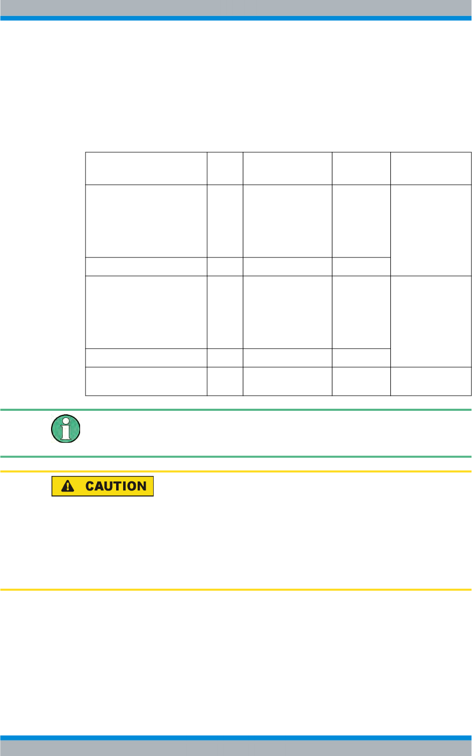
R&S PMU901 Interface Description
R&S® TMU9
119System Manual 2600.5423.02 ─ 01
C R&S PMU901 Interface Description
C.1 X1: Supply Input; Schaltbau M3 connector
Signal
Name/Description
Direc-
tion
Value range Connection
point
Remarks
L Input V AC = 170 V to 264 V
I ≤ 15 A
47 Hz to 63 Hz
cos φ ≥ 0.95 at 230 V
and Pnom
X1.1 Power supply con-
nection for the regu-
lar power supply
N Input 0 V X1.2
LReserve Input V AC = 170 V - 264 V
I ≤ 15 A
47 Hz to 63 Hz
cos φ ≥ 0.95 at 230 V
and Pnom
X1.3 Power supply con-
nection for the
standby power sup-
ply
NReserve Input 0 V X1.5
PE Input 0 V X1.PE Power supply con-
nection
Since the PE connections also need to be fed in separately for separate electrical circuits,
a second protective earth must be ensured via a grounding bolt (40 A test current), since
only one shared PE is fed in on the X1.
Increased leakage current! The instrument must first be connected to the protective
ground. An additional ground wire connection is provided since two power supply circuits
are possible: Automatically pluggable (socket 3587.4188.00, at pin contact 3587.4194.00
on the rack side) for rack installation and as a stud for table operation as well.
Shutoff at all poles for the connecting cables is necessary for two-phase networks (2W
+ PE).
X1: Supply Input; Schaltbau M3 connector

R&S PMU901 Interface Description
R&S® TMU9
120System Manual 2600.5423.02 ─ 01
C.2 X2: RF Output 7/16 - Socket (Rear)
Signal
Name/Description
Direc-
tion
Value range Connection
point
Remarks
RF_OUTPUT Output Pavg,nom=600 W (DVB-
T)
Pavg,max = 650 W/
750 W
Psync,nom = 1400 W
(combined)
470 MHz to 862 MHz
to 50 Ω load, S ≤ 1.4
X2 RF output
C.3 X3: RF Test Socket; SMA Female (Front)
Signal
Name/Description
Direc-
tion
Value range Connection
point
Remarks
RF_MONITOR Output 0.5 V to 1 V / at Psync,nom
-54 dBc to -48 dBc
470 MHz to 862 MHz
X3 RF monitor as an
open test point on the
front panel
C.4 X10: RF Input SMA Female (Rear)
Signal
Name/Description
Direc-
tion
Value range Connection
point
Remarks
RF_IN Input Pavg,nom = ±0 dBm ±
3 dB (DVB-T)
Psync,nom= +3.5 dBm ±
3 dB (ATV combined)
470 MHz to 862 MHz
S11 matching: ≤-16 dB
X10 RF input
X2: RF Output 7/16 - Socket (Rear)
R&S PMU901 Interface Description
R&S® TMU9
121System Manual 2600.5423.02 ─ 01
C.5 X13: Second RF Test Socket for ADE; SMA Female
(Rear)
Signal
Name/Description
Direc-
tion
Value range Connection
point
Remarks
ADE_OUT Output 0.5 V to 1 V / at Psync,nom
-54 dBc to -48 dBc
470 MHz to 862 MHz
X13 RF test point prefera-
bly for connecting the
ADE demodulator
C.6 X22: Fan Connection 1; 4-pin Molex Connector
Signal
Name/Description
Direc-
tion
Value range Connection
point
Remarks
VCC_FAN Output +18 V DC to +28 V DC X22.1
VCC_GND Bidirec-
tional
0 V X22.2
FAN_SPEED Input Open collector X22.3
NC X22.4
The fan connection is located directly on the amplifier board.
C.7 X23: Fan Connection 2; 4-pin Molex Connector
Signal
Name/Description
Direc-
tion
Value range Connection
point
Remarks
VCC_FAN Output +18 V DC to +28 V DC X23.1
VCC_GND Bidirec-
tional
0 V X23.2
FAN_SPEED Input Open collector X23.3
NC X23.4
The fan connection is located directly on the amplifier board.
X13: Second RF Test Socket for ADE; SMA Female (Rear)

R&S PMU901 Interface Description
R&S® TMU9
122System Manual 2600.5423.02 ─ 01
C.8 X11: Amplifier Control Unit; 15-pin D-Sub connector
(rear)
Signal
Name/Description
Direc-
tion
Value range Connection
point
Remarks
SORT1 Bidirec-
tional
0 V to 13 V X11.1 Sort PIN 1, short-cir-
cuit-proof, relative to
CAN_GND,
<1 V: low,
>8 V: high
ADGND Input 0 V ± 1 V X11.9 Analog and digital
ground (in amplifier
isolated from GND in
order to prevent
ground loops)
GND Input 0 V X11.2 Amplifier ground
/AC_FAIL Output Open collector,
I ≤ 10 mA (with ESD
protection),
Ri ≤ 100 Ω,
U≤12 V low: ≤ 2.5 V at
10 mA
X11.10 AC voltage phase
monitor
open: AC OK
low (≤ 2.5 V): No AC,
phase failure, over-
voltage and under-
voltage relative to
CAN_GND
RESET
(Not used in Rohde & Schwarz
generation 9 transmitters)
Input 0 V to 5 V,
≤ 5 mA
Ri approx. 3.3 kΩ
(optocoupler input)
X11.3 high (≥ 1 mA, ≥
3.0 V): Reset, resets
the stored messages
TEMP_FAIL and
REFLECTION rela-
tive to ADGND
AMPL_ON
(Not used in Rohde & Schwarz
generation 9 transmitters)
Input 0 V to 5 V,
≤ 5 mA
Ri approx. 3.3 kΩ
(optocoupler input)
X11.11 high (≥ 1 mA, ≥
3.0 V): Amplifier ON;
relative to ADGND
VREF_PWR
(Not used in Rohde & Schwarz
generation 9 transmitters)
Input 0 V to 5.58 V, relative
to ADGND
RL = 74,4 kΩ
, 4 V = nominal value
X11.4 Reference voltage
for output power, rel-
ative to ADGND
PEAK_AV Input 0 V to 5 V,
≤ 5 mA
Ri approx. 3.3 kΩ
(optocoupler input)
X11.12 Peak/AVG measure-
ment toggling;
high: (≥ 1 mA, ≥
3.0 V): PEAK posi-
tion;
low: AV position; rel-
ative to ADGND
X11: Amplifier Control Unit; 15-pin D-Sub connector (rear)

R&S PMU901 Interface Description
R&S® TMU9
123System Manual 2600.5423.02 ─ 01
Signal
Name/Description
Direc-
tion
Value range Connection
point
Remarks
SHUT_DOWN Input 0 V to 13 V,
≤ 5 mA
Internal pull-up to
CAN_V+ via optocou-
pler
X11.5 Amplifier emergency
shutoff,
open: amplifier inac-
tive (mute) low (≥
2 mA, ≤ 3.0 V): Ampli-
fier in normal mode,
relative to CAN_GND
CAN_GND Input 0 V ± 1 V X11.13 CAN ground (isola-
ted from GND)
CAN_L Bidirec-
tional
CAN_L X11.6 CAN low
CAN_H Bidirec-
tional
CAN_H X11.14 CAN high
CAN_V+ Input + 12 V ± 1 V,
≤ 40 mA (for 100 %
dominant level)
typical: 15 mA
X11.7 CAN transceiver sup-
ply; relative to
CAN_GND (isolated
from GND)
/AC_OK Output Open collector,
I ≤ 10 mA (with ESD
protection via Zener
diode),
Ri ≤ 100 Ω,
U≤12 V low: ≤ 1.5 V at
10 mA
X11.15 AC voltage phase
monitor
low: AC OK
open: No AC, phase
failure, overvoltage
and undervoltage rel-
ative to GND
SORT2 Bidirec-
tional
0 V to 13 V X11.8 Sort PIN 2, relative to
CAN_GND,
<1 V: low,
>8 V: high
X11: Amplifier Control Unit; 15-pin D-Sub connector (rear)

R&S PMU901 Interface Description
R&S® TMU9
124System Manual 2600.5423.02 ─ 01
X11: Amplifier Control Unit; 15-pin D-Sub connector (rear)