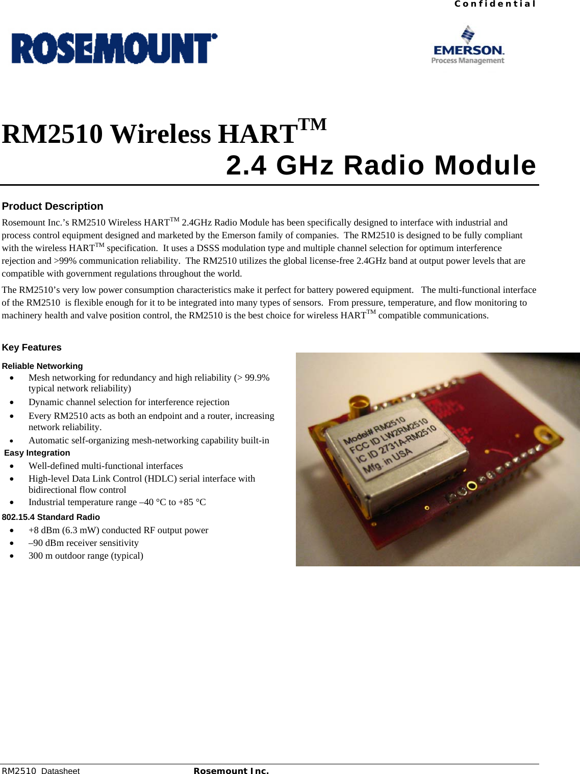
Rosemount RM2510 Wireless HART Industrial Process Management Produc User Manual

Rosemount Inc Wireless HART Industrial Process Management Produc

User manual

 Confidential RM2510  Datasheet Rosemount Inc.  1           RM2510 Wireless HARTTM  2.4 GHz Radio Module  Product Description Rosemount Inc.’s RM2510 Wireless HARTTM 2.4GHz Radio Module has been specifically designed to interface with industrial and process control equipment designed and marketed by the Emerson family of companies.  The RM2510 is designed to be fully compliant with the wireless HARTTM specification.  It uses a DSSS modulation type and multiple channel selection for optimum interference rejection and >99% communication reliability.  The RM2510 utilizes the global license-free 2.4GHz band at output power levels that are compatible with government regulations throughout the world. The RM2510’s very low power consumption characteristics make it perfect for battery powered equipment.   The multi-functional interface of the RM2510  is flexible enough for it to be integrated into many types of sensors.  From pressure, temperature, and flow monitoring to machinery health and valve position control, the RM2510 is the best choice for wireless HARTTM compatible communications.   Key Features Reliable Networking • Mesh networking for redundancy and high reliability (> 99.9% typical network reliability) • Dynamic channel selection for interference rejection • Every RM2510 acts as both an endpoint and a router, increasing network reliability. • Automatic self-organizing mesh-networking capability built-in  Easy Integration • Well-defined multi-functional interfaces • High-level Data Link Control (HDLC) serial interface with bidirectional flow control • Industrial temperature range –40 °C to +85 °C 802.15.4 Standard Radio • +8 dBm (6.3 mW) conducted RF output power  • –90 dBm receiver sensitivity • 300 m outdoor range (typical)
 Confidential  RM2510 Datasheet Rosemount Inc.  2 of 8 Table of Contents  1.0 Absolute Maximum Ratings................................................................................3 2.0 Normal Operating Conditions .............................................................................3 3.0 Electrical Specifications .....................................................................................4 4.0 Radio..................................................................................................................4 4.1 Detailed Radio Specifications ................................................................................ 4 4.2 Antenna Specifications......................................................................................... 5 5.0 Pinout ................................................................................................................5 6.0 Physical Drawing................................................................................................7 7.0 Regulatory and Standards Compliance...............................................................8
 Confidential  RM2510 Datasheet Rosemount Inc.  3 of 8 1.0 Absolute Maximum Ratings The absolute maximum ratings shown below should under no circumstances be violated. Permanent damage to the device may be caused by exceeding one or more of these parameters. Table 1  Absolute Maximum Ratings Parameter  Min  Typ  Max  Units  Comments Supply voltage (VDD to VSS) –0.3  3.6 V  Voltage on any digital I/O pin  –0.3    VDD + 0.3 up to 3.6 V  Input RF level      10  dBm  Input power at antenna connector Storage temperature range  –40    +85  °C   VSWR of antenna      3:1     ESD protection            Antenna pad      ±250  V  HBM  All other pads      ±2  kV  HBM    ±200 V CDM * All voltages are referenced to VSS Caution! ESD sensitive device. Precaution should be used when handling the device in order to prevent permanent damage.  2.0 Normal Operating Conditions Table 2  Normal Operating Conditions Parameter  Min  Typ  Max  Units  Comments Operational supply voltage range (between VDD and VSS)  2.75 3.0  3.3  V Including noise and load regulation Voltage on analog input pins  0    1.8  V   Voltage supply noise      100  mVp-p  50 Hz to 2 MHz Peak current                 85  mA  Flash write 35 ms max         18  mA  TX, 5 ms maximum     6 mA Searching for network, 60 minutes maximum    12 mA  RM2510 boot, see section Error! Reference source not found.. Operating temperature range  –40    +85  °C   Maximum allowed temperature ramp during operation      8  °C/min  –40 °C to +85 °C Operating relative humidity  10    90  % RH  Non-condensing Unless otherwise noted, Table 3  assume VDD is 3.0 V and temperature is 25 °C. Table 3  RM2510 Current Consumption Parameter  Min  Typ  Max  Units  Comments Transmit  18  mA  Receive  6  mA  Sleep  2.5  µA
 Confidential  RM2510 Datasheet Rosemount Inc.  4 of 8 3.0 Electrical Specifications Table 4  Device Load Parameter  Min  Typ  Max  Units  Comments Total capacitance      0.5  µF   Unless otherwise noted, VDD is 3.0 V and temperature is –40 °C to +85 °C. Table 5  Digital I/O Type 1 Digital Signal  Min  Typ  Max  Units  Comments VIL (low-level input voltage)  –0.3    0.6  V   VIH (high-level input voltage)  0.8 x VDD  VDD + 0.3  V   VOL (low-level output voltage)      0.4  V   VOH (high-level output voltage)  2.4      V   Digital current*         Output source (single pin)    3.7    mA  25 °C   Output sink (single pin)    2.0    mA  25 °C Input leakage current    50    nA   * This current level guarantees that the output voltage meets VOH and VOL specifications above.  Table 6  Digital I/O Type 2 Digital Signal  Min  Typ  Max  Units  Comments VIL (low-level input voltage)  –0.3    0.6  V   VIH (high-level input voltage)  0.8 x VDD  VDD + 0.3  V   VOL (low-level output voltage, multi-function I/O configured as output) 0  0.6 V IOL < 0.6 mA, 85 °C VOH low-level output voltage, multi-function I/O configured as output) VDD – 0.6    VDD V IOH > –0.4 mA, 85 °C Digital current*         Output source (single pin, multifunction I/O configured as output)  0.4  mA 25 °C   Output sink (single pin, multifunction I/O configured as output)  0.6  mA 25 °C Input leakage current    50    nA   * This current level guarantees that the output voltage meets VOH and VOL specifications above.  4.0 Radio 4.1 Detailed Radio Specifications Table 7  Radio Specifications Parameter  Min  Typ  Max  Units  Comments Operating frequency  2.4000  2.4835 GHz  Number of channels    15       Channel separation    5    MHz   Occupied channel bandwidth    2.7    MHz  At –20 dBc
 Confidential  RM2510 Datasheet Rosemount Inc.  5 of 8 Parameter  Min  Typ  Max  Units  Comments Frequency Accuracy  -50    +50  kHz   Modulation      IEEE 802.15.4 DSSS Raw data rate    250    kbps   Receiver operating maximum input level   0   dBm  Receiver sensitivity   –92.5   dBm At 50% PER, VDD = 3 V,  25 °C   –90  dBm At 1% PER, VDD = 3 V,  25 °C, (inferred from 50% PER measurement) Output power, conducted      +8  dBm  VDD = 3 V, 25 °C Range*        Indoor    100    m  Outdoor    300    m 25 °C, 50% RH, 1 meter above ground, +2 dBi  omni-directional antenna *  Actual RF range performance is subject to a number of installation-specific variables including, but not restricted to ambient temperature, relative humidity, presence of active interference sources, line-of-sight obstacles, near-presence of objects (for example, trees, walls, signage, and so on) that may induce multipath fading. As a result, actual performance varies for each instance. 4.2 Antenna Specifications The antenna must meet specifications in Table 8. Table 8  Antenna Specifications Parameter  Value Frequency range  2.4–2.4835 GHz Impedance  50 Ω Maximum VSWR  3:1 Antenna Connector  MMCX When the RM2510 is placed inside an enclosure, the antenna should be mounted such that the radiating portion of the antenna protrudes from the enclosure, and connected using a coaxial cable. For optimum performance, allow the antenna to be positioned vertically when installed.  5.0 Pinout  The following is the pinout for the RM2510 module. Table 9  Pinout Assignments for the RM2510 Pin Number  Pin Description  I/O (relative to radio) 1-1 Circuit Common/Ground  Input 1-2  Power Supply (2.75 V to 3.3 V)  Input 1-3  Keying Pin (no function)  N/A 1-4  Data Transmit (Sensor Board to Radio)  Input 1-5  Data Receive (Radio to Sensor Board)  Output 1-6 Diagnostics LED  Output 1-7  Radio Ready-to-Send (also DIM wake-up)  Output 1-8 Radio Clear-to-Send  Output 1-9  Sensor Board Clear-to-Send  Input 1-10  Radio Time Packet  Input 1-11  Radio Baud Rate Input  Input
 Confidential  RM2510 Datasheet Rosemount Inc.  6 of 8 2-1  Radio Reset Line  Input 2-2  SPI Chip Select  Input 2-3  Keying Pin (no function)  N/A 2-4  SPI Bus (MISO)  Output 2-5  SPI Bus (MOSI)  Input 2-6  SPI Bus (Clock)  Input 2-7 JTAG (TCK)  Input 2-8 JTAG (TDO)  Output 2-9 JTAG (TDI)  Input 2-10 JTAG (TMS)  Input 2-11 Flash Enable  Input
 Confidential  RM2510 Datasheet Rosemount Inc.  7 of 8  6.0 Physical Drawing                      Figure 1  RM2510 Mechanical Drawing
 Confidential  RM2510 Datasheet Rosemount Inc.  8 of 8 7.0 Regulatory and Standards Compliance The RM2510 has achieved modular radio certification on a reference design for the United States, Canada and the Europe.  The reference design has been certified for Part 15.247 (Intentional Radiator) of the FCC rules an regulations, Industry Canada RSS-210, ETSI EN 300 328 and ETSI EN 301-489-17. This device complies with part 15 of the FCC Rules. Operation is subject to the following two conditions: (1) This device may not cause harmful interference, and (2) this device must accept any interference received, including interference that may cause undesired operation. Note: This equipment has been tested and found to comply with the limits for a Class A digital device, pursuant to part 15 of the FCC Rules.  These limits are designed to provide reasonable protection against harmful interference when the equipment is operated in a commercial environment.  This equipment generates, uses, and can radiate radio frequency energy and, if not installed and used in accordance with the instruction manual, may cause harmful interference to radio communications.  Operation of this equipment in a residential area is likely to cause harmful interference in which case the user will be required to correct the interference at his own expense. The RM2510 complies with Part 15.247 modular (Intentional Radiator) FCC rules and regulations. Changes or modifications not expressly approved by Rosemount Inc. could void the user's authority to operate the equipment. 7.1 FCC Testing In order to fulfill FCC certification requirements, products incorporating the RM2510 must comply with the following: 1. An external label must be provided on the outside of the final product enclosure specifying the FCC identifier as described in 7.3 below. 2. The antenna must be electrically identical to the FCC-approved antenna specifications for the RM2510 as described in 7.2 with the exception that the gain may be lower than specified in Table 14. 3. The device integrating the RM2510 may not cause harmful interference, and must accept any interference received, including interference that may cause undesired operation. 4. An unintentional radiator scan must be performed on the device integrating the RM2510, per FCC rules and regulations, CFR Title 47, Part 15, Subpart B. See FCC rules for specifics on requirements for declaration of conformity. 7.2 FCC-approved Antenna The FCC-approved antenna specifications for the RM2510 is an antenna with a Maximum gain of +2dBi, vertical polarization, and frequency of 2.4 to 2.485GHz. 7.3 Final FCC Labeling Requirements The outside of the final product enclosure must have a label with the following (or similar) text specifying the FCC identifier. The FCC ID and certification code must be in Latin letters and Arabic numbers and visible without magnification. Contains transmitter module FCC ID: LW2RM2510 Or Contains FCC ID: LW2RM2510 7.4 IC Testing The RM2510 is certified for modular Industry Canada (IC) RSS-210 approval. The OEM is responsible for its product to comply with IC ICES-003 and FCC Part 15, Sub. B - Unintentional Radiators. The requirements of ICES-003 are equivalent to FCC Part 15 Sub. B and Industry Canada accepts FCC test reports or CISPR 22 test reports for compliance with ICES-003. 7.5 Final IC Labeling Requirements The Original Equipment Manufacturer (OEM) must ensure that IC labeling requirements are met. The outside of the final product enclosure must have a label with the following (or similar) text specifying the IC identifier. The IC ID and certification code must be in Latin letters and Arabic numbers and visible without magnification Contains IC: 2731A-RM2510   Rosemount Inc. 8200 Market Boulevard Chanhassen, MN  55317 USA

Navigation menu