SAGEMCOM BROANDS HILONC-3GPS Qual-Band GSM/GPRS/EDGE Voice and Data Module User Manual rev1
SAGEMCOM SAS Qual-Band GSM/GPRS/EDGE Voice and Data Module rev1
UserManual.wiki
>
SAGEMCOM BROANDS
>
HILONC 3GPS User Manual
User manual rev1
Navigation menu
Upload a User Manual
Namespaces
Wiki Guide
HTML
PDF
Info
Views
User Manual
Discussion / Help
Navigation
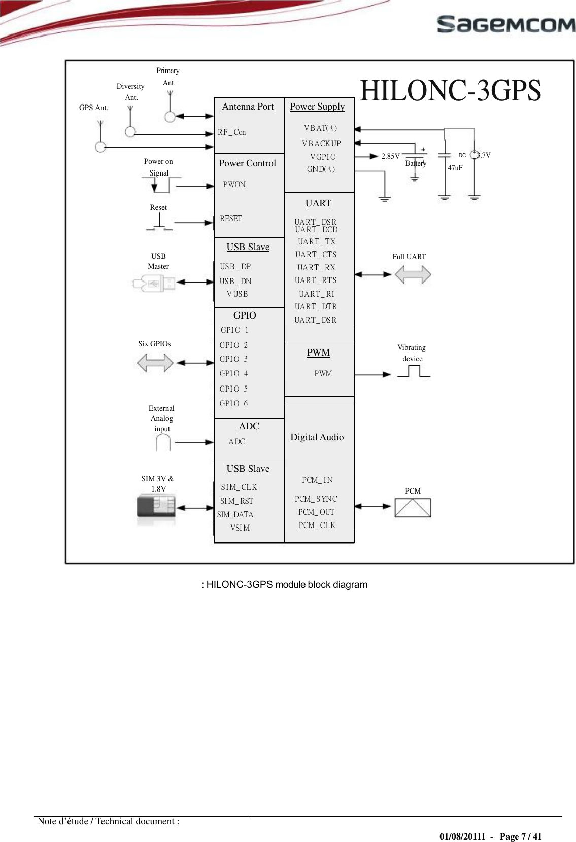
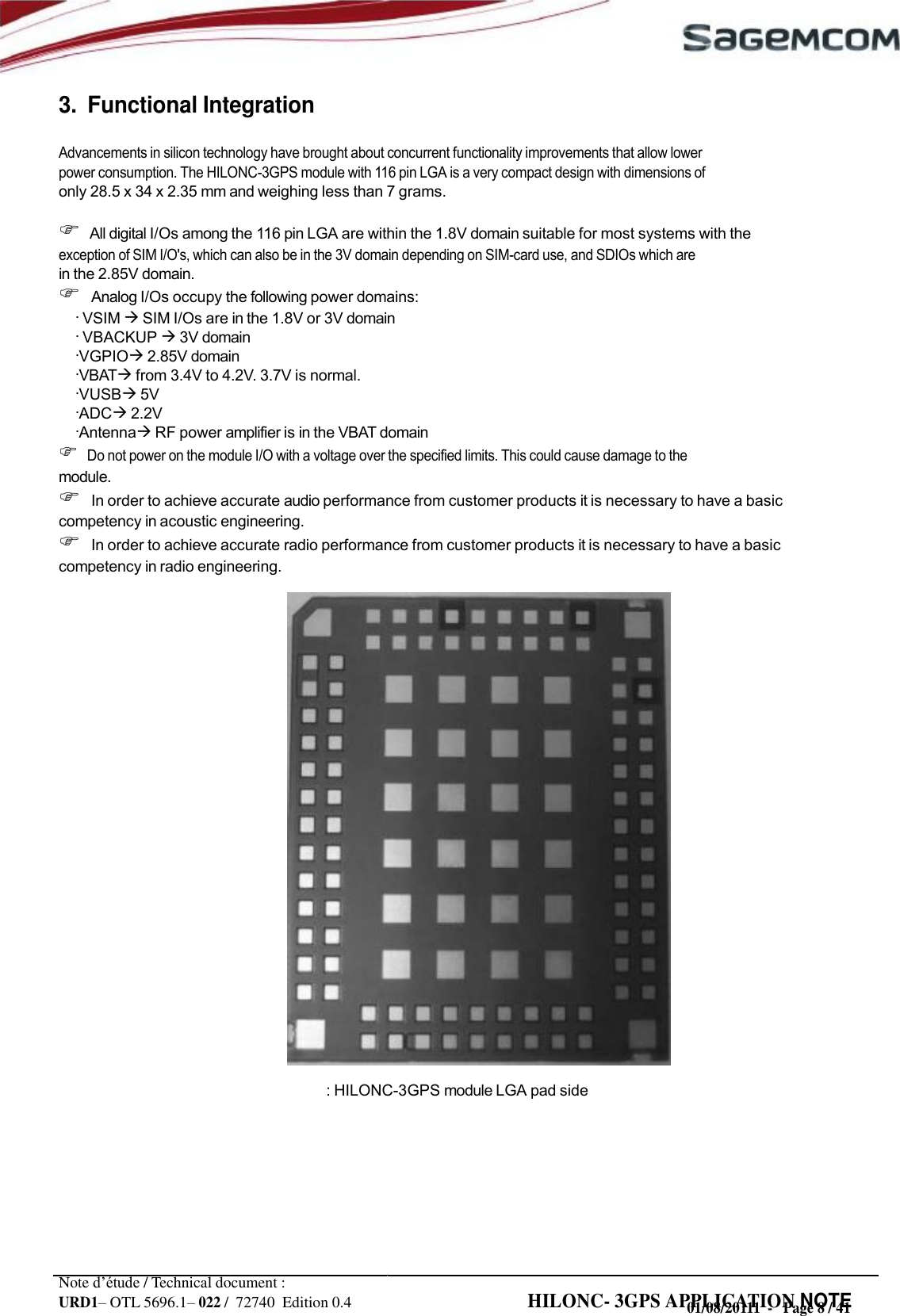
![URD1– OTL 5696.1– 022 / 72740 Edition 0.4 HILONC- 3GPS APPLICATION NOTE 1. OVERVIEW 1.1. Document Objectives The aim of this document is to provide examples of hardware solutions for development of products based around the Sagemcom HiLo NC-3GPS Module. Most of these solutions are not mandatory. Use them as suggestions of what should be done to achieve a working product and what should be avoided according to our own experiences. This document gives suggestions on how to integrate the HiLo NC-3GPS module into devices for automotive applications, AMM (Automatic Metering Management), tracking systems; including connection with external devices, layout advices, external components (decoupling etc. 1.2. Reference Documents [1] URD1 OTL 5696 3 001 72497- HILONC-3GPS technical specifications [2] URD1 OTL 5696.1 006 72370- AT Command Set for SAGEM HILONC-3GPS Modules 1.3. Document Modifications The information presented in this document should be accurate and reliable. However Sagemcom assumes no responsibility for its use, nor any infringement of patents or other third party rights which may result from its use. This document is subject to change without notice. Changes or modifications not expressly approved by the party responsible for compliance could void the authority to operate the equipment. 1.4. Conventions SIGNAL NAMES: All signal names written on the pins of the HILONC-3GPS module are in italics. Special attention must be paid to the information on them. 2. Block Diagram Note d’étude / Technical document : 01/08/20111 - Page 6 / 41](https://usermanual.wiki/SAGEMCOM-BROANDS/HILONC-3GPS/User-Guide-1685824-Page-6.png)
![URD1– OTL 5696.1– 022 / 72740 Edition 0.4 HILONC- 3GPS APPLICATION NOTE - Global System for Mobile communications (GSM); Harmonized standard for mobile stations in the GSM 900 and DCS 1800 bands covering essential requirements under article 3.2 of the R&TTE directive (1999/5/EC) EN 301 489-1 V1.8.1: 2008 Electromagnetic compatibility and Radio Spectrum Matters (ERM); ElectroMagnetic Compatibility (EMC) standard for radio equipment and services; Part 1: Common technical requirements EN 301 489-7 V1.3.1: 2005 ElectroMagnetic compatibility and Radio spectrum Matters (ERM); ElectroMagnetic Compatibility (EMC) standard for radio equipment ad services; Part 7: Specific conditions for mobile and portable radio and ancillary equipment of digital cellular radio telecommunications systems (GSM and DCS) EN 301 489-24 V1.5.1: 2010 Electromagnetic compatibility and Radio Spectrum Matters (ERM); ElectroMagnetic Compatibility (EMC) standard for radio equipment and services; Part 24: Specific conditions for IMT-2000 CDMA Direct Spread (UTRA) for Mobile and portable (UE) radio and ancillary equipment EN 301 489-3 V1.4.10682 Note d’étude / Technical document : 01/08/20111 - Page 36 / 41 [Czech] [Jméno výrobce] tímto tento [typ zařízení] je ve se základními a ustanoveními 1999/5/ES. Dansk [Danish] Undertegnede [fabrikantens navn] erklærer herved, at følgende udstyr [udstyrets typebetegnelse] overholder de væsentlige krav og øvrige relevante krav i direktiv 1999/5/EF. Deutsch [German] Hiermit erklärt [Name des Herstellers], dass sich das Gerät [Gerätetyp] in Übereinstimmung mit den grundlegenden Anforderungen und den übrigen einschlägigen Bestimmungen der Richtlinie 1999/5/EG befindet. Eesti [Estonian] Käesolevaga kinnitab [tootja nimi = name of manufacturer] seadme [seadme tüüp = type of equipment] vastavust direktiivi 1999/5/EÜ põhinõuetele ja nimetatud direktiivist tulenevatele teistele asjakohastele sätetele. English Hereby, [name of manufacturer], declares that this [type of equipment] is in compliance with the essential requirements and other relevant provisions of Directive 1999/5/EC. Español [Spanish] Por medio de la presente [nombre del fabricante] declara que el [clase de equipo] cumple con los requisitos esenciales y cualesquiera otras disposiciones aplicables o exigibles de la Directiva 1999/5/CE. [Greek] [name of manufacturer] [type of equipment] Français [French] Par la présente [nom du fabricant] déclare que l'appareil [type d'appareil] est conforme aux exigences essentielles et aux autres dispositions pertinentes de la directive 1999/5/CE. Italiano [Italian] Con la presente [nome del costruttore] dichiara che questo [tipo di apparecchio] è conforme ai requisiti essenziali ed alle altre disposizioni pertinenti stabilite dalla direttiva 1999/5/CE. Latviski [Latvian] Ar [name of manufacturer / izgatavotāja nosaukums] ka [type of equipment / iekārtas tips] atbilst 1999/5/EK un citiem ar to noteikumiem. [Lithuanian] [manufacturer name] deklaruoja, kad s [equipment type] atitinka esminius reikalavimus ir kitas 1999/5/EB Direktyvos nuostatas. Nederlands [Dutch] Hierbij verklaart [naam van de fabrikant] dat het toestel [type van toestel] in overeenstemming is met de essentiële eisen en de andere relevante bepalingen van richtlijn 1999/5/EG. Malti [Maltese] Hawnhekk, [isem tal-manifattur], jiddikjara li dan [il-mudel tal-prodott] jikkonforma mal- essenzjali u ma provvedimenti relevanti li hemm fid-Dirrettiva 1999/5/EC. Magyar [Hungarian] Alulírott, [gyártó neve] nyilatkozom, hogy a [... típus] megfelel a vonatkozó alapvetõ követelményeknek és az 1999/5/EC irányelv egyéb elõírásainak.](https://usermanual.wiki/SAGEMCOM-BROANDS/HILONC-3GPS/User-Guide-1685824-Page-36.png)
![URD1– OTL 5696.1– 022 / 72740 Edition 0.4 HILONC- 3GPS APPLICATION NOTE Federal Communication Commission Interference Statement This device complies with Part 15 of the FCC Rules. Operation is subject to the following two conditions: (1) This device may not cause harmful interference, and (2) this device must accept any interference received, including interference that may cause undesired operation. This equipment has been tested and found to comply with the limits for a Class B digital device, pursuant to Part 15 of the FCC Rules. These limits are designed to provide reasonable protection against harmful interference in a residential installation. This equipment generates, uses and can radiate radio frequency energy and, if not installed and used in accordance with the instructions, may cause harmful interference to radio communications. However, there is no guarantee that interference will not occur in a particular installation. If this equipment does cause harmful interference to radio or television reception, which can be determined by turning the equipment off and on, the user is encouraged to try to correct the interference by one of the following measures: - Reorient or relocate the receiving antenna. - Increase the separation between the equipment and receiver. - Connect the equipment into an outlet on a circuit different from that to which the receiver is connected. -Consult the dealer or an experienced radio/TV technician for help. FCC Caution: Any changes or modifications not expressly approved by the party responsible for compliance could void the user's authority to operate this equipment. This transmitter must not be co-located or operating in conjunction with any other antenna or transmitter. This device complies with FCC radiation exposure limits set forth for an uncontrolled environment. In order to avoid the possibility of exceeding the FCC radio frequency exposure limits, human proximity to the antenna shall not be less than 20cm (8 inches) during normal operation. Note d’étude / Technical document : 01/08/20111 - Page 37 / 41Polski [Polish] Niniejszym [nazwa producenta] [nazwa wyrobu] jest zgodny z zasadniczymi wymogami oraz stosownymi postanowieniami Dyrektywy 1999/5/EC. Português [Portuguese] [Nome do fabricante] declara que este [tipo de equipamento] está conforme com os requisitos essenciais e outras disposições da Directiva 1999/5/CE. Slovensko [Slovenian] [Ime proizvajalca] izjavlja, da je ta [tip opreme] v skladu z bistvenimi zahtevami in ostalimi relevantnimi i direktive 1999/5/ES. Slovensky [Slovak] [Meno výrobcu] týmto vyhlasuje, [typ zariadenia] základné a ustanovenia Smernice 1999/5/ES. Suomi [Finnish] [Valmistaja = manufacturer] vakuuttaa täten että [type of equipment = laitteen tyyppimerkintä] tyyppinen laite on direktiivin 1999/5/EY oleellisten vaatimusten ja sitä koskevien direktiivin muiden ehtojen mukainen. Svenska [Swedish] Härmed intygar [företag] att denna [utrustningstyp] står I överensstämmelse med de väsentliga egenskapskrav och övriga relevanta bestämmelser som framgår av direktiv 1999/5/EG.](https://usermanual.wiki/SAGEMCOM-BROANDS/HILONC-3GPS/User-Guide-1685824-Page-37.png)
![URD1– OTL 5696.1– 022 / 72740 Edition 0.4 HILONC- 3GPS APPLICATION NOTE End Product Labeling This transmitter module is authorized only for use in device where the antenna may be installed such that 20 cm may be maintained between the antenna and users. The final end product must be labeled in a visible area with the following: FCC ID: VW3HILONC-3GPS Contains IC: 9140A-HILONC-3GPS The grantee's FCC ID/IC ID can be used only when all FCC/Canada compliance requirements are met. Plaque signalétique du produit final Ce module émetteur est autorisé uniquement pour une utilisation dans un dispositif où l'antenne peut être installée de telle sorte qu'une distance de 20cm peut être maintenue entre l'antenne et les utilisateurs. Le produit final doit être étiqueté dans un endroit visible avec l'inscription suivante: "Contient des IC: 9140A- HILONC-3GPS". Manual Information To the End User The OEM integrator has to be aware not to provide information to the end user regarding how to install or remove this RF module in the manual of the end product which integrates this module. The end user manual shall include all required regulatory information/warning as show in this manual. Manuel d'information à l'utilisateur final L'intégrateur OEM doit être conscient de ne pas fournir des informations à l'utilisateur final quant à la façon d'installer ou de supprimer ce module RF dans le manuel de l'utilisateur du produit final qui intègre ce module. Le manuel de l'utilisateur final doit inclure toutes les informations réglementaires requises et avertissements comme indiqué dans ce manuel. This device has been designed to operate with a dipole antenna have a maximum gain of [0.6] dB. Antenna having a higher gain is strictly prohibited per regulations of Industry Canada. The required antenna impedance is 50 ohms. Under Industry Canada regulations, this radio transmitter may only operate using an antenna of a type and maximum (or lesser) gain approved for the transmitter by Industry Canada. To reduce potential radio interference to other users, the antenna type and its gain should be so chosen that the equivalent isotropically radiated power (e.i.r.p.) is not more than that necessary for successful communication. This radio transmitter (IC: 9140A-HILONC-3GPS / Model: HiLoNC-3GPS ) has been approved by Industry Canada to operate with the antenna type, maximum permissible gain and required antenna impedance for each antenna type indicated. Antenna types not included in this manual, having a gain greater than the maximum gain indicated for that type, are strictly prohibited for use with this device. Ce dispositif a été conçu pour fonctionner avec une antenne ayant un gain maximal de dipole antenne avec dB [0.6]. Une antenne à gain plus élevé est strictement interdite par les règlements d'Industrie Canada. L'impédance d'antenne requise est de 50 ohms. Note d’étude / Technical document : 01/08/20111 - Page 39 / 41](https://usermanual.wiki/SAGEMCOM-BROANDS/HILONC-3GPS/User-Guide-1685824-Page-39.png)