SAGEMCOM BROANDS HILONC-3GPS Qual-Band GSM/GPRS/EDGE Voice and Data Module User Manual rev1
SAGEMCOM SAS Qual-Band GSM/GPRS/EDGE Voice and Data Module rev1
User manual rev1
URD1
– OTL 5696.1–
022
/ 72740 Edition 0.4
HILONC-
3GPS
APPLICATION
NOTE
01/08/
2011 - page 1/41
Direction
des
Recherches
et
des
Développements
Etablissement de RUEIL-MALMAISON
RUEIL-MALMAISON
R&D
Center
NOTE
D'ETUDE
/
TECHNICAL
DOCUMENT
ETUDE
/
PROJECT
NOM
DE
L’ETUDE
HILONC-3GPS
TITRE
/
TITLE
:
HILONC-
3GPS
APPLICATION
NOTE
RESUME
/
SUMMARY
This document is the application notes of the HILONC-3GPS module.
Mots clés /
Keywords
:
HiLoNC-3GPS,
application
Note
DIFFUSION
INTERNE
/
INTERNAL
DISTRIBUTION
REDACTEUR(S) / AUTHOR (S) + F.FREULON, F.GOUERE .
DIFFUSION EXTERNE sous convention de confidentialité :
EXTERNAL DISTRIBUTION with confidentiality agreement :
………….
Enregistrement
relatif
à
la
qualité
(ERQ)
/
Quality
record
A
déposer
en
enveloppe
soleau
/
Put
in
a
soleau
envelope
Note d’étude / Technical document :
Edition
Approbations
/
Approvals
N°
#
0.4
Nom
Name
Rédacteur(s)
Author(s)
CC Hsieh
Chef
de
projet
Project
design
manager
CC Hsieh
Responsable
d’entité
/
Product
design
manager
CW Sheu
Chef
Unité
R&D
unit
manager
P. NOM
Assurance
Qualité
/
R&D
quality
assurance
Harry Lin
Date
Signature
01/08/2011
Aaron Wang
19/09/2011
CC Hsieh
19/09/2011
Ruth Chu
28/07/2011
21/09/2011
Harry Lin
REFERENCE
URD1
–
OTL
5696.1–022/
72740
Code
C
TA1

URD1
– OTL 5696.1–
022
/ 72740 Edition 0.4
HILONC-
3GPS
APPLICATION
NOTE
NOTE
D'ETUDE
/
TECHNICAL
DOCUMENT
FICHE
RECAPITULATIVE
/
SUMMARY
SHEET
Note d’étude / Technical document :
01/08/20111
-
Page
2
/
41
Ed
Date
Date
Référence
Reference
Rédacteur(s)
Author(s)
Relecteur(s)
Reviser(s)
Pages
modifiées
/
Changed
pages
Observations
Comments
0.1
23/09/2011
URD1 OTL 5696.1
022 72740 ed 0.1 -
HiLoNC-3GPS
Application Note
SAGEMCOM
SAGEMCOM.
All
First Draft release
0.2
17/10/2011
URD1 OTL 5696.1
022 72740 ed 0.2 -
HiLoNC-3GPS
Application Note
SAGEMCOM
SAGEMCOM
Modification in the
Sim schematics, PU
on sim data
removed
0.3
09/11/2011
URD1 OTL 5696.1
022 72740 ed 0.3 -
HiLoNC-3GPS
Application Note
SAGEMCOM
SAGEMCOM
MSL chapter added
0.4
03/12/2011
URD1 OTL 5696.1
022 72740 ed 0.4 -
HiLoNC-3GPS
Application Note
SAGEMCOM
SAGEMCOM
RTC and mechanical
chapters improved
1

URD1
– OTL 5696.1–
022
/ 72740 Edition 0.4
HILONC-
3GPS
APPLICATION
NOTE
SOMMAIRE
/
CONTENTS
1.
OVERVIEW...................................................................................................................................................................
6
1.1.
Document
Objectives
..........................................................................................................................................
6
1.2.
Reference
Documents
.........................................................................................................................................
6
1.3.
Document
Modifications
......................................................................................................................................
6
1.4.
Conventions
..........................................................................................................................................................
6
2.
Block
Diagram...............................................................................................................................................................
6
3.
Functional
Integration....................................................................................................................................................
8
3.1.
How
to
connect
a
SIM
card
................................................................................................................................
9
3.2.
Audio
Connection
...............................................................................................................................................
11
3.2.1.
PCM
Digital
Audio
......................................................................................................................................
11
3.3.
PWM
....................................................................................................................................................................
14
3.3.1.
PWM
for
Buzzer
connection
.....................................................................................................................
14
3.3.2.
Network
LED
...............................................................................................................................................
15
3.4.
Power
Requirements
.........................................................................................................................................
15
3.5.
UART
...................................................................................................................................................................
16
3.5.1.
Complete
V24
Connection
of
HILONC-3GPS
to
host
..........................................................................
16
3.5.2.
Complete
V24
Interface
with
PC
..............................................................................................................
17
3.5.3.
Partial
V24
(RX-TX-RTS-CTS)
Connection
of
HILONC-3GPS
to
host
..............................................
18
3.5.4.
Partial
V24
(RX-TX)
Connection
of
HILONC-3GPS
to
host
................................................................
19
3.6.
GPIO
....................................................................................................................................................................
19
3.7.
ADC
......................................................................................................................................................................
20
3.8.
Backup
Battery
...................................................................................................................................................
20
3.8.1.
Backup
Battery
Function
Features
..........................................................................................................
20
3.8.2.
Internal
HILONC-3GPS
Charging
Function
...........................................................................................
20
3.8.3.
Backup
Battery
Technology
......................................................................................................................
21
3.9.
USB
......................................................................................................................................................................
21
4.
Power
Management
......................................................................................................................................................
21
4.1.
Power
Modes
......................................................................................................................................................
21
4.2.
Module
Power
up
...............................................................................................................................................
22
4.2.1.
PWON
Power
up
........................................................................................................................................
22
4.2.2.
IO
DC
Presence
before
Power
on
...........................................................................................................
22
4.3.
Power
on
and
Sleep
Diagrams
........................................................................................................................
22
4.4.
Module
Power
off
...............................................................................................................................................
22
4.4.1.
UART
Interface
...........................................................................................................................................
23
4.4.2.
USB
Interface
.............................................................................................................................................
23
4.5.
Sleep
Mode
.........................................................................................................................................................
23
5.
ESD & EMC Recommendations ..................................................................................................................................
24
5.1.
HILONC-3GPS
Handling
..................................................................................................................................
24
5.2.
ESD
Recommendations
....................................................................................................................................
24
5.2.1.
Avoiding
ESD
..............................................................................................................................................
24
5.3.
EMC
recommendations
.....................................................................................................................................
24
6.
Radio
Integration
..........................................................................................................................................................
24
6.1.
Antenna
Connection
..........................................................................................................................................
25
6.1.1.
Antenna
Pad
...............................................................................................................................................
25
6.1.2.
Antenna
Recommendations
.....................................................................................................................
26
6.2.
Ground
Link
Area
...............................................................................................................................................
27
6.3.
Layout
..................................................................................................................................................................
27
6.4.
Mechanical
Recommendations
........................................................................................................................
27
6.5.
Other
Recommendation
-
production/design
test
..........................................................................................
27
7.
Audio
Integration..........................................................................................................................................................
27
7.1.
Mechanical
integration
and
acoustics
.............................................................................................................
27
7.2.
Electronics
and
layout
.......................................................................................................................................
28
Note d’étude / Technical document :
01/08/20111
-
Page
3
/
41

URD1
– OTL 5696.1–
022
/ 72740 Edition 0.4
HILONC-
3GPS
APPLICATION
NOTE
8.
Recommendations
on
customer
board
layout
...............................................................................................................
28
8.1.
General
recommendations
on
layout
..............................................................................................................
28
8.1.1.
Ground
.........................................................................................................................................................
28
8.1.2.
Ground
layout
guidelines
..........................................................................................................................
28
8.1.3.
Digital
ground
..............................................................................................................................................
29
8.1.4.
Analog/RF
ground
......................................................................................................................................
29
8.1.5.
Power
supply
..............................................................................................................................................
29
8.1.6.
Clocks
..........................................................................................................................................................
29
8.1.7.
Data
bus
and
other
signals
.......................................................................................................................
29
8.1.8.
Radio
............................................................................................................................................................
29
8.1.9.
Shielding
......................................................................................................................................................
29
8.2.
Example
of
a
customer
board
layout
...............................................................................................................
30
9.
Moisture sensitivity level precautions ..........................................................................................................................
30
10
CUSTOMER
PROCESS
................................................................................................................................................
31
10.1
PACKAGE
.............................................................................................................................................................
31
10.2
Stencil
....................................................................................................................................................................
32
10.2.1
Fotprint
...........................................................................................................................................................
32
10.2.2
Recommended
Stencil
design
....................................................................................................................
33
10.3
Solder
Paste
.........................................................................................................................................................
33
10.4
Profile
for
Reflow
soldering
.................................................................................................................................
33
10.5
SMT
Machine
........................................................................................................................................................
34
10.5.1
Nozzles
...........................................................................................................................................................
34
10.5.2
Fiducials
.........................................................................................................................................................
34
10.6
Underfill
.................................................................................................................................................................
34
10.7
Second
reflow
soldering
.......................................................................................................................................
34
10.8
Hand
soldering
.....................................................................................................................................................
35
10.9
UnsolderING
.........................................................................................................................................................
35
11.
Labelling
..................................................................................................................................................................
35
12
CE/FCC/IC
warning
statement
.............................................................................................................................
35
Note d’étude / Technical document :
01/08/20111
-
Page
4
/
41

URD1
– OTL 5696.1–
022
/ 72740 Edition 0.4
HILONC-
3GPS
APPLICATION
NOTE
Note d’étude / Technical document :
01/08/20111
-
Page
5
/
41

URD1
– OTL 5696.1–
022
/ 72740 Edition 0.4
HILONC-
3GPS
APPLICATION
NOTE
1.
OVERVIEW
1.1.
Document
Objectives
The aim of this document is to provide examples of hardware solutions for development of products based
around the Sagemcom HiLo NC-3GPS Module. Most of these solutions are not mandatory. Use them as
suggestions
of
what
should
be
done
to
achieve
a
working
product
and
what
should
be
avoided
according
to
our
own experiences.
This
document
gives
suggestions
on
how
to
integrate
the
HiLo
NC-3GPS
module
into
devices
for
automotive
applications,
AMM
(Automatic
Metering
Management),
tracking
systems;
including
connection
with
external
devices, layout advices, external components (decoupling etc.
1.2.
Reference
Documents
[1] URD1 OTL 5696 3 001 72497- HILONC-3GPS technical specifications
[2] URD1 OTL 5696.1 006 72370- AT Command Set for SAGEM HILONC-3GPS Modules
1.3.
Document
Modifications
The
information
presented
in
this
document
should
be
accurate
and
reliable.
However
Sagemcom
assumes
no
responsibility
for
its
use,
nor
any
infringement
of
patents
or
other
third
party
rights
which
may
result
from
its
use.
This document is subject to change without notice.
Changes
or
modifications
not
expressly
approved
by
the
party
responsible
for
compliance
could
void
the
authority to operate the equipment.
1.4.
Conventions
SIGNAL NAMES: All signal names written on the pins of the HILONC-3GPS module are in italics.
Special attention must be paid to the information on them.
2.
Block
Diagram
Note d’étude / Technical document :
01/08/20111
-
Page
6
/
41
URD1
– OTL 5696.1–
022
/ 72740 Edition 0.4
HILONC-
3GPS
APPLICATION
NOTE
Primary
GPS
Ant.
Diversity
Ant.
Ant.
HILONC-3GPS
Power
on
Signal
2.85V
Battery
DC
3.7V
47uF
Reset
USB
Master
Six
GPIOs
Full
UART
Vibrating
device
External
Analog
input
SIM
3V
&
1.8V
PCM
:
HILONC-3GPS
module
block
diagram
Note
d’étude
/
Technical
document
:
01/08/20111
-
Page
7
/
41
Antenna Port
R F _ Con
Power Supply
V B AT( 4 )
V B A CK UP
V GP I O
GN D( 4 )
Power Control
P WON
RESET
UART
UA R T _ DS R
UA R T _ DCD
UA R T _ T X
UA R T _ CT S
UA R T _ R X
UA R T _ R T S
UA R T _ R I
UA R T _ DT R
UA R T _ DS R
USB Slave
US B _ DP
US B _ DN
V US B
GPIO
GP I O 1
GP I O 2
GP I O 3
GP I O 4
GP I O 5
GP I O 6
PWM
P WM
Digital Audio
P CM_ I N
P CM_ S YN C
P CM_ OUT
P CM_ CL K
ADC
A DC
USB Slave
S I M_ CL K
SI M_ RST
S I M _ DA T A
VSI M
URD1
– OTL 5696.1–
022
/ 72740 Edition 0.4
HILONC-
3GPS
APPLICATION
NOTE
3.
Functional
Integration
Advancements
in
silicon
technology
have
brought
about
concurrent
functionality
improvements
that
allow
lower
power
consumption.
The
HILONC-3GPS
module
with
116
pin
LGA
is
a
very
compact
design
with
dimensions
of
only 28.5 x 34 x 2.35 mm and weighing less than 7 grams.
All digital I/Os among the 116 pin LGA are within the 1.8V domain suitable for most systems with the
exception
of
SIM
I/O's,
which
can
also
be
in
the
3V
domain
depending
on
SIM-card
use,
and
SDIOs
which
are
in the 2.85V domain.
Analog I/Os occupy the following power domains:
· VSIM SIM I/Os are in the 1.8V or 3V domain
· VBACKUP 3V domain
·VGPIO 2.85V domain
·VBAT from 3.4V to 4.2V. 3.7V is normal.
·VUSB 5V
·ADC 2.2V
·Antenna RF power amplifier is in the VBAT domain
Do
not
power
on
the
module
I/O
with
a
voltage
over
the
specified
limits.
This
could
cause
damage
to
the
module.
In order to achieve accurate audio performance from customer products it is necessary to have a basic
competency in acoustic engineering.
In order to achieve accurate radio performance from customer products it is necessary to have a basic
competency in radio engineering.
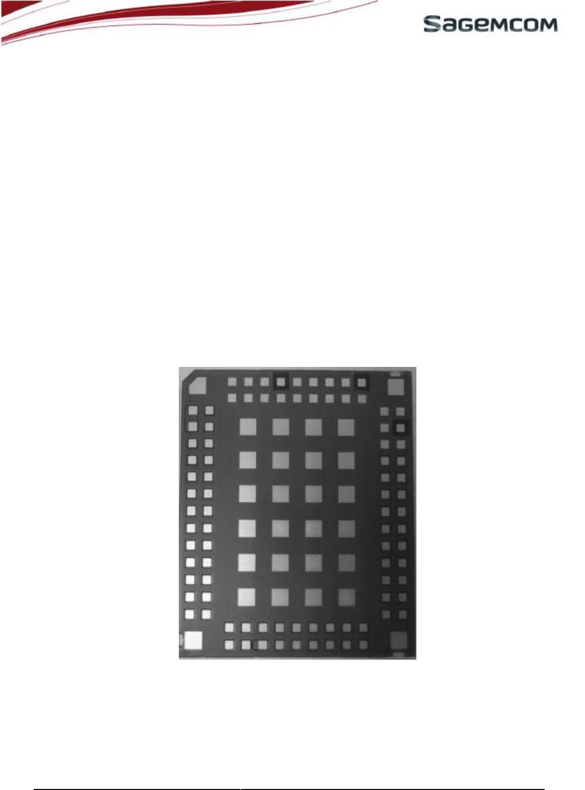
: HILONC-3GPS module LGA pad side
Note d’étude / Technical document :
01/08/20111
-
Page
8
/
41
URD1
– OTL 5696.1–
022
/ 72740 Edition 0.4
HILONC-
3GPS
APPLICATION
NOTE
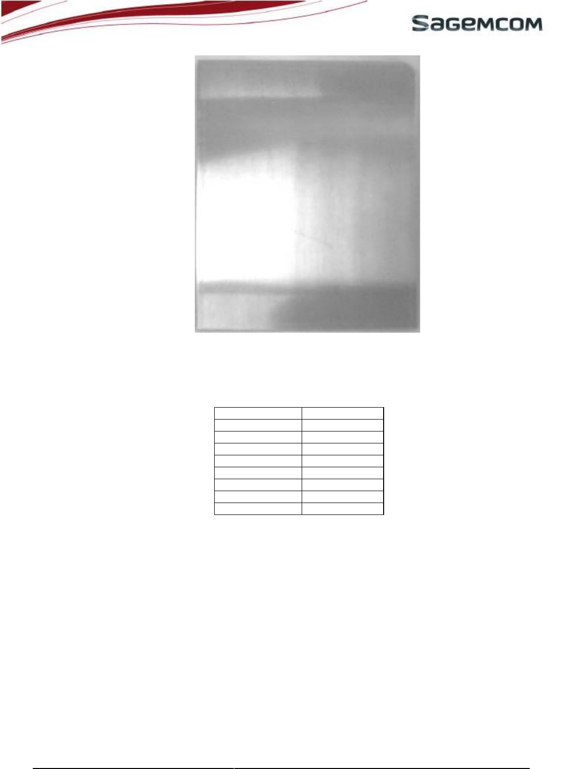
: HILONC-3GPS module top side
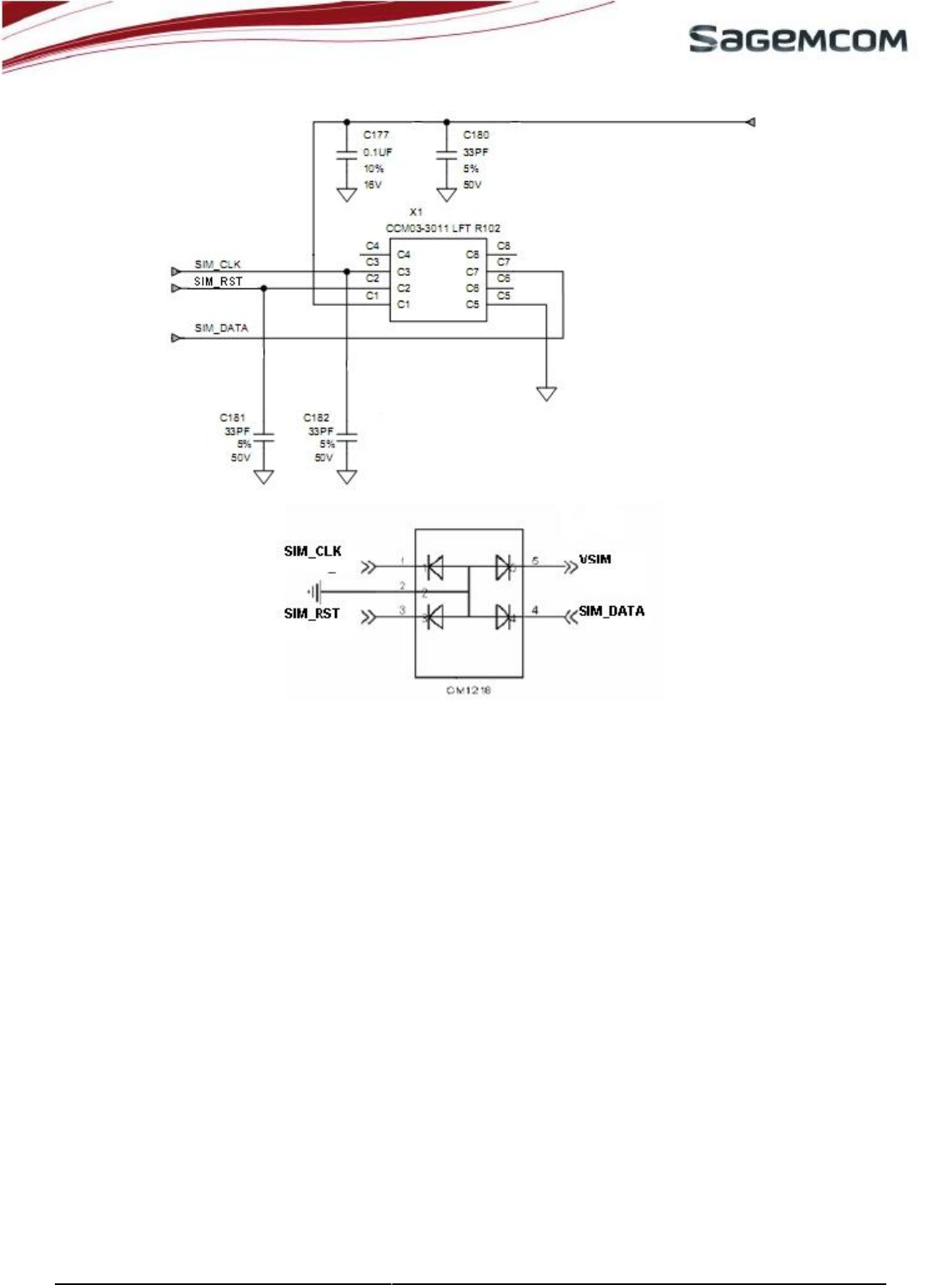
3.1.
How
to
connect
a
SIM
card
: SIM Card signals
The HILONC-3GPS module provides SIM signals to the 116 pins of the LGA. A SIM card holder with 6 pins
must be adopted to access SIM functions.
Decoupling
capacitors
must
be
added
on
to
the
VSIM,SIM_DATA,SIM_RST,and
SIM_CLK
signals
as
close
as possible to the SIM card connector to avoid EMC issues and in order to pass SIM card approval tests.
Vsim must be used only for the SIM card.
Use
ESD
protection
components
to
protect
the
SIM
card
and
module
I/Os
against
electrostatic
discharge.
The
following
schematic
shows
how
to
protect
SIM
access
of
the
6
pin
connector.
This
must
be
performed
every
time the SIM card holder is accessed by the end user.
Note d’étude / Technical document :
01/08/20111
-
Page
9
/
41
PIN No.
Name
C1
VCC
C2
RST
C3
CLK
C4
NA
C5
GND
C6
VPP
C7
I/O
C8
N/A
URD1
– OTL 5696.1–
022
/ 72740 Edition 0.4
HILONC-
3GPS
APPLICATION
NOTE
VSIM
: EMC and ESD protection components in the vicinity of the SIM
If it is necessary to use long SIM bus lines of over 100 mm, it is recommended to adopt serial resistors to
avoid
electrical
overshoot
on
SIM
bus
signals.
Use
56
for
the
clock
line
and
for
the
reset
and
data
lines.
Note d’étude / Technical document :
01/08/20111
-
Page
10
/
41
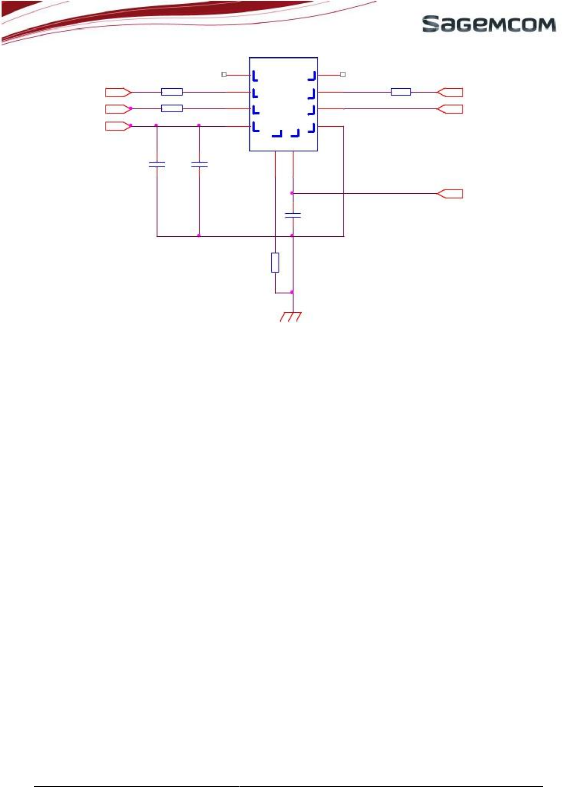
10
C601
10nF
C602
33pF
9
R616
2.2k
C60322pF
7
URD1
– OTL 5696.1–
022
/ 72740 Edition 0.4
HILONC-
3GPS
APPLICATION
NOTE
SIM_CLK_CARD
SIM_RST_CARD
R601
56
R602
10
NC
4
8
3
2
6
NC
R601
10
SIM_DATA_CARD
VSIM_CARD
VSIM_CARD
1
5
SIM_GPIO
GND
:
Serial
resistors
for
protection
of
long
SIM
bus
lines
The
schematic
above
includes
a
hardware
SIM
card
presence
detector.
It
can
be
connected
to
GPIO2.
GPIO2
is
the
design
default
for
SIM
card
detection.
Use
a
22pF
capacitor
to
debounce
the
GPIO2
detection
signal.
The
SIM
card
must
not
be
removed
from
its
holder
while
it
is
still
powered.
Switch
the
module
off
with
the
AT
command,
then
remove
the
SIM
card
from
its
holder.
3.2.
Audio
Connection
The
HILONC-3GPS
module
features
one
input
audio
path
and
one
output
audio
path.
The
input
path
is
a
PCM
digital
input.
The
output
path
is
a
PCM
digital
output.
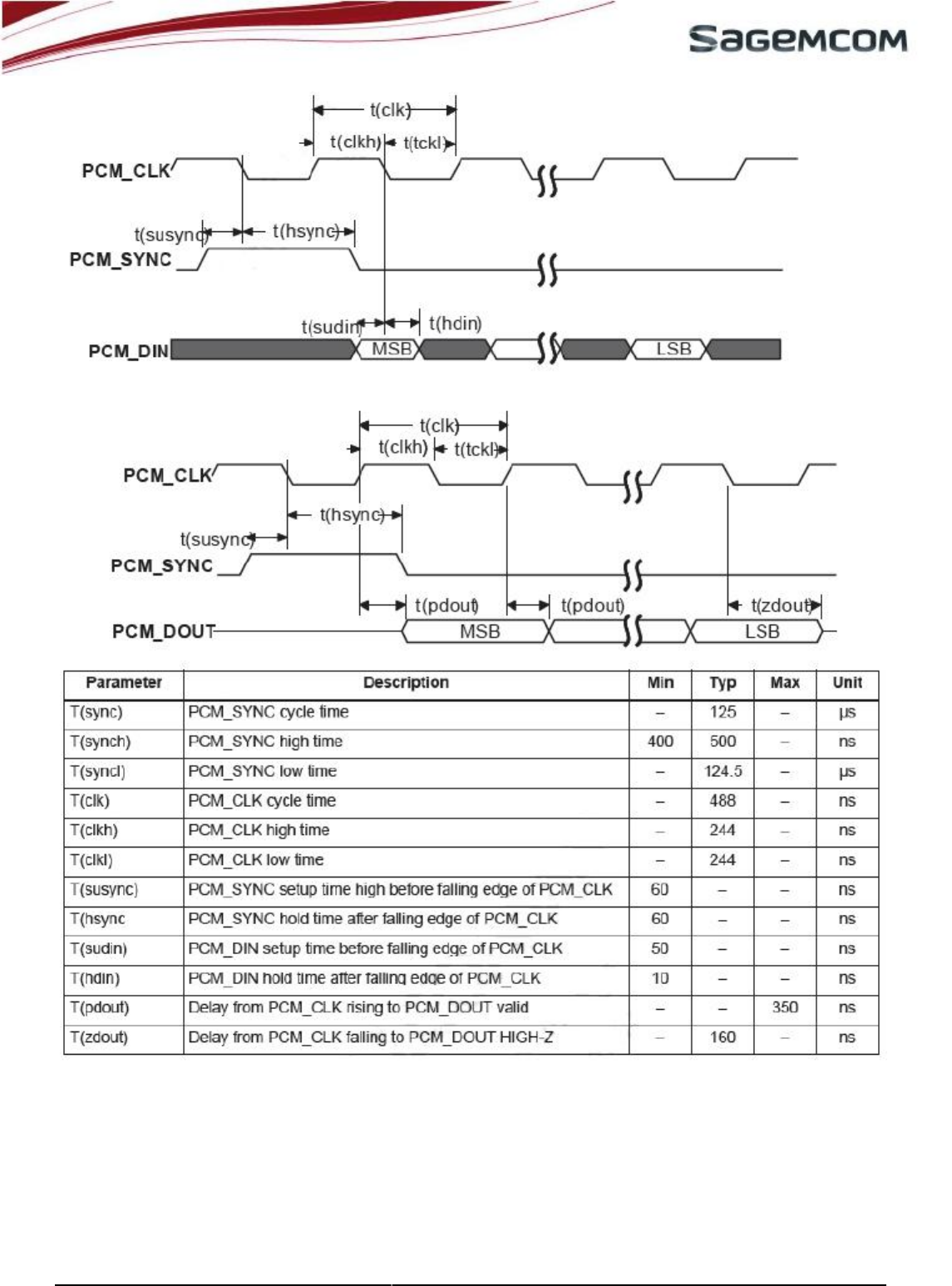
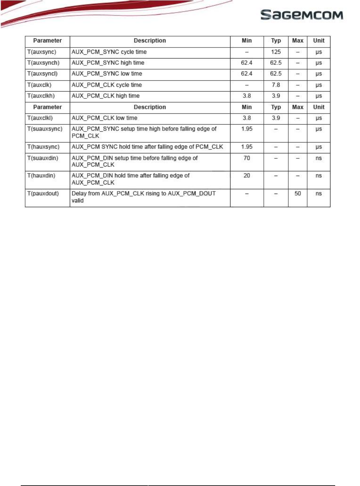
3.2.1.
PCM
Digital
Audio
HILONC-3GPS
can
be
used
for
connection
to
an
external
codec
through
the
integrated
PCM
interface.
The
interface
supports
an
8
kHz
short
sync
mode
at
2048
kHz
and
an
8
kHz
long
sync
mode
at
128
kHz.
In
short-
sync
(primary
PCM)
mode,
the
HILONC-3GPS
can
act
as
master
or
slave.
In
long-sync
(auxiliary
PCM)
mode,
the
HILONC-3GPS
is
always
a
master;
there
is
no
slave
support.
Note
d’étude
/
Technical
document
:
01/08/20111
-
Page
11
/
41
URD1
– OTL 5696.1–
022
/ 72740 Edition 0.4
HILONC-
3GPS
APPLICATION
NOTE
: Primary PCM mode timing parameter
Note d’étude / Technical document :
01/08/20111
-
Page
12
/
41
URD1
– OTL 5696.1–
022
/ 72740 Edition 0.4
HILONC-
3GPS
APPLICATION
NOTE
Note d’étude / Technical document :
01/08/20111
-
Page
13
/
41
URD1
– OTL 5696.1–
022
/ 72740 Edition 0.4
HILONC-
3GPS
APPLICATION
NOTE
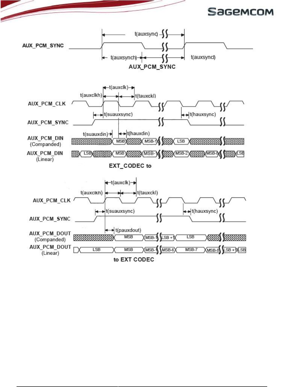
: Auxiliary PCM mode timing parameter
3.3.
PWM
A single PWM pin is available on the HILONC-3GPS. This is a general purpose PWM which can be used to
drive
a
vibrating
device,
keypad
backlight
or
LED.
The
PWM
pin
can
be
controlled
by
AT
commands,
allowing
several periods and duty cycles. More details are given in the AT commands specifications document.
PWM output can be set by the user:
Frequency between: 0.125Hz and 8KHz
Duty range from: 0 to 100%
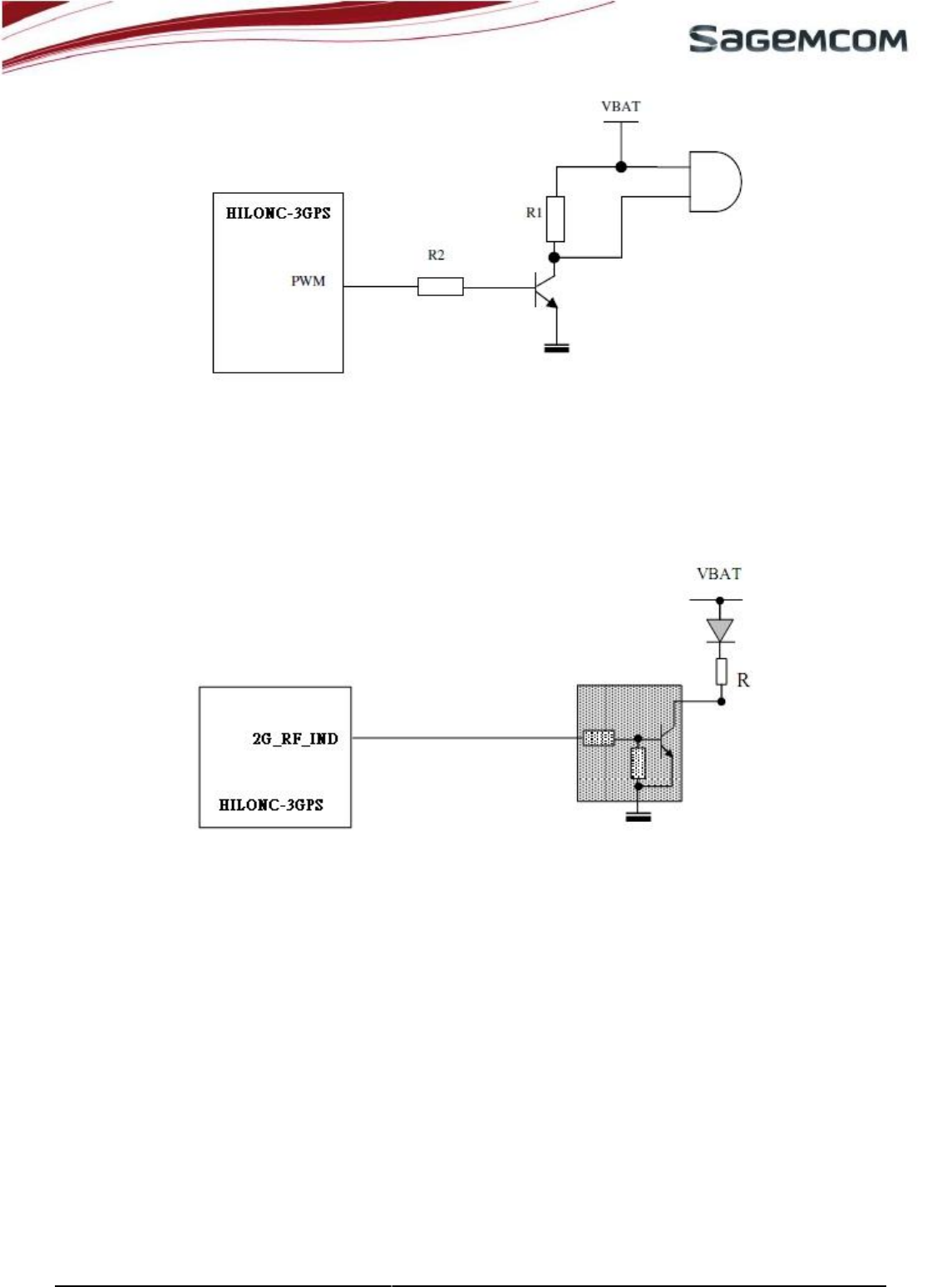
3.3.1.
PWM
for
Buzzer
connection
The
HILONC-3GPS
module
can
utilize
PWM
output
to
drive
a
buzzer.
The
buzzer
can
serve
as
an
abnormal
status alarm.
Resistors
must
be
added
to
protect
the
buzzer.
The
value
of
these
resistors
depends
on
the
buzzer
and
the
transistor. Normally, they are set at
Note d’étude / Technical document :
01/08/20111
-
Page
14
/
41
URD1
– OTL 5696.1–
022
/ 72740 Edition 0.4
HILONC-
3GPS
APPLICATION
NOTE
: Buzzer connection
3.3.2.
Network
LED
The HILONC-3GPS module can manage a network LED which can be connected to 2G_RF_IND.
The transistors can be found in a single package referred to as the UMDXX or PUMDXX Family.
The value of resistor R depends on the characteristics of the LED; its purpose is to limit the current passing
through the diode.
Use the AT command to set the 2G_RF_IND used to control the LED.
: Network LED connection
3.4.
Power
Requirements
Input Rating : 3.4V ~ 4.2VDC , 700mA , Operation Temperature : -40℃~85℃ .
The host system must supply 3.4V ~ 4.2Vof power to the VBAT.
Within normal 2G and 3G operational modes, the maximum average current is approximately 1.1A
depending on RF output power. In 2G mode peak current can be as high as 2A under matched antenna
conditions. Peak current could be as high as 1.75A in the case of a mismatched antenna. In 3G mode and
under conditions of antenna mismatch, peak current may increase by up to 700mA.
VBAT traces are required to be as short and as wide as possible.
VBAT
ceramic
decoupling
capacitors
of
at
least
are
required
to
ensure
good
RF
performance.
It
is strongly recommended to place capacitors close to the connection pad and connected via low
resistance tracks to VBAT and GND.
Host
power
must
be
capable
of
sourcing
enough
current
to
accommodate
maximum
power
in
the
event
of
2G transmission bursts. This can be done, for example, by adding a large capacitor with a low ESR value.
PCB
tracks
must
be
well
dimensioned
to
support
a
maximum
current
of
2.2A.
Voltage
ripple
caused
by
serial
resistance of the power supply path could result in instances of voltage drop.
The HILONC-3GPS does not support battery charging.
Note d’étude / Technical document :
01/08/20111
-
Page
15
/
41
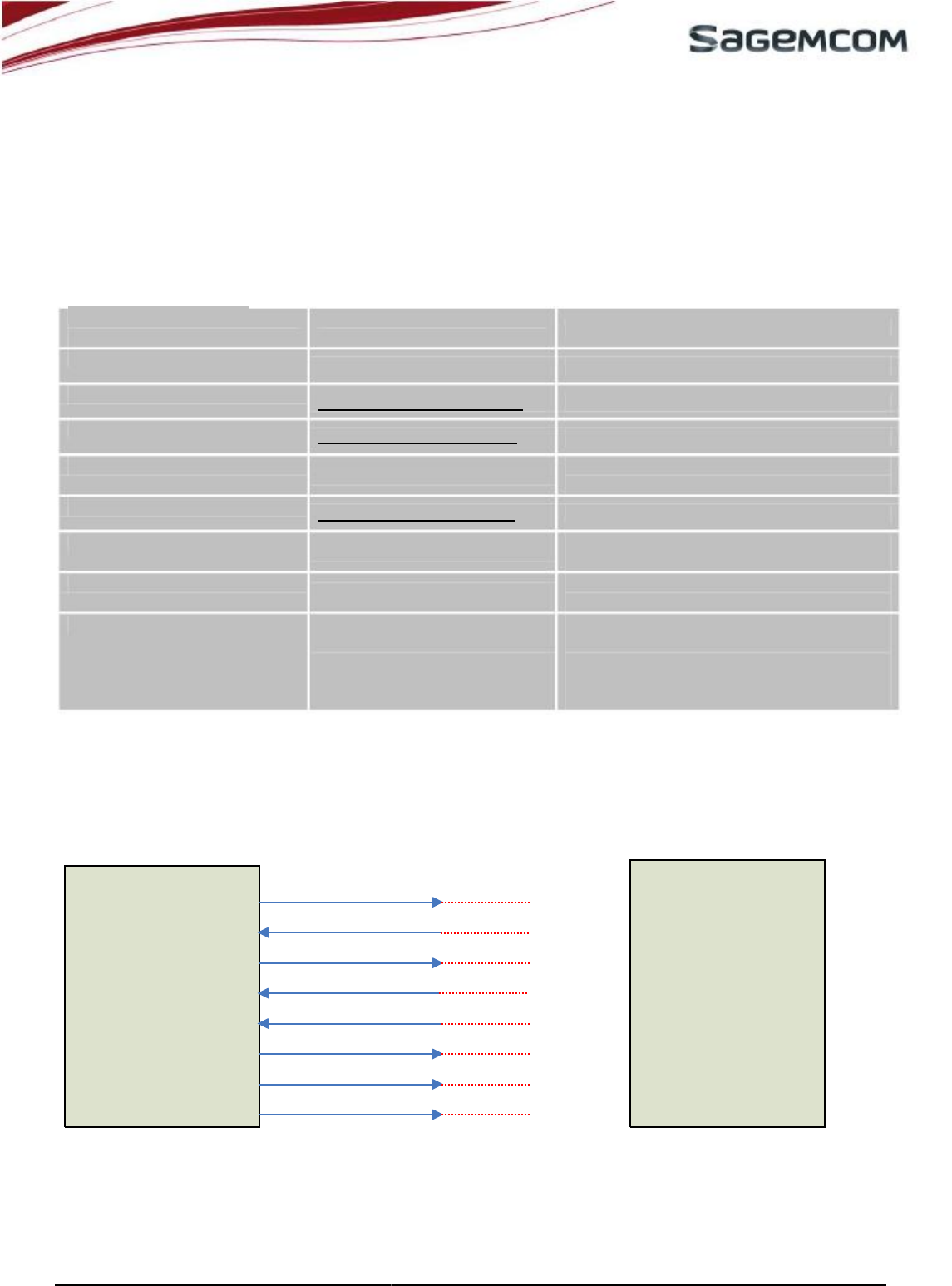
view)
Signal
name
(DTE
point
of
view)
Signal
use
(DTE
point
of
view)
DTE_DSR
Signal
UART
interface
is
ON
DTE_CTS HILONC-3GPS is ready to receive AT
DTE_RTS
Wakes
up
the
module
when
Ksleep=1
is
DTE_RI
Signal
incoming
calls
(voice
and
data),
URD1
– OTL 5696.1–
022
/ 72740 Edition 0.4
HILONC-
3GPS
APPLICATION
NOTE
3.5.
UART
The
HILONC-3GPS
has
a
UART
port
that
can
be
used
in
low-speed,
full-speed,
and
high-speed
modes.
The
UART
communicates
with
serial
data
ports
conforming
to
the
RS-232
interface
protocol.
With
a
properly
written
and
user-defined
download
program,
the
UART
port
can
be
used
for
testing
and
debugging.
Provision
of
external
access
to
the
V24
interface
for
easy
upgrade
of
software
is
recommended.
Baud
rate
up
to
4Mbps.
Unused
signals
remain
disconnected.
Signal name (DCE point of
UART_DTR
UART_DCD
UART_RX
UART_RTS
UART_TX
UART_CTS
UART_RI
UART_DSR
DTE_DCD
Signal
data
connection
in
progress
DTE_TX
Transmit
data
commands
DTE_RX
Receive
data
used
SMS,
etc.
Prevents
the
HILONC-3GPS
from
entering
sleep
mode
DTE_DTR
Switches
between
data
mode
and
command
mode
Wakes
the
module
up.
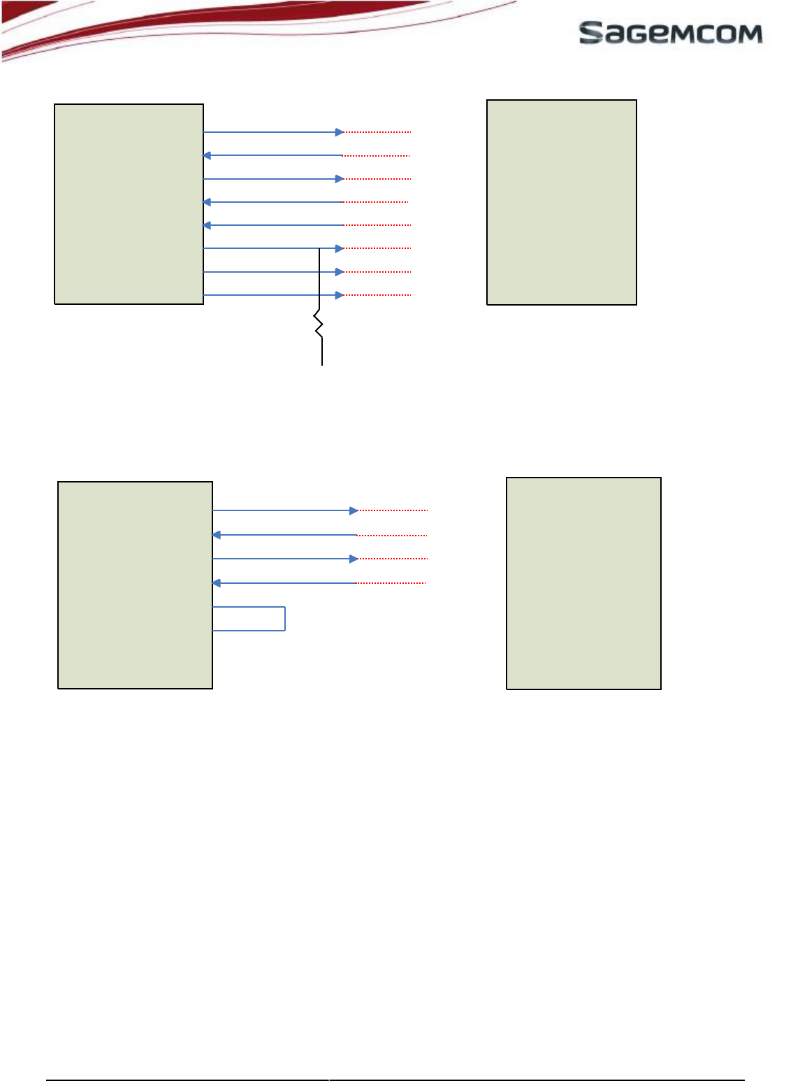
3.5.1.
Complete
V24
Connection
of
HILONC-3GPS
to
host
The
40
pins
of
the
HILONC-3GPS
module
provide
a
V24
interface
with
the
following
signals:
RTS/CTS,
RXD/TXD,
DSR,
DTR,
DCD,
RI.
Use
of
this
complete
V24
connection
is
required
whenever
your
application
exchanges
data.
HiLoNC-3GPS
pin60
pin17
pin59
pin16
pin15
pin14
pin58
pin61
UART1_TX
UART1_RX
UART1_RTS
UART1_CTS
UART1_DSR
UART1_DTR
UART1_DCD
UART1_RI
DTE_RX
DTE_TX
DTE_CTS
DTE_RTS
DTE_DTR
DTE_DSR
DTE_DCD
DTE_RI
DTE
device
GND
is
not
represented.
:
Complete
V24
connection
of
HILONC-3GPS
to
host
This
configuration
allows
the
use
of
flow
control
RTS
&
CTS
to
avoid
overflow
error
during
data
transfer.
In
addition,
UART_RTS
is
used
to
inform
DTE
whether
the
HILONC-3GPS
is
ready
to
receive
an
AT
command
after
power
up
sequence
or
wake
up
from
the
sleep
mode.
Note
d’étude
/
Technical
document
:
01/08/20111
-
Page
16
/
41
OUT
IN
URD1
– OTL 5696.1–
022
/ 72740 Edition 0.4
HILONC-
3GPS
APPLICATION
NOTE
TBD
:
RTS
versus
PWRON
signal
during
power
on
sequence
This
signal
configuration
also
enables
all
signals:
·
UART_RI
signal
is
used
when
programmed
to
indicate
an
incoming
voice
or
data
call
or
SMS
incoming
message,
etc.
·
UART_DCD
signal
is
used
to
indicate
GPRS
connections.
·
UART_DTR
signal
is
used
to
indicate
that
the
module
UART
interface
is
ON.
·
UART_DSR
signal
is
used
to
prevent
the
HILONC-3GPS
from
entering
sleep
mode,
switching
between
Data
and
AT
commands,
hanging
up
a
call
or
waking
up
the
module
etc.
Avoid
supplying
power
to
the
UART
before
the
HILONC-3GPS
is
ON,
as
this
may
result
in
power
up
sequence
error.
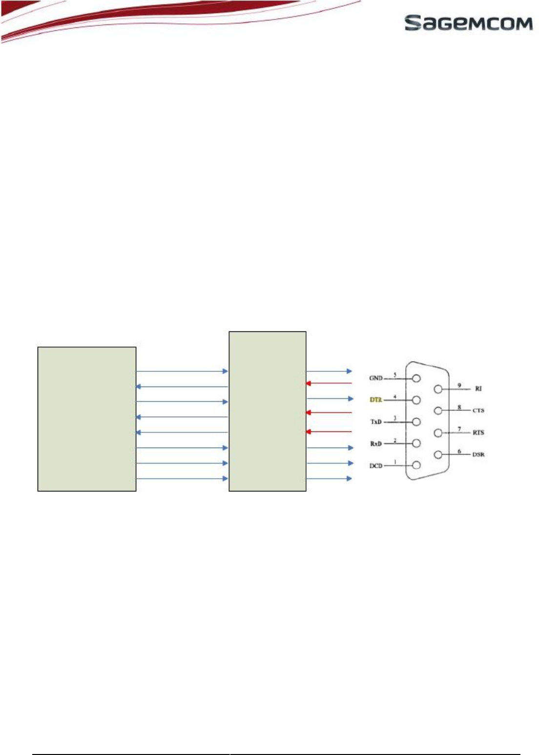
3.5.2.
Complete
V24
Interface
with
PC
To
use
the
V24
interface
some
adaptation
of
components
is
necessary.
This
is
because
HILONC-3GPS
signals
need
to
be
converted
to
+/-
5V
signals
compatible
with
a
PC.
RS232
HiLoNC3GPS
pin60
pin17
pin59
pin16
pin15
pin14
pin58
pin61
UART1_TX
UART1_RX
UART1_RTS
UART1_CTS
UART1_DSR
UART1_DTR
UART1_DCD
UART1_RI
Transceiver
IN
OUT
IN
OUT
OUT
IN
OUT
IN
IN
OUT
IN
OUT
IN
OUT
RXD
TXD
CTS
RTS
DTR
DSR
DCD
RI
SUBD9
Female
GND
is
not
represented.
Note:
pin
5
is
GND
:
Connection
to
a
data
cable
Avoid
supplying
power
to
the
UART
before
the
HILONC-3GPS
is
ON,
as
this
could
result
in
power
up
sequence
error.
UART_DTR
signal
used
to
indicate
module
UART
interface
is
ON
(need
to
pull
high
the
UART_DTR
signal
with
470
K
ohms
to
external
3V,
as
shown
below):
Note
d’étude
/
Technical
document
:
01/08/20111
-
Page
17
/
41
URD1
– OTL 5696.1–
022
/ 72740 Edition 0.4
HILONC-
3GPS
APPLICATION
NOTE
GND
is
not
reprenested.
HiLoNC3GPS
pin60
pin17
pin59
pin16
pin15
pin14
pin58
pin61
UART1_TX
UART1_RX
UART1_RTS
UART1_CTS
UART1_DSR
UART1_DTR
UART1_DCD
UART1_RI
DTE_RX
DTE_TX
DTE_CTS
DTE_RTS
DTE_DTR
DTE_DSR
DTE_DCD
DTE_RI
DTE
device
470K
External
1.8V
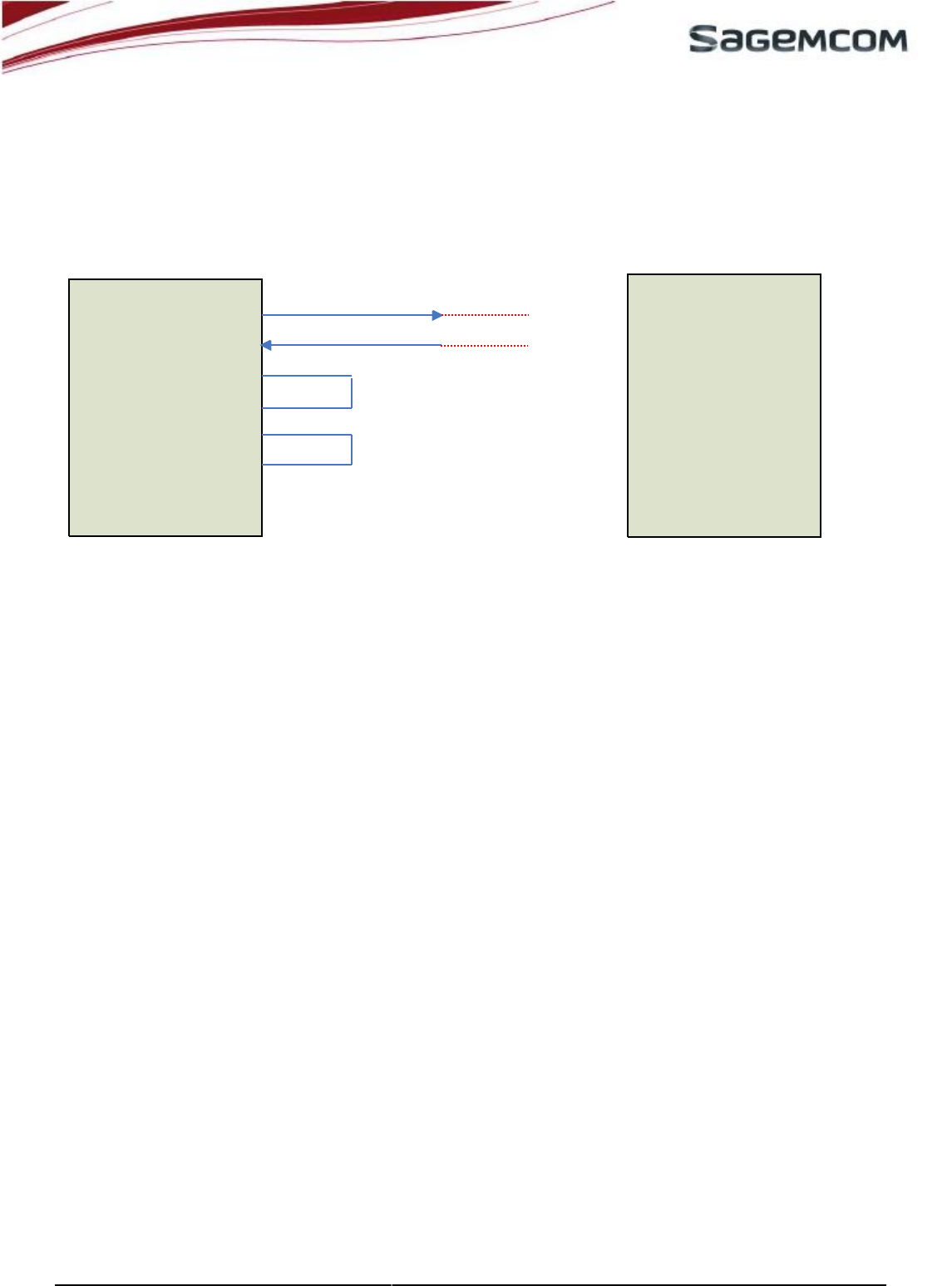
3.5.3.
Partial
V24
(RX-TX-RTS-CTS)
Connection
of
HILONC-3GPS
to
host
When
using
only
RX/TX/RTS/CTS
instead
of
the
complete
V24
link,
the
following
schematic
can
be
used:
HiLoNC3GPS
pin60
pin17
pin59
pin16
UART1_TX
UART1_RX
UART1_RTS
UART1_CTS
DTE_RX
DTE_TX
DTE_CTS
DTE_RTS
DTE
device
UART1_DSR
pin15
UART1_DTR
pin14
UART1_DCD
pin58
NC
UART1_RI
pin61
NC
GND
is
not
represented.
:
Partial
V24
connection
(4
wires)
of
HILONC-3GPS
to
host
As
UART_DTR
is
active
(low
electrical
level)
once
HILONC-3GPS
is
switched
on,
UART_DSR
is
also
active
(low
electrical
level),
therefore
the
AT
command
AT+Ksleep
can
switch
between
the
two
sleep
modes
availableHILONC.
UART_DCD
and
UART_RI
can
remain
disconnected
and
floating
when
not
in
use.
Otherwise
use
to
pull
power
up
to
1.8V.
This
configuration
allows
use
of
flow
control
RTS
&
CTS
to
avoid
overflow
error
during
data
transfer.
Moreover
UART_RTS
is
used
to
indicate
when
the
HILONC-3GPS
module
is
ready
to
receive
an
AT
command
after
power
up
sequence
or
wake
up
from
sleep
mode.
However
this
configuration
does
not
allow
signals
such
as:
·
UART_RI
signal
used
when
programmed
to
indicate
an
incoming
voice
or
data
call
or
incoming
SMS
.
·
UART_DCD
signal
used
to
indicate
DATA
connections.
·
UART_DTR
signal
used
to
indicate
module
UART
interface
is
ON.
Note
d’étude
/
Technical
document
:
01/08/20111
-
Page
18
/
41
URD1
– OTL 5696.1–
022
/ 72740 Edition 0.4
HILONC-
3GPS
APPLICATION
NOTE
·
The
UART_DSR
signal
is
used
to
prevent
HILONC-3GPS
from
entering
sleep
mode
or
to
switch
between
DATA
and
AT
commands
or
to
hang
up
a
call
or
to
wake
up
the
module
.
3.5.4.
Partial
V24
(RX-TX)
Connection
of
HILONC-3GPS
to
host
When
using
only
RX/TX
instead
of
the
complete
V24
link
the
following
schematic
can
be
used:
HiLoNC3GPS
pin60
pin17
UART1_TX
UART1_RX
DTE_RX
DTE_TX
DTE
device
UART1_RTS
pin59
UART1_CTS
pin16
UART1_DSR
pin15
UART1_DTR
pin14
UART1_DCD
pin58
NC
UART1_RI
pin61
NC
GND
is
not
represented.
:
Partial
V24
connection
(2
wires)
of
HILONC-3GPS
to
host
As
UART_DTR
is
active
(low
electrical
level)
once
HILONC-3GPS
is
switched
on,
UART_DSR
is
also
active
(low
electrical
level),
therefore
the
AT
command
AT+Ksleep
can
switch
between
the
two
available
sleep
modesHILONC.
As
UART_RTS
is
active
(low
electrical
level)
once
HILONC-3GPS
is
switched
on,
UART_CTS
is
also
active
(low
electrical
level),
therefore
the
AT
command
AT+Ksleep
can
switch
between
the
two
available
sleep
modesHILONC.
The
HILONC-3GPS's
firmware
allows
activation
of
UART_RTS
during
sleep
state
even
when
looped
to
the
UART_CTS
signal.
UART_DCD
and
UART_RI
can
remain
disconnected
and
floating
when
not
in
use.
Note
that
this
configuration
does
not
allow
the
below
signals:
·
RI
signal
used
when
programmed
to
indicate
an
incoming
voice
or
data
call
or
incoming
SMS
.
·
UART_DCD
signal
used
to
indicate
GPRS
connections.
·
UART_DTR
signal
used
to
indicate
the
module
UART
interface
is
ON.
·
UART_DSR
signal
used
to
prevent
the
HILONC-3GPS
module
from
entering
sleep
mode.
3.6.
GPIO
There
are
six
GPIOs
available
on
the
HILONC-3GPS.
Customer
applications
can
directly
access
them
through
appropriate
AT
commands
such
as:
-
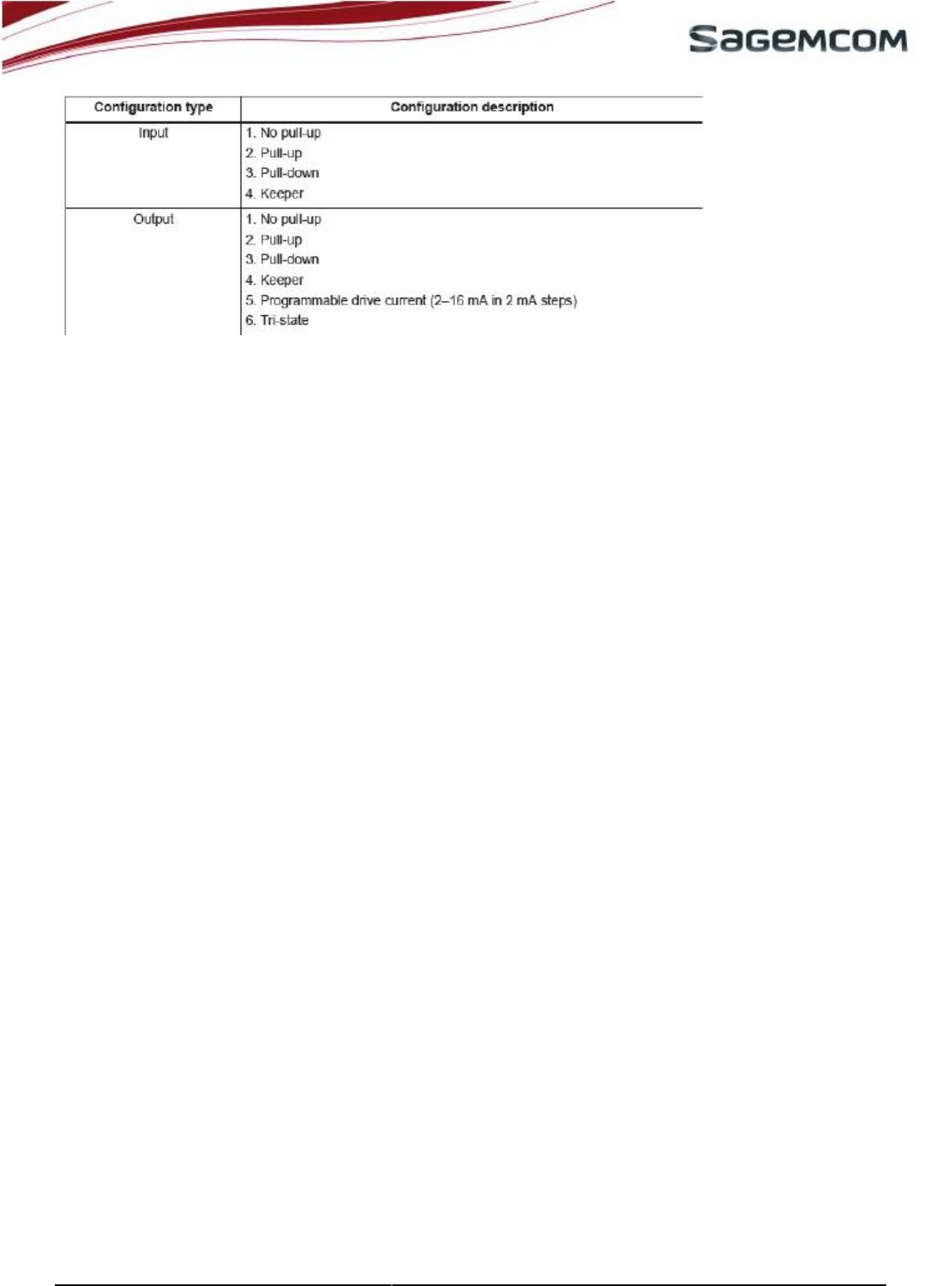
Output:
pin
is
set
to
High
or
Low
state.
-
Input:
pin
is
read
on
request
and
customer
application
is
responded
to.
As
an
input
different
scenarios
are
possible
to
cover
a
maximum
range
of
customer
applications:
·
Synchronous
answer
to
AT
command.
·
Asynchronous
answer
to
AT
command.
Customer
application
prior
to
the
read
request
has
configured
the
GPIO
to
react
to
falling/rising
edges.
The
customer
application
is
notified
asynchronously
by
AT
command
answer
when
the
configured
trigger
occurs.
Note
d’étude
/
Technical
document
:
01/08/20111
-
Page
19
/
41
URD1
– OTL 5696.1–
022
/ 72740 Edition 0.4
HILONC-
3GPS
APPLICATION
NOTE
: Programmable GPIO configurations
By utilizing other special AT commands, GPIOs can be used to, for example:
1. Perform I/O toggling while the module is attached to the network.
2. Perform I/O toggling when a pre-set temperature is reached.
3. Serve as an input to detect the presence of an antenna (with some additional external power.)
4. GPIO2 serves as an input default to detect SIM card presence .
3.7.
ADC
The HILONC-3GPS has one ADC input pin which can be used to read the value of the voltage applied. The
following conditions must be met to ensure correct performance:
· Input signal voltage must be within 0V to 2.1V.
· Input impedance of the pin is .
· Input capacitance typically is 53pF.
The AT command AT+KADC will produce a voltage value with the following characteristics:
· 15 bits resolution
· Maximum sampling frequency of 2.4MHz.
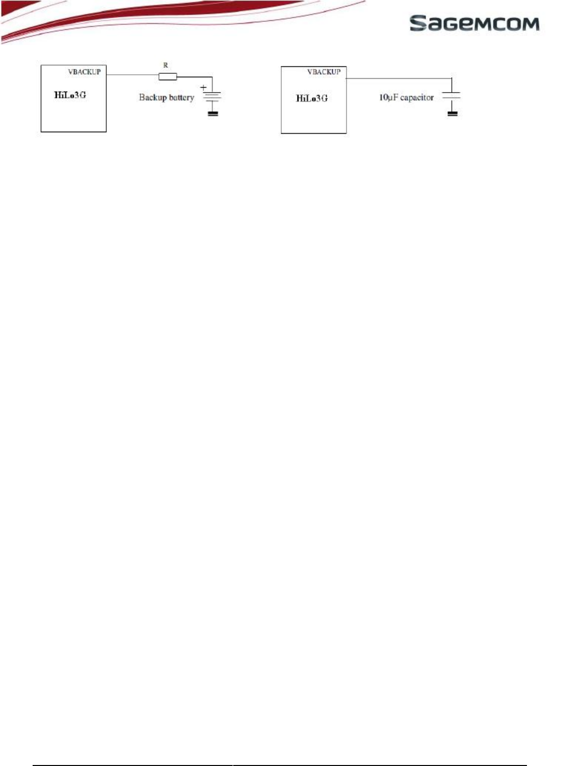
3.8.
Backup
Battery
3.8.1.
Backup
Battery
Function
Features
A
backup
battery
can
be
connected
to
the
module
in
order
to
supply
internal
RTC
(Real
Time
Clock)
when
the
main
power
supply
is
removed.
Thus,
when
the
main
power
supply
is
removed,
the
RTC
is
still
supplied
with
power and the module keeps the time register running.
·
If VBAT < 3V, internal RTC is supplied by VBACKUP.
· If VBAT 3V, internal RTC is supplied by VBAT.
3.8.2.
Internal
HILONC-3GPS
Charging
Function
HILONC-3GPS has a charging function that does not require any additional external power supply (power
supply for the charging is provided by the HILONC-3GPS).
Charge of the back-up battery occurs only when main power supply VBAT is provided.
Note d’étude / Technical document :
01/08/20111
-
Page
20
/
41
URD1
– OTL 5696.1–
022
/ 72740 Edition 0.4
HILONC-
3GPS
APPLICATION
NOTE
: Internal charging of backup battery or capacitor
The value of resistor R depends on the charging current value of the backup battery manufacturer.
3.8.3.
Backup
Battery
Technology
Capacitor batteries do not have the disadvantages of lithium ion rechargeable batteries:
· Maximum discharge current is generally greater,
· No need to regulate charge current.
Moreover, this kind of battery is available in the same kind of package as a lithium ion cell and is fully
compatible
from
a
mechanical
perspective.
The
only
disadvantage
is
that
the
capacity
is
significantly
lower
than
a manganese silicon lithium ion battery.
3.9.
USB
The
HILONC-3GPS
module
has
a
set
of
USB_DP
and
USB_DN
bi-directional
differential
USB
data
lines
that
comply with USB 2.0 specifications.
HILONC-3GPS acts as the USB-Slave and the customer application acts as the USB-Master.
· Integrated high-speed USB PHY.
· In compliance with USB 2.0 specifications for a peripheral device.
·The
USB
2.0
specification
requires
hosts
such
as
PCs
to
support
all
three
USB
speeds,
namely
low-speed
(1.5
Mbps),
full-speed
(12
Mbps)
and
high-speed
(480
Mbps).
The
USB
2.0
specification
allows
peripheral
devices
to
support any one or more of these speeds.
The USB_DP and USB_DN signals are routed as a ~90 differential pair. These signals must be routed
side by side and on the same layer and their trace length should be matched as closely as possible.
A 2pF capacitor is required to be installed between USB_DP and USB_DN close to the HILONC-3GPS.
These
signals
have
relatively
fast
edges,
so
they
should
be
routed
away
from
sensitive
circuits
and
signals
such
as
19.2
MHz
TCXO,
sleep
XTAL,
and
RF.
Therefore,
avoid
routing
these
signals
on
surface
layers;
routing
in the inner layer sandwiched between power and ground is preferable.
4.
Power
Management
The host system should supply 3.4V~4.2V to VBAT for powering the baseband, logics circuit and RF circuit.
4.1.
Power
Modes
Depending on the status of the HILONC-3GPS, different power consumption modes can be identified.
Active mode (Active communication)
All
systems
on
HILONC-3GPS
are
active.
In
this
mode,
the
module
is
registered
to
the
network
and
a
voice/data
Note d’étude / Technical document :
01/08/20111
-
Page
21
/
41

URD1
– OTL 5696.1–
022
/ 72740 Edition 0.4
HILONC-
3GPS
APPLICATION
NOTE
call
is
actively
transmitting
data.
Sleep
mode
(Active
idle)
All
systems
on
HILONC-3GPS
are
active
including
the
USB
bus.
In
this
mode,
the
module
is
registered
to
the
network
but
it
is
idle/paging
only.
No
voice/data
call
connection
is
established.
Fly
mode
The
processor
is
still
active
but
the
radio
section
is
powered
down.
This
mode
can
be
controlled
by
sending
an
AT
command
to
the
module.
4.2.
Module
Power
up
Starting
the
HILONC-3GPS
via
PWON.
4.2.1.
PWON
Power
up
To
start
the
module,
first
power
up
VBAT,
which
must
be
in
the
range
3.4V
~
4.2V,
and
must
be
able
to
supply
1.75A
during
TX
bursts.
PWON
is
a
low
level
active
signal
internally
pulled
up
to
a
dedicated
power
domain
of
1.8V.
As
PWON
is
internally
pulled
up,
a
simple
open
collector
or
open
drain
transistor
must
be
used
for
ignition.
To
start
the
module,
a
low
level
pulse
must
be
applied
on
PWON
for
500ms.
After
a
few
seconds,
the
UART_RTS
enters
active
state
and
the
module
is
ready
to
receive
AT
commands.
VGPIO
is
a
supply
output
from
the
module
that
can
be
used
to
check
if
the
module
is
active.
·
When
VGPIO
=
0V
the
module
is
OFF.
·
When
VGPIO
=
2.85V
the
module
is
ON.
TBD
:
Power
on
sequence
TBD
:
Power
off
sequence
Send
AT
COMMAND
to
power
off
module.
4.2.2.
IO
DC
Presence
before
Power
on
When
VBAT
is
available
but
the
module
has
not
yet
powered
up,
the
following
I/O's
raise
their
output.
VBACKUP
raise
to
3V
PWON
raise
to
1.8V
4.3.
Power
on
and
Sleep
Diagrams
The
2
diagrams
below
show
the
behavior
of
the
module
and
the
DTE
during
power
on
and
then
in
sleep
modes.
Note:
the
module
cannot
enter
sleep
mode
if
USB
bus
is
connected.
TBD
:
Diagram
for
power
on
TBD
:
Diagram
for
sleep
mode
4.4.
Module
Power
off
Note
d’étude
/
Technical
document
:
01/08/20111
-
Page
22
/
41
URD1
– OTL 5696.1–
022
/ 72740 Edition 0.4
HILONC-
3GPS
APPLICATION
NOTE
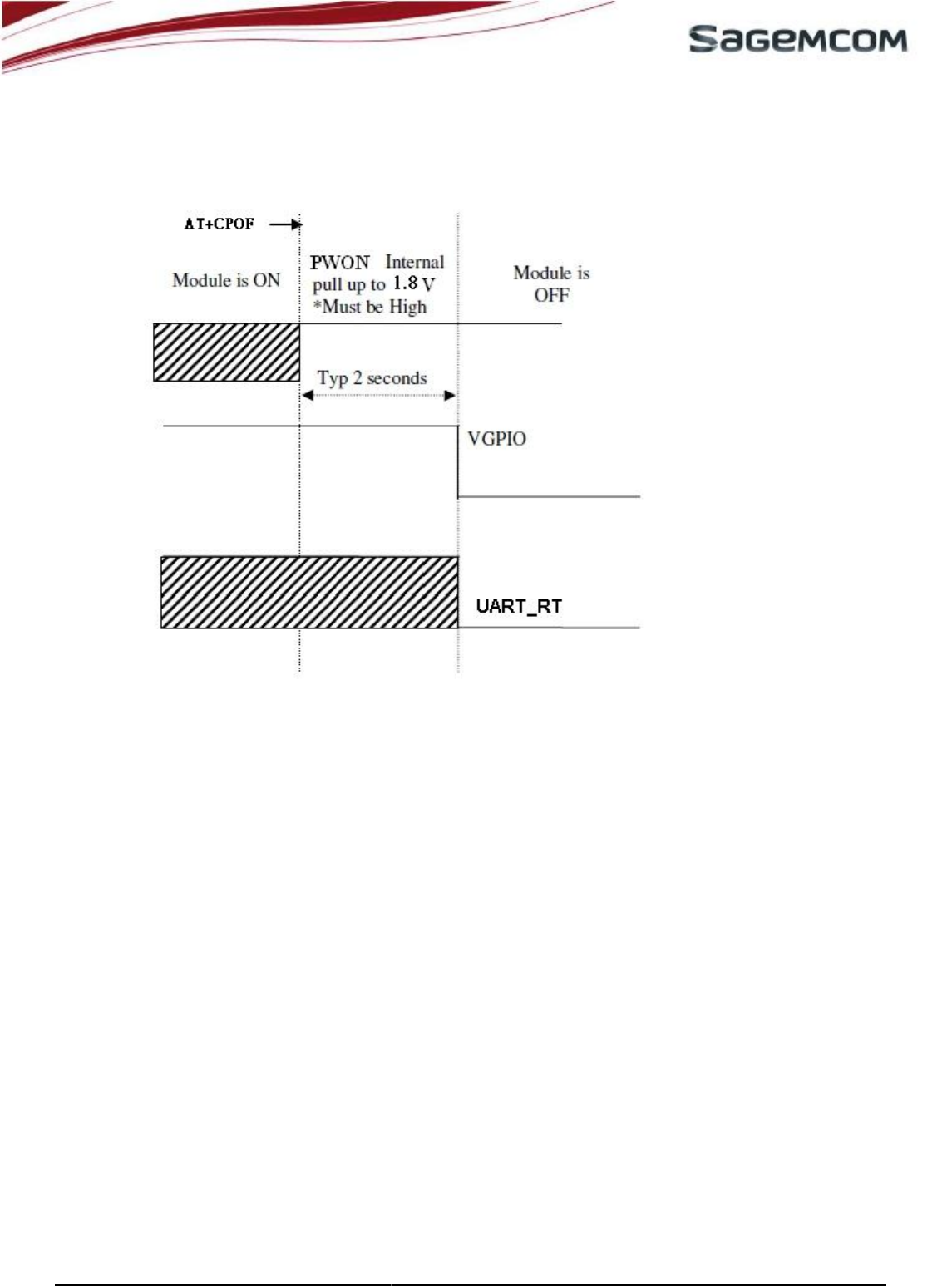
4.4.1.
UART
Interface
To
turn
the
module
off,
use
the
AT
command
AT+CPOF.
If
PWON
is
not
pulled
down
the
module
will
switch
to
OFF
mode
after
the
AT
command,
otherwise
the
module
restarts
immediately
(OFF
sequence
is
performed
followed by power ON sequence).
: Power off sequence for PWON, VGPIO and UART_RTS
4.4.2.
USB
Interface
As
the
module
can
also
be
turned
on
when
a
USB
cable
is
plugged
in,
the
module
turn
off
sequence
requires
the
USB
interface
to
be
OFF
or
VBUS
disconnected
once
the
command
is
sent
and
acknowledged
by
the
module.
Thus,
to
turn
the
module
off
when
USB
interface
is
in
use,
use
the
AT
command
AT+CPOF,
then
disconnect
VBUS
signal
(unplug
the
USB
cable
or
use
a
command
switch
to
switch
off
VBUS)
when
the
module
acknowledges
(responds
with
an
OK
message)
the
command,
otherwise
the
module
will
restart
immediately
(an
OFF sequence is performed followed by a power ON sequence).
4.5.
Sleep
Mode
The AT command AT+KSLEEP allows configuration of the sleep mode.
When AT+KSLEEP=1 has been configured:
· The HILONC-3GPS module decides by itself when to enter sleep mode (no tasks running).
· character on serial link wakes up the HILONC-3GPS module.
When AT+KSLEEP=0 has been configured:
· The HILONC-3GPS module is active when UART_DSR signal is active (low electrical level).
·
When
UART_DSR
is
deactivated
(high
electrical
level),
the
HILONC-3GPS
module
enters
sleep
mode
after
a
certain period of time.
· On UART_DSR activation (low electrical level), the HILONC-3GPS module wakes up.
When AT+KSLEEP=2 has been configured:
· The HILONC-3GPS module is prevented from ever entering sleep mode.
In
sleep
mode
the
module
reduces
power
consumption
and
waits
for
a
wake
up
signal
from
either
the
network,
Note d’étude / Technical document :
01/08/20111
-
Page
23
/
41
URD1
– OTL 5696.1–
022
/ 72740 Edition 0.4
HILONC-
3GPS
APPLICATION
NOTE
from the operating system or from the host controller.
Note: The module cannot enter sleep mode if USB bus is connected.
5.
ESD
&
EMC
Recommendations
Adopting
the
Human
Body
Model
of
the
JEDEC
JESD
22-A114
standard,
the
HILONC-3GPS
can
support
2KV
on each LGA pad.
5.1.
HILONC-3GPS
Handling
HILONC-3GPS modules are packaged in boxes.
HILONC-3GPS
modules
contain
electronic
circuits
sensitive
to
the
electrostatic
electricity
of
the
human
hand.
Handling without ESD protection could result in permanent damage or even destruction of the module.
5.2.
ESD
Recommendations
If cust design requires the ability to withstand more than 2KV of electrostatic discharge, the following
must be observed:
ESD current is able to penetrate into the device via the following typical components:
· SIM connector
· Battery / data connector
· All parts with conductive paint.
as
much
as
possible
try
to
decrease
the
level
of
ESD
current
on
electronic
components located inside the device board, HILONC-3GPS inputs,
5.2.1.
Avoiding
ESD
HILONC-3GPS to the board.
ould be shielded and FPC connectors should be correctly grounded at each extremity.
Put
a
100nF
capacitor
to
the
battery,
or
even
better
put
a
varistor
or
ESD
diode
in
parallel
on
battery
and
charger wires (if any) and on all power wires connected to the module.
Following are the pin numbers to be protected from discharge of over 2KV and the varistor references.
Pin29/43/44: VBAT
Pin67/68/69: USB
Pin71: VGPIO
Pin33/34/35/79: USIM
5.3.
EMC
recommendations
To
avoid
EMC
issues,
place
the
capacitors
or
filters
as
close
as
possible
to
high
speed
data
lines
such
as
USB
and SDIO.
6.
Radio
Integration
Note d’étude / Technical document :
01/08/20111
-
Page
24
/
41
Part
Vendor
Part number
Varistor
LITTLEFUSE
V0402MHS12NR
Varistor (for USB line)
COOPER
0402ESDA-MLP1
URD1
– OTL 5696.1–
022
/ 72740 Edition 0.4
HILONC-
3GPS
APPLICATION
NOTE
The
HILONC-3GPS
module
incorporates
RF
transceiver
technology
that
converts
received
signals
directly
from
RF-to-baseband and transmits signals directly from baseband-to-RF (known as direct conversion or zero
intermediate
frequency
(ZIF)
processing).
This
technique
eliminates
the
need
for
large
IF
surface
acoustic
wave
(SAW) filters and supporting IF and LO circuits.
6.1.
Antenna
Connection
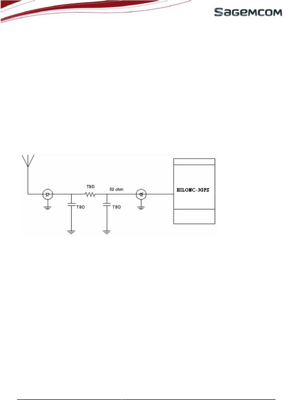
The HILONC-3GPS module is equipped with an RF LGA pad for antenna connection.
Definition of the reference antenna connector:
· Strictly 50 ohms matched impedance PCB tracks
· Straight PCB tracks
Antenna gain:
· Radiation pattern: depending on antenna position and size of device
· Gain average in space in all frequencies: > -3dBi
· Maximum VSWR: < 1.5:1 with 50 ohm reference impedance
In
order
to
achieve
optimum
sensitivity
and
output
power,
it
is
recommended
to
implement
a
matching
circuit
between the module and the antenna:
: Antenna connection reference
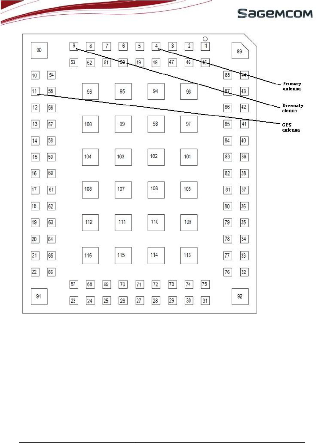
6.1.1.
Antenna
Pad
Three
50
ohm
RF
pads
on
the
HILONC-3GPS
PCB
are
available
for
antenna
connection.
One
is
for
the
Primary
antenna, the second is for Diversity RX and the other is for GPS antenna.
Note d’étude / Technical document :
01/08/20111
-
Page
25
/
41
URD1
– OTL 5696.1–
022
/ 72740 Edition 0.4
HILONC-
3GPS
APPLICATION
NOTE
: RF pads
6.1.2.
Antenna
Recommendations
Antenna
for
HILONC-3GPS
should
resonate
in
the
operating
bands
(GSM
850,
900,
1800,
1900
+
UMTS
band 1, 8) depending on the actual application of the specific HILONC-3GPS module.
Note that the RF-impedance of the HILONC-3GPS is 50.
Use low loss antenna cable (max. 0.5dB).
To
avoid
interference
choose
an
antenna
type
with
a
radiation
pattern
that
does
not
interfere
with
the
module. .
Circular polarized antennas are preferable.
Verify operation of the antenna by measuring the total radiated power.
Avoid placing a transmitting antenna near sensitive areas.
Apply EMC-design rules and follow shielding concepts.
Note d’étude / Technical document :
01/08/20111
-
Page
26
/
41

URD1
– OTL 5696.1–
022
/ 72740 Edition 0.4
HILONC-
3GPS
APPLICATION
NOTE
Keep
EMC-sensitive
and
high-emission
areas
separate.
6.2.
Ground
Link
Area
Good
ground
contact
between
the
module
and
board
is
required
to
achieve
optimum
radio
performance
(spurious,
All
HILONC-3GPS
ground
pads
must
be
connected
to
the
ground
of
the
board.
The
thermal
ground
pads
(pads
93~113)
must
be
soldered
to
the
ground
of
the
board
to
achieve
better
thermal
dissipation.
TBD
:
Thermal
pads
6.3.
Layout
Isolate
RF
line
and
antenna
from
other
bus
or
signals
Signals
should
avoid
being
in
the
vicinity
of
50
ohms.
If
not
possible,
add
ground
shielding
using
different
layers.
Do
not
add
any
ground
layer
under
the
antenna
contact
area.
Do
not
add
unvarnished
layout
traces
on
the
first
layer
of
the
customer
board,
or
unvarnished
via
holes
under
the
module
shield
area
or
it
will
result
in
short
circuit
of
those
signals.
This
is
mandatory.
Free
CAD
software
can
be
used
to
calculate
the
stack-up
parameters
to
ensure
a
compliant
50
ohm
RF
track.
6.4.
Mechanical
Recommendations
Do
not
apply
mechanical
pressure
on
the
HILONC-3GPS
shield.
Doing
so
could
damage
the
mechanical
structure
of
the
shield
and
lead
to
internal
short-circuits
or
other
issues.
Avoid
having
metallic
parts
in
the
vicinity
of
the
antenna
area.
Keep
FPCs
and
battery
contact
(if
any)
away
from
antenna
area.
FPC's
(if
any)
have
to
be
shielded.
6.5.
Other
Recommendation
-
production/design
test
Sagemcom
guarantees
RF
performance
in
conductive
mode
but
strongly
recommends
carrying
out
RF
measurements
in
an
anechoic
chamber
in
radiated
mode
(test
conditions
for
FTA):
radiated
performance
relies
heavily
on
radio
integration
(layout,
antenna,
matching
circuit,
ground
.)
7.
Audio
Integration
The
HILONC-3GPS
module
provides
only
a
digital
PCM
interface
for
audio.
A
PCM
codec
must
be
put
in
board
if
analog
audio
is
required.
The
audio
specifications
which
describe
the
audio
tests
are
3GPP
TS
26.131
&
3GPP
TS
26.132.
7.1.
Mechanical
integration
and
acoustics
Particular
care
of
Handset
Mode:
To
achieve
a
more
ideal
audio
output
design
(speaker
part):
The
speaker
must
be
completely
sealed
on
the
front
side.
The
front
aperture
must
in
compliance
with
specifications
of
the
speaker
supplier.
The
back
volume
must
be
completely
sealed.
Note
d’étude
/
Technical
document
:
01/08/20111
-
Page
27
/
41

URD1
– OTL 5696.1–
022
/ 72740 Edition 0.4
HILONC-
3GPS
APPLICATION
NOTE
The sealed back volume must be in compliance with specifications of the speaker supplier.
Pay attention to the design of the speaker gasket (elastomer).
Make sure to leave sufficient space for the artificial ear gasket.
To achieve a more ideal audio input design (microphone part) :
Pay attention to the design of the microphone (elastomer).
All receivers must be completely sealed on the front side.
Microphone
sensitivity
depends
on
the
shape
of
the
device
but
should
be
in
the
region
of
40
±3
dBV/Pa.
Encourage the use of a pre-amplified microphone. If needed, use a pre-amplification stage.
As audio input and output are strongly linked:
Place the microphone and the speaker as far away as possible from one another.
7.2.
Electronics
and
layout
Avoiding Distortion & Burst Noise
Audio signals must be symmetric (same components on each path).
Differential signals must be routed in parallel.
Audio layer must be surrounded by 2 ground layers.
The link from one component to the ground must be as short as possible.
If possible separate the PCBs of the microphone and speaker.
Reduce the number of electronic components as much as possible (to avoid loss of quality and greater
dispersion).
Audio tracks must be larger than 0.5 mm.
8.
Recommendations
on
customer
board
layout
8.1.
General
recommendations
on
layout
There
are
many
different
types
of
signals
in
the
module
which
may
interfere
with
each
other.
Particularly,
audio
signals
are
very
sensitive
to
external
signals
such
as
VBAT.
Therefore
it
is
very
important
to
follow
some
basic
guidelines to avoid signal disruption or abnormal behavior.
Magnetic
fields
generated
by
VBAT
tracks
may
cause
speaker
interference
and
burst
noise.
In
this
case,
modify layout of the VBAT tracks to reduce the phenomenon.
8.1.1.
Ground
Ensure the ground plane is as complete as possible.
Grounding of components should be connected to the ground layer through a number of irregularly
distributed vias.
Top
and
bottom
layer
should
set
aside
as
much
space
for
the
ground
plane
as
possible.
Flood
remaining
empty
surfaces
of
the
layout
of
those
two
layers
with
a
ground
plane
connected
to
the
main
ground
through
as
many vias as possible.
8.1.2.
Ground
layout
guidelines
Proper
grounding
is
crucial
to
end-product
performance.
At
least
one
layer
must
be
a
dedicated
ground
plane.
This ground plane is the common point referenced by all end-product circuits.
In addition to the dedicated ground plane layer, unused space on all PCB layers should be filled with
grounding to provide the most robust grounding possible from layer to layer.
Bypass
capacitors
should
be
connected
directly
to
their
surface
layer
ground
fill.
Multiple
vias
should
connect
Note d’étude / Technical document :
01/08/20111
-
Page
28
/
41

URD1
– OTL 5696.1–
022
/ 72740 Edition 0.4
HILONC-
3GPS
APPLICATION
NOTE
each
capacitor
directly
to
the
main
ground
plane,
with
one
via
in
the
pad
plus
several
vias
within
the
surface layer ground fill area.
8.1.3.
Digital
ground
Digital
ground
should
connect
directly
to
the
main
ground
plane.
In
addition,
each
layer
between
layer
1
and
the
main
ground
should
include
ground
fills
directly
below
the
center
grid
digital
pins,
with
each
stack
of
vias
connecting to each ground fill area. The large mass of copper tied together using this technique provides
optimal electrical grounding and thermal conductivity.
8.1.4.
Analog/RF
ground
The
analog/RF
ground
pins
are
connected
to
each
other,
but
isolated
from
the
digital
ground
(until
main
ground).
Like
the
digital
pins,
the
analog/RF
pins
should
connect
directly
to
the
main
ground
plane.
In
addition,
each
layer
between
layer
1
and
the
main
ground
should
include
ground
fills
directly
below
the
outer
analog/RF
pins,
with
each
stack
of
vias
connecting
to
each
ground
fill
area.
The
large
mass
of
copper
tied
together
using
this
technique provides optimal electrical grounding and thermal conductivity.
8.1.5.
Power
supply
A layer for power supply signals (VBAT, VGPIO) is recommended.
Looping of power signal layouts must be avoided in device design.
Ensure suitable power supply (VBAT, VGPIO) track width and thickness.
8.1.6.
Clocks
Clock signals must be shielded between two ground layers and bordered with ground vias.
8.1.7.
Data
bus
and
other
signals
Data bus and commands have to be routed on the same layer. Lines of the bus should not be parallel to
other lines.
Line crossings should be perpendicular.
Other signals should have suitable track width and thickness.
Data bus must be protected by upper and lower ground planes
8.1.8.
Radio
Provide a 50 Ohm micro strip line for antenna connection.
8.1.9.
Shielding
The following shielding comments are provided for designer consideration:
At the very least the following devices and circuits should be shielded:
· High-speed memory
· RF front-end components
· Crystal circuits
· DC/DC circuits
· RF circuitry
Recommended shield partitioning:
· For RF matching components do not locate matching inductors too close to shield walls (this may cause
electromagnetic coupling and inductor de-Q).
· Memory devices must be shielded.
· Crystal circuits (other than reference circuits for RF frequency synthesizers) must be very close to their
Note d’étude / Technical document :
01/08/20111
-
Page
29
/
41
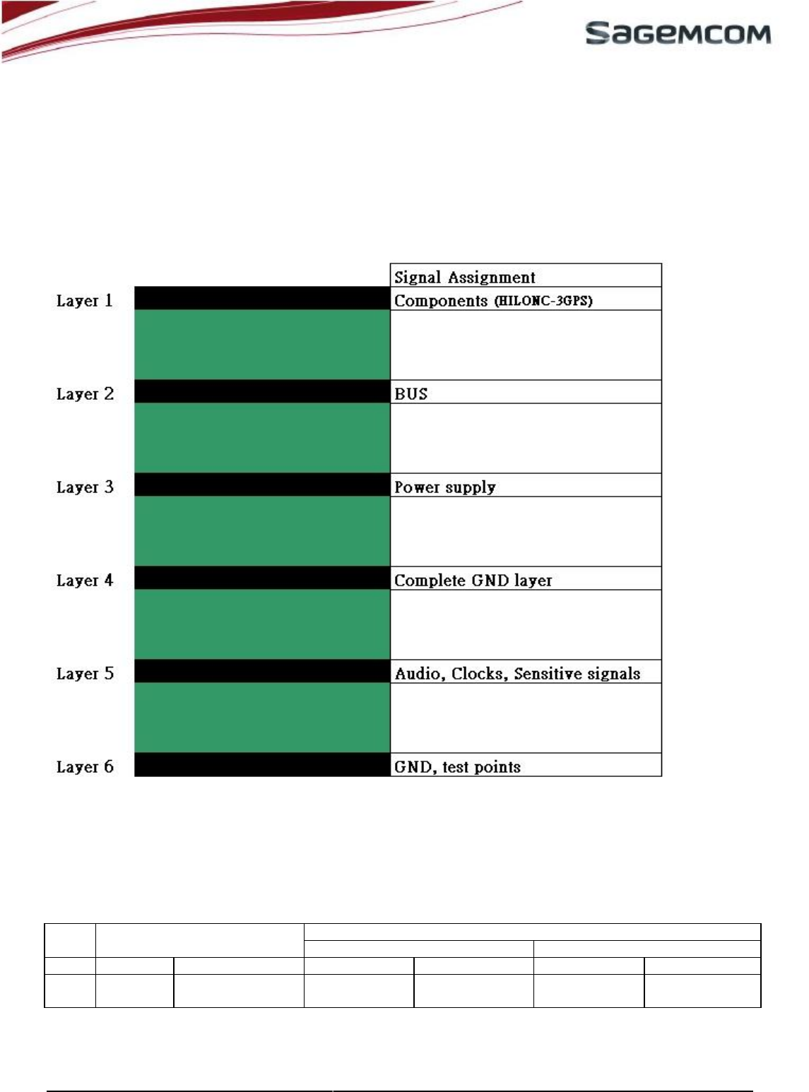
URD1
– OTL 5696.1–
022
/ 72740 Edition 0.4
HILONC-
3GPS
APPLICATION
NOTE
corresponding pins.
· Metalized plastic is not as effective as metal cans.
·
Shielded
inductors
might
be
needed
on
the
DC/DC
circuits,
or
they
might
need
to
be
placed
in
their
own
shield
area.
8.2.
Example
of
a
customer
board
layout
The following figure is an example of layer allocation for a 6-layer circuit (for reference purposes only):
Depending on the design the layout could also be done using 4 layers.
: 6 layer PCB stack
9.
Moisture
sensitivity
level
precautions
According to IPC/JEDEC J-STD 20, the HiLoNC 3GPS has the following MSL level: 3
Customer modules are shipped under a Dry package with all the MSL information labelled.
It
means
that
the
factory
must
process
and
solder
the
HiLoNC
3GPS
on
the
board
up
to
168
hours
(7
days)
after
the
HiLoNC
3GPS
sealed
package
have
been
opened.
This
duration
is
given
for
factory
floor conditions of T°<30°C, HR 60%.
Note d’étude / Technical document :
01/08/20111
-
Page
30
/
41
Level
Floor
Life
Soak
requirements
Standard
Accelerated
Equivalent
Time
Conditions
Time (hours)
Conditions
Time (hours)
Conditions
3
168
hours
<= 30°C/60% RH
192 +5/-0
30°C / 60% RH
40 +1/-0
60°C / 60%RH
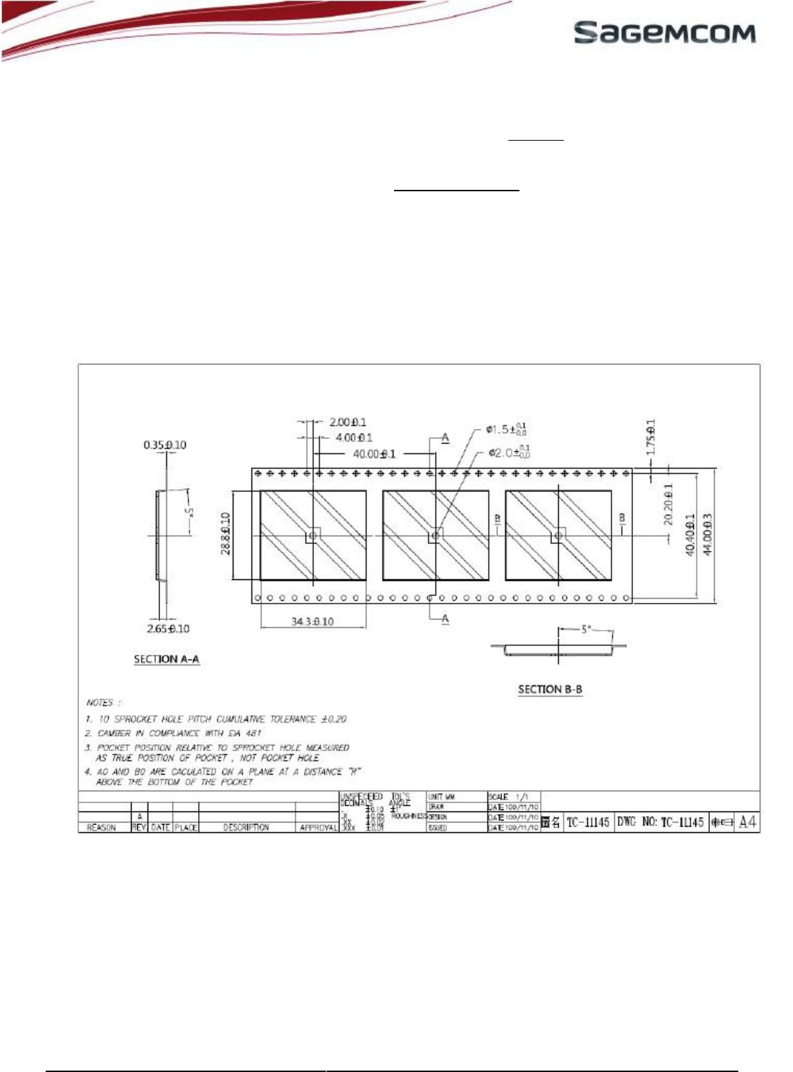
URD1
– OTL 5696.1–
022
/ 72740 Edition 0.4
HILONC-
3GPS
APPLICATION
NOTE
If this maximum 7 days duration can not be fulfilled, the HiLoNC 3GPS part must be baked again.
Unless
the
factory
floor
conditions
are
perfectly
controlled,
SAGEMCOM
does not
recommend
to
wait
until this maximum 7 days duration before soldering the HiLoNC 3GPS on board.
For
any
module
exposed
to
ambient
moisture
it
is
therefore
highly recommended
to
proceed
to
a
baking
according to the JEDEC (125°C during 24H) to dry the module before any soldering process
10
CUSTOMER
PROCESS
10.1
PACKAGE
The HILONC-3GPS module is delivered in Tape and Reel package which is hermetically sealed to prevent
from moisture and ESD.
The characteristics of the T&R are given in the drawing below.
Note d’étude / Technical document :
01/08/20111
-
Page
31
/
41
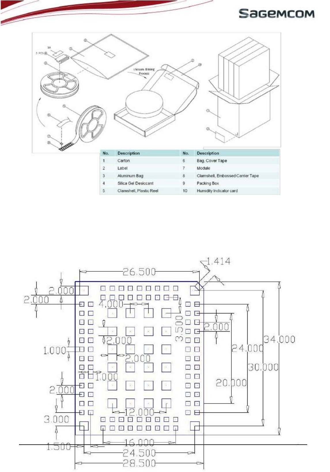
URD1
– OTL 5696.1–
022
/ 72740 Edition 0.4
HILONC-
3GPS
APPLICATION
NOTE
10.2
Stencil
Below are given soldering characteristics to report the HILONC-3GPS on the board.
10.2.1
Fotprint
Notes: all dimensions are in millimeter.
Note d’étude / Technical document :
01/08/20111
-
Page
32
/
41
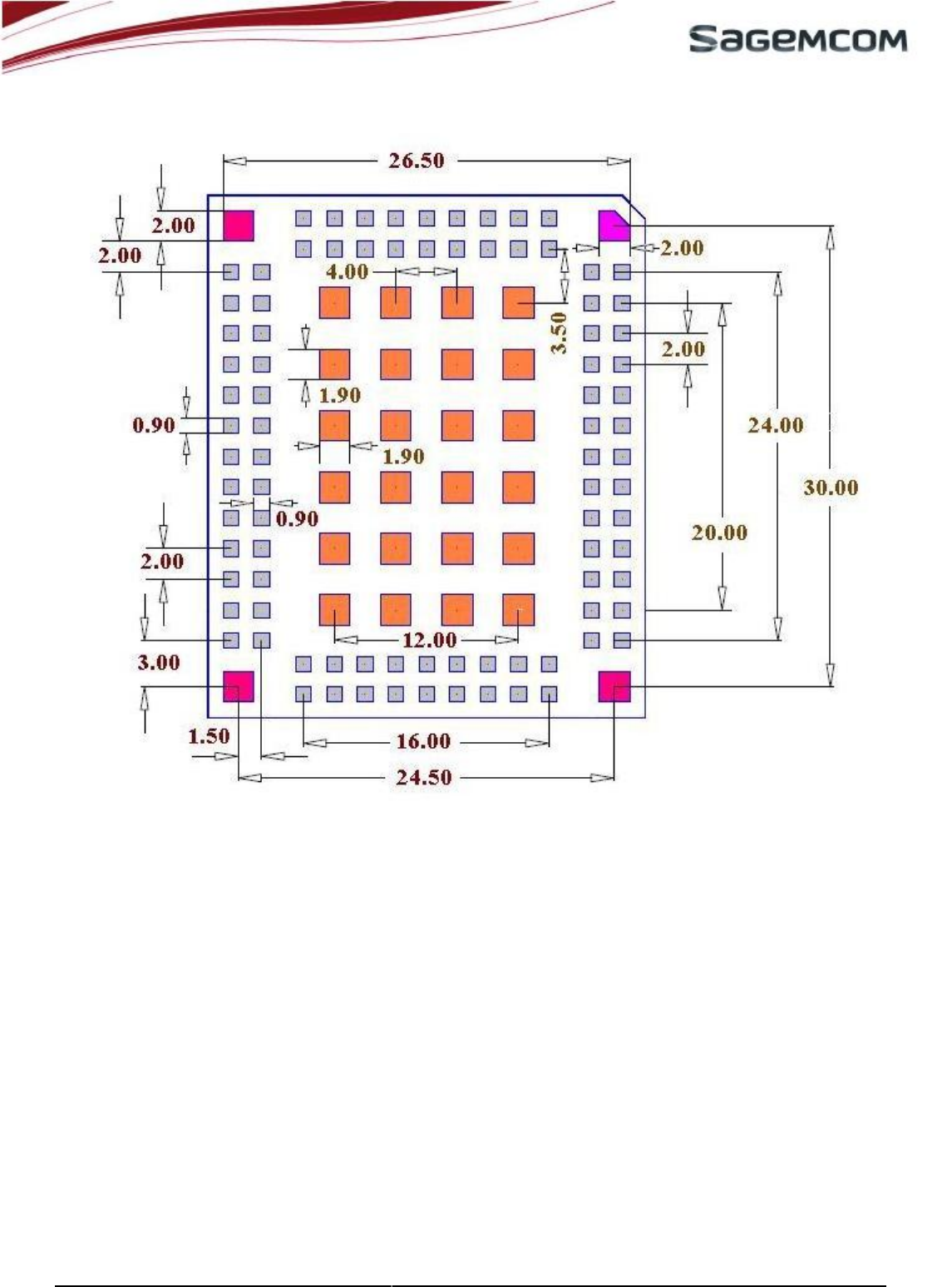
URD1
– OTL 5696.1–
022
/ 72740 Edition 0.4
HILONC-
3GPS
APPLICATION
NOTE
10.2.2
Recommended
Stencil
design
Stencil design advise thickness : 0.08mm ~ 0.13mm.
Solder paste advise thickness : 0.10mm ~ 0.18mm
10.3
Solder
Paste
SAGEMCOM
recommends
Use of "No Clean" ASAHI soldering paste is strongly recommended, as it does not
require cleaning after the soldering process has taken place. The paste listed in the example below
meets these criteria.
Solder paste: ACS-SN100C-MA1-S4 (Asahi Chemical (S) Pte Ltd.)
Alloy composition: Sn-0.7Cu-0.05Ni+Ge (99.2% Tin / 0.7 % Copper / 0.05% Nickel / Germanium)
Melting temperature: solidus 227°C / Peak 250°C / liquidus 227°C
10.4
Profile
for
Reflow
soldering
A convection type soldering oven is recommended.
Typical
usable
profile
is
shown
on
the
next
figure.
The
final
profile
has
to
be
tuned
depending
on
other
elements
like solder paste, board, other
Peak temperature: 235~250 Degree C.
Reflow zone (Above 220 Degree C): 30~70 sec.
Preheat zone (140~190 Degree C.): 60~120 sec.
Average ramp up rate : 2~4°C/second
Note d’étude / Technical document :
01/08/20111
-
Page
33
/
41
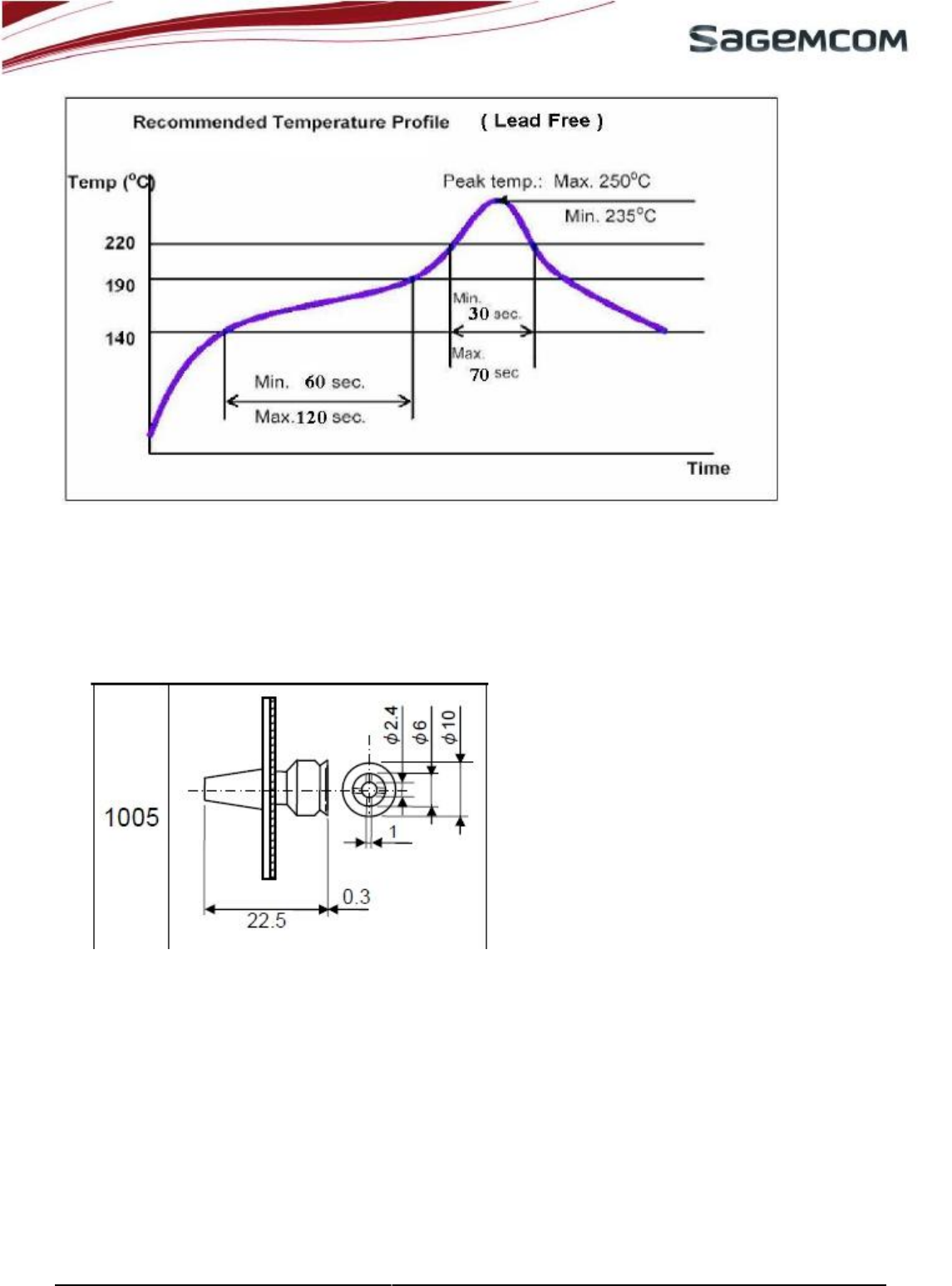
URD1
– OTL 5696.1–
022
/ 72740 Edition 0.4
HILONC-
3GPS
APPLICATION
NOTE
10.5
SMT
Machine
10.5.1
Nozzles
SAGEMCOM recommends using SMT machine with nozzle diameters up to 10 mm in order to always have
best prehension of the HILONC-3GPS module.
SAGEMCOM recommends using the following references of nozzles:
For the Panasonic, the nozzle 1005
10.5.2
Fiducials
There is no fiducials design on the bottom side of the HILONC-3GPS.
10.6
Underfill
The HILONC-3GPS shield did not be designed accordingly to allow this underfill process.
10.7
Second
reflow
soldering
Even if SAGEMCOM recommends a single reflow soldering, a second reflow soldering can be conceivable.
Positive tests have been performed with HILONC-3GPS on the bottom side.
Note d’étude / Technical document :
01/08/20111
-
Page
34
/
41
URD1
– OTL 5696.1–
022
/ 72740 Edition 0.4
HILONC-
3GPS
APPLICATION
NOTE
10.8
Hand
soldering
Hand soldering is impossible for HILONC-3GPS.
10.9
Unsoldering
Manual unsoldering is possible, for repair purpose for example.
A special care must be considered in order to avoid overheating the HILONC-3GPS.
For repairing: Usage of hot plate like example below can be considered with additional metallic cubic plate
whose dimensions are HILONC-3GPS's ones (to heat only HILONC-3GPS surface)
Customer must remember to not have components on the HILONC-3GPS opposite side of the
board.
11.
Labelling
The
HILONC-3GPS
module
is
labeled
with
its
own
FCC
ID
(XXXHILONC-3GPS)
on
the
shield
side.
When
the
module
is
installed
inside
product,
the
FCC
ID
label
on
the
module
will
not
be
visible.
To
avoid
this
scenario
an
exterior
label
must
be
stuck
on
the
surface
of
the
product
to
indicate
the
FCC
ID
of
the
enclosed
module.
The
label
can
use
the
following
wording:
transmitter
module
FCC
ID:
XXXHILONC-
3GPS or FCC ID: XXXHILONC-3GPS
12.
CE/FCC/IC
warning
statement
Europe
–
EU
Declaration
of
Conformity
This device complies with the essential requirements of the R&TTE Directive 1999/5/EC. The following test
methods
have
been
applied
in
order
to
prove
presumption
of
conformity
with
the
essential
requirements
of
the
R&TTE Directive 1999/5/EC:
- EN 60950-1: 2006+A11:2009:+A1:2010+A12:2011
Safety of Information Technology Equipment
- EN 301 908-2 V5.2.1
- EN 62311: 2008
Assessment of electronic and electrical equipment related to human exposure restrictions for
electromagnetic fields (0 Hz-300 GHz)
(IEC 62311:2007 (Modified))
- EN 301 908-1 V4.2.1
-
Electromagnetic
compatibility
and
Radio
spectrum
Matters
(ERM);
Base
Stations
(BS),
Repeaters
and
User
Equipment
(UE)
for
IMT-2000
Third-Generation
cellular
networks;
Part
1:
Harmonized
EN
for
IMT-2000,
introduction and common requirements, covering essential requirements of article 3.2 of the R&TTE
Directive
- EN 301 511 V9.0.2: 2003
Note d’étude / Technical document :
01/08/20111
-
Page
35
/
41

URD1
– OTL 5696.1–
022
/ 72740 Edition 0.4
HILONC-
3GPS
APPLICATION
NOTE
-
Global
System
for
Mobile
communications
(GSM);
Harmonized
standard
for
mobile
stations
in
the
GSM
900
and
DCS
1800
bands
covering
essential
requirements
under
article
3.2
of
the
R&TTE
directive
(1999/5/EC)
EN 301 489-1 V1.8.1: 2008
Electromagnetic compatibility and Radio Spectrum Matters (ERM); ElectroMagnetic Compatibility (EMC)
standard for radio equipment and services; Part 1: Common technical requirements
EN 301 489-7 V1.3.1: 2005
ElectroMagnetic compatibility and Radio spectrum Matters (ERM); ElectroMagnetic Compatibility (EMC)
standard for radio equipment ad services; Part 7: Specific conditions for mobile and portable radio and
ancillary equipment of digital cellular radio telecommunications systems (GSM and DCS)
EN 301 489-24 V1.5.1: 2010
Electromagnetic compatibility and Radio Spectrum Matters (ERM); ElectroMagnetic Compatibility (EMC)
standard for radio equipment and services; Part 24: Specific conditions for IMT-2000 CDMA Direct Spread
(UTRA) for Mobile and portable (UE) radio and ancillary equipment
EN 301 489-3 V1.4.1
0682
Note d’étude / Technical document :
01/08/20111
-
Page
36
/
41
[Czech]
[Jméno
výrobce]
tímto
tento
[typ
zařízení]
je
ve
se
základními
a
ustanoveními
1999/5/ES.
Dansk
[Danish]
Undertegnede
[fabrikantens
navn]
erklærer
herved,
at
følgende
udstyr
[udstyrets
typebetegnelse]
overholder
de
væsentlige
krav
og
øvrige
relevante
krav
i
direktiv
1999/5/EF.
Deutsch
[German]
Hiermit
erklärt
[Name
des
Herstellers],
dass
sich
das
Gerät
[Gerätetyp]
in
Übereinstimmung
mit
den
grundlegenden
Anforderungen
und
den
übrigen
einschlägigen
Bestimmungen
der
Richtlinie
1999/5/EG
befindet.
Eesti
[Estonian]
Käesolevaga
kinnitab
[tootja
nimi
=
name
of
manufacturer]
seadme
[seadme
tüüp
=
type
of
equipment]
vastavust
direktiivi
1999/5/EÜ
põhinõuetele
ja
nimetatud
direktiivist
tulenevatele
teistele
asjakohastele
sätetele.
English
Hereby,
[name
of
manufacturer],
declares
that
this
[type
of
equipment]
is
in
compliance
with
the
essential
requirements
and
other
relevant
provisions
of
Directive
1999/5/EC.
Español
[Spanish]
Por
medio
de
la
presente
[nombre
del
fabricante]
declara
que
el
[clase
de
equipo]
cumple
con
los
requisitos
esenciales
y
cualesquiera
otras
disposiciones
aplicables
o
exigibles
de
la
Directiva
1999/5/CE.
[Greek]
[name
of
manufacturer]
[type
of
equipment]
Français
[French]
Par
la
présente
[nom
du
fabricant]
déclare
que
l'appareil
[type
d'appareil]
est
conforme
aux
exigences
essentielles
et
aux
autres
dispositions
pertinentes
de
la
directive
1999/5/CE.
Italiano
[Italian]
Con
la
presente
[nome
del
costruttore]
dichiara
che
questo
[tipo
di
apparecchio]
è
conforme
ai
requisiti
essenziali
ed
alle
altre
disposizioni
pertinenti
stabilite
dalla
direttiva
1999/5/CE.
Latviski
[Latvian]
Ar
[name
of
manufacturer
/
izgatavotāja
nosaukums]
ka
[type
of
equipment
/
iekārtas
tips]
atbilst
1999/5/EK
un
citiem
ar
to
noteikumiem.
[Lithuanian]
[manufacturer
name]
deklaruoja,
kad
s
[equipment
type]
atitinka
esminius
reikalavimus
ir
kitas
1999/5/EB
Direktyvos
nuostatas.
Nederlands
[Dutch]
Hierbij
verklaart
[naam
van
de
fabrikant]
dat
het
toestel
[type
van
toestel]
in
overeenstemming
is
met
de
essentiële
eisen
en
de
andere
relevante
bepalingen
van
richtlijn
1999/5/EG.
Malti
[Maltese]
Hawnhekk,
[isem
tal-manifattur],
jiddikjara
li
dan
[il-mudel
tal-prodott]
jikkonforma
mal-
essenzjali
u
ma
provvedimenti
relevanti
li
hemm
fid-Dirrettiva
1999/5/EC.
Magyar
[Hungarian]
Alulírott,
[gyártó
neve]
nyilatkozom,
hogy
a
[...
típus]
megfelel
a
vonatkozó
alapvetõ
követelményeknek
és
az
1999/5/EC
irányelv
egyéb
elõírásainak.

URD1
– OTL 5696.1–
022
/ 72740 Edition 0.4
HILONC-
3GPS
APPLICATION
NOTE
Federal
Communication
Commission
Interference
Statement
This device complies with Part 15 of the FCC Rules. Operation is subject to the following two conditions: (1)
This device may not cause harmful interference, and (2) this device must accept any interference received,
including interference that may cause undesired operation.
This
equipment
has
been
tested
and
found
to
comply
with
the
limits
for
a
Class
B
digital
device,
pursuant
to
Part
15
of
the
FCC
Rules.
These
limits
are
designed
to
provide
reasonable
protection
against
harmful
interference
in
a
residential
installation.
This
equipment
generates,
uses
and
can
radiate
radio
frequency
energy
and,
if
not
installed
and
used
in
accordance
with
the
instructions,
may
cause
harmful
interference
to
radio
communications.
However,
there
is
no
guarantee
that
interference
will
not
occur
in
a
particular
installation.
If
this
equipment
does
cause
harmful
interference
to
radio
or
television
reception,
which
can
be
determined
by
turning
the
equipment
off and on, the user is encouraged to try to correct the interference by one of the following measures:
- Reorient or relocate the receiving antenna.
- Increase the separation between the equipment and receiver.
- Connect the equipment into an outlet on a circuit different from that
to which the receiver is connected.
-Consult the dealer or an experienced radio/TV technician for help.
FCC
Caution:
Any
changes
or
modifications
not
expressly
approved
by
the
party
responsible
for
compliance
could void the user's authority to operate this equipment.
This transmitter must not be co-located or operating in conjunction with any other antenna or transmitter.
This
device
complies
with
FCC
radiation
exposure
limits
set
forth
for
an
uncontrolled
environment.
In
order
to
avoid
the
possibility
of
exceeding
the
FCC
radio
frequency
exposure
limits,
human
proximity
to
the
antenna
shall not be less than 20cm (8 inches) during normal operation.
Note d’étude / Technical document :
01/08/20111
-
Page
37
/
41
Polski
[Polish]
Niniejszym [nazwa producenta] [nazwa wyrobu] jest zgodny z zasadniczymi
wymogami oraz stosownymi postanowieniami Dyrektywy 1999/5/EC.
Português
[Portuguese]
[Nome do fabricante] declara que este [tipo de equipamento] está conforme com os requisitos
essenciais e outras disposições da Directiva 1999/5/CE.
Slovensko
[Slovenian]
[Ime proizvajalca] izjavlja, da je ta [tip opreme] v skladu z bistvenimi zahtevami in ostalimi
relevantnimi i direktive 1999/5/ES.
Slovensky
[Slovak]
[Meno výrobcu] týmto vyhlasuje, [typ zariadenia] základné a
ustanovenia Smernice 1999/5/ES.
Suomi
[Finnish]
[Valmistaja = manufacturer] vakuuttaa täten että [type of equipment = laitteen tyyppimerkintä]
tyyppinen laite on direktiivin 1999/5/EY oleellisten vaatimusten ja sitä koskevien direktiivin
muiden ehtojen mukainen.
Svenska
[Swedish]
Härmed intygar [företag] att denna [utrustningstyp] står I överensstämmelse med de väsentliga
egenskapskrav och övriga relevanta bestämmelser som framgår av direktiv 1999/5/EG.

URD1
– OTL 5696.1–
022
/ 72740 Edition 0.4
HILONC-
3GPS
APPLICATION
NOTE
Industry
Canada
statement:
This device complies with RSS-210 of the Industry Canada Rules. Operation is subject to the following two
conditions:
(1)
This
device
may
not
cause
harmful
interference,
and
(2)
this
device
must
accept
any
interference
received, including interference that may cause undesired operation.
Ce
dispositif
est
conforme
à
la
norme
CNR-210
d'Industrie
Canada
applicable
aux
appareils
radio
exempts
de
licence.
Son
fonctionnement
est
sujet
aux
deux
conditions
suivantes:
(1)
le
dispositif
ne
doit
pas
produire
de
brouillage
préjudiciable,
et
(2)
ce
dispositif
doit
accepter
tout
brouillage
reçu,
y
compris
un
brouillage
susceptible
de provoquer un fonctionnement indésirable.
Radiation
Exposure
Statement:
This
equipment
complies
with
IC
radiation
exposure
limits
set
forth
for
an
uncontrolled
environment.
This
equipment
should
be
installed
and
operated
with
minimum
distance
20cm
between
the
radiator
&
your
body.
Declaration
d'exposition
aux
radiations:
Cet
equipement
est
conforme
aux
limites
d'exposition
aux
rayonnements
IC
etablies
pour
un
environnement
non
controle.
Cet
equipement
doit
etre
installe
et
utilise
avec
un
minimum
de
20
cm
de
distance
entre
la
source de rayonnement et votre corps.
This
device
is
intended
only
for
OEM
integrators
under
the
following
conditions:
1) The antenna must be installed such that 20 cm is maintained between the antenna and
users, and
2) The transmitter module may not be co-located with any other transmitter or antenna.
As long as 2 conditions above are met, further transmitter test will not be required. However, the OEM
integrator is still responsible for testing their end-product for any additional compliance requirements
required with this module installed
Cet
appareil
est
conçu
uniquement
pour
les
intégrateurs
OEM
dans
les
conditions
suivantes:
(Pour
utilisation
de
dispositif
module)
1) L'antenne doit être installée de telle sorte qu'une distance de 20 cm est respectée entre l'antenne
et les utilisateurs, et
2) Le module émetteur peut ne pas être coïmplanté avec un autre émetteur ou antenne.
Tant que les 2 conditions ci-dessus sont remplies, des essais supplémentaires sur l'émetteur ne seront pas
nécessaires. Toutefois, l'intégrateur OEM est toujours responsable des essais sur son produit final pour
toutes exigences de conformité supplémentaires requis pour ce module installé.
IMPORTANT
NOTE:
In the event that these conditions can not be met (for example certain laptop
configurations or co-location with another transmitter), then the FCC/Canada authorization is no longer
considered valid and the FCC/IC ID can not be used on the final product. In these circumstances, the
OEM integrator will be responsible for re-evaluating the end product (including the transmitter) and
obtaining a separate FCC/Canada authorization.
NOTE
IMPORTANTE:
Dans le cas où ces conditions ne peuvent être satisfaites (par exemple pour certaines configurations
d'ordinateur portable ou de certaines co-localisation avec un autre émetteur), l'autorisation du Canada
n'est plus considéré comme valide et l'ID IC ne peut pas être utilisé sur le produit final. Dans ces
circonstances, l'intégrateur OEM sera chargé de réévaluer le produit final (y compris l'émetteur) et
l'obtention d'une autorisation distincte au Canada.
Note d’étude / Technical document :
01/08/20111
-
Page
38
/
41

URD1
– OTL 5696.1–
022
/ 72740 Edition 0.4
HILONC-
3GPS
APPLICATION
NOTE
End
Product
Labeling
This transmitter module is authorized only for use in device where the antenna may be installed such that
20 cm may be maintained between the antenna and users. The final end product must be labeled in a
visible area with the following: FCC ID: VW3HILONC-3GPS
Contains IC: 9140A-HILONC-3GPS
The grantee's FCC ID/IC ID can be used only when all FCC/Canada compliance requirements are met.
Plaque
signalétique
du
produit
final
Ce
module
émetteur
est
autorisé
uniquement
pour
une
utilisation
dans
un
dispositif
où
l'antenne
peut
être
installée
de
telle
sorte
qu'une
distance
de
20cm
peut
être
maintenue
entre
l'antenne
et
les
utilisateurs.
Le
produit
final
doit
être
étiqueté
dans
un
endroit
visible
avec
l'inscription
suivante:
"Contient
des
IC:
9140A-
HILONC-3GPS".
Manual
Information
To
the
End
User
The OEM integrator has to be aware not to provide information to the end user regarding how to install or
remove this RF module in the manual of the end product which integrates this module.
The end user manual shall include all required regulatory information/warning as show in this manual.
Manuel
d'information
à
l'utilisateur
final
L'intégrateur
OEM
doit
être
conscient
de
ne
pas
fournir
des
informations
à
l'utilisateur
final
quant
à
la
façon
d'installer
ou
de
supprimer
ce
module
RF
dans
le
manuel
de
l'utilisateur
du
produit
final
qui
intègre
ce
module.
Le
manuel
de
l'utilisateur
final
doit
inclure
toutes
les
informations
réglementaires
requises
et
avertissements
comme indiqué dans ce manuel.
This device has been designed to operate with a dipole antenna have a maximum gain of [0.6] dB. Antenna
having
a
higher
gain
is
strictly
prohibited
per
regulations
of
Industry
Canada.
The
required
antenna
impedance
is 50 ohms.
Under Industry Canada regulations, this radio transmitter may only operate using an antenna of a type and
maximum (or lesser) gain approved for the transmitter by Industry Canada. To reduce potential radio
interference
to
other
users,
the
antenna
type
and
its
gain
should
be
so
chosen
that
the
equivalent
isotropically
radiated power (e.i.r.p.) is not more than that necessary for successful communication.
This
radio
transmitter
(IC:
9140A-HILONC-3GPS
/
Model:
HiLoNC-3GPS
)
has
been
approved
by
Industry
Canada
to
operate
with
the
antenna
type,
maximum
permissible
gain
and
required
antenna
impedance
for
each
antenna type indicated. Antenna types not included in this manual, having a gain greater than the
maximum gain indicated for that type, are strictly prohibited for use with this device.
Ce
dispositif
a
été
conçu
pour
fonctionner
avec
une
antenne
ayant
un
gain
maximal
de
dipole
antenne
avec
dB
[0.6]. Une antenne à gain plus élevé est strictement interdite par les règlements d'Industrie Canada.
L'impédance d'antenne requise est de 50 ohms.
Note d’étude / Technical document :
01/08/20111
-
Page
39
/
41

URD1
– OTL 5696.1–
022
/ 72740 Edition 0.4
HILONC-
3GPS
APPLICATION
NOTE
Conformément à la réglementation d'Industrie Canada, le présent émetteur radio peutfonctionner avec une
antenne
d'un
type
et
d'un
gain
maximal
(ou
inférieur)
approuvé
pourl'émetteur
par
Industrie
Canada.
Dans
le
but
de réduire les risques de brouillage radioélectriqueà l'intention des autres utilisateurs, il faut choisir le type
d'antenne et son gain de sorte que lapuissance isotrope rayonnée équivalente (p.i.r.e.) ne dépasse pas
l'intensité nécessaire àl'établissement d'une communication satisfaisante.
Le présent émetteur radio (IC: 9140A-HILONC-3GPS / Modèle: HiLoNC-3GPS ) a été approuvé par
Industrie
Canada
pour
fonctionner
avec
les
types
d'antenne
énumérés
ci-dessous
et
ayant
un
gain
admissible
maximal
et
l'impédance
requise
pour
chaque
type
d'antenne.
Les
types
d'antenne
non
inclus
dans
cette
liste,
ou
dont
le
gain
est
supérieur
au
gain
maximal
indiqué,
sont
strictement
interdits
pour
l'exploitation
de
l'émetteur.
Note d’étude / Technical document :
01/08/20111
-
Page
40
/
41

URD1
– OTL 5696.1–
022
/ 72740 Edition 0.4
HILONC-
3GPS
APPLICATION
NOTE
Declaration
of
Conformity
We,
Sagemcom
SAS
Address: 250 Route de l'Empereur, 92848 Rueil Malmaison Cedex France
Declare under our own responsibility that the product:
Model:
HiLoNC-3GPS
Intended
use:
Qual-Band
GSM/GPRS/EDGE
and
Dual-Band
WCDMA/HSDPA/HSUPA/HSPA+
Voice
and
Data
Module
Complies with the essential requirements of Article 3 of the R&TTE 1999/5/EC Directive, if used for its
in
tended use and that the following standards have been applied:
1.
Health
(Article
3.1(a)
of
the
R&TTE
Directive)
Applied Standard(s):
EN62311 :2008
2.
Safety
(Article
3.1(a)
of
the
R&TTE
Directive)
Applied Standard(s):
EN 60950-1:2006+A11:2009+A1:2010+A12:2011
3.
Electromagnetic
compatibility
(Article
3.1
(b)
of
the
R&TTE
Directive)
Applied Standard(s):
EN 301 489-1 V1.8.1/-3 V1.4.1/-7V1.3.1/-24V1.5.1
4.
Radio
frequency
spectrum
usage
(Article
3.2
of
the
R&TTE
Directive)
Applied Standard(s):
EN 300 440-1V1.6.1/EN 300 440-2 V1.4.1
EN 301 908-2 V5.2.1/EN 301 908-1V4.2.1
EN301 511 V 9.0.2
Note d’étude / Technical document :
01/08/20111
-
Page
41
/
41