SAGEMCOM BROANDS MO300QBM GSM/GPRS/EDGE Module User Manual
SAGEMCOM SAS GSM/GPRS/EDGE Module Users Manual
UserManual.wiki
>
SAGEMCOM BROANDS
>
MO300QBM User Manual
Users Manual
Navigation menu
Upload a User Manual
Namespaces
Wiki Guide
HTML
PDF
Info
Views
User Manual
Discussion / Help
Navigation

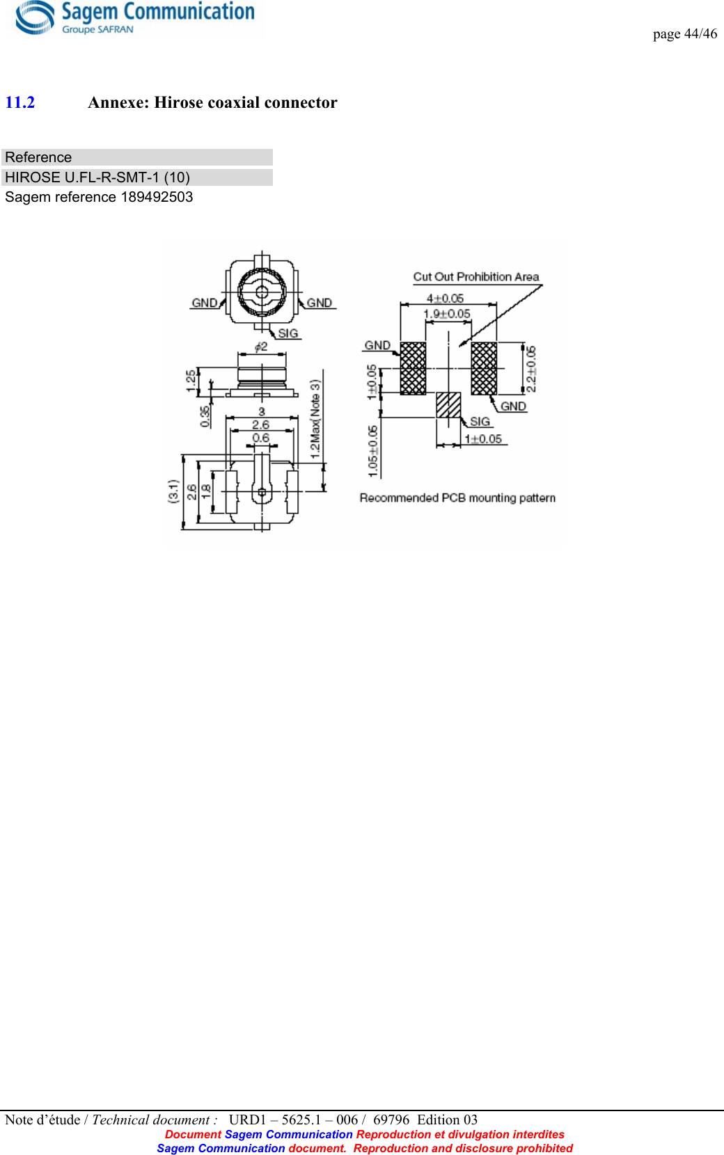
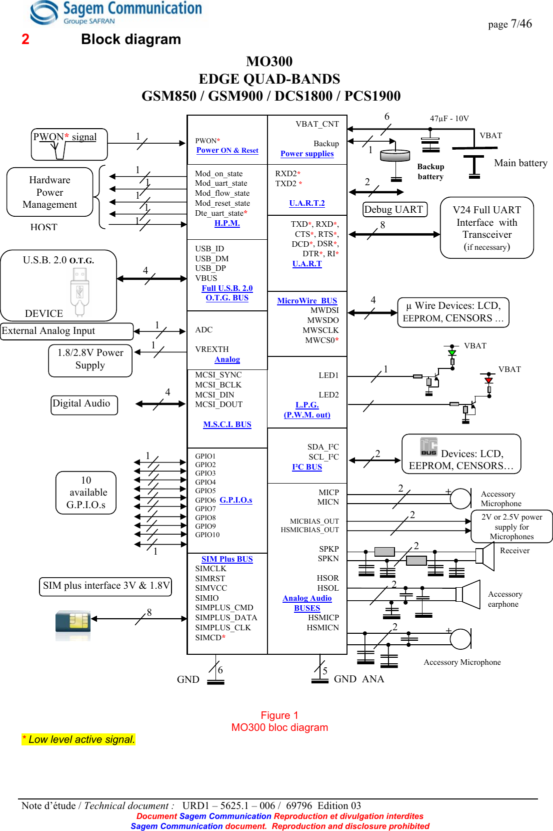
![page 6/46 Note d’étude / Technical document : URD1 – 5625.1 – 006 / 69796 Edition 03 Document Sagem Communication Reproduction et divulgation interdites Sagem Communication document. Reproduction and disclosure prohibited 1 Overview 1.1 Object of the document The aim of this document is to describe some examples of hardware solutions for developing some products around the SAGEM MO300 M2M Module. Most part of these solutions are not mandatory. Use them as suggestions of what should be done to have a working product and what should be avoided thanks to our experiences. This document suggests how to integrate the MO300 M2M module in wireless communicating devices such as GSM Gateway, POS, EDGE/GPS Tracking system, Wireless modem : connection with external devices, layout advises, external components (decoupling capacitors…). 1.2 Reference documents [ 1 ] URD1 – 5625.1 – 004 69772 - MO300 series modules specification [ 2 ] URD1 - 5625.1 - 014 69979 - AT Command Set for SAGEM Modules 1.3 Modification of this document The information presented in this document is supposed to be accurate and reliable. SAGEM assumes no responsibility for its use, nor any infringement of patents or other rights of third parties which may result from its use. This document is subject to change without notice. Changes or modifications not expressly approved by the party responsible for compliance could void the user's authority to operate the equipment. 1.4 FCC Compliance This device complies with Part 15 of the FCC Rules. Operation is subject to the following two conditions: 1. this device may not cause harmful interference, and 2. this device must accept any interference received; including interference that may cause undesired operation.](https://usermanual.wiki/SAGEMCOM-BROANDS/MO300QBM/User-Guide-1031835-Page-6.png)
![page 17/46 Note d’étude / Technical document : URD1 – 5625.1 – 006 / 69796 Edition 03 Document Sagem Communication Reproduction et divulgation interdites Sagem Communication document. Reproduction and disclosure prohibited 3.2.3 Using a mono Headset mode on the secondary audio path MO300 features a secondary audio path dedicated to be used with a Hands free kit accessory. This audio path can also be used instead of the main depending on the required audio power. An external microphone and earphone (32 ohms) can be connected to the MO300 Since the input unlink path is differential only mono headsets are supported, the speaker is connected between HSOR and HSOL. The microphone can be supplied using the internal MO300 bias supply (recommended but not mandatory) or any other external bias system compliant with selected microphone within the MO300 inputs limits. Figure 18 Mono audio headset Note: The capacitors have to be close to the external connector. 3.2.4 Audio interface selection In order to switch from one selection to the other, AT commands shall be used to configure the audio paths in case "SGV" file is used by default. Refer to relevant paragraph of document [ 2 ] to implement AT commands. 3.2.5 Multi Channel Serial Interface A MCSI bus is provided on the module MO300 for a digital interface application ( i.e. Bluetooth). Characteristics are the following : - Voice samples : 16bits, 8kHz - MCSI Clock : 520 kHz - Voltage : 1.8V More details can be given on request. 2.0V / 2.5V MICBIAS HSMICIP HSMICIN HSOR HSOL 22pF MO300 22pF 22pF 22pF22pF 22pF 1µF 100nF +1KΩ1KΩ](https://usermanual.wiki/SAGEMCOM-BROANDS/MO300QBM/User-Guide-1031835-Page-17.png)
![page 19/46 Note d’étude / Technical document : URD1 – 5625.1 – 006 / 69796 Edition 03 Document Sagem Communication Reproduction et divulgation interdites Sagem Communication document. Reproduction and disclosure prohibited If more than two LED are required, any GPIO can be used to drive a LED. A maximum of 10 GPIO are available on the MO300 Module. 3.3.1 Network LEDs connection. Green LED shall be connected to LED1, Red LED shall be connected to LED2, serial resistor shall be connected to each LED. These transistors can be found a in a single package referenced as UMDXX or PUMDXX Family. Value of resistor depends on characteristic of chosen LED, it is used to limit the current through the diode, Consider this formula to compute the resistor value in worst case: minmaxminminmax Id)Vcesat (Vd - Vbat R += Figure 19 Network LED connection 3.3.2 Network LEDs behaviour. As LEDs are driven through PWM outputs of the MO300, they can be configured with appropriate AT command. User application can set for each output : - Period between : 125ms and 3000ms - Time on between : 3,889 and 93,59 ms More details can be found in AT document referenced [ 2 ]. LED1 MO300 LED2 1 VBAT 1 VBAT RR](https://usermanual.wiki/SAGEMCOM-BROANDS/MO300QBM/User-Guide-1031835-Page-19.png)

![page 25/46 Note d’étude / Technical document : URD1 – 5625.1 – 006 / 69796 Edition 03 Document Sagem Communication Reproduction et divulgation interdites Sagem Communication document. Reproduction and disclosure prohibited 3.8.3 Backup Battery technology recommended 3.8.3.1 Manganese Silicon Lithium-Ion rechargeable Battery Sagem does not recommend to use this kind of technology because of the following drawbacks: • the maximum discharge current is limited (Shall be compliant with the module characteristics) • the over-discharge problem: most of the Lithium Ion rechargeable batteries are not able to recover their charge when their voltage reaches a low-level voltage. To avoid this, it is necessary to add a safety component to disconnect the backup battery in case of over–discharge condition. In such a case, this implementation is too complicated (too much components for that function). • The charging current has to be regulated SAGEM does not recommend to use this kind of backup battery technology at all. 3.8.3.2 Capacitor Battery These kinds of backup battery have not the drawbacks of the Lithium Ion rechargeable battery. As there are only capacitors: • the maximum discharge current is generally bigger, • there is no problem of over-discharge: the capacitor is able to recover its full charge even if its voltage has previously fallen to 0V. • there is no need to regulate the charging current. Moreover, this kind of battery is available in the same kind of package than the Lithium Ion cell and fully compatible on a mechanical point of view. The only disadvantage is that the capacity of this kind of battery is significantly smaller than Manganese Silicon Lithium Ion battery. But for this kind of use (supply internal RTC when the main battery is removed), the capacity is generally enough. SAGEM strongly recommends to use this kind of backup battery technology. 3.9 General Purpose Input Output Ten General Purpose Input Output (GPIO) are available on the board to board connector. The customer application can directly use them through the appropriate AT command as : - output : pin is set to High or Low state - input : pin is read on request and answer is given to the customer application. As input, different cases are possible to cover the maximum possible of customer application : - synchronous answer to the AT command (*) - Asynchronous answer to the AT command. The customer application previously to the request has configured the GPIO to react on falling/rising edges. The customer application is notified asynchronously by AT command answer when the configured trigger occurs. (*) : AT command process is not dedicated to real-time process. Then, driving the GPIO through this AT command is not aimed to emulated fast transient signals. All details to drive GPIO are given in AT commands document [ 2 ]. 3.10 Temperature sensor One temperature sensor is available on the MO300 module. Its is located on the MO300 PCB (near the board to board connector) and not under the MO300 shield in order to give the ambient temperature of the customer application. Due to the fast react and sensitivity of the temperature sensor, the result can be more or less accurate depending on possible draughts affecting the sensor. To give more precise results, the temperature sensor must be , as far as possible, isolated from draughts in the customer design. The temperature sensor covers all the operational temperature range of the MO300 module. The temperature can be read on request through appropriate AT commands as described in AT commands document [ 2 ].](https://usermanual.wiki/SAGEMCOM-BROANDS/MO300QBM/User-Guide-1031835-Page-25.png)
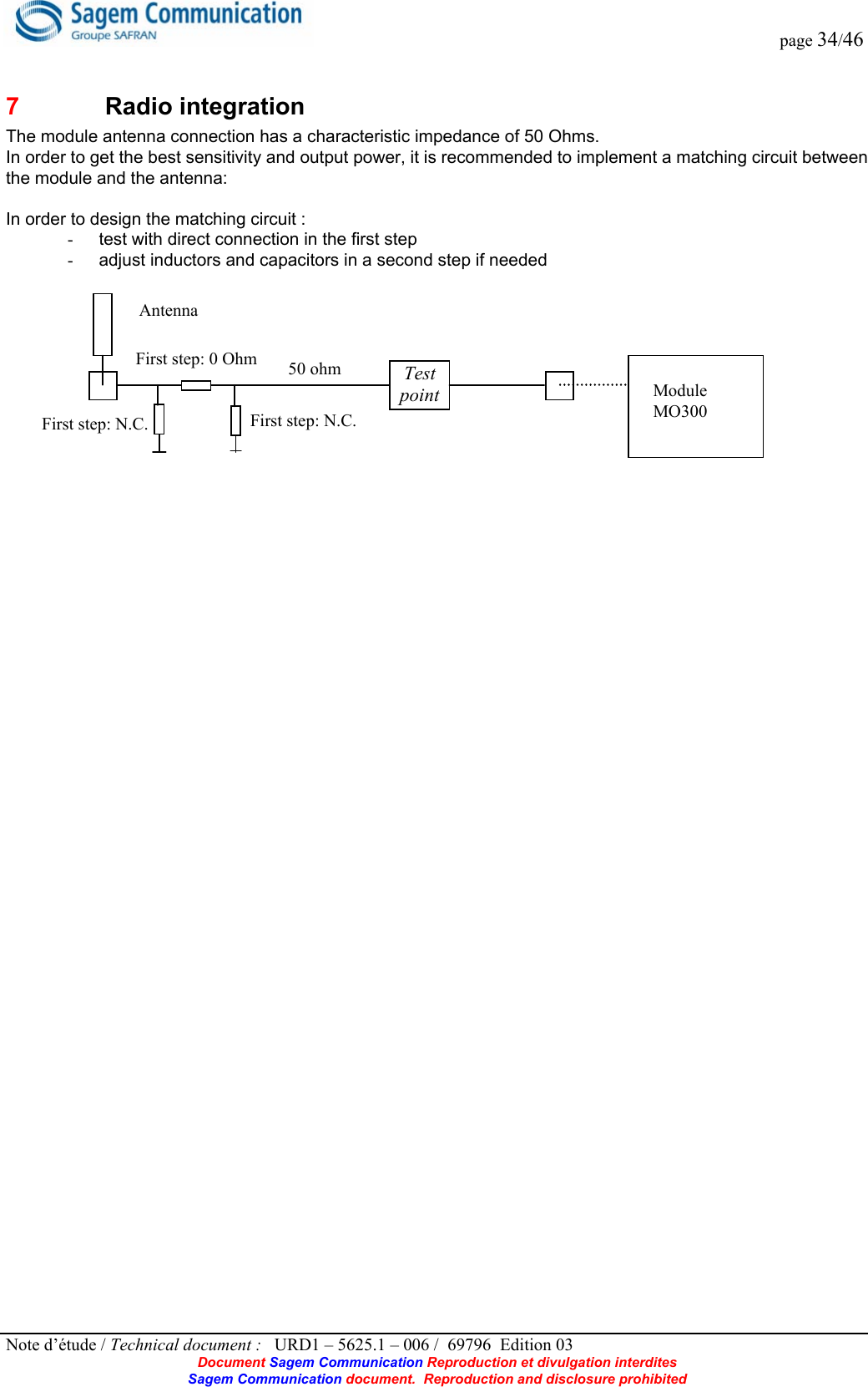
![page 26/46 Note d’étude / Technical document : URD1 – 5625.1 – 006 / 69796 Edition 03 Document Sagem Communication Reproduction et divulgation interdites Sagem Communication document. Reproduction and disclosure prohibited 3.11 ADC The ADC value can be read by the specific AT command as defined in the document referenced [2]. The input limits are the following: from 0V up to 1750mV The returned value is on 10 bits converted to decimal. 3.12 Micro-wire Bus The microwire bus is available but the client has to ask SAGEM to develop the driver and the specific application related the connected device. 3.13 Antenna detection Antenna detection can be provided if following criteria are met : • Antenna design is performed according to design given below. • Feature is activated through AT command. AT command answer can be synchronous or asynchronous depending on customer request, as described in AT command document referenced [ 2 ]. L MO300 Antenna contacts A coil L of 39µH must be added inside the antenna connector. Antenna Antenna connector 50Ω track](https://usermanual.wiki/SAGEMCOM-BROANDS/MO300QBM/User-Guide-1031835-Page-26.png)
![page 27/46 Note d’étude / Technical document : URD1 – 5625.1 – 006 / 69796 Edition 03 Document Sagem Communication Reproduction et divulgation interdites Sagem Communication document. Reproduction and disclosure prohibited 3.14 Hardware Power management and multiplexing interfaces In case hardware power management and multiplexing are used, it is necessary to isolate host and module MO300 in order to not generate current re-injection when MO300 is switched-off. Typical schematics (only useful signals are represented): Figure 26 Hardware interface between MO300 and host In a general case, solution 1 ( cheaper) is enough to protect the module MO300. 3.15 Resetting the module The MO300 module supports 2 kinds of reset: • External software reset activated by the AT command as defined in the document referenced [2] • External level 1 priority Hardware reset by pulling down the PWON* signal more than 8.2 seconds, on the next rise of PWON* the module is trigged. The reset is done 8.2 seconds later. This hardware reset, resets all the registers as well as the real time clock register, it is unconditional and have the highest priority. The module is in off mode after this hardware reset and need a new starting sequence to start again. At least 16.4 seconds are necessary to perform the hardware reset. 3.16 Starting the module There are two ways to start the MO300 module. 3.16.1 Use of PWON* First power up VBAT, which must be in the range 3.3V – 4.5V, and able to provide at least 2A during the TX bursts (refer to the module specification for more details). To start the module, a low level pulse must be sent on PWON* during more than 31.25ms (at 25°C). This duration increases as the temperature decreases (up to ~ 1 second at –30°C). After ~3 seconds CTS is active and so MOD_ON_STATE when it is ready to receive AT commands. To be sure that the pulse duration is enough to start the module, independently from the temperature, MOD_ON_STATE can be used as feedback to stop the pulse: DTR,RTS, RXD CTS, DSR, DCD, RI, TXD DTE_UART*_STATE, MOD_RESET_STATE, MOD_UART_STATE, MOD_FLOW_STATE, MOD_ON_STATE Tri-state command MO300HOST (PC)VREXTH Tri-state Buffers 100K Solution 1 Solution 2](https://usermanual.wiki/SAGEMCOM-BROANDS/MO300QBM/User-Guide-1031835-Page-27.png)
![page 29/46 Note d’étude / Technical document : URD1 – 5625.1 – 006 / 69796 Edition 03 Document Sagem Communication Reproduction et divulgation interdites Sagem Communication document. Reproduction and disclosure prohibited 3.17.2 Case of USB Interface As the module can also start when an USB cable is plugged, the sequence to stop the module needs the USB interface to be OFF or VBUS disconnected just after the command is sent and acknowledged by the module. Thus, to stop the module when the USB interface is used, use the AT command AT+CPOF, as defined in the document AT commands for MO300 series modules, then disconnect VBUS (unplug the USB cable or use a commanded switch to switch of VBUS) signal when the module acknowledges (responds OK) the command, otherwise the module restarts immediately (an OFF sequence is be performed followed by a power ON sequence). Figure 28 USB power command example 3.18 Sleep mode management The module can save power consumption when it's in sleep mode. The module switchs off the unused I/Os and LDOs to reduce the power consumption. When the module is in sleep mode the power consumption is reduced to it's minimum, the module stays in sleep mode and only wakes up to listen to the paging blocks (still able to receive calls). The module MO300 features 3 sleeps mode: The management is done using the AT command, as defined in the document AT referenced [2]. 3.18.1 First mode This mode allows the module to enter in sleep mode only when the DTE allows it. As long as the DTR signal is low, the module does not go into sleep mode. 3.18.2 Second mode This mode allows the module to decide to go into sleep mode by itself. 3.18.3 Third mode This mode allows the module to go into sleep mode according to the hardware power management specification using the 5 signals ( DTE_UART*_STATE, MOD_RESET_STATE, MOD_UART_STATE, MOD_FLOW_STATE, MOD_ON_STATE ). 3.18.4 USB connectivity impact on sleep mode When the USB interface is used, the MO300 module can not reach it's best power saving performances. The MO300 module can not go into sleep mode as long as USB interface is active. It is up to the Host responsibility to deactivate the USB connexion in order to allow sleep mode of the MO300 and then re-establish properly the USB connexion to communicate again with the MO300 module. USB ID VBUS MO300 (DEVICE) USB DP USB DM USB ID VBUS Command HOST USB DP USB DM](https://usermanual.wiki/SAGEMCOM-BROANDS/MO300QBM/User-Guide-1031835-Page-29.png)
![page 35/46 Note d’étude / Technical document : URD1 – 5625.1 – 006 / 69796 Edition 03 Document Sagem Communication Reproduction et divulgation interdites Sagem Communication document. Reproduction and disclosure prohibited 7.1 Antenna connection MO300 module feature two ways to connect it to the GSM antenna. 7.1.1 Mini Coaxial connector A mini-coaxial connector is provided on the MO300 : Hirose U.FL-R-SMT-1 (10) 7.1.2 Spring contacts • 50 Ω line matching (between module and MAIN board, and with RF test point) • SAGEM strongly recommends to solder the spring contact on the whole surface instead of only 2 points Keep matching circuit on MAIN board but with direct connection in the first step – it could be necessary to make some adjustment later, during RF qualification stage Figure 29 Spring contact mounting 7.2 Ground link area The MO300 feature 3 ground Pads for the RF. The 3 pads must be in contact with the ground plan of the main board. Otherwise the RF performances will be degraded. In case of need, if the 3 pads are not sufficient because of the client design, a metallic foam can be used as described here after. To have the best radio performances (spurious, sensitivity…),good ground contact between the module shielding and the main board is needed using for example 0.5 / 0.7mm metallic foam or label. Do not solder the shielding of the module on ground pad of the main board. Conductive foam: minimum size = 1cm x 3 cm (located on the top of MO300 shielding – near antenna area) minimal thickness = 0.5mm (take care of pressure % average) [20% compression] Figure 30 Metallic foam position To be avoided because of unwanted capacitors Good solution Bad solution Client MAIN board80 pins connector 0.5 to 0.7 mm At least 3 cm At least 1 cm Conductive foam for ground Position at the top MO300](https://usermanual.wiki/SAGEMCOM-BROANDS/MO300QBM/User-Guide-1031835-Page-35.png)