SAGEMCOM BROANDS MO300QBM GSM/GPRS/EDGE Module User Manual
SAGEMCOM SAS GSM/GPRS/EDGE Module Users Manual
Users Manual

page 1/46
Note d’étude / Technical document : URD1 – 5625.1 – 006 / 69796 Edition 03
Document Sagem Communication Reproduction et divulgation interdites
Sagem Communication document. Reproduction and disclosure prohibited
Direction des Recherches et des Développements Etablissement de VELIZY
VELIZY R&D Center
NOTE D'ETUDE / TECHNICAL DOCUMENT
TITRE / TITLE :
MO300 series module Application Note
RESUME / SUMMARY
This document is the application note for the MO300 series modules.
page 2/46
Note d’étude / Technical document : URD1 – 5625.1 – 006 / 69796 Edition 03
Document Sagem Communication Reproduction et divulgation interdites
Sagem Communication document. Reproduction and disclosure prohibited
Direction des Recherches et des Développements Etablissement de VELIZY
VELIZY R&D Center
NOTE D'ETUDE / TECHNICAL DOCUMENT
FICHE RECAPITULATIVE / SUMMARY SHEET
Ed Date
Date
Observations
Comments
1 24/08/2007 Création du document
/ Document creation
2 24/10/2007 Mise à jour / Major
update
3 13/10/2008 FCC Updates
4
5
6

page 3/46
Note d’étude / Technical document : URD1 – 5625.1 – 006 / 69796 Edition 03
Document Sagem Communication Reproduction et divulgation interdites
Sagem Communication document. Reproduction and disclosure prohibited
Direction des Recherches et des Développements Etablissement de VELIZY
VELIZY R&D Center
MO300 M2M MODULE
APPLICATION NOTE

page 4/46
Note d’étude / Technical document : URD1 – 5625.1 – 006 / 69796 Edition 03
Document Sagem Communication Reproduction et divulgation interdites
Sagem Communication document. Reproduction and disclosure prohibited
Direction des Recherches et des Développements Etablissement de VELIZY
VELIZY R&D Center
SOMMAIRE / CONTENTS
1 OVERVIEW ...................................................................................................................................................................6
1.1 OBJECT OF THE DOCUMENT .......................................................................................................................................6
1.2 REFERENCE DOCUMENTS...........................................................................................................................................6
1.3 MODIFICATION OF THIS DOCUMENT...........................................................................................................................6
1.4 FCC COMPLIANCE.....................................................................................................................................................6
2 BLOCK DIAGRAM.......................................................................................................................................................7
3 FUNCTIONAL INTEGRATION .................................................................................................................................8
3.1 HOW TO CONNECT A SIM CARD ?:.............................................................................................................................8
3.1.1 SIM on the Board to Board Connector.............................................................................................................9
3.1.1.1 Without SIM card detection ......................................................................................................................................... 10
3.1.1.2 With SIM card detection .............................................................................................................................................. 11
3.1.2 SIM holder soldered on the back of the MO300.............................................................................................12
3.1.2.1 Schematics.................................................................................................................................................................... 12
3.1.2.2 Placing.......................................................................................................................................................................... 13
3.2 HOW TO CONNECT THE AUDIOS? .........................................................................................................................14
3.2.1 Using a differential Handset mode on the main audio path...........................................................................14
3.2.1.1 Notes for microphone ................................................................................................................................................... 15
3.2.1.2 Notes for speaker.......................................................................................................................................................... 15
3.2.2 Non differential audio handset .......................................................................................................................16
3.2.3 Using a mono Headset mode on the secondary audio path............................................................................17
3.2.4 Audio interface selection ................................................................................................................................17
3.2.5 Multi Channel Serial Interface .......................................................................................................................17
3.2.6 Characteristics of the microphone and speaker recommended by SAGEM ...................................................18
3.2.6.1 Characteristics of the microphone recommended by SAGEM ..................................................................................... 18
3.2.6.2 Characteristics of the dual mode speaker recommended by SAGEM .......................................................................... 18
3.3 NETWORK LEDS.....................................................................................................................................................18
3.3.1 Network LEDs connection. .............................................................................................................................19
3.3.2 Network LEDs behaviour. ..............................................................................................................................19
3.4 POWER SUPPLY ........................................................................................................................................................20
3.5 V24 UART .............................................................................................................................................................20
3.5.1 Complete V24 – connection MO300 - host.....................................................................................................20
3.5.2 Complete V24 interface with PC ....................................................................................................................20
3.5.3 Partial V24 ( RX-TX-RTS-CTS) – connection MO300 - host .........................................................................21
3.5.4 Partial V24 ( RX-TX) – connection MO300 - host .........................................................................................22
3.6 UART 2 ..................................................................................................................................................................22
3.7 USB 2.0 OTG .........................................................................................................................................................22
3.8 BACKUP BATTERY ...................................................................................................................................................23
3.8.1 Backup battery function feature......................................................................................................................23
3.8.2 Current consumption on the backup battery ..................................................................................................24
3.8.2.1 Charge by internal MO300 charging function.............................................................................................................. 24
3.8.3 Backup Battery technology recommended......................................................................................................25
3.8.3.1 Manganese Silicon Lithium-Ion rechargeable Battery ................................................................................................. 25
3.8.3.2 Capacitor Battery.......................................................................................................................................................... 25
3.9 GENERAL PURPOSE INPUT OUTPUT .........................................................................................................................25
3.10 TEMPERATURE SENSOR............................................................................................................................................25
3.11 ADC........................................................................................................................................................................26
3.12 MICRO-WIRE BUS ....................................................................................................................................................26
3.13 ANTENNA DETECTION..............................................................................................................................................26
3.14 HARDWARE POWER MANAGEMENT AND MULTIPLEXING INTERFACES .....................................................................27
3.15 RESETTING THE MODULE .........................................................................................................................................27
3.16 STARTING THE MODULE...........................................................................................................................................27
3.16.1 Use of PWON*................................................................................................................................................27
3.16.2 Case of USB Plugged .....................................................................................................................................28

page 5/46
Note d’étude / Technical document : URD1 – 5625.1 – 006 / 69796 Edition 03
Document Sagem Communication Reproduction et divulgation interdites
Sagem Communication document. Reproduction and disclosure prohibited
3.17 STOPPING THE MODULE ...........................................................................................................................................28
3.17.1 Case of UART Interface..................................................................................................................................28
3.17.2 Case of USB Interface ....................................................................................................................................29
3.18 SLEEP MODE MANAGEMENT.....................................................................................................................................29
3.18.1 First mode.......................................................................................................................................................29
3.18.2 Second mode...................................................................................................................................................29
3.18.3 Third mode......................................................................................................................................................29
3.18.4 USB connectivity impact on sleep mode.........................................................................................................29
4 MANDATORY POINTS FOR THE FINAL TESTS AND TUNING .....................................................................30
5 ESD & EMC RECOMMENDATIONS......................................................................................................................31
5.1 STANDARD REQUIREMENTS FOR ESD......................................................................................................................31
5.1.1 ESD Analysis ..................................................................................................................................................31
5.1.2 Recommendations to avoid ESD issues ..........................................................................................................31
5.2 ESD FEATURES........................................................................................................................................................32
5.3 EMC RECOMMENDATIONS ......................................................................................................................................32
6 RECOMMENDED COMPONENTS .........................................................................................................................33
7 RADIO INTEGRATION.............................................................................................................................................34
7.1 ANTENNA CONNECTION...........................................................................................................................................35
7.1.1 Mini Coaxial connector ..................................................................................................................................35
7.1.2 Spring contacts ...............................................................................................................................................35
7.2 GROUND LINK AREA ................................................................................................................................................35
7.3 LAYOUT ..................................................................................................................................................................36
7.4 MECHANICAL SURROUNDING ..................................................................................................................................36
7.5 OTHER RECOMMENDATIONS – TESTS FOR PRODUCTION/DESIGN..............................................................................36
7.6 FCC RF COMPLIANCE .............................................................................................................................................36
8 AUDIO INTEGRATION.............................................................................................................................................37
8.1 MECHANICAL INTEGRATION AND ACOUSTICS .........................................................................................................37
8.2 ELECTRONICS AND LAYOUT.....................................................................................................................................37
9 RECOMMENDATIONS ON LAYOUT OF THE MAIN BOARD.........................................................................38
9.1 GENERAL RECOMMENDATIONS ON LAYOUT.............................................................................................................38
9.1.1 Ground............................................................................................................................................................38
9.1.2 Power supplies................................................................................................................................................38
9.1.3 Clocks .............................................................................................................................................................38
9.1.4 Data bus and other signals.............................................................................................................................38
9.1.5 Radio...............................................................................................................................................................38
9.1.6 Audio...............................................................................................................................................................38
9.2 EXAMPLE OF LAYOUT FOR MAIN BOARD ..................................................................................................................39
10 MECHANICAL INTEGRATION ..........................................................................................................................40
10.1 EXTERNAL CONNECTIONS PRESENTATION ...............................................................................................................40
10.2 CONNECTION CONSTRAINTS ....................................................................................................................................40
10.2.1 Board to board connection .............................................................................................................................40
10.2.2 Antenna connection ........................................................................................................................................41
10.3 WARNING RELATED TO THE USE OF METALLIC HOUSINGS........................................................................................41
11 SUMMARY OF INTEGRATION ..........................................................................................................................42
11.1 ANNEXE: MOLEX BOARD TO BOARD CONNECTOR...................................................................................................42
11.2 ANNEXE: HIROSE COAXIAL CONNECTOR .................................................................................................................44
11.3 ANNEXE: SPRING CONTACT FOR ANTENNA ..............................................................................................................45
12 LABEL.......................................................................................................................................................................46

page 6/46
Note d’étude / Technical document : URD1 – 5625.1 – 006 / 69796 Edition 03
Document Sagem Communication Reproduction et divulgation interdites
Sagem Communication document. Reproduction and disclosure prohibited
1 Overview
1.1 Object of the document
The aim of this document is to describe some examples of hardware solutions for developing some products
around the SAGEM MO300 M2M Module. Most part of these solutions are not mandatory. Use them as
suggestions of what should be done to have a working product and what should be avoided thanks to our
experiences.
This document suggests how to integrate the MO300 M2M module in wireless communicating devices such as
GSM Gateway, POS, EDGE/GPS Tracking system, Wireless modem : connection with external devices, layout
advises, external components (decoupling capacitors…).
1.2 Reference documents
[ 1 ] URD1 – 5625.1 – 004 69772 - MO300 series modules specification
[ 2 ] URD1 - 5625.1 - 014 69979 - AT Command Set for SAGEM Modules
1.3 Modification of this document
The information presented in this document is supposed to be accurate and reliable.
SAGEM assumes no responsibility for its use, nor any infringement of patents or other rights of third parties
which may result from its use.
This document is subject to change without notice.
Changes or modifications not expressly approved by the party responsible for compliance could void the user's
authority to operate the equipment.
1.4 FCC Compliance
This device complies with Part 15 of the FCC Rules. Operation is subject to the following two conditions:
1. this device may not cause harmful interference, and
2. this device must accept any interference received; including interference that may cause undesired
operation.
page 7/46
Note d’étude / Technical document : URD1 – 5625.1 – 006 / 69796 Edition 03
Document Sagem Communication Reproduction et divulgation interdites
Sagem Communication document. Reproduction and disclosure prohibited
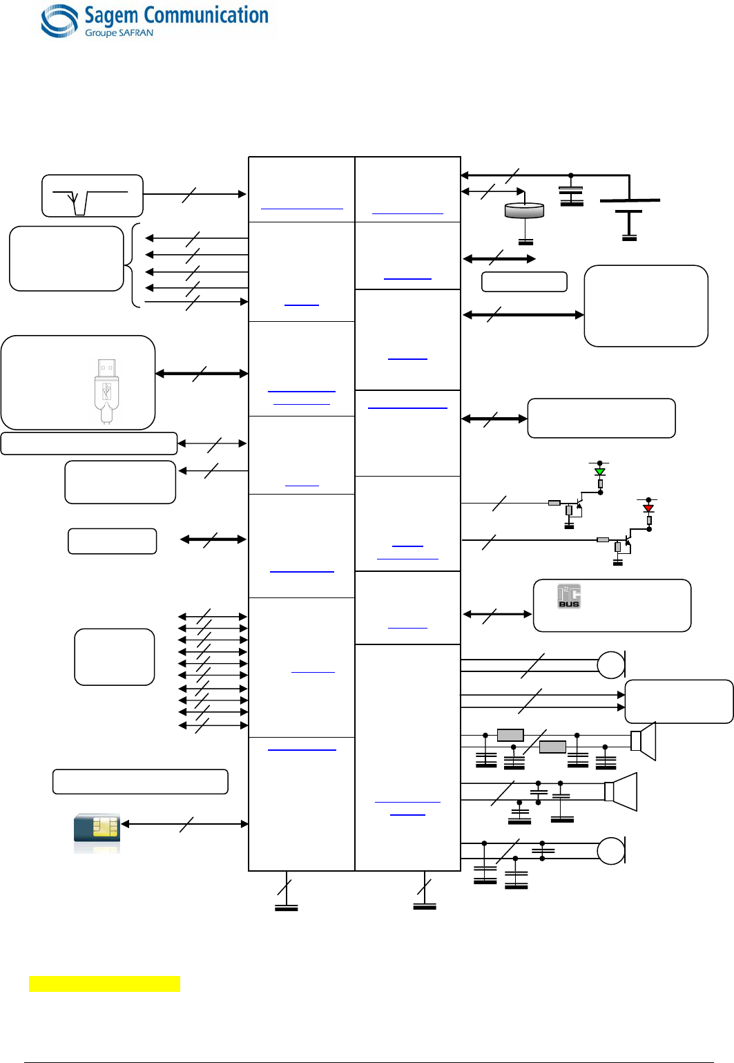
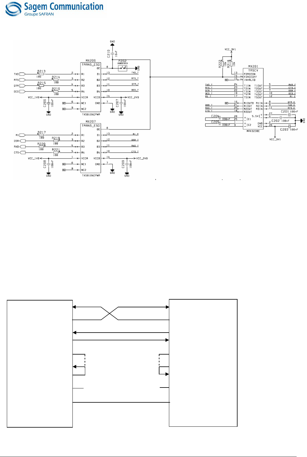
2 Block diagram
Figure 1
MO300 bloc diagram
* Low level active signal.
MO300
EDGE QUAD-BANDS
GSM850 / GSM900 / DCS1800 / PCS1900
Accessory Microphone
+
2
VBAT
Hardware
Power
Managemen
t
PWON*
Power ON & Reset
Mod_on_state
Mod_uart_state
Mod_flow_state
Mod_reset_state
Dte_uart_state*
H.P.M.
GPIO1
GPIO2
GPIO3
GPIO4
GPIO5
GPIO6 G.P.I.O.s
GPIO7
GPIO8
GPIO9
GPIO10
SIM Plus BUS
SIMCLK
SIMRST
SIMVCC
SIMIO
SIMPLUS_CMD
SIMPLUS_DATA
SIMPLUS_CLK
SIMCD*
MICP
MICN
MICBIAS_OUT
HSMICBIAS_OUT
SPKP
SPKN
HSOR
HSOL
Analog Audio
BUSES
HSMICP
HSMICN
SDA_I²C
SCL_I²C
I²C BUS
LED1
LED2
L.P.G.
(P.W.M. out)
ADC
VREXTH
Analog
MicroWire BUS
MWDSI
MWSDO
MWSCLK
MWCS0*
TXD*, RXD*,
CTS*, RTS*,
DCD*, DSR*,
DTR*, RI*
U.A.R.T
RXD2*
TXD2 *
U.A.R.T.2
VBAT_CNT
Backup
Power supplies
V24 Full UART
Interface with
Transceiver
(
if necessar
y
)
Accessory
earphone
Receiver
HOST
Accessory
Microphone
47
µ
F - 10V
6
1
2
8
4
1
2
GND ANA
GND
65
4
MCSI_SYNC
MCSI_BCLK
MCSI_DIN
MCSI_DOUT
M.S.C.I. BUS
2
2
2
2
VBAT
VBAT
1
1
SIM plus interface 3V & 1.8V
8
10
available
G.P.I.O.s
Digital Audio
1
1
USB_ID
USB_DM
USB_DP
VBUS
Full U.S.B. 2.0
O.T.G. BUS
1
1
1
1
µ Wire Devices: LCD,
EEPROM, CENSORS …
Backup
battery
Main battery
Debug UART
2V or 2.5V power
supply for
Micro
p
hones
PWON* signal
Devices: LCD,
EEPROM, CENSORS…
+
U.S.B. 2.0 O.T.G.
DEVICE
1.8/2.8V Power
Supply
1
1
4
External Analog Input
page 8/46
Note d’étude / Technical document : URD1 – 5625.1 – 006 / 69796 Edition 03
Document Sagem Communication Reproduction et divulgation interdites
Sagem Communication document. Reproduction and disclosure prohibited
3 Functional integration
The MO300 series modules target the M2M applications market.
Following the improvement of Silicon technologies includes functionality improvement, less power consumption,
low voltage and higher working frequencies clock, the MO300 module meets all these requirement and uses
last high end technology. All digital I/Os at the 80 pins connector are on 1.8V domain and 1.4 V for its core.
Except VREXTH (1.8V or 2.8V) and VCCSIM (and the SIM I/Os at 1.8V or 2.8V) and obviously VBAT.
Thus, all chip used to communicate with the MO300 must be compatible with this voltage requirement.
Otherwise you will be simply required to use level shifters to adapt the voltage of the signals to meet the
requirement of MO300 Module.
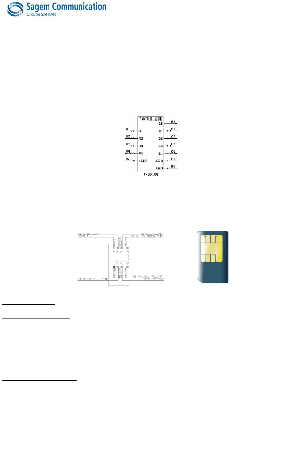
As example here is the validated chip on our design to shift I/Os voltage from 2.8V to 1.8V:
Figure 2
Example of Level Shifter
3.1 How to connect a SIM card ?:
Figure 3
Sim plus card
Preliminary notes:
Regarding the Sim cards:
Some improvements and new features are supported by new generation of Sim cards.
The main features are the support for 1.8 power supply for USIM used in EDGE, HSDPA and UMTS
applications.
The second one is the add-on, the flash memory included in Simplus card to mix and simplify the design of two
Card holder in some applications. If necessary, with only one mechanical card holder it is possible to have
access to Sim card features and at the same time to also have access to an external Flash memory module like
MMC.
Regarding the card holders:
The Sim card holder can have 6 or 8 pins depending if it feature a mechanical card presence detector or not.
The Simplus card holder can have 8 or 10 pins depending if it feature a card presence detector or not.
There are two ways to connect a Sim card holder to the MO300 module.
• External Sim card holder uses 10 pins if Simplus compliant or 8 pins if normal Sim compliant from Pin 5 to
pin 12 of the board to board (BtB)connector.
• Internal Sim card holder by soldering the card holder( and it's protective components) on the back side of
the MO300 module.
Note: These two ways are exclusives, never use both solutions at the same time. This is mandatory.
page 9/46
Note d’étude / Technical document : URD1 – 5625.1 – 006 / 69796 Edition 03
Document Sagem Communication Reproduction et divulgation interdites
Sagem Communication document. Reproduction and disclosure prohibited
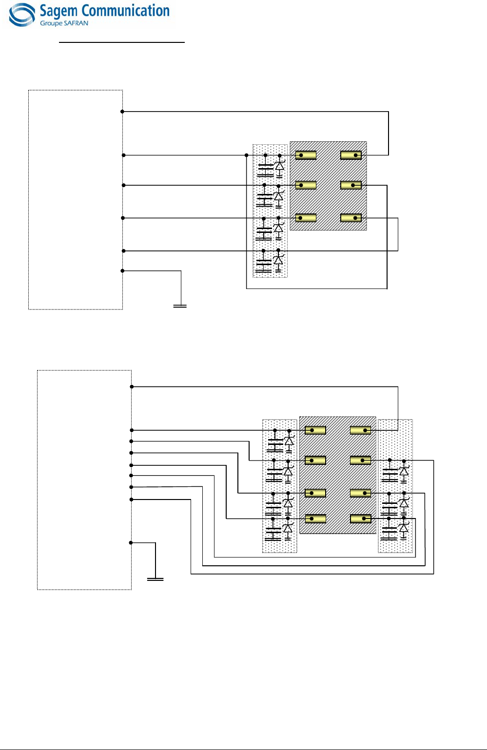
3.1.1 SIM on the Board to Board Connector.
The SIM card connection could be done in two ways:
• Connector with 6 pins without SIM card detection.
• Connector with 8 pins with SIM card detection.
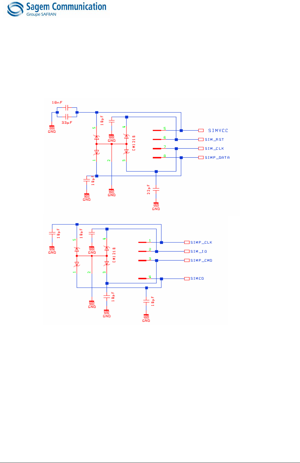
In both cases, decoupling capacitors of 10pF have to be added on SIMCLK, SIMRST, SIMVCC and SIMIO
signals as close as possible to the SIM card connector to avoid EMC issues. Moreover, use ESD protection
components to protect Sim card and module I/Os against Electro Static Discharges. The following schematic
show how to protect the Sim access for 8 pins connector. Apply the same method for a 6 pins connector.
Figure 4
Protections : EMC and ESD components close to the Sim
page 10/46
Note d’étude / Technical document : URD1 – 5625.1 – 006 / 69796 Edition 03
Document Sagem Communication Reproduction et divulgation interdites
Sagem Communication document. Reproduction and disclosure prohibited
3.1.1.1 Without SIM card detection
Normal SIM card case: 6 pins are used.
Figure 5
6 pins SIM card connection without presence detection
SIM Plus card case: 8 pins are used.
Figure 6
8 pins SIM plus card connection without presence detection
In these configurations, the SIMCD* signal is always Low.
There is no hardware SIM card detection, so the SIM card is considered as always present. (A software
detection is always performed). For filtering, EMC and ESD values refer to schematics figure 4.
GND
MO300
SIMVCC
SIMRST
SIMCLK
SIMIO
SIMCD*
VCC
RST
CLK I/O
VPP
GND
SIM connector
GND
MO300
SIMVCC
SIMRST
SIMCLK
SIMPLUS
_
DATA
SIMPLUS_CMD
SIMIO
SIMPLUS_CLK
SIMCD*
VCC
RST
I/O
SP CL
K
GND
SP DATA SP CMD
page 11/46
Note d’étude / Technical document : URD1 – 5625.1 – 006 / 69796 Edition 03
Document Sagem Communication Reproduction et divulgation interdites
Sagem Communication document. Reproduction and disclosure prohibited
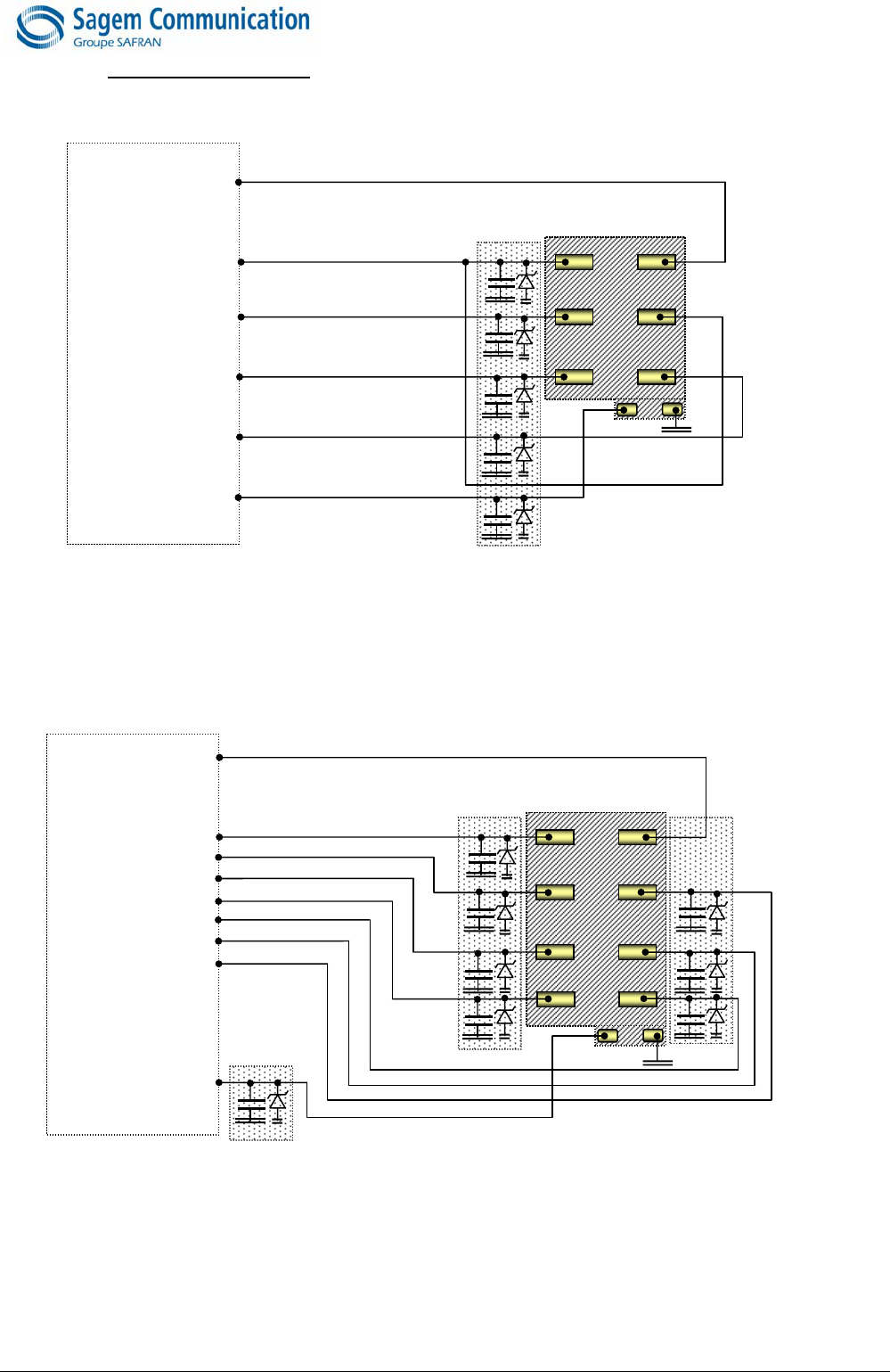
3.1.1.2 With SIM card detection
Normal SIM card case: 6 pins are used.
Figure 7
SIM card connection with presence detection
SIM Plus card case: 8 pins are used.
Figure 8
8 pins SIM plus card connection with presence detection
These configurations allows the module to detect if a SIM card is present in the connector or not. When present,
the SIMCD signal is connected to GND signal through a mechanical switch integrated in the SIM connector (the
type of switch depends of the SIM connector) thus a hardware interruption is generated. When the switch is
opened, the internal MO300 pull up raise the signal to high level (1.8V)
GND
SIMVCC
SIMRST
SIMCLK
SIMIO
SIMCD*
VCC
RST
CLK I/O
VPP
GND
SIM connector
MO300
CNT1 CNT2
GND
SIMVCC
SIMRST
SIMCLK
SIMPLUS
_
DATA
SIMPLUS_CMD
SIMIO
SIMPLUS_CLK
SIMCD*
VCC
RST
CLK I/O
SP_CLK
GND
SIM connector
SP_DATA SP_CMD
CNT2
page 12/46
Note d’étude / Technical document : URD1 – 5625.1 – 006 / 69796 Edition 03
Document Sagem Communication Reproduction et divulgation interdites
Sagem Communication document. Reproduction and disclosure prohibited
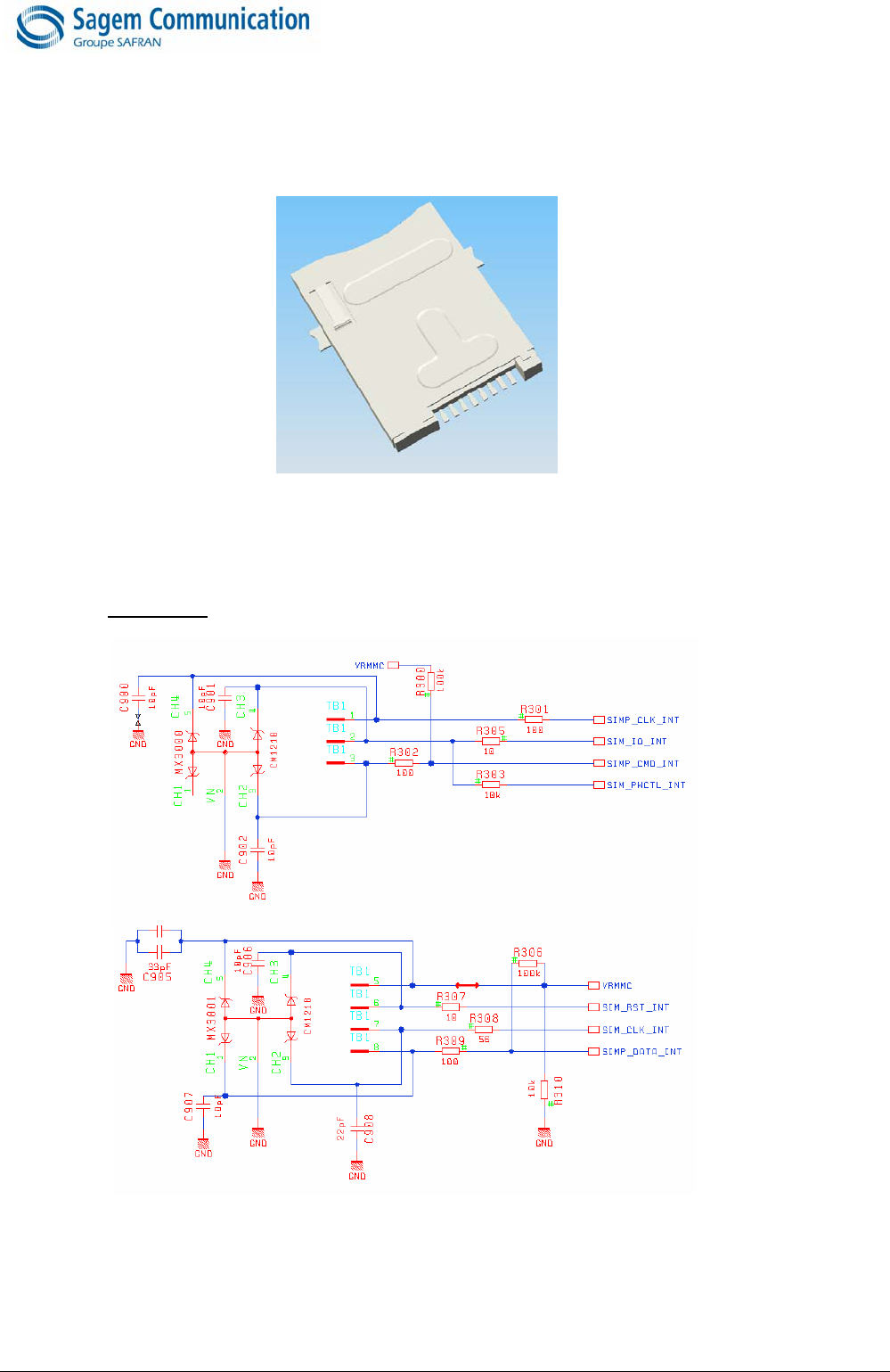
3.1.2 SIM holder soldered on the back of the MO300.
The MO300 module feature a soldering area on its back to mount a Sim card holder with all necessary
components to protect it from EMC and ESD.
For your design, if the Sim connection through the BtB connector is not required, use the following
recommended schematic.
As already warned: Never use both SIM card connection solutions at the same time. This is mandatory.
Figure 9 SIM holder
The behaviour is as described in the previous chapter.
3.1.2.1 Schematics
Figure 10
Components for backside Sim holder
Note: SIM card presence detector cannot be used with the SIM holder on the back of the MO300. The
SIMCD signal is therefore not used in that case.
page 13/46
Note d’étude / Technical document : URD1 – 5625.1 – 006 / 69796 Edition 03
Document Sagem Communication Reproduction et divulgation interdites
Sagem Communication document. Reproduction and disclosure prohibited
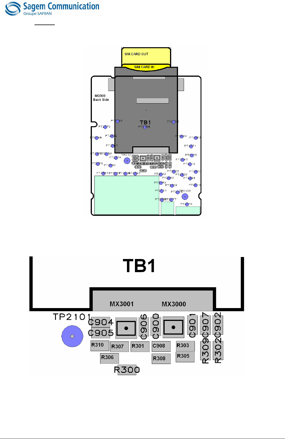
3.1.2.2 Placing
All these components should be soldered at the following positions.
Figure 11
Components for backside SIM holder
Close view of the components area:
Figure 12
Zoom on components area
SAGEM can provide a suppliers component codes list on request
page 14/46
Note d’étude / Technical document : URD1 – 5625.1 – 006 / 69796 Edition 03
Document Sagem Communication Reproduction et divulgation interdites
Sagem Communication document. Reproduction and disclosure prohibited
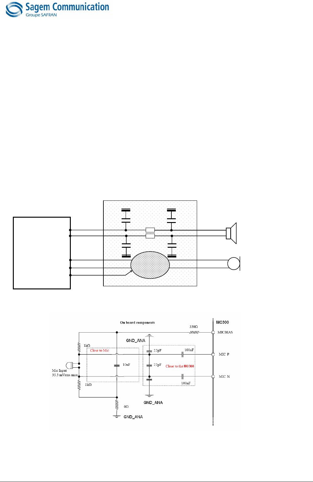
3.2 HOW to connect the AUDIOS?
The MO300 module feature 2 differential audio paths. A main audio path to connect a microphone and a
speaker, and a second one to connect an auxiliary audio through a Jack (for example). In this following chapter
examples of design will be given including protections against EMC and ESD and some notes about the routing
rules to follow to avoid the TDMA noise usually present in this sensitive area of design. It will also give the way
to use the hook function and the audio-jack presence detector.
3.2.1 Using a differential Handset mode on the main audio path
The MO300 can manage an external microphone (MICP/MICN) and external speaker (32 ohms SPKP/SPKN) in
differential mode.
Thus, one receiver and one microphone can be connected to the module with the following characteristics (see
SAGEM references):
- Receiver 32 ohms up to 120 ohms
- Microphone accepting the polarisation described below (FET Buffer + Open Drain).
- The microphone can be supplied using the internal MO300 bias supply (recommended but not mandatory)
or any other external bias system compliant with selected microphone within the MO300 inputs limits.
Figure 13
Differential audio handset mode
Figure 14
Microphone on board components
Protective components
speaker
MO300
SPKP
SPKN
MICP
MICN
2.0V / 2.5V
MICBIAS
+
47nH
15pF
22pF
15pF
22pF
47nH
Micro
p
hone
See
Application
schematic
page 15/46
Note d’étude / Technical document : URD1 – 5625.1 – 006 / 69796 Edition 03
Document Sagem Communication Reproduction et divulgation interdites
Sagem Communication document. Reproduction and disclosure prohibited
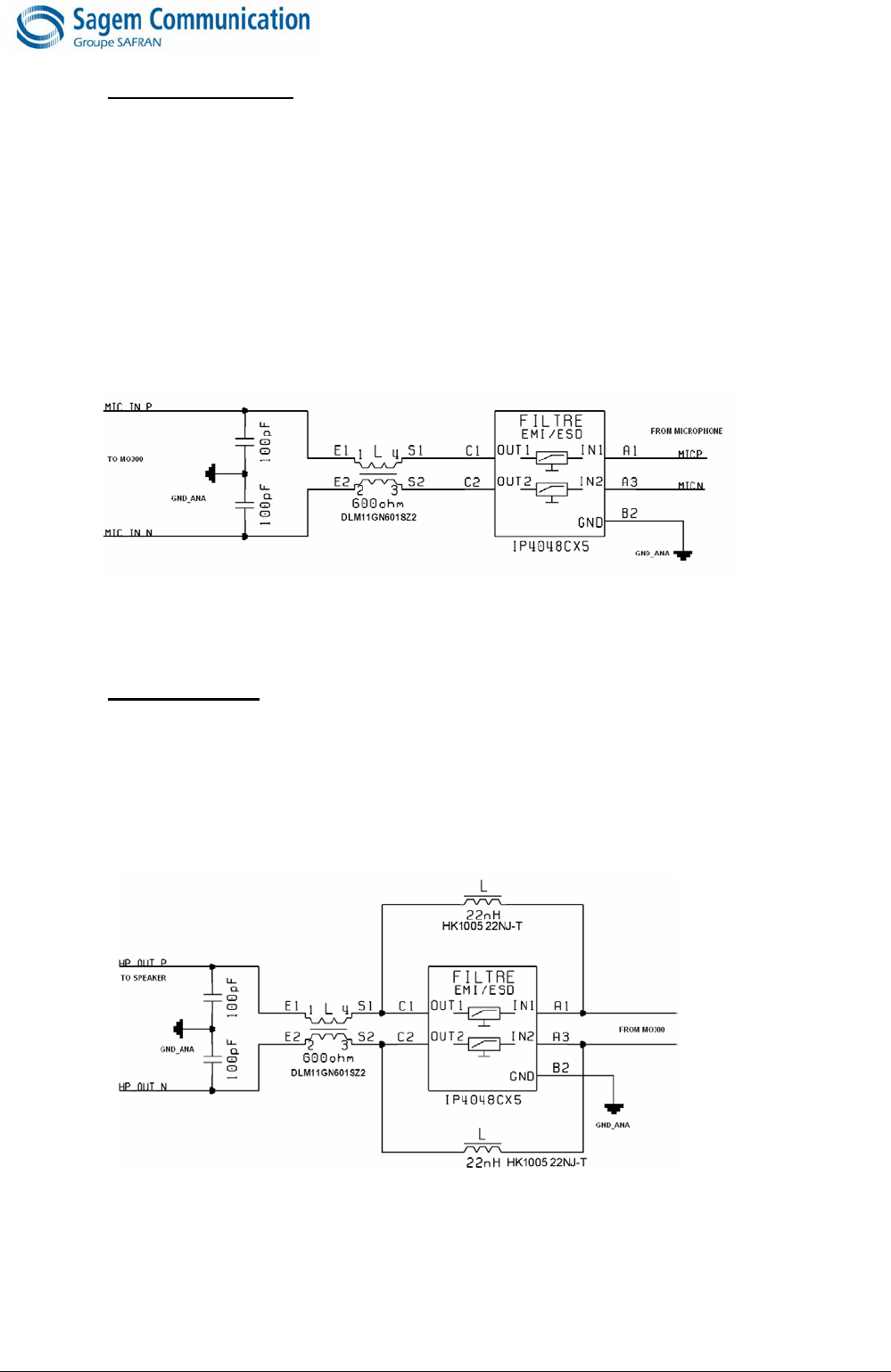
3.2.1.1 Notes for microphone
• Pay attention to the microphone device, It must not be sensitive to RF disturbances.
• Some microphone includes two spatial microphones inside the same shell and allow to make an
electrical difference between the environment noise (received by one of the two mic.) and the
active signal (received by the other mic. + noise) resulting in a very high SNR.
• Some resistors and capacitors should be connected as near as possible to the module as shown
in the figure.
• If you Need to have deported microphone out of the board with long wires, you should pay
attention to the EMC and ESD effect. It also the case when your design is ESD sensitive. In
those cases, add the following protections to improve your design.
• To ensure proper operation of such sensitive signals, they have to be isolated from the others by
analogue ground on mother board layout. (Refer to Layout design chapter)
Figure 15
EMC& ESD protections for microphone in case of need
3.2.1.2 Notes for speaker
• For the speaker external π filters have to be added as near as possible to the speaker to
suppress external disruption.
• Moreover, as explained for the microphone, if the speaker is deported out of the board or is
sensitive to ESD, use the schematic here after to improve the audio.
• SPKP ,SPKN, and tracks must be larger than other tracks: 0.3mm .
• As described in the layout chapter, differential signals have to be routed in parallel: it is the case
for SPKP, SPKN, MICP and MICN.
Figure 16
EMC& ESD protections for speaker in case of need
page 16/46
Note d’étude / Technical document : URD1 – 5625.1 – 006 / 69796 Edition 03
Document Sagem Communication Reproduction et divulgation interdites
Sagem Communication document. Reproduction and disclosure prohibited
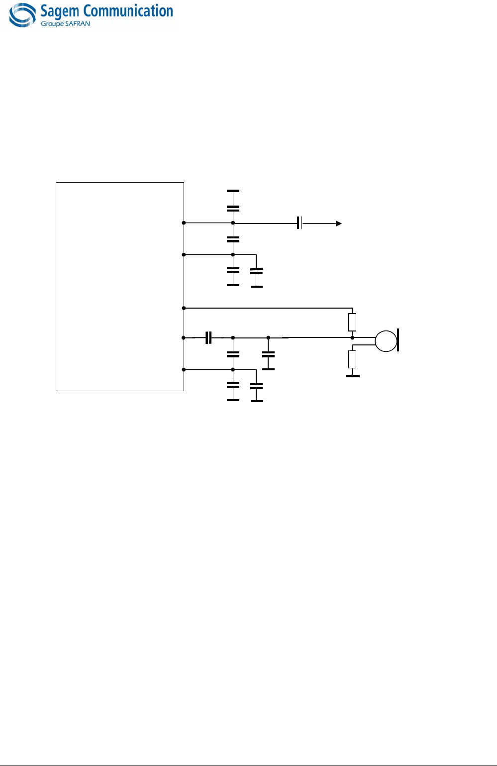
3.2.2 Non differential audio handset
For a better rejection of the common mode it is recommend to use differential audio lines.
In case, customer wants to implement a non differential solution, the figure below shows an example.
The microphone can be supplied using the internal MO300 bias supply (recommended but not mandatory) or
any other external bias system compliant with selected microphone within the MO300 inputs limits.
Note:
SPKN and MICN must not be grounded
SPKN must not be connected to SPKP
MICN must not be connected to MICP
Figure 17
Non differential audio connections
Note:
If this design is ESD or EMC sensitive do not hesitate to improve it using the advises given in those chapters :
• Notes for microphone
• Notes for speaker
The weakness can either come from your PCB routing and placement or from the chosen components (or
both).
• This design is an example of single audio connection for both microphone and speaker. Only a part of it
can be chosen depending on your project request (i.e. single microphone and differential speaker or vice-
versa).
Micro
22pF +
MO300
SPKP
SPKN
2.0V / 2.5V MICBIAS
MICP
MICN
22pF
22pF
22pF 1µF
22
p
F
22pF
1
µ
F
68
µ
F
Power amplifier
or Speaker
100nF
+
1KΩ
1KΩ
page 17/46
Note d’étude / Technical document : URD1 – 5625.1 – 006 / 69796 Edition 03
Document Sagem Communication Reproduction et divulgation interdites
Sagem Communication document. Reproduction and disclosure prohibited
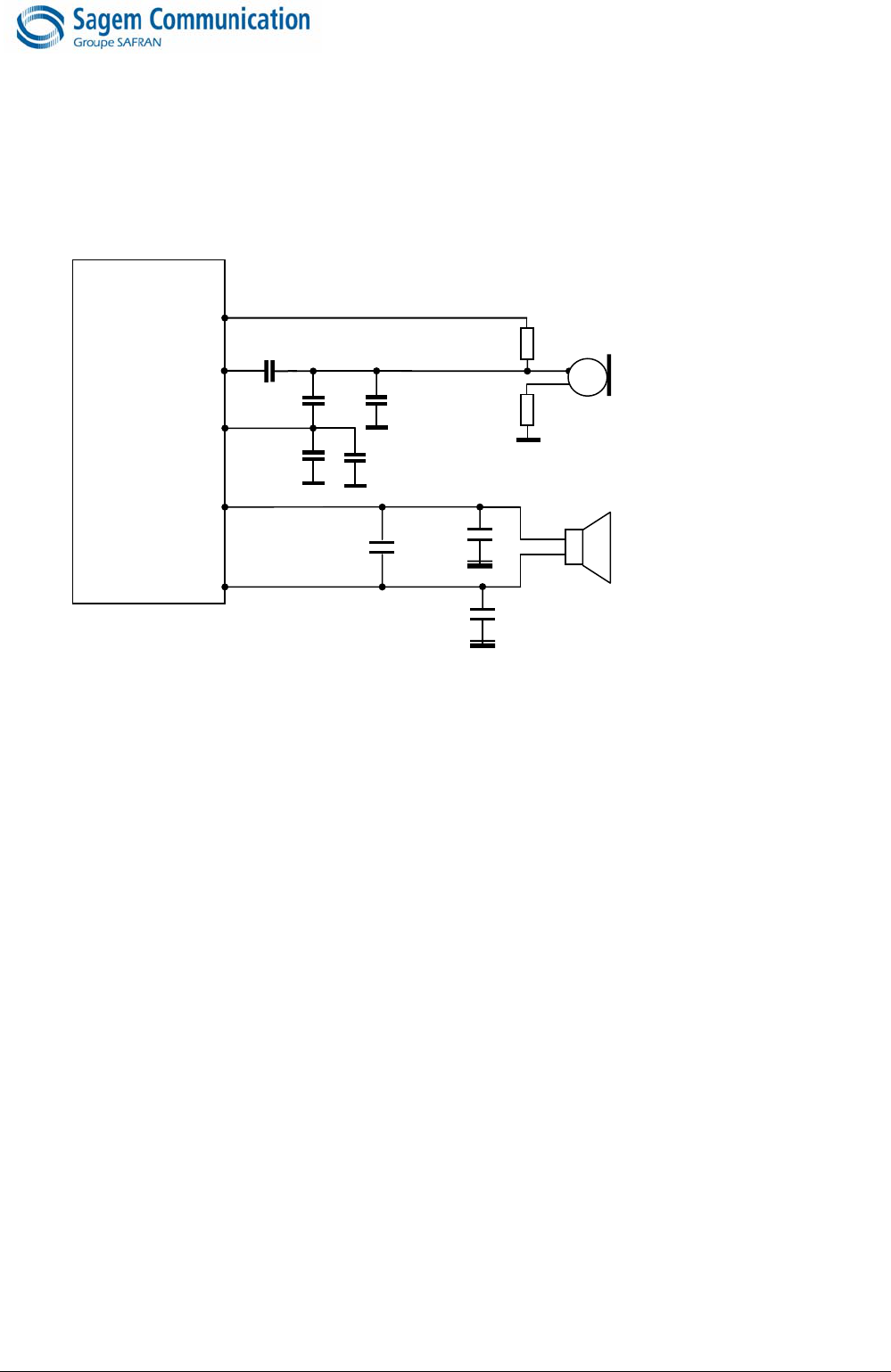
3.2.3 Using a mono Headset mode on the secondary audio path
MO300 features a secondary audio path dedicated to be used with a Hands free kit accessory.
This audio path can also be used instead of the main depending on the required audio power.
An external microphone and earphone (32 ohms) can be connected to the MO300
Since the input unlink path is differential only mono headsets are supported, the speaker is connected between
HSOR and HSOL.
The microphone can be supplied using the internal MO300 bias supply (recommended but not mandatory) or
any other external bias system compliant with selected microphone within the MO300 inputs limits.
Figure 18
Mono audio headset
Note: The capacitors have to be close to the external connector.
3.2.4 Audio interface selection
In order to switch from one selection to the other, AT commands shall be used to configure the audio paths in
case "SGV" file is used by default.
Refer to relevant paragraph of document [ 2 ] to implement AT commands.
3.2.5 Multi Channel Serial Interface
A MCSI bus is provided on the module MO300 for a digital interface application ( i.e. Bluetooth).
Characteristics are the following :
- Voice samples : 16bits, 8kHz
- MCSI Clock : 520 kHz
- Voltage : 1.8V
More details can be given on request.
2.0V / 2.5V
MICBIAS
HSMICIP
HSMICIN
HSOR
HSOL
22pF
MO300
22pF
22pF
22pF
22pF
22pF 1µF
100nF
+
1KΩ
1KΩ

page 18/46
Note d’étude / Technical document : URD1 – 5625.1 – 006 / 69796 Edition 03
Document Sagem Communication Reproduction et divulgation interdites
Sagem Communication document. Reproduction and disclosure prohibited
3.2.6 Characteristics of the microphone and speaker recommended by SAGEM
3.2.6.1 Characteristics of the microphone recommended by SAGEM
Item to be inspected Acceptance criterion
Sensitivity -32 dB SPL +/- 3 dB (0 dB = 1 V/Pa @ 1kHz) or
-40 dB SPL +/- 3 dB (0 dB = 1 V/Pa @ 1kHz)
Frequency response Limits (relatives values)
Freq. (Hz) Lower limit Upper limit
100 -1 +1
200 -1 +1
300 -1 +1
1000 0 0
2000 -1 +1
3000 -1.5 +1.5
3400 -2 +2
4000 -2 +2
Current consumption 1 mA (maximum)
Operating voltage DC 1 to 3 V (minimum)
S / N ratio 55 dB minimum (A-Curve at 1 kHz, 1 Pa)
Directivity Omni-directional
Maximum input sound pressure level 100 dB SPL (1 kHz)
Maximum distortion 1%
Radio frequency protection Over 800 - 1200 MHz and 1700 - 2000 MHz, S/N ratio 50
dB minimum (signal 1 kHz, 1 Pa)
3.2.6.2 Characteristics of the dual mode speaker recommended by SAGEM
Inspection non operating
Item to be inspected Acceptance criterion
Input power: rated / max 0.5 W / 1 W
DC Impedance 6 Ω +/- 10 %
Resonance frequency (Fo) 480 Hz +/- 10%
Magnetic field < 50 Gauss at 5 mm on the back side of the speaker
Weight < 3.0 g
Inspection operating
Test condition: Receiver is measured with IEC 318 coupler in sealed condition
Item to be inspected Acceptance criterion
Frequency response
Input Voltage: 60mVrms
Freq Lower limit Nom. value Upper Limit
(Hz) (dBSPL) (dBSPL) (dBSPL)
200 119 121 123
400 122 124 126
700 125 127 129
800 125 127 129
1000 120 122 124
1500 111 113 115
2000 108 110 112
3000 103 105 107
4000 98 100 102
S / N ratio 50 dB minimum (A-Curve at 1 kHz, 1 Pa)
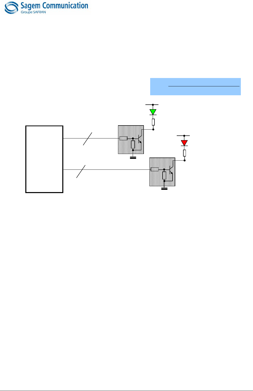
3.3 Network LEDs
The MO300 module can manage two PWM outputs, for example to drive two network LED.
These LED could be used to interact with the network activity and the MO300 states.
page 19/46
Note d’étude / Technical document : URD1 – 5625.1 – 006 / 69796 Edition 03
Document Sagem Communication Reproduction et divulgation interdites
Sagem Communication document. Reproduction and disclosure prohibited
If more than two LED are required, any GPIO can be used to drive a LED. A maximum of 10 GPIO are available
on the MO300 Module.
3.3.1 Network LEDs connection.
Green LED shall be connected to LED1, Red LED shall be connected to LED2, serial resistor shall be
connected to each LED.
These transistors can be found a in a single package referenced as UMDXX or PUMDXX Family.
Value of resistor depends on characteristic of chosen LED, it is used to limit the current through the diode,
Consider this formula to compute the resistor value in worst case:
min
maxminmin
max Id
)Vcesat (Vd - Vbat
R +
=
Figure 19
Network LED connection
3.3.2 Network LEDs behaviour.
As LEDs are driven through PWM outputs of the MO300, they can be configured with appropriate AT
command.
User application can set for each output :
- Period between : 125ms and 3000ms
- Time on between : 3,889 and 93,59 ms
More details can be found in AT document referenced [ 2 ].
LED1
MO300
LED2
1 VBAT
1
VBAT
R
R
page 20/46
Note d’étude / Technical document : URD1 – 5625.1 – 006 / 69796 Edition 03
Document Sagem Communication Reproduction et divulgation interdites
Sagem Communication document. Reproduction and disclosure prohibited
3.4 Power supply
The MO300 module can be supplied by battery or any DC/DC converter compliant with the module supply
range 3.3Vmin and up to 5.5Vmax 2A.
The PCB tracks must be well dimensioned to support 2A maximum current.
Maximum serial resistance on VBAT = 170mΩ internal resistance of the battery plus tracks and contact
resistance of the connectors for a new battery, or tracks & contact resistance of the connectors for a DC/DC
converter.
Case of old batteries: If this value is overran, this can cause erratic reset of the module when the
battery begins to be discharged.
The VBAT_CNT signal disturbs the other signal; it has to be isolated with ground from the other signals,
especially radio and audio signals.
In case of batteries, it is mandatory to use Li-Ion or Li-Polymer batteries.
NOTE: The MO300 M2M module does not manage the charge of any kind of batteries.
3.5 V24 UART
The MO300 module feature a V24 UART interface plus a USB2 OTG interface to communicate with the Host
through AT commands or for easy firmware upgrading purpose.
3.5.1 Complete V24 – connection MO300 - host
A V24 UART interface is provided on the main connector of the MO300 module with the following signals:
RTS/CTS, RXD/TXD, DSR, DTR, DCD, RI.
It is recommended to manage an external access to the V24 interface, in order to allow easy software upgrade,
especially when USB is not planed to be used.
Figure 20
Complete V24 UART connection between MO300 and host
3.5.2 Complete V24 interface with PC
It supports speeds up to 115.2 KBPS and may be used in auto bauding mode as well.
To use the V24 interface, some adaptation components are necessary to convert the +1.8V signals from
the MO300 to +5V signals compatible with a PC.
RXD
TXD
RTS
CTS
MO300
DCD
DTR
DSR
RI
GND
RXD
TXD
RTS
CTS
Host
DCD
DTR
DSR
RI
GND
page 21/46
Note d’étude / Technical document : URD1 – 5625.1 – 006 / 69796 Edition 03
Document Sagem Communication Reproduction et divulgation interdites
Sagem Communication document. Reproduction and disclosure prohibited
An example of connection between MO300 and a PC is given below.
Figure 21
Signal adaptation using Level Shifters and RS232 Transceiver.
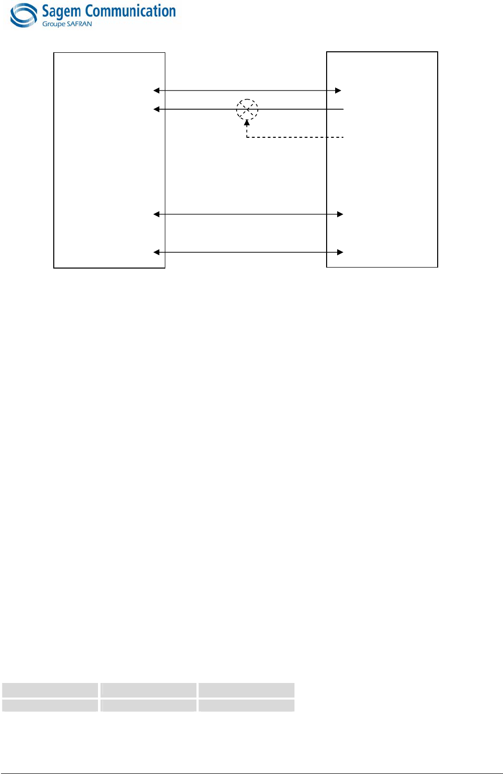
3.5.3 Partial V24 ( RX-TX-RTS-CTS) – connection MO300 - host
When using only RX/TX/RTS/CTS instead of the complete V24 link, we recommend following schematic:
As we need DTR active (low electrical level), a loop DSR on DTR is sufficient because DSR is active (low
electrical level) once the XS200 is switched on.
DCD and RI can stay not connected and floating.
Figure 22
Partial V24 connection (4 wires) between MO300 and host
RXD
TXD
RTS
CTS
MO300
DCD
DTR
DSR
RI
GND
RXD
TXD
RTS
CTS
Host
DCD
DTR
DSR
RI
GND
page 22/46
Note d’étude / Technical document : URD1 – 5625.1 – 006 / 69796 Edition 03
Document Sagem Communication Reproduction et divulgation interdites
Sagem Communication document. Reproduction and disclosure prohibited
3.5.4 Partial V24 ( RX-TX) – connection MO300 - host
When using only RX/TX instead of the complete V24 link, we recommend following schematic :
We need DTR active (low electrical level), a loop DSR on DTR is sufficient because DSR is active (low
electrical level) once the MO300 is switched on.
We also need RTS active (low electrical level), a loop RTS on CTS is sufficient because CTS is active (low
electrical level) once the MO300 is switched on.
DCD and RI can stay not connected and floating.
Figure 23
Partial V24 connection (2 wires) between MO300 and host
3.6 UART 2
It is strongly recommended to let this interface externally accessible for Debug (e.g. access by 2 tests pads).
TXD2 and RXD2 can be used to get the software traces.
3.7 USB 2.0 OTG
The USB 2.0 interface is Full speed, then has a maximum rate of 12Mbit/s. It is On The Go capable then can be
in slave or Master mode depending on the connected equipment and the MO300 Version.
MO300 can only be in slave mode. Master mode and capability to switch between the two modes is only
available with the MO300E module.
In slave mode, the MO300 is answering to the customer application which is the Master of the communication.
RXD
TXD
RTS
CTS
MO300
DCD
DTR
DSR
RI
GND
TXD
RXD
RTS
CTS
Host
DCD
DTR
DSR
RI
GND
page 23/46
Note d’étude / Technical document : URD1 – 5625.1 – 006 / 69796 Edition 03
Document Sagem Communication Reproduction et divulgation interdites
Sagem Communication document. Reproduction and disclosure prohibited
Figure 24
USB Connection between MO300 and host
To use USB link between Host and MO300, specific SAGEM USB drivers are needed and available on SAGEM
www site and on request.
As soon as USB link is detected by the MO300 module, the AT command responses are sent on USB link and
RS232 - UART1 interface is de-activated.
RS232 - UART2 interface for traces is still operational.
USB and RS232 - UART1 are then exclusive and priority is given to the USB interface.
CMD I/O command can be used if required, see "Stopping the module" chapter.
3.8 Backup battery
3.8.1 Backup battery function feature
A backup battery can be connected to the module in the aim to supply internal RTC (Real Time Clock) when the
main battery is removed. Thus, when the main battery is removed, the RTC is still supplied. Otherwise, user will
have to set the date and time after the next start.
With external BACKUP:
- if VBAT < VBACKUP, internal RTC is supplied by VBACKUP.
- if VBAT > VBACKUP, internal RTC is supplied by VBAT.
If there is no backup battery, VBACKUP input of the module has to be connected to VBAT signal.
Without external VBACKUP (VBACKUP input connected to VBAT)
- if VBAT > 2.2V, internal RTC is supplied by VBAT.
- if VBAT < 2.2V, internal RTC is not supplied.
Signal Min Max
VBACKUP +1.8V +3.2V
USB ID
VBUS
MO300 (device)
D +
D -
USB ID
VBUS
CMD
Host
D +
D -
page 24/46
Note d’étude / Technical document : URD1 – 5625.1 – 006 / 69796 Edition 03
Document Sagem Communication Reproduction et divulgation interdites
Sagem Communication document. Reproduction and disclosure prohibited
3.8.2 Current consumption on the backup battery
When the Main battery is removed, the current consumption which is supplied by the backup battery changes,
depending on its voltage level.
The following table sum up the three different states:
VBACKUP (V) Typical value of current Consumption (µA)
2.4 < VBACKUP 50
2.15 < VBACKUP < 2.4 Linear decrease from 250 (at 2.15V) to 50 (at
2.4V)
1 <VBACKUP < 2.15 Linear growth from 50 (at 1 V ) to 250 (at 2.15V)
These values have to be taken into account for the choice of the Backup Battery technology and model.
3.8.2.1 Charge by internal MO300 charging function
The charging function is available on the MO300 without any additional external Power supply (the charging
power supply is provided by the MO300).
The recommended schematic is given hereafter:
Figure 25
Backup battery internally charged
The resistor R depends on the charging current value provided by the battery manufacturer, R=100 Ohm has
been tested with a capacitor battery.
The characteristics of the charging function done by the MO300 is given hereafter:
Conditions of test Min (µA) Typ(µA) Max(µA)
V backup = 12 mV (deep
discharge)
350 550 900
V backup = 2.8 V 350 550 900
If the recommended schematic is implemented by the customer, SAGEM will set a dedicated parameter in the
software which will automatically manage the charging function.
The advantages of this management are:
• saving of component on the MAIN board,
• saving of available surface on the MAIN board,
• regulated charging current (independent of VBAT value) for the backup battery,
• improve overall power management.
MO300
R
+
VBACKUP

page 25/46
Note d’étude / Technical document : URD1 – 5625.1 – 006 / 69796 Edition 03
Document Sagem Communication Reproduction et divulgation interdites
Sagem Communication document. Reproduction and disclosure prohibited
3.8.3 Backup Battery technology recommended
3.8.3.1 Manganese Silicon Lithium-Ion rechargeable Battery
Sagem does not recommend to use this kind of technology because of the following drawbacks:
• the maximum discharge current is limited (Shall be compliant with the module characteristics)
• the over-discharge problem: most of the Lithium Ion rechargeable batteries are not able to recover their
charge when their voltage reaches a low-level voltage. To avoid this, it is necessary to add a safety
component to disconnect the backup battery in case of over–discharge condition. In such a case, this
implementation is too complicated (too much components for that function).
• The charging current has to be regulated
SAGEM does not recommend to use this kind of backup battery technology at all.
3.8.3.2 Capacitor Battery
These kinds of backup battery have not the drawbacks of the Lithium Ion rechargeable battery.
As there are only capacitors:
• the maximum discharge current is generally bigger,
• there is no problem of over-discharge: the capacitor is able to recover its full charge even if its voltage has
previously fallen to 0V.
• there is no need to regulate the charging current.
Moreover, this kind of battery is available in the same kind of package than the Lithium Ion cell and fully
compatible on a mechanical point of view. The only disadvantage is that the capacity of this kind of battery is
significantly smaller than Manganese Silicon Lithium Ion battery. But for this kind of use (supply internal RTC
when the main battery is removed), the capacity is generally enough.
SAGEM strongly recommends to use this kind of backup battery technology.
3.9 General Purpose Input Output
Ten General Purpose Input Output (GPIO) are available on the board to board connector. The customer
application can directly use them through the appropriate AT command as :
- output : pin is set to High or Low state
- input : pin is read on request and answer is given to the customer application.
As input, different cases are possible to cover the maximum possible of customer application :
- synchronous answer to the AT command (*)
- Asynchronous answer to the AT command. The customer application previously to the request has
configured the GPIO to react on falling/rising edges. The customer application is notified asynchronously by
AT command answer when the configured trigger occurs.
(*) : AT command process is not dedicated to real-time process. Then, driving the GPIO through this AT
command is not aimed to emulated fast transient signals.
All details to drive GPIO are given in AT commands document [ 2 ].
3.10 Temperature sensor
One temperature sensor is available on the MO300 module. Its is located on the MO300 PCB (near the board
to board connector) and not under the MO300 shield in order to give the ambient temperature of the customer
application.
Due to the fast react and sensitivity of the temperature sensor, the result can be more or less accurate
depending on possible draughts affecting the sensor. To give more precise results, the temperature sensor
must be , as far as possible, isolated from draughts in the customer design.
The temperature sensor covers all the operational temperature range of the MO300 module.
The temperature can be read on request through appropriate AT commands as described in AT commands
document [ 2 ].
page 26/46
Note d’étude / Technical document : URD1 – 5625.1 – 006 / 69796 Edition 03
Document Sagem Communication Reproduction et divulgation interdites
Sagem Communication document. Reproduction and disclosure prohibited
3.11 ADC
The ADC value can be read by the specific AT command as defined in the document referenced [2]. The input
limits are the following: from 0V up to 1750mV
The returned value is on 10 bits converted to decimal.
3.12 Micro-wire Bus
The microwire bus is available but the client has to ask SAGEM to develop the driver and the specific
application related the connected device.
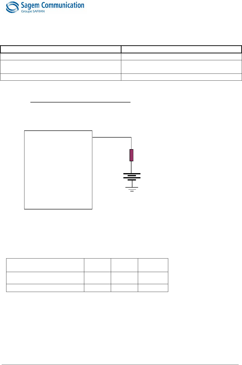
3.13 Antenna detection
Antenna detection can be provided if following criteria are met :
• Antenna design is performed according to design given below.
• Feature is activated through AT command.
AT command answer can be synchronous or asynchronous depending on customer request, as described in
AT command document referenced [ 2 ].
L
MO300
Antenna contacts
A coil L of 39µH must be added inside the
antenna connector.
Antenna
Antenna connector
50Ω track
page 27/46
Note d’étude / Technical document : URD1 – 5625.1 – 006 / 69796 Edition 03
Document Sagem Communication Reproduction et divulgation interdites
Sagem Communication document. Reproduction and disclosure prohibited
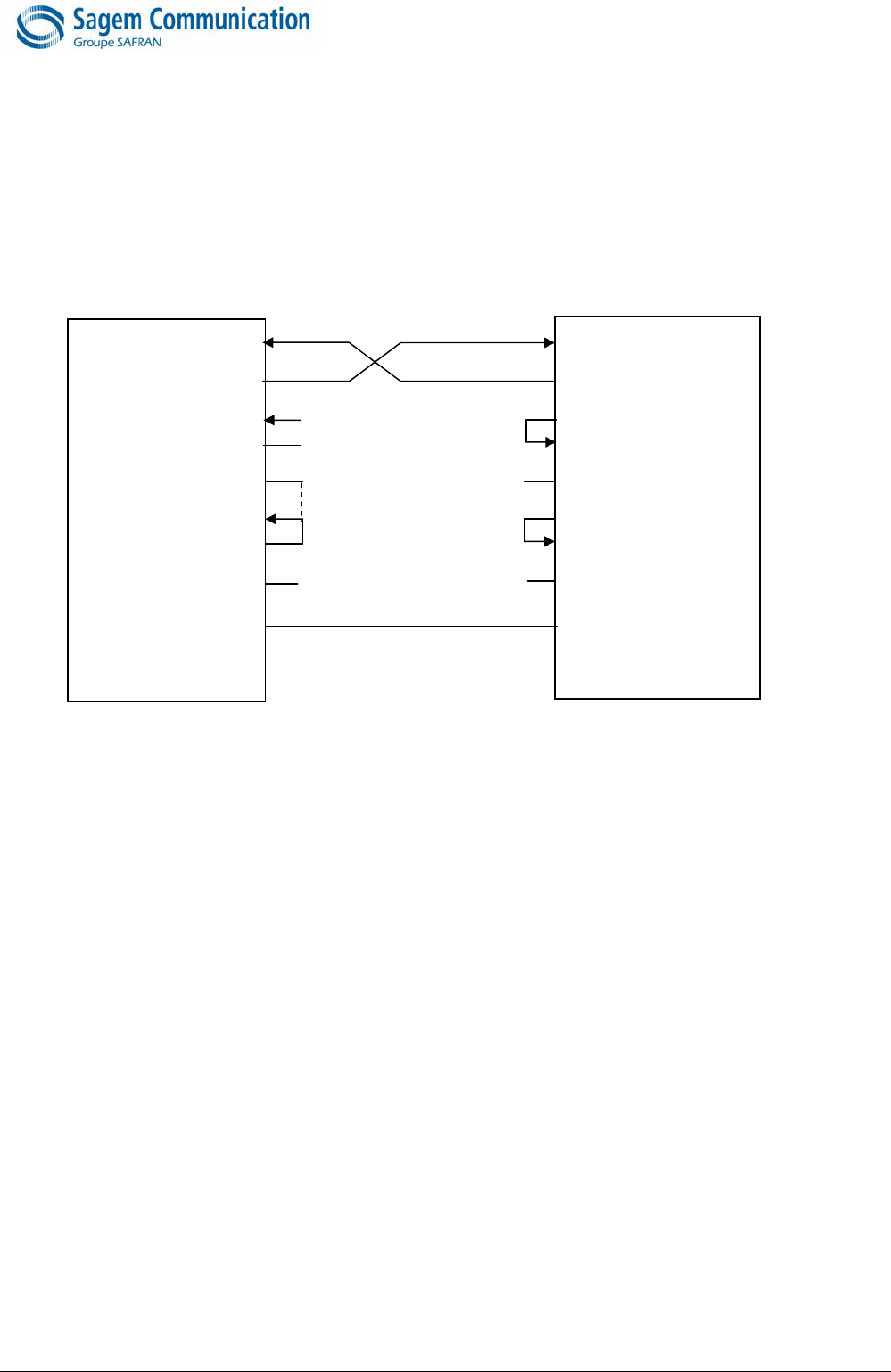
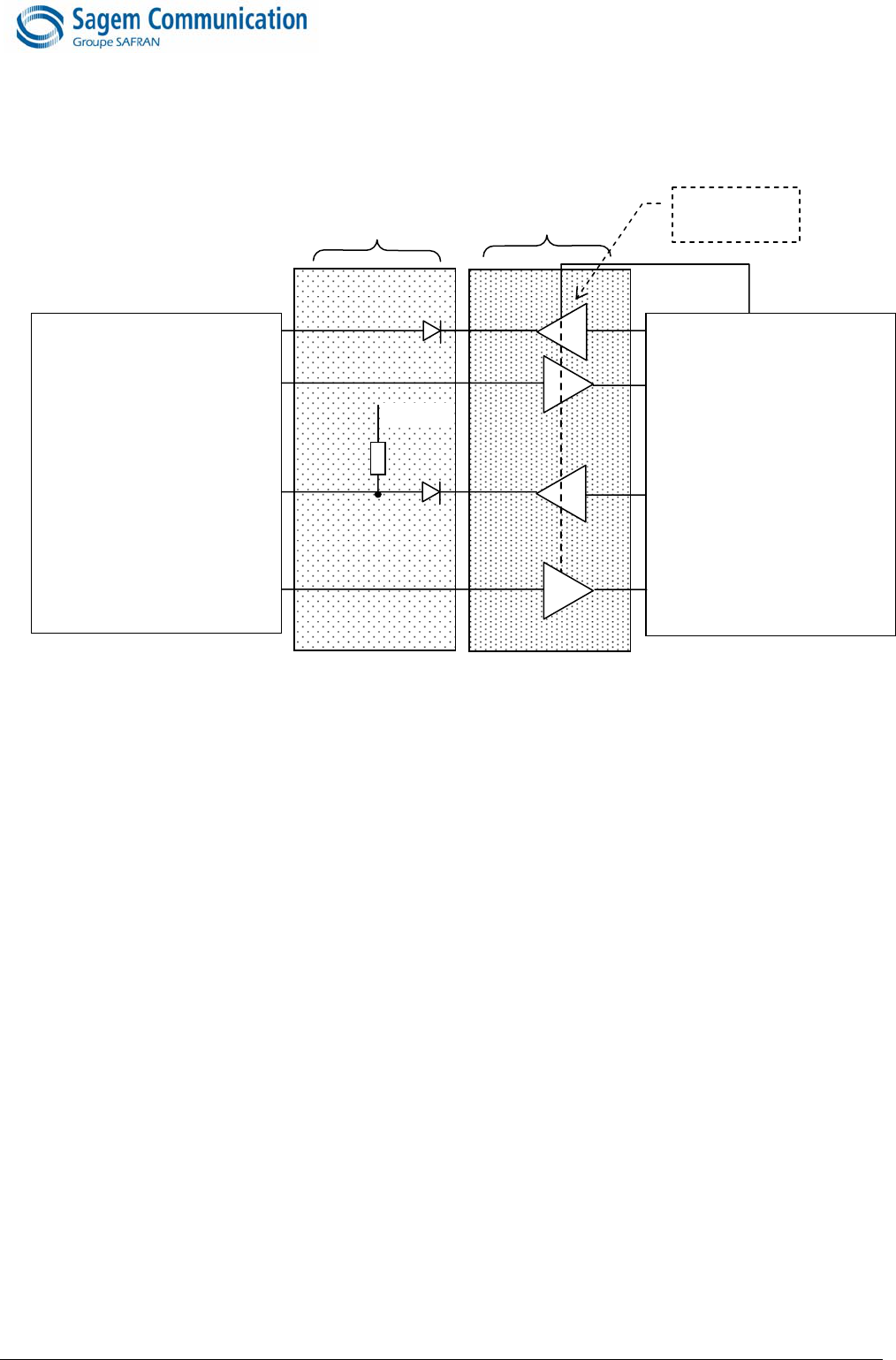
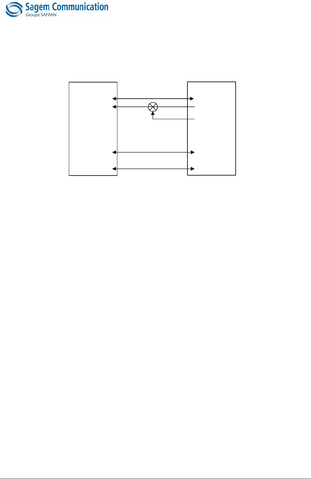
3.14 Hardware Power management and multiplexing interfaces
In case hardware power management and multiplexing are used, it is necessary to isolate host and module
MO300 in order to not generate current re-injection when MO300 is switched-off.
Typical schematics (only useful signals are represented):
Figure 26
Hardware interface between MO300 and host
In a general case, solution 1 ( cheaper) is enough to protect the module MO300.
3.15 Resetting the module
The MO300 module supports 2 kinds of reset:
• External software reset activated by the AT command as defined in the document referenced [2]
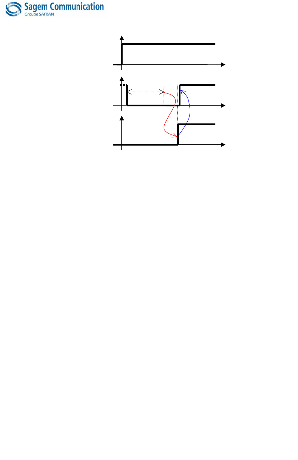
• External level 1 priority Hardware reset by pulling down the PWON* signal more than 8.2 seconds, on the
next rise of PWON* the module is trigged. The reset is done 8.2 seconds later. This hardware reset, resets
all the registers as well as the real time clock register, it is unconditional and have the highest priority. The
module is in off mode after this hardware reset and need a new starting sequence to start again. At least
16.4 seconds are necessary to perform the hardware reset.
3.16 Starting the module
There are two ways to start the MO300 module.
3.16.1 Use of PWON*
First power up VBAT, which must be in the range 3.3V – 4.5V, and able to provide at least 2A during the TX
bursts (refer to the module specification for more details).
To start the module, a low level pulse must be sent on PWON* during more than 31.25ms (at 25°C). This
duration increases as the temperature decreases (up to ~ 1 second at –30°C).
After ~3 seconds CTS is active and so MOD_ON_STATE when it is ready to receive AT commands.
To be sure that the pulse duration is enough to start the module, independently from the temperature,
MOD_ON_STATE can be used as feedback to stop the pulse:
DTR,RTS, RXD
CTS, DSR, DCD, RI, TXD
DTE_UART*_STATE,
MOD_RESET_STATE,
MOD_UART_STATE,
MOD_FLOW_STATE,
MOD_ON_STATE
Tri-state command
MO300
HOST
(
PC
)
VREXTH
Tri-state
Buffers
100K
Solution 1 Solution 2
page 28/46
Note d’étude / Technical document : URD1 – 5625.1 – 006 / 69796 Edition 03
Document Sagem Communication Reproduction et divulgation interdites
Sagem Communication document. Reproduction and disclosure prohibited
VBAT
PWON*
t
MOD_ON_STATE
31.25ms
Figure 27
Suggested starting sequence
3.16.2 Case of USB Plugged
First power up VBAT, which must be in the range 3.3V – 4.5V, and able to provide at least 2A during the TX
bursts (refer to the module specification for more details).
To start the module, plug an USB data cable to the PC then plug it to the module. The module detects the
VBUS signal and start automatically.
MOD_ON_STATE can be used as feedback to know the module state.
3.17 Stopping the module
3.17.1 Case of UART Interface
To stop the module, use the AT command AT+CPOF, as defined in the document AT commands for MO300
series modules. If the Pwon* is not pulled down the module will turn in OFF mode after the AT command,
otherwise the module restarts immediately (an OFF sequence is performed followed by a power ON sequence).
Note: The MO300 module stops automatically after few minutes when :
• the sim card requests a pin code which is not entered
• no sim card is present.
page 29/46
Note d’étude / Technical document : URD1 – 5625.1 – 006 / 69796 Edition 03
Document Sagem Communication Reproduction et divulgation interdites
Sagem Communication document. Reproduction and disclosure prohibited
3.17.2 Case of USB Interface
As the module can also start when an USB cable is plugged, the sequence to stop the module needs the USB
interface to be OFF or VBUS disconnected just after the command is sent and acknowledged by the module.
Thus, to stop the module when the USB interface is used, use the AT command AT+CPOF, as defined in the
document AT commands for MO300 series modules, then disconnect VBUS (unplug the USB cable or use a
commanded switch to switch of VBUS) signal when the module acknowledges (responds OK) the command,
otherwise the module restarts immediately (an OFF sequence is be performed followed by a power ON
sequence).
Figure 28
USB power command example
3.18 Sleep mode management
The module can save power consumption when it's in sleep mode. The module switchs off the unused I/Os and
LDOs to reduce the power consumption. When the module is in sleep mode the power consumption is reduced
to it's minimum, the module stays in sleep mode and only wakes up to listen to the paging blocks (still able to
receive calls).
The module MO300 features 3 sleeps mode: The management is done using the AT command, as defined in
the document AT referenced [2].
3.18.1 First mode
This mode allows the module to enter in sleep mode only when the DTE allows it. As long as the DTR signal is
low, the module does not go into sleep mode.
3.18.2 Second mode
This mode allows the module to decide to go into sleep mode by itself.
3.18.3 Third mode
This mode allows the module to go into sleep mode according to the hardware power management
specification using the 5 signals ( DTE_UART*_STATE, MOD_RESET_STATE, MOD_UART_STATE,
MOD_FLOW_STATE, MOD_ON_STATE ).
3.18.4 USB connectivity impact on sleep mode
When the USB interface is used, the MO300 module can not reach it's best power saving performances. The
MO300 module can not go into sleep mode as long as USB interface is active.
It is up to the Host responsibility to deactivate the USB connexion in order to allow sleep mode of the MO300
and then re-establish properly the USB connexion to communicate again with the MO300 module.
USB ID
VBUS
MO300
(DEVICE)
USB DP
USB DM
USB ID
VBUS
Command
HOST
USB DP
USB DM

page 30/46
Note d’étude / Technical document : URD1 – 5625.1 – 006 / 69796 Edition 03
Document Sagem Communication Reproduction et divulgation interdites
Sagem Communication document. Reproduction and disclosure prohibited
4 Mandatory points for the final tests and tuning
The design of the main board (which the module is connected to) must provide an access to following signals
when the final product will be completely integrated.
The module's firmware can be upgrade over serial or USB links. To proceed, SAGEM recommends that
products based on SAGEM modules provide a direct access to the module serial link or USB through an
external connector or any mechanism allowing the upgrade of the module without opening the whole product.
Minimum necessary serial link I/Os
TXD Output UART transmit 1
RXD Input UART receive 1
For the USB: the 4 USB points are necessary.

page 31/46
Note d’étude / Technical document : URD1 – 5625.1 – 006 / 69796 Edition 03
Document Sagem Communication Reproduction et divulgation interdites
Sagem Communication document. Reproduction and disclosure prohibited
5 ESD & EMC recommendations
5.1 Standard requirements for ESD
Test levels :
Contact discharge Air discharge
Test voltage (kV) Level Test voltage (kV) Level
2 1 2 1
4 2 4 2
6 3 8 3
8 4 15 4
Special X
1) Special X
1)
1) “X” is a level which has to be determined. This level is specified in the particular specification of the device. If
higher voltages as specified are needed, special testers have to be used.
Standard indicates that tests have to be done when module is in call connected to the main supply
(220V) trough any DC/DC converter. These tests consist to put some ESD impulses of 8 kV maximum
everywhere on the device. It mustn’t lose the call neither other functions and if one of them is lost, the
device has to come back in its normal configuration without external action.
Classification of test results :
N°1 : normal behaviour in specification limits
N°2 : temporary degradation or function loss or auto-recoverable behaviour
N°3 : temporary degradation or function loss or behaviour lost needing help of operator or a system reset
N°4 : irreparable degradation or function loss due to failure of material (components), software or data loss
5.1.1 ESD Analysis
ESD current can penetrate inside the device via the typical following components:
• SIM connector
• Antenna
• USB Connector
• UART Connector
• Audio Connectors
• DC power connector
• Battery
• All pieces with conductive paint
(Housing, etc...)
Therefore, in order to avoid ESD issues, efforts shall be done to decrease the level of ESD current on electronic
components located inside the device (main board, input of the module MO300, etc…)
5.1.2 Recommendations to avoid ESD issues
They can be summarised as below:
• Insure good ground connections of the module MO300 to the MAIN board
• Flex (if any) shall be shielded and FPC connectors shall be correctly grounded at each extremities
• Put capacitor 100nF on battery (not on charger), or better put Varistors or ESD diode in parallel
• Uncouple microphone and speaker by capacitor or Varistors in parallel of each wire of these devices

page 32/46
Note d’étude / Technical document : URD1 – 5625.1 – 006 / 69796 Edition 03
Document Sagem Communication Reproduction et divulgation interdites
Sagem Communication document. Reproduction and disclosure prohibited
5.2 ESD features
Using human body model from JEDEC JESD 22-A114 standard, the MO300 can hold 2kV on all MO300 pins
and contact areas such as antenna pads and connector. Except for the following pins where 1kV is supported
• SIM RST
• SIM CLK
• SIM IO
• SIMPLUS DATA
• SIMPLUS CLK
• SIMPLUS CMD
External protection with ESD diode can be added to have a stronger ESD protection.
5.3 EMC recommendations
In case of EMC issue due to a headset audio device, the solution may consist in inserting a filter on the wires
of the microphone and of the speaker.

page 33/46
Note d’étude / Technical document : URD1 – 5625.1 – 006 / 69796 Edition 03
Document Sagem Communication Reproduction et divulgation interdites
Sagem Communication document. Reproduction and disclosure prohibited
6 Recommended components
On request, SAGEM can provide the reference part numbers for the following recommended components:
Component SAGEM part
Handset microphone MIC1
Handset speaker HP1
Network Led LED1
SIM connector (with detection) SIM1
SIM connector (without detection) SIM2

page 34/46
Note d’étude / Technical document : URD1 – 5625.1 – 006 / 69796 Edition 03
Document Sagem Communication Reproduction et divulgation interdites
Sagem Communication document. Reproduction and disclosure prohibited
7 Radio integration
The module antenna connection has a characteristic impedance of 50 Ohms.
In order to get the best sensitivity and output power, it is recommended to implement a matching circuit between
the module and the antenna:
In order to design the matching circuit :
- test with direct connection in the first step
- adjust inductors and capacitors in a second step if needed
Test
point Module
MO300
50 ohm
Antenna
First step: 0 Ohm
First step: N.C.
First step: N.C.
page 35/46
Note d’étude / Technical document : URD1 – 5625.1 – 006 / 69796 Edition 03
Document Sagem Communication Reproduction et divulgation interdites
Sagem Communication document. Reproduction and disclosure prohibited
7.1 Antenna connection
MO300 module feature two ways to connect it to the GSM antenna.
7.1.1 Mini Coaxial connector
A mini-coaxial connector is provided on the MO300 : Hirose U.FL-R-SMT-1 (10)
7.1.2 Spring contacts
• 50 Ω line matching (between module and MAIN board, and with RF test point)
• SAGEM strongly recommends to solder the spring contact on the whole surface instead of only 2
points
Keep matching circuit on MAIN board but with direct connection in the first step – it could be necessary to make
some adjustment later, during RF qualification stage
Figure 29
Spring contact mounting
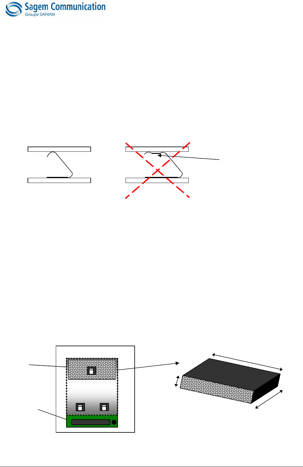
7.2 Ground link area
The MO300 feature 3 ground Pads for the RF. The 3 pads must be in contact with the ground plan of the main
board. Otherwise the RF performances will be degraded.
In case of need, if the 3 pads are not sufficient because of the client design, a metallic foam can be used as
described here after.
To have the best radio performances (spurious, sensitivity…),good ground contact between the module
shielding and the main board is needed using for example 0.5 / 0.7mm metallic foam or label. Do not solder the
shielding of the module on ground pad of the main board.
Conductive foam:
minimum size = 1cm x 3 cm (located on the top of MO300 shielding – near antenna area)
minimal thickness = 0.5mm (take care of pressure % average) [20% compression]
Figure 30
Metallic foam position
To be avoided because of
unwanted capacitors
Good solution
Bad solution
Client MAIN board
80 pins
connector
0.5 to
0.7 mm
At least 3 cm
At least 1 cm
Conductive foam
for ground
Position at
the top
MO300

page 36/46
Note d’étude / Technical document : URD1 – 5625.1 – 006 / 69796 Edition 03
Document Sagem Communication Reproduction et divulgation interdites
Sagem Communication document. Reproduction and disclosure prohibited
7.3 Layout
Warning: Isolate RF line and antenna from others bus or signals (audio, powers, digital I/O or buses ...).
No signals on 50 ohms area and if that is not possible, add ground shielding using different layers.
Do not add any ground layer under the antenna contact area.
Be careful on the position of the network LED (sometimes situated in front of the antenna pad ...)
7.4 Mechanical surrounding
• Avoid any metallic part around the antenna area
• Keep jacks, FPCs and battery contact far from antenna area.
• FPC have to be a shielded one
7.5 Other recommendations – Tests for production/design
SAGEM guarantees the RF performances in conductive mode but strongly recommends to make RF
measurements in an anechoide chamber in radiated mode (tests conditions for FTA) : the radiated
performances strongly depend on radio integration (layout, antenna, matching circuit, ground area…..).
7.6 FCC RF compliance
The selected antenna must comply with FCC RF exposure limits in GSM850 and PCS1900 band :
- GSM850 : MPE < 0.55mW/cm2 (Distance is 20 cm)
- PCS1900 : ERP < 3W

page 37/46
Note d’étude / Technical document : URD1 – 5625.1 – 006 / 69796 Edition 03
Document Sagem Communication Reproduction et divulgation interdites
Sagem Communication document. Reproduction and disclosure prohibited
8 Audio integration
Audio mandatory tests for FTA are in handset mode only so a particular care must be brought to the design of
audio (mechanical integration, gasket, electronic) in this mode.
The audio norms which describe the audio tests are 3GPP TS 26.131 & 3GPP TS 26.132.
8.1 Mechanical Integration and Acoustics
Particular care to Handset Mode : FTA
• Design of the microphone and speaker gasket.
• All receivers and speaker must be completely sealed on front side
• For the speaker mode, the back volume must be completely sealed
• The sealed volume must be as big as possible
• Microphone sensitivity depends on the shape of the device.
• Place the microphone and the speaker as far as possible from each other
8.2 Electronics and layout
Avoid Distortion & Burst noise
• Audio signals must be symmetric (same components on each path)
• Differential signals must be routed parallel
• Audio layer must be surrounded by 2 ground layers
• The link from one component to the ground must be as short as possible
• If possible separate the PCB of the microphone and the one of the speaker
• Reduce as much as possible the number of electronics components (loss of quality, more dispersion)
• Audio tracks must be larger than 0.5 mm

page 38/46
Note d’étude / Technical document : URD1 – 5625.1 – 006 / 69796 Edition 03
Document Sagem Communication Reproduction et divulgation interdites
Sagem Communication document. Reproduction and disclosure prohibited
9 Recommendations on Layout of the main board
9.1 General recommendations on layout
There are many different types of signals in the module, that are disturbing each other. Particularly, Audio
signals are very sensitive to external signals as VBAT.... Therefore it is very important to respect some rules to
avoid disruptions or abnormal behaviour.
Main rules:
9.1.1 Ground
• A ground plan as complete as possible
• Ground of components has to be connected to the ground layer through many vias not regularly distributed.
• Top and bottom layer shall have as much as possible of ground plans.
9.1.2 Power supplies
• Plan for power supply signals (VBAT, VREXTH), no loop.
• Suitable power supply (VBAT, VREXTH) track width, thickness.
9.1.3 Clocks
• Clock signals must be shielded between two grounds plans and bordered with ground vias.
9.1.4 Data bus and other signals
• Data bus and commands have to be routed on the same plan, none of the lines of the bus shall be parallel
to other lines
• Lines crossing shall be perpendicular
• Suitable other signals track width, thickness.
• Data bus must be protected by upper and lower ground plans
9.1.5 Radio
• Provide a 50 Ohm microstrip line for antenna connection
9.1.6 Audio
• Differential signals have to be routed together, parallel (for example HSMICP with HSMICN or SPKP with
SPKN …).
• Audio signals have to be isolated, by pair, from all the other signals (ground all around each pair).
• Avoid any VBAT or GND loop near to the speaker to avoid the TDMA burst noise in the speaker during a
communication.
Figure 31
Layout of audio differential signals on a layer n
HSMICIP
HSMICIN
GND
GND
page 39/46
Note d’étude / Technical document : URD1 – 5625.1 – 006 / 69796 Edition 03
Document Sagem Communication Reproduction et divulgation interdites
Sagem Communication document. Reproduction and disclosure prohibited
Figure 32
Adjacent layers of audio differential signals
*Warning: Magnetic field generated by VBAT tracks may disturb the speaker, causing audio burst noise. In this
case, one shall modify routing of the VBAT tracks to reduce the phenomena.
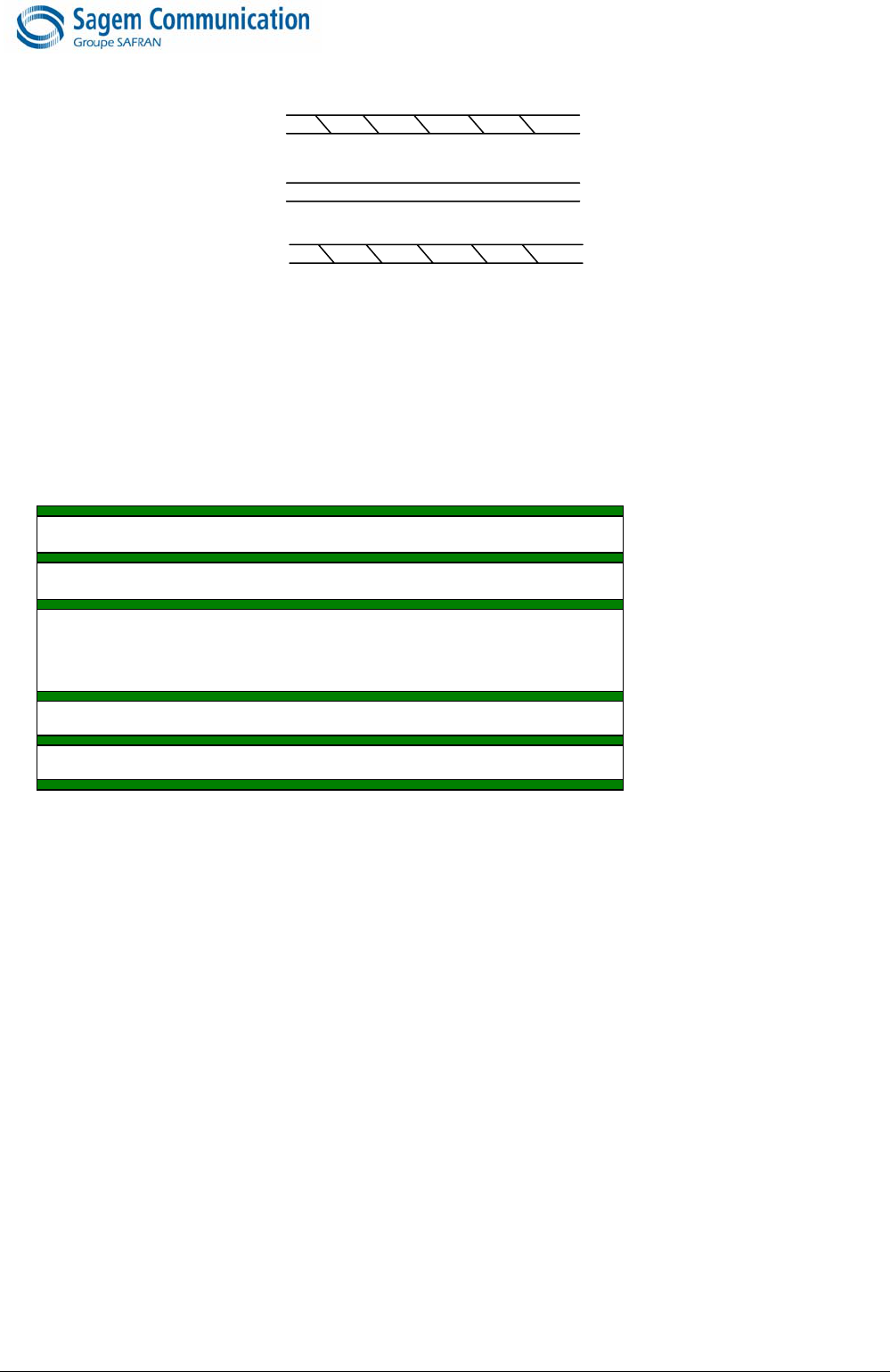
9.2 Example of layout for main board
The layout given hereafter is only for reference for a typical modem application, 6 layers are necessary.
Figure 33
6 layers Stack up example
For PDA application using processor, memories (RAM & flash), Audio codec, MO300, and other accessories, at
least 8 layers may be necessary for a correct and safe layout.
HSMICP
GND
GND
Layer n
Layer n+1
Layer n-1
Layer 1: Components (MO300)
Layer 2: bus
Layer 3: Power supplies
Layer 4: complete GND layer
Layer 5: Audio, clocks,
sensitive signals
Layer 6: GND, connectors
page 40/46
Note d’étude / Technical document : URD1 – 5625.1 – 006 / 69796 Edition 03
Document Sagem Communication Reproduction et divulgation interdites
Sagem Communication document. Reproduction and disclosure prohibited
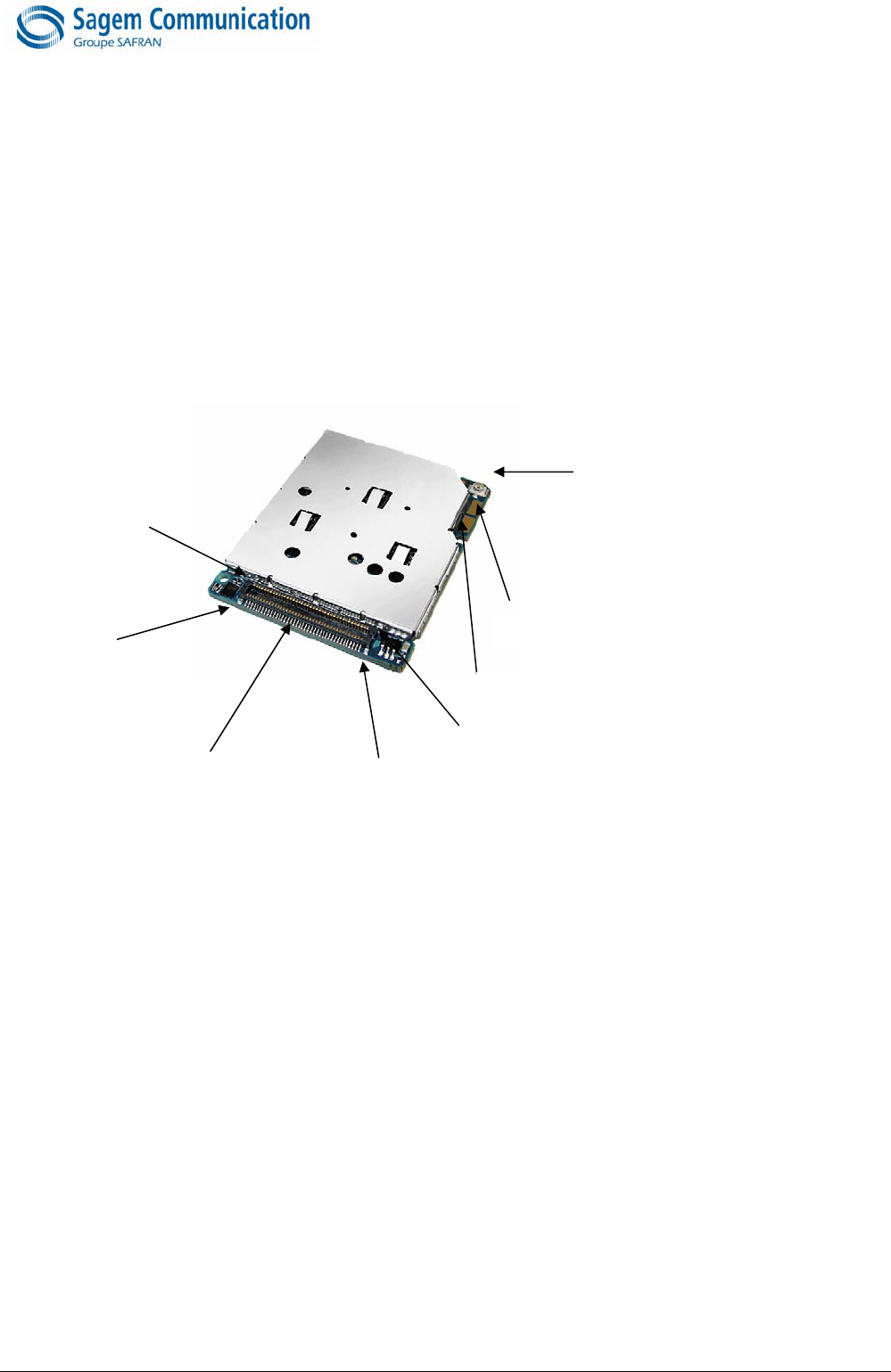
10 Mechanical integration
The different points in this part deal with the mechanical specifications to ensure a correct integration of the
module MO300. The constraints are about the connections (characteristics and layouts) and assembly of the
module inside any housing.
10.1 External connections presentation
There are 2 connections on the MO300 :
• The connection to the 80 signals : through a Molex Board to Board connector
• The connection to the radio ! through a Hirose coaxial connection and a range connection
Figure 35
MO300 connections
10.2 Connection constraints
10.2.1 Board to board connection
The Molex board to board connector is a 80 signals connection.
The plug is mounted on the MO300 board and the receptacle should be mounted on the main board (which the
module is connected to).
Molex Board to Board
80 pins connector
Ground area
Pad for antenna connection
Hirose coaxial connector
Pin 1
Pin 80
Pin 41
Pin 40
page 41/46
Note d’étude / Technical document : URD1 – 5625.1 – 006 / 69796 Edition 03
Document Sagem Communication Reproduction et divulgation interdites
Sagem Communication document. Reproduction and disclosure prohibited
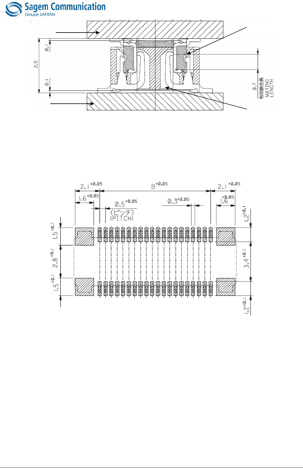
Figure 36
Board to board connection
To ensure a good soldering process for the receptacle on the main board, respect the layout specification
following (dimension in mm).
Figure 37
Recommended layout for board to board receptacle
10.2.2 Antenna connection
There are two possibilities to connect the antenna signal to the main board :
• The Hirose coaxial connection : a receptacle is mounted on the MO300, an other receptacle (the same
Hirose reference) should be mounted on the main board. The connection should be realised by a
plug/unplug cable.
• A contact plate connection
10.3 Warning related to the use of metallic housings
Metal particles presence in the mechanical disturbs strongly the radio performance of the module. For example,
the minimum sensitivities levels are not guarantied in case of such use. Moreover, Sagem does not recommend
to have metallic particles especially in the antenna area.
MO300 board
Main board
Rece
p
tacle
Plu
g

page 42/46
Note d’étude / Technical document : URD1 – 5625.1 – 006 / 69796 Edition 03
Document Sagem Communication Reproduction et divulgation interdites
Sagem Communication document. Reproduction and disclosure prohibited
11 Summary of integration
On the following pages, you will find a sum-up of the different connectors which are assembled in the module
MO300. Their references are mentioned and their specifications are available at the end of this document.
11.1 Annexe: Molex Board to Board connector
Dimensions and references:
Pin Number References
80 MOLEX 54150-0878
Sagem reference : 189576119
Dimension A B C
mm 23.9 19.5 20.5
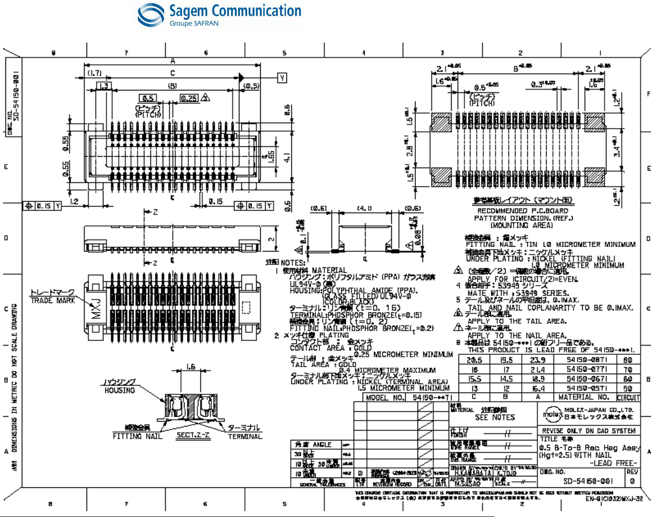
page 43/46
Note d’étude / Technical document : URD1 – 5625.1 – 006 / 69796 Edition 03
Document Sagem Communication Reproduction et divulgation interdites
Sagem Communication document. Reproduction and disclosure prohibited
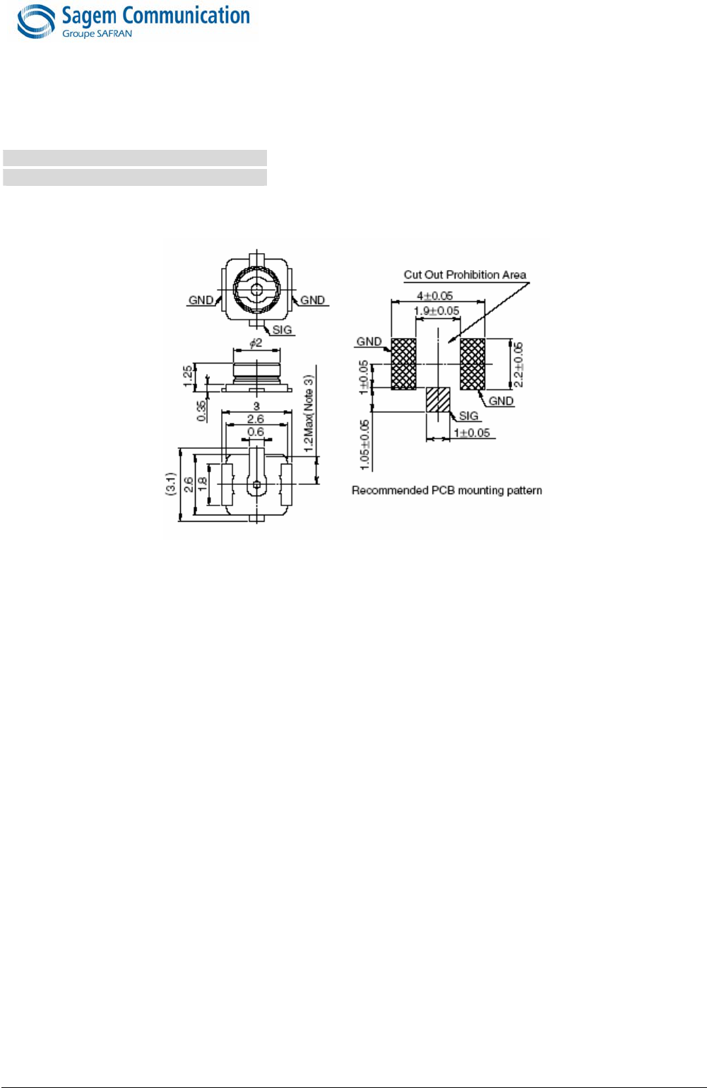
page 44/46
Note d’étude / Technical document : URD1 – 5625.1 – 006 / 69796 Edition 03
Document Sagem Communication Reproduction et divulgation interdites
Sagem Communication document. Reproduction and disclosure prohibited
11.2 Annexe: Hirose coaxial connector
Reference
HIROSE U.FL-R-SMT-1 (10)
Sagem reference 189492503
page 45/46
Note d’étude / Technical document : URD1 – 5625.1 – 006 / 69796 Edition 03
Document Sagem Communication Reproduction et divulgation interdites
Sagem Communication document. Reproduction and disclosure prohibited
11.3 Annexe: Spring contact for antenna
Figure 38
layer allocation for a 6 layers circuit

page 46/46
Note d’étude / Technical document : URD1 – 5625.1 – 006 / 69796 Edition 03
Document Sagem Communication Reproduction et divulgation interdites
Sagem Communication document. Reproduction and disclosure prohibited
12 LABEL
The MO300 module is labelled with its own FCC ID (VW3MO300QBM) on its bottom side.
When the module is installed in customer’s product, the FCC ID label on the module will not be visible. To avoid
this case, an exterior label must be stuck on the surface of customer’s product signally to indicate the FCC ID of
the enclosed module. This label can use wording such as the following: “Contains Transmitter module FCC ID:
VW3MO300QBM” or “Contains FCC ID: VW3MO300QBM”.
-o-
END OF DOCUMENT
-o-