ST Microelectronics S R L SPBTLERF SPBTLE-RF Bluetooth Low Energy Module User Manual SPBT2632C1A AT
ST Microelectronics S.R.L. SPBTLE-RF Bluetooth Low Energy Module SPBT2632C1A AT
UserManual.wiki
>
ST Microelectronics S R L
>
SPBTLERF User Manual
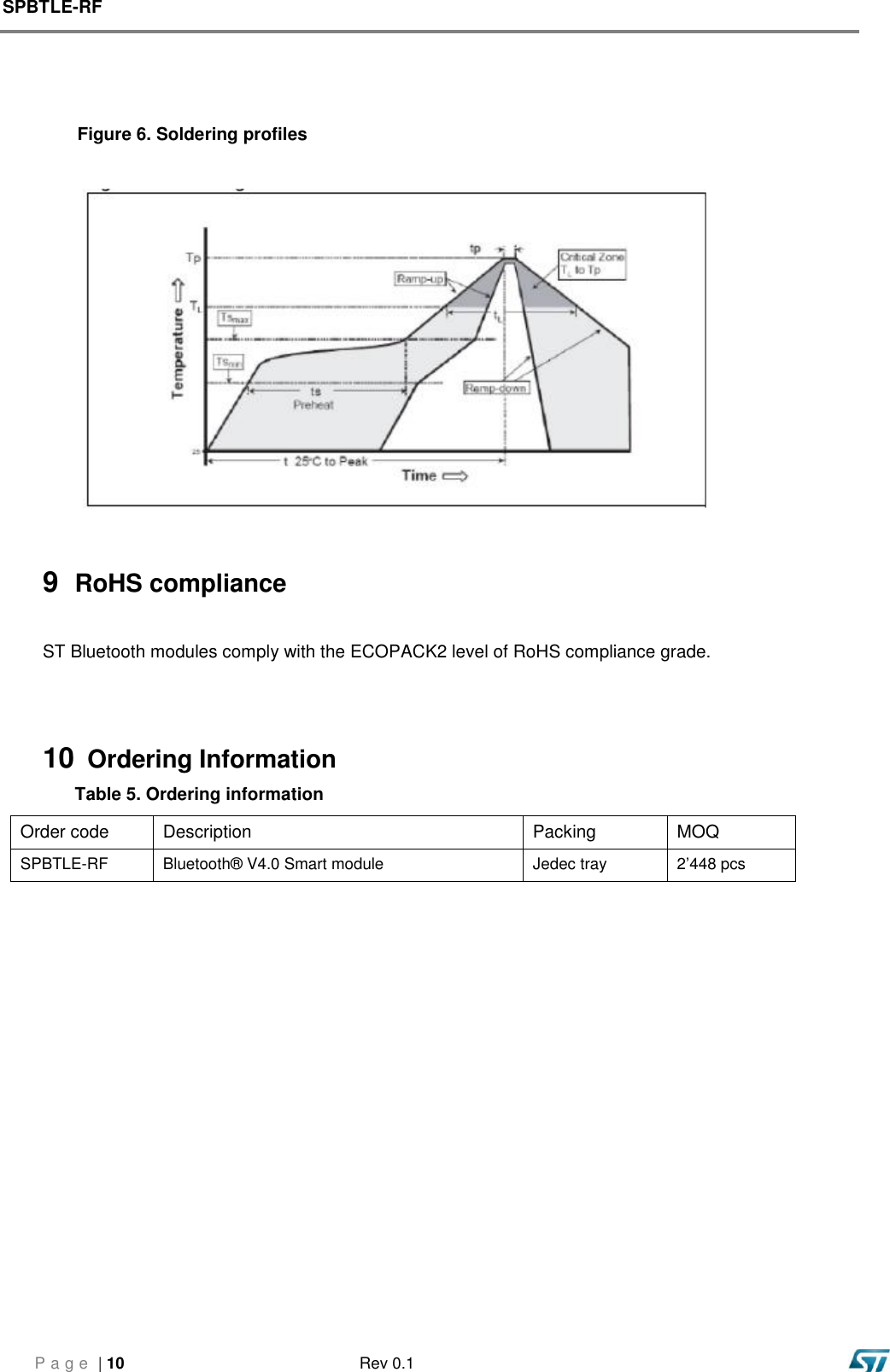
Datasheet
Navigation menu
Upload a User Manual
Namespaces
Wiki Guide
HTML
PDF
Info
Views
User Manual
Discussion / Help
Navigation