ST Microelectronics S R L SPBTLERF SPBTLE-RF Bluetooth Low Energy Module User Manual SPBT2632C1A AT
ST Microelectronics S.R.L. SPBTLE-RF Bluetooth Low Energy Module SPBT2632C1A AT
Datasheet
SPBTLE-RF
Bluetooth® V4.1 Smart module
Product preview
Jan 2015 - rev 0.1
This is preliminary information on a new product now in development or undergoing evaluation. Details are
subject to change without notice. www.st.com www.st.com
Features
Bluetooth Radio
- Bluetooth specification v4.1 compliant
- Master and slave Smart Bluetooth network
processor module
- Embedded Bluetooth low energy protocol
stack: GAP, GATT, SM, L2CAP, LL,
RF-PHY
- Bluetooth low energy profiles provided
separately
- Operating temperature range: -40°C to
85°C
Host Interface
- SPI, IRQ, and RESET
Antenna on board
CE, FCC, IC qualified
BQE certified
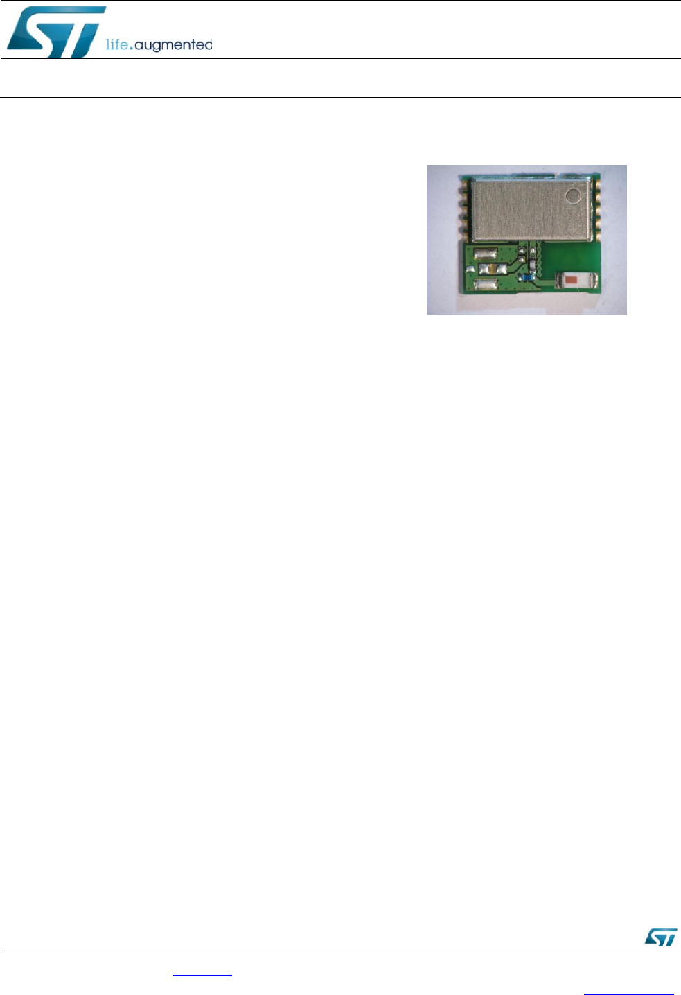
Preliminary module picture
11.5 mm x 13.5 mm x 2.0 mm

SPBTLE-RF
P a g e | 2 Rev 0.1
1 Description
The SPBTLE-RF is an easy to use Bluetooth® module, compliant with Bluetooth® v4.1.
The module provides a complete RF platform in a tiny form factor.
The SPBTLE-RF enables wireless connectivity into electronic devices, not requiring any
RF experience or expertise for integration into the final product. The SPBTLE-RF
module, being a certified solution, optimizes the time to market of the final applications.
The module has been designed for maximum performance in a minimal space.
Optimized design allows the integration of a complete working Bluetooth® modem in the
minimum possible size. Module interface is SPI serial interface.
2 Applications
Watches
Fitness, wellness and sports
Consumer medical
Security/proximity
Remote control
Home and industrial automation
Assisted living
Mobile phone peripherals
PC peripherals
SPBTLE-RF
Rev 0.1 P a g e | 3
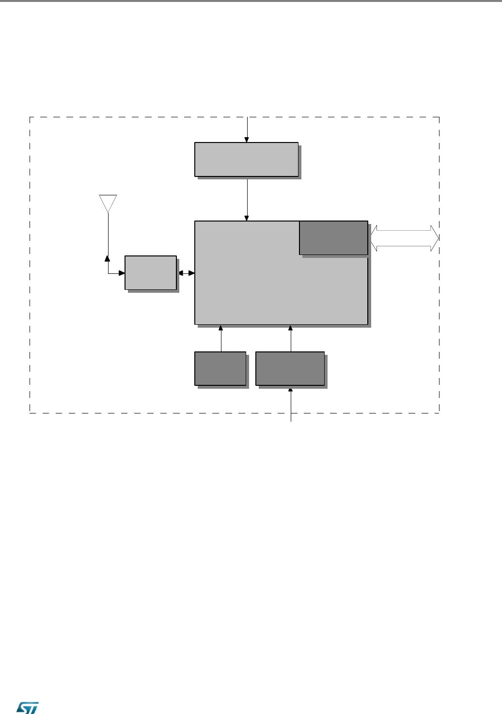
3 Block Diagram
Figure 1. HW block diagram
RF antenna
Battery or External Supply
SPI LINE
BLUETOOTH
BLUENRG
Host Controller
interface
External LPO
(32.768 kHz)
32.768 kHz
BLUETOOTH L.E.. 2014 Module
Crystal
32 MHz
clock
SUPPLY FILTER
Bead Ferrite
RF
BALUN
+ Filter
Internal / Ext.
32.768 kHz
clock
INTERNAL 2.45 GHz
OPTIONAL PIN FUNCTION
SPBTLE-RF
P a g e | 4 Rev 0.1
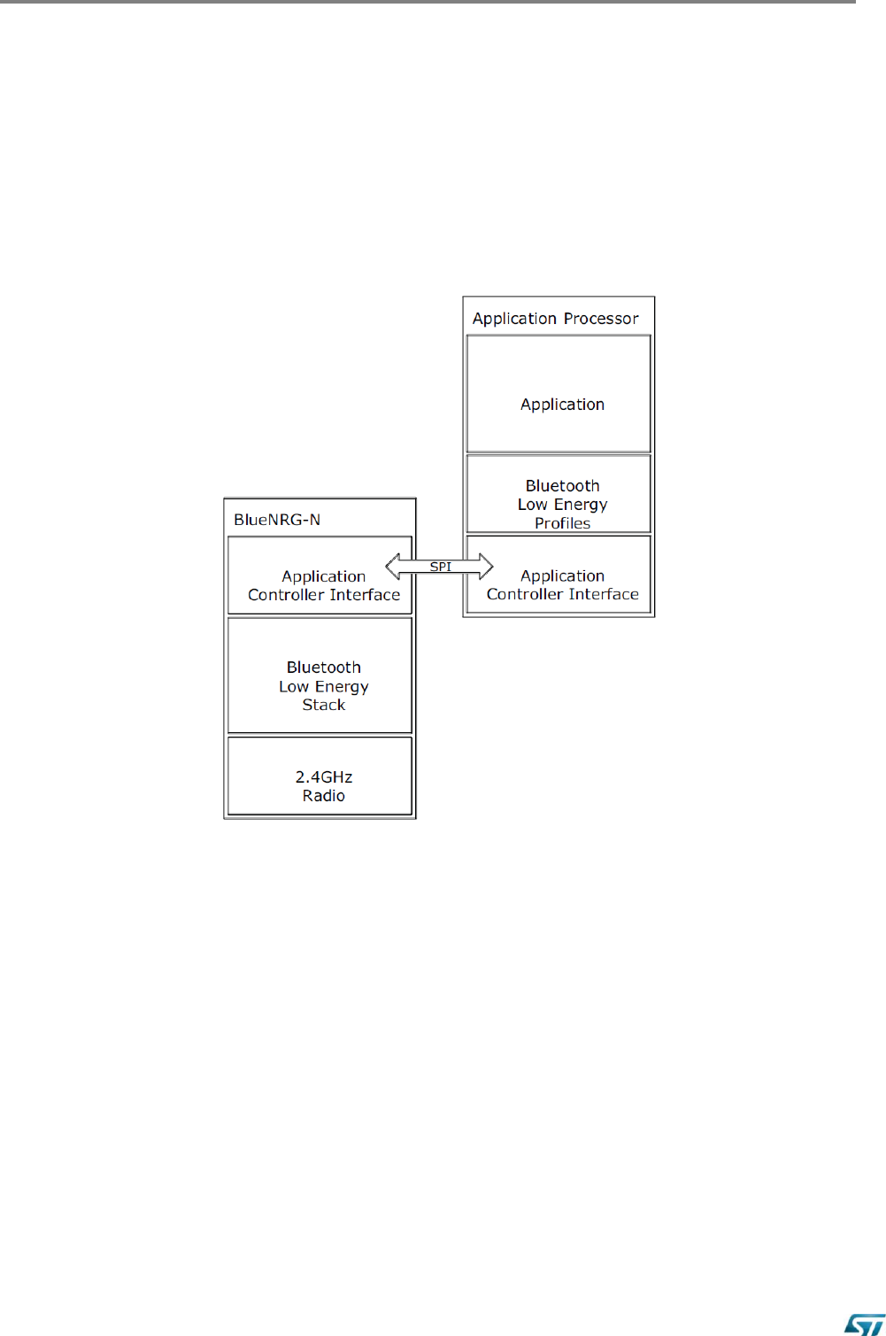
4 Software Architecture
Bluetooth Firmware implementation
Figure 2. SPBTLE-RF Application Block Diagaram
SPBTLE-RF
Rev 0.1 P a g e | 5
5 Hardware Specifications
General Conditions (VIN= 2.2V and 25°C)
5.1 Absolute Maximum Ratings
Table 1. Absolute maximum rating
Rating
Min
Typical
Max
Unit
Storage temperature range
-40
-
+85
°C
Supply voltage, VIN
-0.3
-
+ 3.9
Volts
I/O pin Voltage
(VIO five-volt tolerant pin)
-0.3
-
+ 3.9
Volts
RF saturation input power
-
8
-
dBm
5.2 Recommended Operating Conditions
Table 2. Recommended operating conditions
Rating
Min
Typical
Max
Unit
Operating Temperature Range
-40
-
85
°C
Supply Voltage VIN
2.0
3.3
3.6
Volts
Signals & I/O Pin Voltage
(according Supply Voltage)
2.0
-
3.6
Volts
RF Frequency
2402
-
2480
MHz
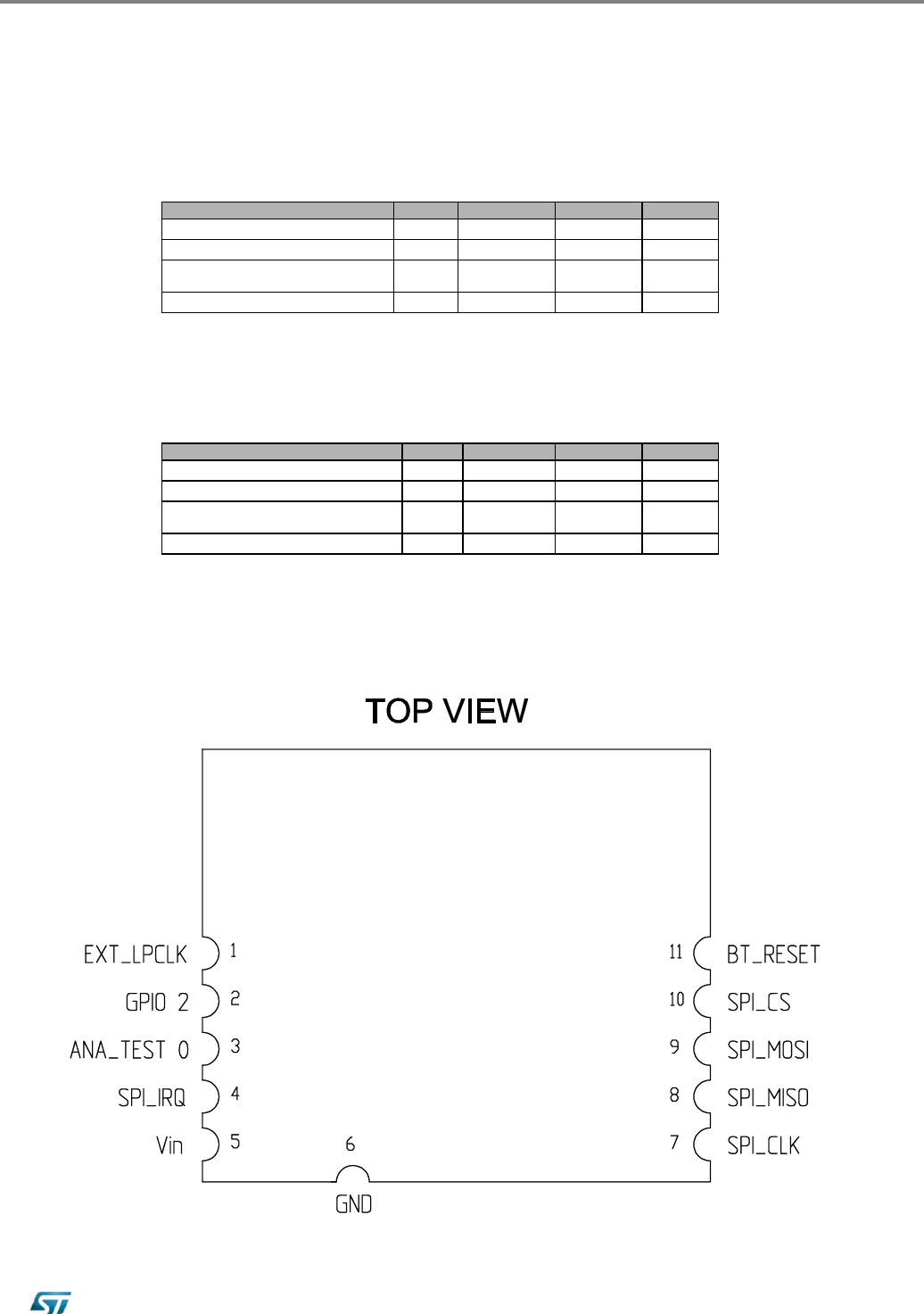
5.3 Pin assignement
Figure 3. Pin connection

SPBTLE-RF
P a g e | 6 Rev 0.1
Table 3. Pin Assignement
Name
Type
Pin #
Description
ALT Function
V max. Tolerant
Initial State
SPI Interface
SPI_IRQ
O
4
SPI IRQ(SLAVE has data for MASTER)
Vin
SPI_CLK
I
7
SPI CLOCK (Max. 8 MHz)
Vin
SPI_MISO
O
8
SPI MISO (MASTER in / SLAVE out)
Vin
SPI_MOSI
I
9
SPI MOSI (MASTER out SLAVE in)
Vin
SPI_CS
I
10
SPI “Chip Select” (SPI slave select)
Vin
Power and Ground
Vin
5
Vin
(2.0V + 3.6V max.)
GND
6
GND
Reset
BT_RESET
I
11
Reset input (active low < 0.35 Vin)
(2.0V + 3.6V max.).
LPO
EXT_LPCLK
I
1
Not connected / Optional pin function
(2.0V + Vin max.).
GPIO2
I/O
2
Not connected
ANA TEST 0
I
3
Not connected
SPBTLE-RF
Rev 0.1 P a g e | 7
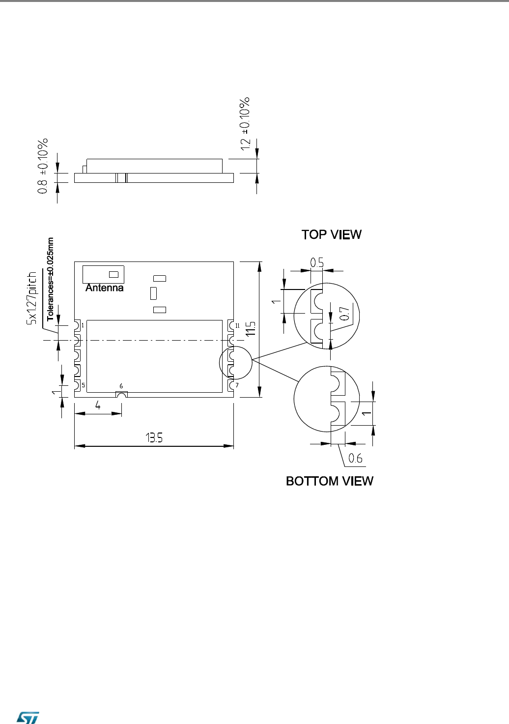
6 Mechanical dimensions
Figure 4. Mechanical dimensions
SPBTLE-RF
P a g e | 8 Rev 0.1
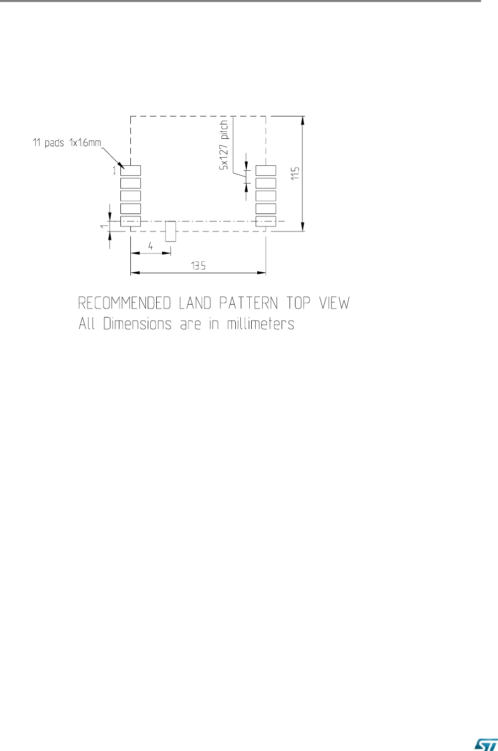
Figure 5. Recommend land pattern top view
SPBTLE-RF
Rev 1.0 P a g e | 9
7 Hardware design
SPBTLE-RF module supports SPI hardware interfaces.
Notes
All unused pins should be left floating; do not ground.
All GND pins must be well grounded.
The area around the module should be free of any ground planes, power planes, trace
routings, or metal for 6 mm from the module antenna position, in all directions.
Traces should not be routed underneath the module.
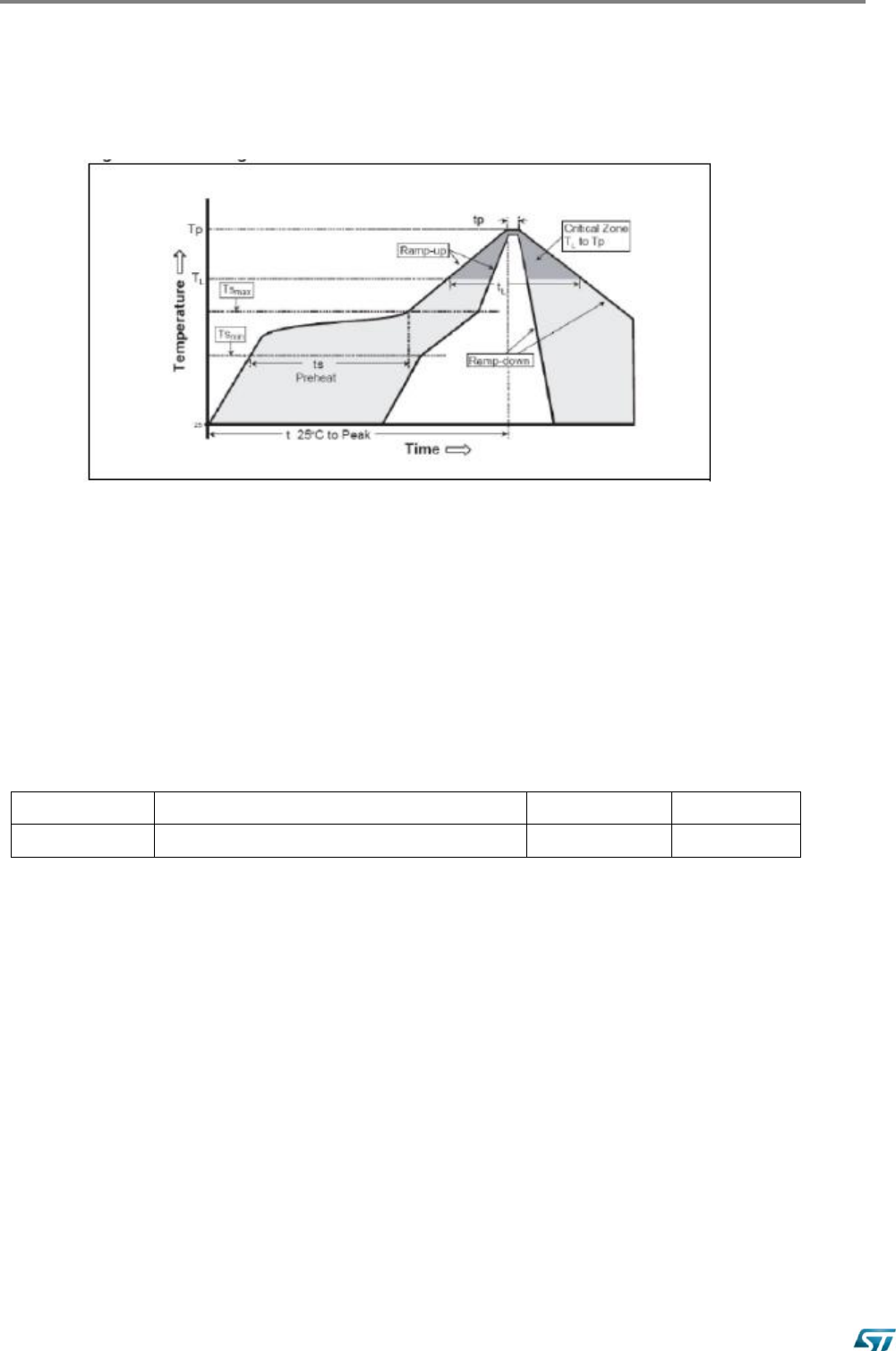
8 Reflow soldering
The SPBTLE-RF is a high temperature strength surface mount Bluetooth® module supplied on a 11
pin, 4-layer PCB. The final assembly recommended reflow profiles are indicated here below.
Soldering phase has to be executed with care: in order to avoid undesired melting phenomenon,
particular attention has to be taken on the set up of the peak temperature.
Here following some suggestions for the temperature profile based on IPC/JEDEC J-STD-020C,
July 2004 recommendations.
Table 4. Soldering
Profile feature
PB-free assembly
Average ramp up rate (TSMAX to Tp)
3°C/ sec max
Preheat
Temperature min (TS mn)
Temperature max (TS max)
Time (tS min to tS max) (tS)
150 °C
200 °C
60-100 sec
Time maintained above:
Temperature TL
Time tL
217 °C
60-70 sec
Peak temperature (TP)
240 + 0 °C
Time within 5 °C of actual peak temperature (TP)
10-20 sec
Ramp down rate
6 °C/sec
Time from 25 °C to peak temperature
8 minutes max
SPBTLE-RF
P a g e | 10 Rev 0.1
Figure 6. Soldering profiles
9 RoHS compliance
ST Bluetooth modules comply with the ECOPACK2 level of RoHS compliance grade.
10 Ordering Information
Table 5. Ordering information
Order code
Description
Packing
MOQ
SPBTLE-RF
Bluetooth® V4.0 Smart module
Jedec tray
2’448 pcs

SPBTLE-RF
Rev 1.0 P a g e | 11
11 Traceability
Each module is univocally identified by serial number stored in a 2D data matrix laser
marked on the bottom side of the module itself.
The serial number has the following format:
WW YY D FF NNN
where
WW = week
YY = year
D = product ID family
FF = production panel coordinate identification
NNN = progressive serial number.
Each module bulk is identified by a bulk ID.
BULK ID and module 2D data matrix are linked by a reciprocal traceability link.
The module 2D data matrix traces the lot number of any raw material used.

SPBTLE-RF
P a g e | 12 Rev 0.1
12 Regulatory compliance
12.1 FCC certification
This module has been tested and found to comply with the FCC part 15 rules. These
limits are designed to provide reasonable protection against harmful interference in
approved installations. This equipment generates, uses, and can radiate radio
frequency energy and, if not installed and used in accordance with the instructions,
may cause harmful interference to radio communications.
However, there is no guarantee that interference may not occur in a particular
installation.
This device complies with part 15 of the FCC rules. Operation is subject to the following
two conditions: (1) This device may not cause harmful interference, and (2) this device
must accept any interference received, including interference that may cause
undesired operation.
Modifications or changes to this equipment not expressly approved by
STMicroelectronics may render void the user's authority to operate this equipment.
Modular approval
FCC ID: S9NSPBTLERF
In accordance with FCC part 15, the SPBTLE-RF is listed as a modular transmitter
device.
This module is evaluated for stand-alone use only. Finished products incorporating
multiple transmitters must comply with colocation and RF exposure requirements in
accordance with FCC multi-transmitter product procedures. Collocated transmitters
operating in portable RF Exposure conditions (e.g. <20cm from persons including but
not limited to body worn and hand held devices) may require separate approval.
Labeling instructions
When integrating the SPBTLE-RF into the final product, the OEM must ensure that the
FCC labeling requirements are satisfied. A statement must be included on the exterior
of the final product which indicates the product includes a certified module. The label
should state the following (or similar wording that conveys the same meaning):
Contains FCC ID: S9NSPBTLERF
OR This product contains FCC ID: S9NSPBTLERF
The OEM must include the following statements on the exterior of the final product
unless the product is too small (e.g. less than 4 x 4 inches):
This device complies with Part 15 of the FCC Rules. Operation is subject to the
following two conditions: (1) this device may not cause harmful interference, and (2)
this device must accept any interference received, including any interference that may
cause undesired operation.

SPBTLE-RF
Rev 1.0 P a g e | 13
Product manual instructions
This section applies to OEM final products containing the SPBTLE-RF module, subject
to FCC compliance. The final product manual must contain the following statement (or
a similar statement that conveys the same meaning):
WARNING: Changes or modifications not expressly approved by the party
responsible for compliance could void the user’s authority to operate the equipment.
(Part. 15.21)
In the case where an OEM seeks Class B (residential) limits for the final product, the
following statement must be included in the final product manual:
NOTE: This equipment has been tested and found to comply with the limits for a Class
B digital device, pursuant to part 15 of the FCC Rules. These limits are designed to
provide reasonable protection against harmful interference in a residential installation.
This equipment generates, uses and can radiate radio frequency energy and, if not
installed and used in accordance with the instructions, may cause harmful interference
to radio communications. However, there is no guarantee that interference will not
occur in a particular installation. If this equipment does cause harmful interference to
radio or television reception, which can be determined by turning the equipment off and
on, the user is encouraged to try to correct the interference by one or more of the
following measures:
Reorient or relocate the receiving antenna.
Increase the separation between the equipment and receiver.
Connect the equipment into an outlet on a circuit different from that to which
the receiver is connected.
Consult the dealer or an experienced radio/TV technician for help.
In the case where an OEM seeks the lesser category of a Class A digital device for the
final product, the following statement must be included in the final product manual:
NOTE: This equipment has been tested and found to comply with the limits for a Class
A digital device, pursuant to part 15 of the FCC Rules. These limits are designed to
provide reasonable protection against harmful interference when the equipment is
operated in a commercial environment. This equipment generates, uses, and can
radiate radio frequency energy and, if not installed and used in accordance with the
instruction manual, may cause harmful interference to radio communications.
Operation of this equipment in a residential area is likely to cause harmful interference
in which case the user will be required to correct the interference at his expense.

SPBTLE-RF
P a g e | 14 Rev 0.1
12.2 IC certification
The SPBTLE-RF module has been tested and found compliant with the IC RSS-210 rules.
These limits are designed to provide reasonable protection against harmful interference in
approved installations. This equipment generates, uses, and can radiate radio frequency
energy and, if not installed and used in accordance with the instructions, may cause harmful
interference to radio communications.
However, there is no guarantee that interference may not occur in a particular installation.
This device complies with RSS-210 of the IC rules. Operation is subject to the following two
conditions: (1) this device may not cause harmful interference, and (2) this device must accept
any interference received, including interference that may cause undesired operation.
Modifications or changes to this equipment not expressly approved by STMicroelectronics may
render void the user's authority to operate this equipment.
Modular approval
IC: 8976C-SPBTLERF
In accordance with IC RSS-210, the SPBTLE-RF is listed as a modular transmitter device.
This module is evaluated for stand-alone use only. Finished products incorporating multiple
transmitters must comply with colocation and RF exposure requirements in accordance with IC
multi-transmitter product procedures. Collocated transmitters operating in portable RF
Exposure conditions (e.g. <20cm from persons including but not limited to body worn and hand
held devices) may require separate approval.
12.2.1 Labeling instructions
When integrating the SPBTLE-RF into the final product, the OEM must ensure that the IC
labeling requirements are satisfied. A statement must be included on the exterior of the final
product which indicates that the product includes a certified module. The label should state the
following (or similar wording that conveys the same meaning):
Contains IC: 8976C-SPBTLERF
OR This product contains IC: 8976C-SPBTLERF
The OEM must include the following statements on the exterior of the final product unless the
product is too small (e.g. less than 4 x 4 inches):
This device complies with RSS-210 of the IC Rules. Operation is subject to the following two
conditions: (1) this device may not cause harmful interference, and (2) this device must accept
any interference received, including any interference that may cause undesired operation.
12.2.2 Product manual instructions
This section applies to OEM final products containing the SPBTLE-RF module, subject to IC
compliance. The final product manual must contain the following statement (or a similar
statement that conveys the same meaning):
WARNING: Changes or modifications not expressly approved by the party responsible for
compliance could void the user’s authority to operate the equipment. (RSS-210)

SPBTLE-RF
Rev 1.0 P a g e | 15
In the case where an OEM seeks Class B (residential) limits for the final product, the following
statement must be included in the final product manual:
NOTE: This equipment has been tested and found to comply with the limits for a Class B digital
device, pursuant to RSS-210 of the IC Rules. These limits are designed to provide reasonable
protection against harmful interference in a residential installation. This equipment generates,
uses and can radiate radio frequency energy and, if not installed and used in accordance with
the instructions, may cause harmful interference to radio communications. However, there is no
guarantee that interference will not occur in a particular installation. If this equipment does
cause harmful interference to radio or television reception, which can be determined by turning
the equipment off and on, the user is encouraged to try to correct the interference by one or
more of the following measures:
Reorient or relocate the receiving antenna.
Increase the separation between the equipment and receiver.
Connect the equipment into an outlet on a circuit different from that to which the
receiver is connected.
Consult the dealer or an experienced radio/TV technician for help.
In the case where an OEM seeks the lesser category of a Class A digital device for the final
product, the following statement must be included in the final product manual:
NOTE: This equipment has been tested and found to comply with the limits for a Class A digital
device, pursuant to RSS-210 of the IC Rules. These limits are designed to provide reasonable
protection against harmful interference when the equipment is operated in a commercial
environment. This equipment generates, uses, and can radiate radio frequency energy and, if
not installed and used in accordance with the instruction manual, may cause harmful
interference to radio communications. Operation of this equipment in a residential area is likely
to cause harmful interference in which case the user will be required to correct the interference
at his expense.
SPBTLE-RF
P a g e | 16 Rev 0.1
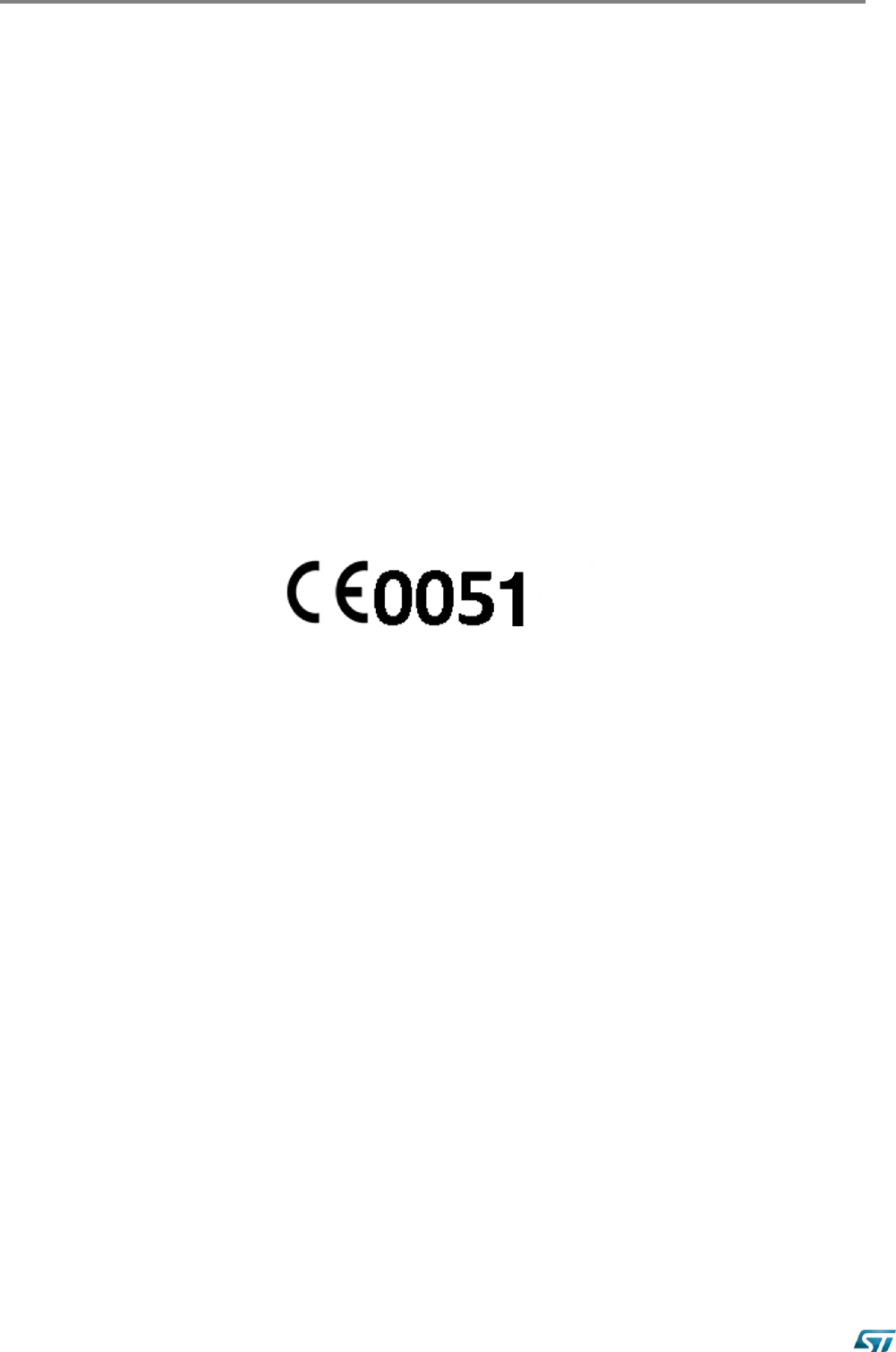
CE certification for SPBTLE-RF module
The SPBTLE-RF module has been certified according to the following standards:
EN 60950-1:2006 + A11:2009 + A12:2011 + A1:2010 + A2:2013 + AC:2011
ETSI EN 301 489-1 V1.9.2:2011
ETSI EN 301 489-17 V2.2.1
ETSI EN 300 328 V1.8.1 :2012
ETSI EN 300 328 V1.9.1 (2015)
EN62479 :2010
The module is CE certified:

SPBTLE-RF
Rev 1.0 P a g e | 17
Please Read Carefully:
Information in this document is provided solely in connection with ST products. STMicroelectronics NV and its subsidiaries (“ST”) reserve
the right to make changes, corrections, modifications or improvements, to this document, and the products and services described herein
at any time, without notice.
All ST products are sold pursuant to ST’s terms and conditions of sale.
Purchasers are solely responsible for the choice, selection and use of the ST products and services described herein, and ST assumes
no liability whatsoever relating to the choice, selection or use of the ST products and services described herein.
No license, express or implied, by estoppel or otherwise, to any intellectual property rights is granted under this document. If any part of
this document refers to any third party products or services it shall not be deemed a license grant by ST for the use of such third party
products or services, or any intellectual property contained therein or considered as a warranty covering the use in any manner
whatsoever of such third party products or services or any intellectual property contained therein.
UNLESS OTHERWISE SET FORTH IN ST’S TERMS AND CONDITIONS OF SALE ST DISCLAIMS ANY EXPRESS OR IMPLIED
WARRANTY WITH RESPECT TO THE USE AND/OR SALE OF ST PRODUCTS INCLUDING WITHOUT LIMITATION IMPLIED
WARRANTIES OF MERCHANTABILITY, FITNESS FOR A PARTICULAR PURPOSE (AND THEIR EQUIVALENTS UNDER THE
LAWS OF ANY JURISDICTION), OR INFRINGEMENT OF ANY PATENT, COPYRIGHT OR OTHER INTELLECTUAL PROPERTY
RIGHT.
ST PRODUCTS ARE NOT DESIGNED OR AUTHORIZED FOR USE IN: (A) SAFETY CRITICAL APPLICATIONS SUCH AS LIFE
SUPPORTING, ACTIVE IMPLANTED DEVICES OR SYSTEMS WITH PRODUCT FUNCTIONAL SAFETY REQUIREMENTS; (B)
AERONAUTIC APPLICATIONS; (C) AUTOMOTIVE APPLICATIONS OR ENVIRONMENTS, AND/OR (D) AEROSPACE
APPLICATIONS OR ENVIRONMENTS. WHERE ST PRODUCTS ARE NOT DESIGNED FOR SUCH USE, THE PURCHASER SHALL
USE PRODUCTS AT PURCHASER’S SOLE RISK, EVEN IF ST HAS BEEN INFORMED IN WRITING OF SUCH USAGE, UNLESS A
PRODUCT IS EXPRESSLY DESIGNATED BY ST AS BEING INTENDED FOR “AUTOMOTIVE, AUTOMOTIVE SAFETY OR
MEDICAL” INDUSTRY DOMAINS ACCORDING TO ST PRODUCT DESIGN SPECIFICATIONS. PRODUCTS FORMALLY ESCC,
QML OR JAN QUALIFIED ARE DEEMED SUITABLE FOR USE IN AEROSPACE BY THE CORRESPONDING GOVERNMENTAL
AGENCY.
Resale of ST products with provisions different from the statements and/or technical features set forth in this document shall immediately
void any warranty granted by ST for the ST product or service described herein and shall not create or extend in any manner whatsoever,
any liability of ST.
ST and the ST logo are trademarks or registered trademarks of ST in various countries.
Information in this document supersedes and replaces all information previously supplied.
The ST logo is a registered trademark of STMicroelectronics. All other names are the property of their respective owners.
© 2014 STMicroelectronics - All rights reserved
STMicroelectronics group of companies
Australia - Belgium - Brazil - Canada - China - Czech Republic - Finland - France - Germany - Hong Kong - India - Israel - Italy - Japan -
Malaysia - Malta - Morocco - Philippines - Singapore - Spain - Sweden - Switzerland - United Kingdom - United States of America
www.st.com