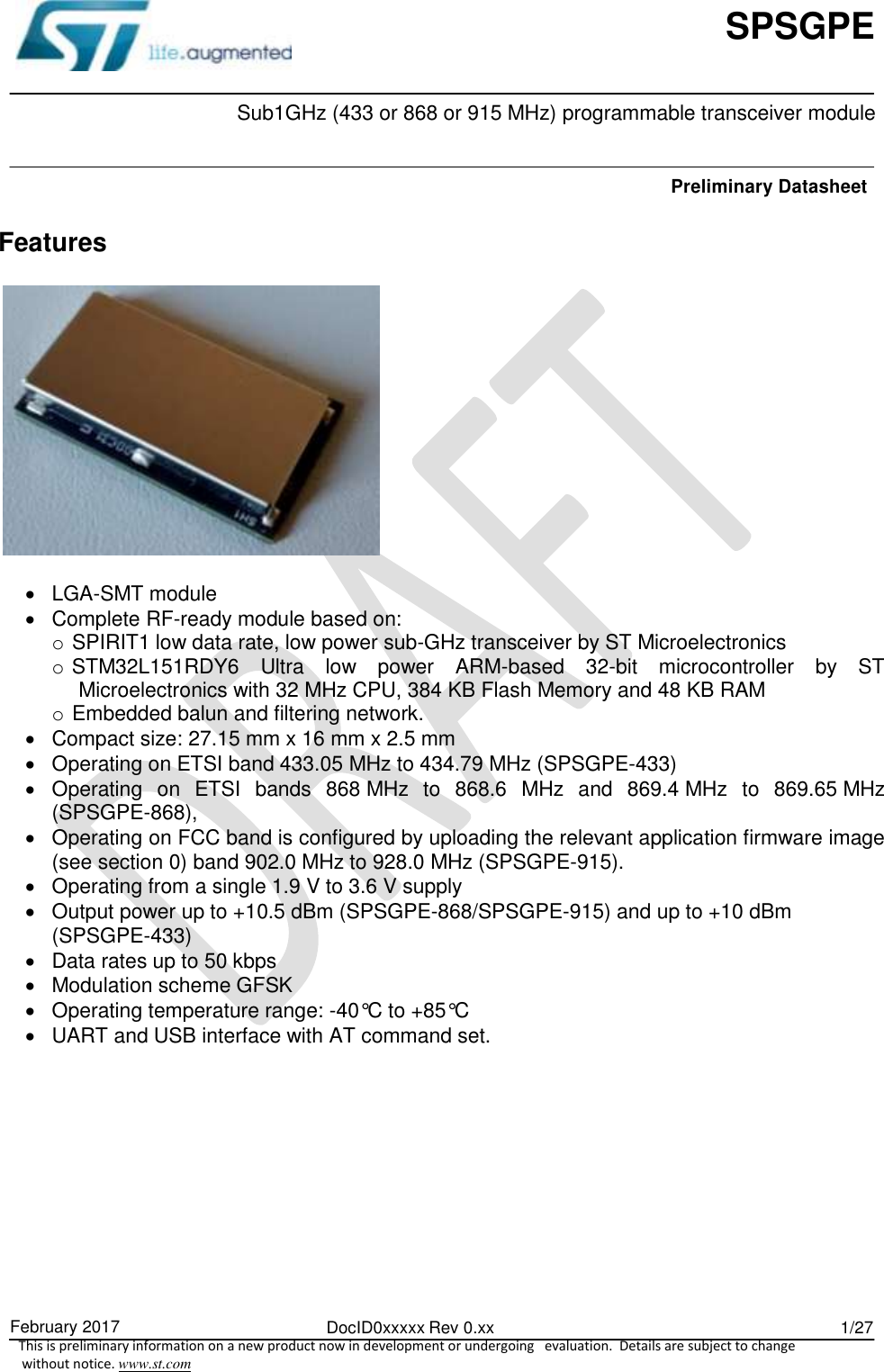
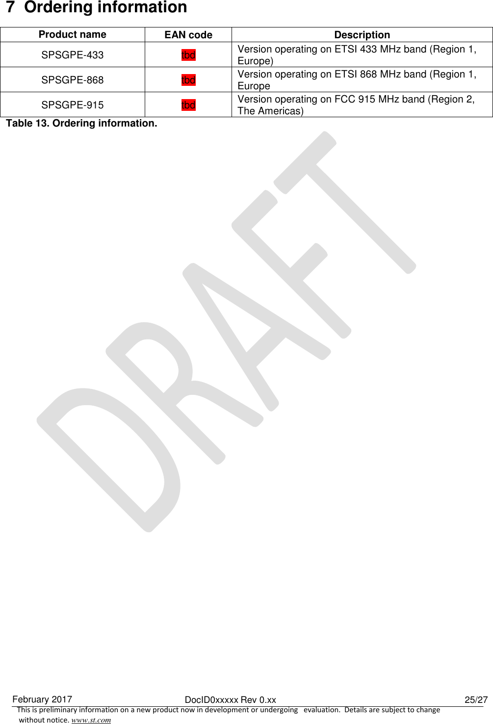
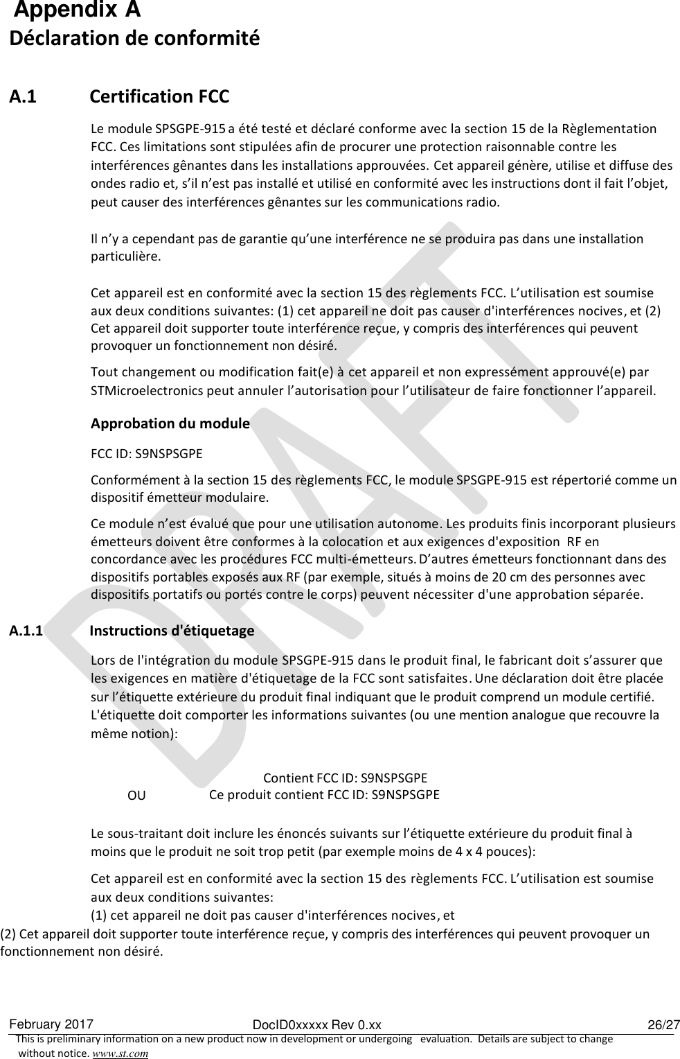
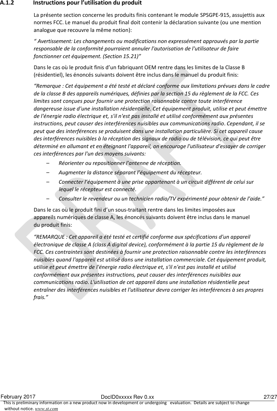
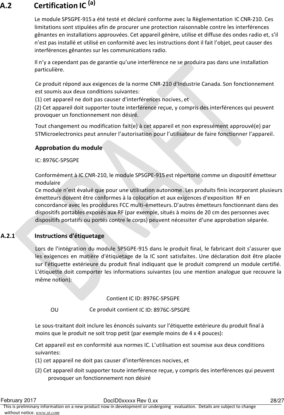
ST Microelectronics S R L SPSGPE SPSGPE-915 SubGiga Module User Manual
ST Microelectronics S.R.L. SPSGPE-915 SubGiga Module
UserManual.wiki
>
ST Microelectronics S R L
>
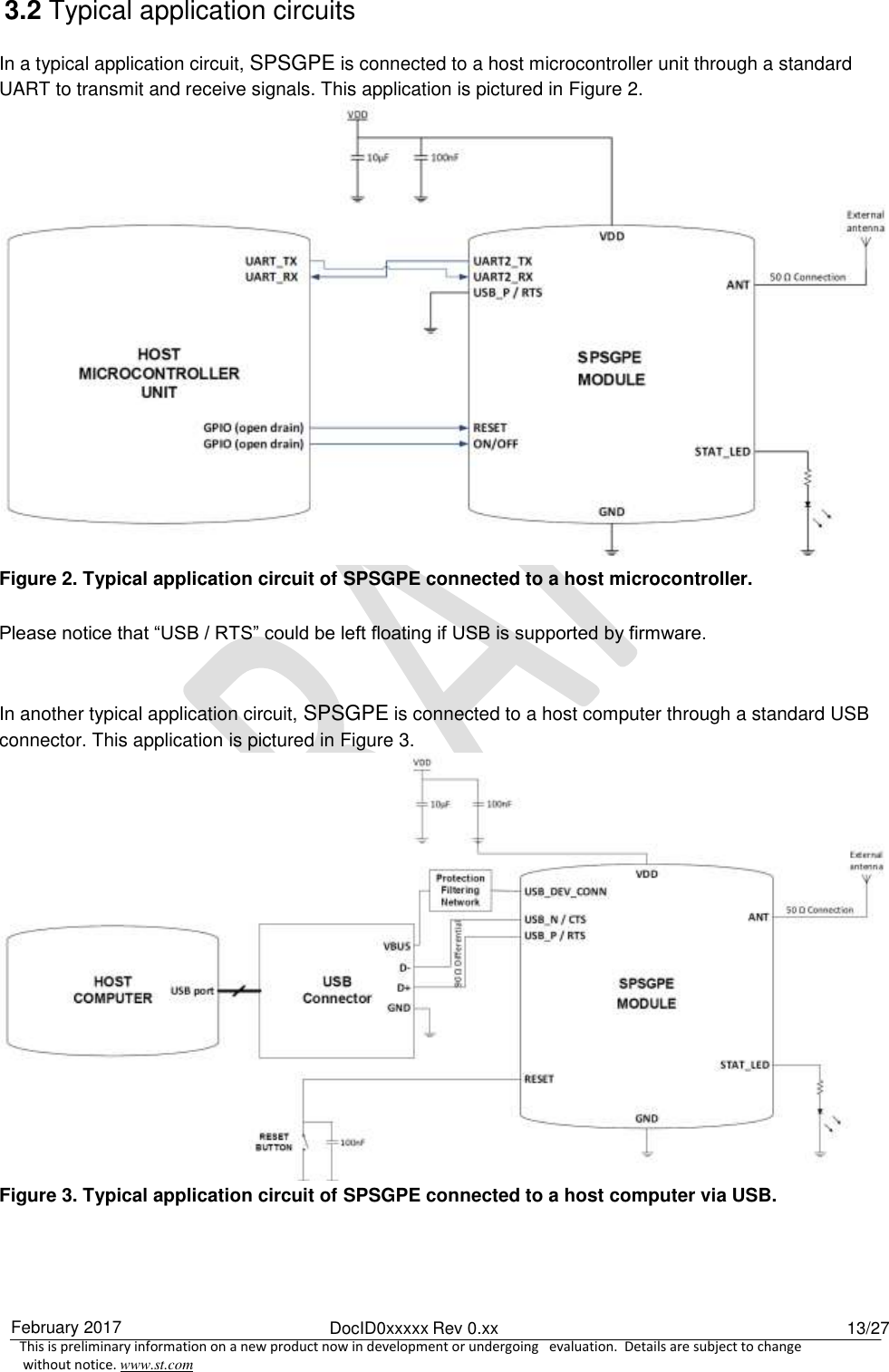
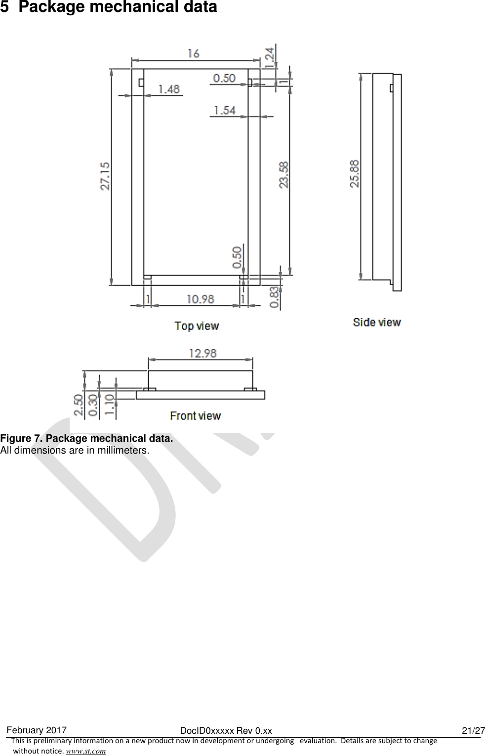
SPSGPE User Manual
User Manual
Navigation menu
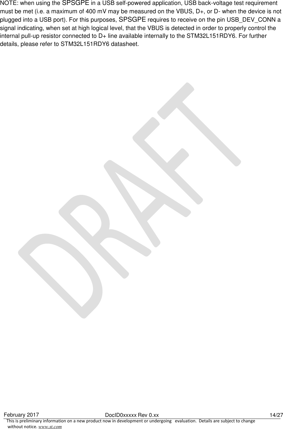
Upload a User Manual
Namespaces
Wiki Guide
HTML
PDF
Info
Views
User Manual
Discussion / Help
Navigation