ST Microelectronics S R L SPSGPE SPSGPE-915 SubGiga Module User Manual
ST Microelectronics S.R.L. SPSGPE-915 SubGiga Module
User Manual
February 2017 DocID0xxxxx Rev 0.xx 1/27
This is preliminary information on a new product now in development or undergoing evaluation. Details are subject to change
without notice. www.st.com
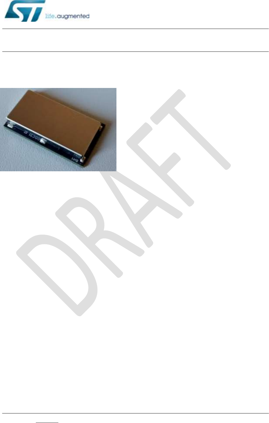
SPSGPE
Sub1GHz (433 or 868 or 915 MHz) programmable transceiver module
Preliminary Datasheet
Features
LGA-SMT module
Complete RF-ready module based on:
o SPIRIT1 low data rate, low power sub-GHz transceiver by ST Microelectronics
o STM32L151RDY6 Ultra low power ARM-based 32-bit microcontroller by ST
Microelectronics with 32 MHz CPU, 384 KB Flash Memory and 48 KB RAM
o Embedded balun and filtering network.
Compact size: 27.15 mm x 16 mm x 2.5 mm
Operating on ETSI band 433.05 MHz to 434.79 MHz (SPSGPE-433)
Operating on ETSI bands 868 MHz to 868.6 MHz and 869.4 MHz to 869.65 MHz
(SPSGPE-868),
Operating on FCC band is configured by uploading the relevant application firmware image
(see section 0) band 902.0 MHz to 928.0 MHz (SPSGPE-915).
Operating from a single 1.9 V to 3.6 V supply
Output power up to +10.5 dBm (SPSGPE-868/SPSGPE-915) and up to +10 dBm
(SPSGPE-433)
Data rates up to 50 kbps
Modulation scheme GFSK
Operating temperature range: -40°C to +85°C
UART and USB interface with AT command set.

List of tables
February 2017 DocID0xxxxx Rev 0.xx 2/27
This is preliminary information on a new product now in development or undergoing evaluation. Details are subject to change
without notice. www.st.com
Contents
1 Description .............................................................................................................................. 5
2 Hardware specifications........................................................................................................... 6
2.1 Recommended operating conditions .................................................................................. 6
2.2 Absolute maximum ratings ................................................................................................. 6
2.3 I/O operating specifications ................................................................................................ 6
2.4 Current consumption .......................................................................................................... 7
2.5 RF compliance limits .......................................................................................................... 7
2.6 RF sensitivity data .............................................................................................................. 8
2.7 Pin assignment ................................................................................................................... 9
2.8 Pin placement................................................................................................................... 10
2.9 Memory resources ............................................................................................................ 11
2.10 Hardware block diagram ............................................................................................... 11
3 Hardware design ................................................................................................................... 12
3.1 Pin usage ......................................................................................................................... 12
3.2 Typical application circuits ................................................................................................ 13
3.3 Layout guidelines ............................................................................................................. 16
3.4 Recommended footprint ................................................................................................... 18
3.5 Module reflow installation ................................................................................................. 19
4 Module operation ................................................................................................................... 20
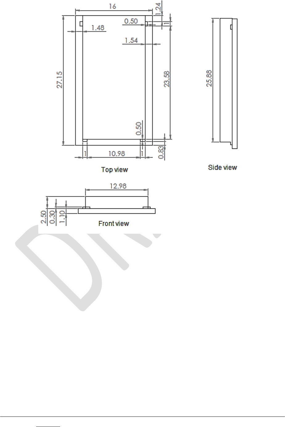
5 Package mechanical data ...................................................................................................... 21
6 Regulatory compliance .......................................................................................................... 22
6.1 CE certification ................................................................................................................. 22
6.2 FCC certification ............................................................................................................... 22
6.3 IC certification................................................................................................................... 22
6.4 Labeling instructions ......................................................................................................... 23
6.5 Product manual instructions ............................................................................................. 24
7 Ordering information .............................................................................................................. 25
Appendix 1 Document revision history ........................................................................................ 26

List of tables
February 2017 DocID0xxxxx Rev 0.xx 3/27
This is preliminary information on a new product now in development or undergoing evaluation. Details are subject to change
without notice. www.st.com
List of tables
Table 1. Recommended operating conditions. ................................................................................ 6
Table 2. Absolute maximum ratings. ............................................................................................... 6
Table 3. I/O operating specifications. .............................................................................................. 6
Table 4. Current consumption. ........................................................................................................ 7
Table 5. RF compliance limits. ........................................................................................................ 7
Table 6 RF sensitivity data. ............................................................................................................ 8
Table 7. Pin assignment. ................................................................................................................ 9
Table 7. Memory resources. ......................................................................................................... 11
Table 8. SPSGPE pins requiring connections, when the module is connected to a host
microcontroller unit. ...................................................................................................................... 12
Table 9. SPSGPE pins requiring connections, when the module is connected to a host computer
via USB. ....................................................................................................................................... 12
Table 10. Outputs to external LED by pin STAT_LED (TP10). ...................................................... 15
Table 11. Soldering profile. ........................................................................................................... 19
Table 12. Ordering information. .................................................................................................... 25
Table 13. Document revision history. ............................................................................................ 26

List of figures
February 2017 DocID0xxxxx Rev 0.xx 4/27
This is preliminary information on a new product now in development or undergoing evaluation. Details are subject to change
without notice. www.st.com
List of figures
Figure 1. Pin Placement (top view of LGA pads placed on bottom side).Errore. Il segnalibro non è definito.
Figure 2. Hardware block diagram ................................................................................................ 11
Figure 3. Typical application circuit of SPSGPE connected to a host microcontroller. ................... 13
Figure 4. Typical application circuit of SPSGPE connected to a host computer via USB. ............. 13
Figure 5. Example of SPSGPE layout. .......................................................................................... 13
Figure 6. Recommended SPSGPE footprint. ................................................................................ 18
Figure 7. Soldering profile. ............................................................................................................ 19
Figure 8. Package mechanical data…………………………………………………………… 21

February 2017 DocID0xxxxx Rev 0.xx 5/27
This is preliminary information on a new product now in development or undergoing evaluation. Details are subject to change
without notice. www.st.com
1 Description
SPSGPE is a hardware LGA-SMT module for easy development of high performance wireless
network applications for a wide range of applications.
Compact-sized, low power and fully integrated, SPSGPE is available in 3 versions:
SPSGPE-433 operating on ETSI 433 MHz band
SPSGPE-868 operating on ETSI 868 MHz band
SPSGPE-915 operating FCC 915 MHz band.
All versions have the same pin-out and mechanical shape.
SPSGPE is based on SPIRIT1 RF sub-GHz transceiver (with integrated SMPS) and
STM32L151RDY6 microcontroller by ST Microelectronics. Balun and filtering network are
embedded in the module. An external antenna can be connected through one pin of the module
which requires an impedance-controlled track of 50 Ω. The UART host interface and USB device
interface allow simple connection to an external microcontroller with a standard firmware or a
host computer, enabling AT commands to facilitate RF configuration, data transmission and
reception, using simple point-to-point communication. Selected STM32L1 GPIO and peripherals
are available to interface external devices and enable user applications. Advanced features of
SPIRIT1 radio are also accessible.
SPSGPE is designed and engineered to build OEM solutions and applications primarily in the
following domains:
Internet of Things (IoT) and Machine-to-Machine (M2M);
Smart Cities;
Smart Grids and Energy Management;
Home & Building Automation;
Wireless Sensor Networks;
Data acquisition equipment management;
Industrial condition and asset monitoring.
February 2017 DocID0xxxxx Rev 0.xx 6/27
This is preliminary information on a new product now in development or undergoing evaluation. Details are subject to change
without notice. www.st.com
2 Hardware specifications
Unless otherwise specified, typical data are based on TA = 25 °C, VDD = 3.3 V.
2.1 Recommended operating conditions
Symbol
Parameter
Min.
Typ.
Max.
Unit
TA
Operating ambient temperature range
-40
-
+85
°C
VDD
Operating supply voltage (1)
1.9
3.3
3.6
V
FREQ
RF frequency 1 for SPSGPE-433
433.05
-
434.79
MHz
FREQ
RF frequency 1 in ETSI band for SPSGPE-868
868
-
868.6
MHz
FREQ
RF frequency 2 in ETSI band for SPSGPE-868
869.4
-
869.65
MHz
FREQ
RF frequency 1 in FCC band for SPSGPE-915
902.0
-
928.0
MHz
(1) USB is not functional below VDD=2.0V. Should be USB compliant from I/O voltage standpoint, the
minimum VDD is 3.0 V. For further details, please refer to STM32L151RDY6 datasheet.
Table 1. Recommended operating conditions.
2.2 Absolute maximum ratings
Symbol
Parameter
Min.
Typ.
Max.
Unit
TSTG
Storage temperature range
-40
-
+85
°C
VDD
Operating supply voltage
-0.3
-
3.9
V
VIO
I/O pin voltage
-0.3
-
5.5
V
Table 2. Absolute maximum ratings.
2.3 I/O operating specifications
Symbol
Parameter
Min.
Typ.
Max.
Unit
VIL(1)
I/O input low level voltage
-0.3
-
0.3 VDD
V
VIH(1)
I/O input high level voltage
0.7 VIN
-
VDD+0.3
V
(1) For further details, please refer to STM32L151RDY6 datasheet, I/O port features.
Table 3. I/O operating specificat
February 2017 DocID0xxxxx Rev 0.xx 7/27
This is preliminary information on a new product now in development or undergoing evaluation. Details are subject to change
without notice. www.st.com
2.4 Current consumption
Symbol
Parameter
Test conditions
Typ.
Unit
IDD
Supply current
Operating mode
TX, +11 dBm, freq. 868MHz
27
mA
IDD
Supply current
Operating mode
TX, +10.5 dBm, freq. 915MHz
39
mA
IDD
Supply current
Operating mode
TX, +10 dBm, freq. 433MHz
24
mA
IDD
Supply current
Operating mode
RX, freq. 868MHz
19
mA
IDD
Supply current
Operating mode
RX, freq. 915MHz
28
mA
IDD
Supply current
Operating mode
RX, freq. 433MHz
18
mA
IDD
Supply current
Stand-by (Radio off, STM32L151RDY6 in Stop
mode with RTC)
5
µA
Table 4. Current consumption.
2.5 RF compliance limits
RF compliance limits for CE and FCC certifications, referring to factory loaded firmware. If applying a
custom firmware, please ensure these limits are not exceeded, voiding CE and FCC certifications.
Standards
Parameter
Max.
Unit
FCC Part 15.207 (1)
FCC Part 15.247 (1)
EN 300 220-2 V2.4.1 (2)
EN 301 489-01 V1.9.2 (2)
EN 301 489-03 V1.4.1 (2)
Data rate
50
kbps
Output power
(ETSI 868 MHz and FCC 915 MHz band)
+10.5
dbm
Output power
(ETSI 433 MHz band)
+10
Modulation
GFSK
(1) FCC standards are only applicable to SPSGPE-915 operating in the FCC 915 MHz band
(2) EN standards are only applicable to SPSGPE-433 and SPSGPE-868 operating in the ETSI
433MHz and ETSI 868MHz respectively.
Table 5. RF compliance limits.

February 2017 DocID0xxxxx Rev 0.xx 8/27
This is preliminary information on a new product now in development or undergoing evaluation. Details are subject to change
without notice. www.st.com
2.6 RF sensitivity data
RF sensitivity data for all the versions of SPSGPE are reported in Table 6.
Parameter
SPSGPE
version
Test conditions
Typ.
Unit
Sensitivity
(1% BER)
SPSGPE-433
FREQ = 434 MHz,
Data Rate = 50 kbps (25 kHz dev.
CH Filter=125kHz),
VDD = 3.3 V, TA = 25°C
Spirit1 SMPS enabled
-98
dBm
Sensitivity
(1% BER)
SPSGPE-868
FREQ = 868 MHz,
Data Rate = 50 kbps (25 kHz dev.
CH Filter=125kHz),
VDD = 3.3 V, TA = 25°C
Spirit1 SMPS enabled
-104
dBm
Sensitivity
(1% BER)
SPSGPE-915
FREQ = 915 MHz,
Data Rate = 50 kbps (25 kHz dev.
CH Filter=125kHz),
VDD = 3.3 V, TA = 25°C
Spirit1 SMPS enabled
-105
dBm
Table 6 RF sensitivity data.

February 2017 DocID0xxxxx Rev 0.xx 9/27
This is preliminary information on a new product now in development or undergoing evaluation. Details are subject to change
without notice. www.st.com
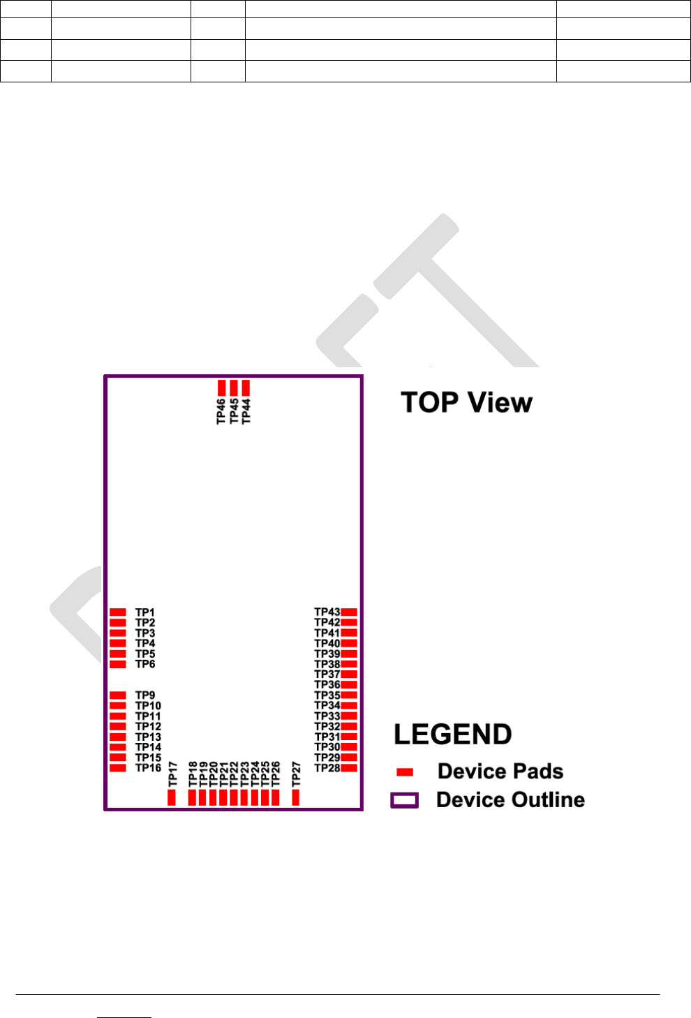
2.7 Pin assignment
Pin
Name
Type
Description
STM32L151RDY6
pin(1)
TP1
I2C1_SCL(4)
I/O
I2C clock(3) or general purpose input/output
PB8
TP2
SWDIO
I/O
Serial wire I/O(2)
PA13
TP3
GPIO_11
I/O
General purpose input/output
PB7
TP4
GPIO_12
I/O
General purpose input/output
PC12
TP5
GPIO_13
I/O
General purpose input/output
PA15
TP6
RESET
I
Reset input, active low, internal pull-up
NRST
TP9
I2C1_SDA(4)
I/O
I2C data in/out(3) or general purpose
input/output
PB9
TP10
STAT_LED
O
Status indicator LED
PB6
TP11
USB_DEV_CONN
I
Pull high, if USB is used/connected,
pull low, if USB is not used/connected
PB5
TP12
GPIO_8
I/O
General purpose input/output
PB4
TP13
GPIO_10
I/O
General purpose input/output
PB3
TP14
PWR_MON
O
Power ON monitor, goes high if the module
is powered on, goes low if the module is not
powered
PC11
TP15
GPIO_14
I/O
General purpose input/output
PD2
TP16
SWCLK
I
Serial wire clock(2)
PA14
TP17
GND
Power
Ground
-
TP18
USB_P / RTS
I/O
USB DATA- or Request to send signal from
DTE, depending on firmware configuration
PA12
TP19
USB_N / CTS
I/O
USB DATA+ or Clear to send signal to DTE,
depending on firmware configuration
PA11
TP20
UART2_RX
I
Serial data input from DTE
PA10
TP21
UART2_TX
O
Serial data output to DTE
PA9
TP22
GPIO_9
I/O
General purpose input/output
PC6
TP23
SPI_MISO(4)
I/O
SPI MISO or general purpose input/output
PB14
TP24
SPI_MOSI(4)
I/O
SPI MOSI or general purpose input/output
PB15
TP25
RI
O
Ring indicator to DTE
PB12
TP26
SPI_CLK(4)
I/O
SPI clock or general purpose input/output
PB13
TP27
VDD
Power
Supply input voltage
-
TP28
DTR
I
Data terminal ready from DTE
PB2
TP29
TX_AUX
O
Auxiliary serial data output for debug/test
PB10
TP30
ADC_01
I/O
ADC input or general purpose input/output
PB0
TP31
GPIO_6
I/O
General purpose input/output
PC5
TP32
GPIO_5
I/O
General purpose input/output
PC4
TP33
ON/OFF
I
Input for switching ON or OFF the module
PA0
TP34
UART1_RX
I/O
Serial data input
PA3
TP35
UART1_TX
I/O
Serial data output
PA2
TP36
ALARM/GPIO_1
I/O
Alarm output or general purpose
input/output
PCO
TP37
GPIO_4
I/O
General purpose input/output
PC3
TP38
GPIO_2/RF_TX_MON
O
RF transmitter ON monitor or general
purpose input/output
PC1
TP39
RX_AUX
I
Auxiliary serial data input for debug/test
PB11
TP40
ADC_01
I/O
ADC input or general purpose input/output
PB1
TP41
RESERVED
-
Must be left unconnected (for future uses)
PA8
TP42
GPIO_7
I/O
General purpose input/output
PA1
February 2017 DocID0xxxxx Rev 0.xx 10/27
This is preliminary information on a new product now in development or undergoing evaluation. Details are subject to change
without notice. www.st.com
TP43
GPIO_3
I/O
General purpose input/output
PC2
TP44
GND
Power
Ground
-
TP45
ANT
I/O
Connection pin for external antenna (50 Ω)
-
TP46
GND
Power
Ground
-
Table 7. Pin assignment.
(1) For further details, please refer to STM32L151RDY6 datasheet, Pin descriptions section.
(2) Do not use SWD interface for any reason, unless to intentionally erase module flash memory and install
a different firmware image. Any attempt to use SWD interface will force an immediate flash memory full
erase, leaving SPSGPE in a clean state. Please notice that “FW Copy Protection Level 1” of
STM32L151RDY6 microcontroller is activated.
(3) For I2C operation at 100 kHz an external pull-up resistor of 4.7 kΩ needs to be used. For I2C operation
at 400 kHz an external pull-up resistor of 4.7 kΩ needs to be used.
(4) Pin may be configured either as the function indicated in the pin name, or as general purpose
input/output.
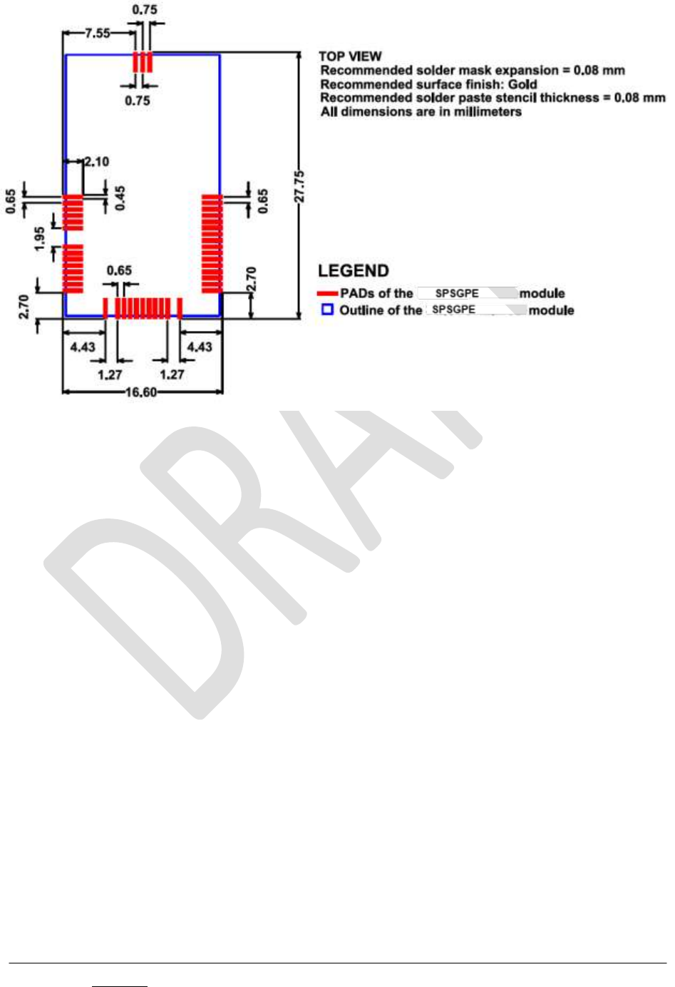
2.8 Pin placement
Figure 1. Pin placement (top view of LGA pads placed on bottom side).
February 2017 DocID0xxxxx Rev 0.xx 11/27
This is preliminary information on a new product now in development or undergoing evaluation. Details are subject to change
without notice. www.st.com
2.9 Memory resources
Memory resources available in the STM32L151RDY6 microcontroller unit adopted in all SPSGPE
versions are listed in Table 8. For further details, please refer to STM32L151RDY6 microcontroller unit
datasheet and user manual, and SPSGPE user manual.
Item
Value
Flash Memory(1)
384 kByte
RAM
48 kByte
I/O(2)
39 channels
Table 8. Memory resources.
(1) Amount of Flash memory available without any firmware installed on SPSGPE. To calculate the
amount of available Flash memory with SPSGPE firmware, please refer to SPSGPE software user
manual. For further details, please refer to STM32L151RDY6 datasheet.
(2) The number of available I/O channels may change depending on actual hardware configuration. For
further details, please refer to par. 0and 0.
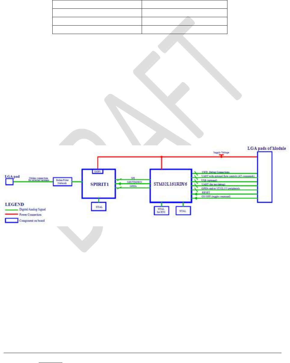
2.10 Hardware block diagram
Figure 1. Hardware block diagram
February 2017 DocID0xxxxx Rev 0.xx 12/27
This is preliminary information on a new product now in development or undergoing evaluation. Details are subject to change
without notice. www.st.com
3 Hardware design
3.1 Pin usage
If used with default firmware and interfaced to a host microcontroller unit, SPSGPE requires minimum
power, ground and UART to transmit and receive signals, that is to be connected. Other signals are
optional and provide additional functionality. Unused signals must be left unconnected.
In case the module is connected to a host microcontroller unit, SPSGPE pins requiring connections are
outlined in Table 9.
Pin
Name
Description
Optional
TP27
VDD
Supply input voltage
No
TP17
GND
Ground
No
TP44
TP46
TP21
UART2_TX
Serial data output to DTE
No
TP20
UART2_RX
Serial data input from DTE
No
TP18
USB_P /
RTS
Request to send signal from DTE, if used.
If flow controls are not used, this pin must be connected to
GND.
It could be left floating, if USB is supported by firmware.
Yes
TP33
ON/OFF
Input for switching ON or OFF the module(1)
(toggle command)
Yes
TP6
RESET
Reset input, active low, internal pull-up(1)
No
TP45
ANT
Connection pin for external antenna (50 Ω)
No
(1) Open drain connection is required.
Table 9. SPSGPE pins requiring connections, when the module is connected to a host
microcontroller unit.
In another typical application circuit, SPSGPE is connected to a host computer through a standard USB
connector. In this case, module pins requiring connections are listed in Table 10.
Pin
Name
Description
Optional
TP27
VDD
Supply input voltage
No
TP17
GND
Ground
No
TP44
TP46
TP18
USB_P / RTS
USB Data– (90 Ω differential)
No
TP19
USB_N / CTS
USB Data+ (90 Ω differential)
No
TP11
USB_DEV_CO
NN
Input for detecting the connection to the USB cable.
Pull it high when USB cable is connected.
No
TP33
ON/OFF
Input for switching module ON or OFF
(toggle command)
Yes
TP6
RESET
Reset input, active low, internal pull-up
No
TP45
ANT
Connection pin for external antenna (50 Ω)
No
Table 10. SPSGPE pins requiring connections, when the module is connected to a host computer
via USB.
February 2017 DocID0xxxxx Rev 0.xx 13/27
This is preliminary information on a new product now in development or undergoing evaluation. Details are subject to change
without notice. www.st.com
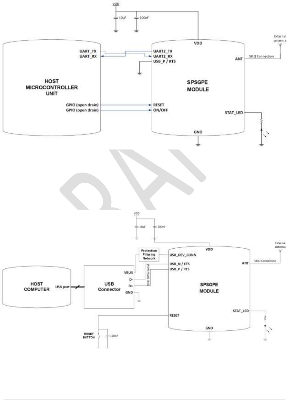
3.2 Typical application circuits
In a typical application circuit, SPSGPE is connected to a host microcontroller unit through a standard
UART to transmit and receive signals. This application is pictured in Figure 2.
Figure 2. Typical application circuit of SPSGPE connected to a host microcontroller.
Please notice that “USB / RTS” could be left floating if USB is supported by firmware.
In another typical application circuit, SPSGPE is connected to a host computer through a standard USB
connector. This application is pictured in Figure 3.
Figure 3. Typical application circuit of SPSGPE connected to a host computer via USB.

February 2017 DocID0xxxxx Rev 0.xx 14/27
This is preliminary information on a new product now in development or undergoing evaluation. Details are subject to change
without notice. www.st.com
NOTE: when using the SPSGPE in a USB self-powered application, USB back-voltage test requirement
must be met (i.e. a maximum of 400 mV may be measured on the VBUS, D+, or D- when the device is not
plugged into a USB port). For this purposes, SPSGPE requires to receive on the pin USB_DEV_CONN a
signal indicating, when set at high logical level, that the VBUS is detected in order to properly control the
internal pull-up resistor connected to D+ line available internally to the STM32L151RDY6. For further
details, please refer to STM32L151RDY6 datasheet.

February 2017 DocID0xxxxx Rev 0.xx 15/27
This is preliminary information on a new product now in development or undergoing evaluation. Details are subject to change
without notice. www.st.com
Special features are enabled by the following pins:
- STAT_LED (pin TP10): output to drive an external LED and indicated status of SPSGPE
connections. If this pin is used as output to an external LED, possible outputs are listed in
Table 11.
LED Output
Description
Periodic single flashing with long
ON time and short OFF time.
Application is waiting for commands from DTE.
Periodic single flashing with short
ON time and long OFF time.
Application has started and SPSGPE is seeking for
connection.
Periodic fast double flashing.
Application has started and SPSGPE is connected to
a gateway.
Table 11. Outputs to external LED by pin STAT_LED (TP10).
- RESET (pin TP6): internal pulled-up signal for resetting SPSGPE. It has to be tied low for at
least 100 ms and then released to perform SPSGPE unconditional hardware restart. Please
notice that unconditional hardware restart must not be used during normal device operation,
since it does not detach the device from the network. It shall be kept as emergency exit
procedure in the rare case the module gets stacked waiting for network response. It is
suggested to implement unconditional hardware restart (through a GPIO of the host
microcontroller unit, to be configured as open drain or through a push button) on SPSGPE
applications only as emergency exit procedure.
- ON/OFF (pin TP33): it performs the turning on/off procedure for SPSGPE when voltage
supply at VDD (pin 27) stands within recommended operating range (please refer to Table 1).
To start the turning off procedure when the module is turned on, the ON/OFF signal needs to
be tied low for at least 2 seconds. Similarly, to start the turning on procedure when the module
is turned off, the ON/OFF signal needs to be tied low for at least 2 seconds. The turning on/off
procedure can also be performed via AT commands (please refer to SPSGPE software
guide).
- PWR_MON (pin TP14): output signal indicating SPSGPE power status. It climbs high when
SPSGPE is properly powered on, and it climbs down when SPSGPE is not powered.
- USB_DEV_CONN (pin TP11): input signal to detect USB cable connections. It has to be high
when USB is connected, and low when USB is disconnected. Considering a 5 V tolerant pin, it
is recommended to connect it to the VBUS pin of USB connector with proper protection and
filtering network, adopting components like diode, ferrite bead and capacitors. If USB is used,
UART interface to DTE is automatically disabled. To re-enable UART, this pin has to be tied
low.

February 2017 DocID0xxxxx Rev 0.xx 16/27
This is preliminary information on a new product now in development or undergoing evaluation. Details are subject to change
without notice. www.st.com
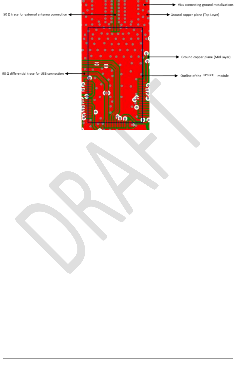
3.3 Layout guidelines
When adopting SPSGPE, please consider the following guidelines for a correct PCB design:
1. A minimum four-layer PCB is suggested.
2. At least one of the PCB layers should be used to implement a copper ground plane
without cuts.
3. Copper planes and/or heavy traces are recommended to implement power supply
connections.
4. Decoupling capacitors (recommended values are 100 nF and 10 µF in parallel) have to
be placed very close to power supply pins.
5. Routing of traces (especially noisy and high frequency ones) across the power supply
should be avoided.
6. The ANT pin (pin TP45) needs to be used for connecting the module to an external
antenna. Its related RF ground is represented by pins TP44 and TP46. A trace having a
controlled impedance of 50 Ω needs to be used to connect the ANT pin (pin TP45) to an
external antenna (microstrip or grounded coplanar waveguide solutions of 50 Ω are
suggested).
7. Routing of traces (especially noisy, high frequency and power supply ones) near or
across the connection between the ANT pin (pin TP45) and the external antenna should
be avoided.
8. Connection of all ground metallization and/or layers should have as many vias as
possible. Number and density of these vias should be increased in the connection area
between the ANT pin (pin TP45) and the external antenna.
9. A differential trace of 90 Ω needs to be used to connect pins TP18 and TP19 (USB_P /
RTS and USB_N / CTS, respectively) to a USB connector, in case they are used as USB
traces. It is also strongly recommended to follow all hardware and layout guidelines by
USB standards.
An example of SPSGPE layout is pictured in
Figure 4.
February 2017 DocID0xxxxx Rev 0.xx 19/27
This is preliminary information on a new product now in development or undergoing evaluation. Details are subject to change
without notice. www.st.com
3.5 Module reflow installation
SPSGPE is a surface mount module supplied on a 46-pin, 6-layer PCB, with gold surface finish. Final
assembly recommended reflow profile is outlined below, based on IPC/JEDEC JSTD-020C, July 2004
recommendations.
Profile feature
Lead-free assembly
Average ramp-up rate (TSMAX to TP)
1.7°C/sec max
Preheat:
- Temperature min (TS min.)
- Temperature max (TS max.)
- Time (TS min. to TS max.) (tS)
150°C
200°C
60-100 sec (suggested: 85 sec)
Time maintained above:
- Temperature TL
- Temperature TL
217 °C
60-100 sec (suggested: 99 sec)
Peak temperature (TP)
242 °C
Time within 5°C of actual peak temperature (TP)
10-20 sec
Ramp-down rate
2°C/sec
Time from 25°C to peak temperature
8 minutes max.
Table 12. Soldering profile.
Figure 6. Soldering profile.

February 2017 DocID0xxxxx Rev 0.xx 20/27
This is preliminary information on a new product now in development or undergoing evaluation. Details are subject to change
without notice. www.st.com
4 Module operation
SPSGPE software architecture is based on SPSGPE.OS operating system and provides a set of
precompiled firmware libraries to manage module operation.
Two operational modes are supported:
SPSGPE working as a “communication module”, using AT/HDLC commands;
SPSGPE working as a “standalone module”, running embedded standalone application.
When using SPSGPE as a communication module, the module acts as a wireless RF module.
SPSGPE.OS operating system handles SPSGPE internal transceiver and any external device connected
to it, providing mesh routing connectivity. Thus, it allows to configure SPSGPE either as a node or as a
gateway, enabling different application domains including and not limited to low-power applications.
This operational mode enables module configuration and status interrogation, and supports two different
high-level communication interfaces: AT command set and HDLC command interface.
AT and HDLC command interfaces assume communications with an external host processor via USB
and/or UART serial interfaces, in a scenario where SPSGPE acts as an RF modem device and the user
application runs on the host processor.
The two types of command modes are briefly described below:
- AT command: it implements a set of AT commands compliant with Hayes standard AT
command set and expanded through Paradox Engineering proprietary AT command set for
special purposes.
- HDLC command: it offers a fast optimized binary HDLC protocol with a set of HDLC
commands for managing and controlling SPSGPE.
When using SPSGPE as a standalone module, the user can develop its own application code and link it
to SPSGPE.OS, or customize a standard SPSGPE application firmware image through the scripting tool.
Once developed with the scripting tool, compiled script programs can be uploaded and executed under the
control of SPSGPE Script Engine.
For further details about SPSGPE software architecture, command and operating modes, please refer to
SPSGPE Application and Software – User Guide (document reference: tbd)

February 2017 DocID0xxxxx Rev 0.xx 22/27
This is preliminary information on a new product now in development or undergoing evaluation. Details are subject to change
without notice. www.st.com
6 Regulatory compliance
NOTE: this section will be completed and confirmed after the certification process is done.
6.1 CE certification
SPSGPE-433 and SPSGPE-868 are certified in accordance with the following standards:
EN 300 220-2 V2.4.1
EN 301 489-01 V1.9.2
EN 301 489-03 V1.6.1
Receiver category: Class 2 receiver.
6.2 FCC certification
SPSGPE-915 is certified in accordance with the following standards:
FCC Part 15.207
FCC Part 15.247
FCC ID: S9NSPSGPE
6.3 IC certification
SPSGPE-915 is certified in accordance with the following standards:
RSS-247 Issue 1
IC ID: 8976C-SPSGPE
(Please, refer to Appendix A of this document for the French translation).

February 2017 DocID0xxxxx Rev 0.xx 23/27
This is preliminary information on a new product now in development or undergoing evaluation. Details are subject to change
without notice. www.st.com
6.4 Labeling instructions
When integrating SPSGPE-915 into a finished product, the OEM must ensure that FCC labeling
requirements are satisfied. A statement must be placed over the finished product to indicate it includes a
certified module. The label should state the following (or similar wording that conveys the same meaning):
Contains FCC ID: S9NSPSGPE
OR
This product contains FCC ID: S9NSPSGPE
The OEM must place the following statements over the finished product unless it is too small (e.g. less
than 4 x 4 inches):
This device complies with Part 15 of FCC Rules. Operation is subject to the following
two conditions: (1) this device may not cause harmful interference, and (2) this device
must accept any interference received, including any interference that may cause
undesired operation.
When integrating SPSGPE-915 into a finished product, the OEM must ensure that IC labeling
requirements are satisfied. A statement must be placed over the finished product to indicate it includes a
certified module. The label should state the following (or similar wording that conveys the same meaning):
Contains IC ID: 8976C-SPSGPE
OR
This product contains IC ID: 8976C-SPSGPE
The OEM must place the following statements over the finished product unless it is too small (e.g. less
than 4 x 4 inches):
This device complies with RSS-247 of IC Rules. Operation is subject to the following
two conditions: (1) this device may not cause harmful interference, and (2) this device
must accept any interference received, including any interference that may cause
undesired operation.

February 2017 DocID0xxxxx Rev 0.xx 24/27
This is preliminary information on a new product now in development or undergoing evaluation. Details are subject to change
without notice. www.st.com
6.5 Product manual instructions
This paragraph applies to OEM finished products containing SPSGPE and subject to FCC compliance.
The finished product manual must contain the following statement (or similar wording that conveys the
same meaning):
WARNING: Changes or modifications not expressly approved by the party responsible
for compliance could void the user’s authority to operate the equipment.
In cases the OEM seeks Class B (residential) limits for the finished product, the following statement must
be included in the finished product manual:
NOTE: This equipment has been tested and found to comply with the limits for a
Class B digital device, pursuant to Part 15 of FCC Rules. These limits are designed to
provide reasonable protection against harmful interference in a residential installation.
This equipment generates, uses and can radiate radio frequency energy and, if not
installed and used in accordance with given instructions, may cause harmful
interference to radio communications. However, there is no guarantee that interference
will not occur under certain circumstances. If this equipment does cause harmful
interference to radio or television reception, which can be determined by turning the
equipment off and on, the user is encouraged to try to correct the interference by one
or more of the following measures:
– Reorient or relocate the receiving antenna.
– Increase the separation between the equipment and receiver.
– Connect the equipment into an outlet on a circuit different from that to which the
receiver is connected.
– Consult the dealer or an experienced radio/TV technician for help.
In cases the OEM seeks Class A digital device category for the finished product, the following statement
must be included in the finished product manual:
NOTE: This equipment has been tested and found to comply with the limits for a
Class A digital device, pursuant to Part 15 of FCC Rules. These limits are designed to
provide reasonable protection against harmful interference when the equipment is
operated in a commercial environment. This equipment generates, uses, and can
radiate radio frequency energy and, if not installed and used in accordance with the
instruction manual, may cause harmful interference to radio communications.
Operation of this equipment in a residential area is likely to cause harmful interference
in which case the user will be required to correct the interference at his own expenses.

February 2017 DocID0xxxxx Rev 0.xx 25/27
This is preliminary information on a new product now in development or undergoing evaluation. Details are subject to change
without notice. www.st.com
7 Ordering information
Product name
EAN code
Description
SPSGPE-433
tbd
Version operating on ETSI 433 MHz band (Region 1,
Europe)
SPSGPE-868
tbd
Version operating on ETSI 868 MHz band (Region 1,
Europe
SPSGPE-915
tbd
Version operating on FCC 915 MHz band (Region 2,
The Americas)
Table 13. Ordering information.

February 2017 DocID0xxxxx Rev 0.xx 26/27
This is preliminary information on a new product now in development or undergoing evaluation. Details are subject to change
without notice. www.st.com
Appendix A
Déclaration de conformité
A.1 Certification FCC
Le module SPSGPE-915 a été testé et déclaré conforme avec la section 15 de la Règlementation
FCC. Ces limitations sont stipulées afin de procurer une protection raisonnable contre les
interférences gênantes dans les installations approuvées. Cet appareil génère, utilise et diffuse des
ondes radio et, s’il n’est pas installé et utilisé en conformité avec les instructions dont il fait l’objet,
peut causer des interférences gênantes sur les communications radio.
Il n’y a cependant pas de garantie qu’une interférence ne se produira pas dans une installation
particulière.
Cet appareil est en conformité avec la section 15 des règlements FCC. L’utilisation est soumise
aux deux conditions suivantes: (1) cet appareil ne doit pas causer d'interférences nocives, et (2)
Cet appareil doit supporter toute interférence reçue, y compris des interférences qui peuvent
provoquer un fonctionnement non désiré.
Tout changement ou modification fait(e) à cet appareil et non expressément approuvé(e) par
STMicroelectronics peut annuler l’autorisation pour l’utilisateur de faire fonctionner l’appareil.
Approbation du module
FCC ID: S9NSPSGPE
Conformément à la section 15 des règlements FCC, le module SPSGPE-915 est répertorié comme un
dispositif émetteur modulaire.
Ce module n’est évalué que pour une utilisation autonome. Les produits finis incorporant plusieurs
émetteurs doivent être conformes à la colocation et aux exigences d'exposition RF en
concordance avec les procédures FCC multi-émetteurs. D’autres émetteurs fonctionnant dans des
dispositifs portables exposés aux RF (par exemple, situés à moins de 20 cm des personnes avec
dispositifs portatifs ou portés contre le corps) peuvent nécessiter d'une approbation séparée.
A.1.1 Instructions d'étiquetage
Lors de l'intégration du module SPSGPE-915 dans le produit final, le fabricant doit s’assurer que
les exigences en matière d'étiquetage de la FCC sont satisfaites. Une déclaration doit être placée
sur l’étiquette extérieure du produit final indiquant que le produit comprend un module certifié.
L'étiquette doit comporter les informations suivantes (ou une mention analogue que recouvre la
même notion):
Contient FCC ID: S
9NSPSGPE
OU Ce produit contient FCC ID: S9NSPSGPE
Le sous-traitant doit inclure les énoncés suivants sur l’étiquette extérieure du produit final à
moins que le produit ne soit trop petit (par exemple moins de 4 x 4 pouces):
Cet appareil est en conformité avec la section 15 des règlements FCC. L’utilisation est soumise
aux deux conditions suivantes:
(1) cet appareil ne doit pas causer d'interférences nocives, et
(2) Cet appareil doit supporter toute interférence reçue, y compris des interférences qui peuvent provoquer un
fonctionnement non désiré.

February 2017 DocID0xxxxx Rev 0.xx 27/27
This is preliminary information on a new product now in development or undergoing evaluation. Details are subject to change
without notice. www.st.com
A.1.2 Instructions pour l’utilisation du produit
La présente section concerne les produits finis contenant le module SPSGPE-915, assujettis aux
normes FCC. Le manuel du produit final doit contenir la déclaration suivante (ou une mention
analogue que recouvre la même notion):
“ Avertissement: Les changements ou modifications non expressément approuvés par la partie
responsable de la conformité pourraient annuler l'autorisation de l'utilisateur de faire
fonctionner cet équipement. (Section 15.21)”
Dans le cas où le produit finis d’un fabriquant OEM rentre dans les limites de la Classe B
(résidentiel), les énoncés suivants doivent être inclus dans le manuel du produit finis:
“Remarque : Cet équipement a été testé et déclaré conforme aux limitations prévues dans le cadre
de la classe B des appareils numériques, définies par la section 15 du règlement de la FCC. Ces
limites sont conçues pour fournir une protection raisonnable contre toute interférence
dangereuse issue d'une installation résidentielle. Cet équipement produit, utilise et peut émettre
de l'énergie radio électrique et, s'il n'est pas installé et utilisé conformément aux présentes
instructions, peut causer des interférences nuisibles aux communications radio. Cependant, il se
peut que des interférences se produisent dans une installation particulière. Si cet appareil cause
des interférences nuisibles à la réception des signaux de radio ou de télévision, ce qui peut être
déterminé en allumant et en éteignant l'appareil, on encourage l'utilisateur d'essayer de corriger
ces interférences par l'un des moyens suivants:
– Réorienter ou repositionner l'antenne de réception.
– Augmenter la distance séparant l’équipement du récepteur.
– Connecter l’équipement à une prise appartenant à un circuit différent de celui sur
lequel le récepteur est connecté.
– Consulter le revendeur ou un technicien radio/TV expérimenté pour obtenir de l’aide.”
Dans le cas où le produit fini d’un sous-traitant rentre dans les limites imposées aux
appareils numériques de classe A, les énoncés suivants doivent être inclus dans le manuel
du produit finis:
“REMARQUE : Cet appareil a été testé et certifié conforme aux spécifications d'un appareil
électronique de classe A (class A digital device), conformément à la partie 15 du règlement de la
FCC. Ces contraintes sont destinées à fournir une protection raisonnable contre les interférences
nuisibles quand l'appareil est utilisé dans une installation commerciale. Cet équipement produit,
utilise et peut émettre de l'énergie radio électrique et, s'il n'est pas installé et utilisé
conformément aux présentes instructions, peut causer des interférences nuisibles aux
communications radio. L'utilisation de cet appareil dans une installation résidentielle peut
entraîner des interférences nuisibles et l'utilisateur devra corriger les interférences à ses propres
frais.”

February 2017 DocID0xxxxx Rev 0.xx 28/27
This is preliminary information on a new product now in development or undergoing evaluation. Details are subject to change
without notice. www.st.com
A.2 Certification IC (a)
Le module SPSGPE-915 a été testé et déclaré conforme avec la Règlementation IC CNR-210. Ces
limitations sont stipulées afin de procurer une protection raisonnable contre les interférences
gênantes en installations approuvées. Cet appareil génère, utilise et diffuse des ondes radio et, s’il
n’est pas installé et utilisé en conformité avec les instructions dont il fait l’objet, peut causer des
interférences gênantes sur les communications radio.
Il n’y a cependant pas de garantie qu’une interférence ne se produira pas dans une installation
particulière.
Ce produit répond aux exigences de la norme CNR-210 d'Industrie Canada. Son fonctionnement
est soumis aux deux conditions suivantes:
(1) cet appareil ne doit pas causer d'interférences nocives, et
(2) Cet appareil doit supporter toute interférence reçue, y compris des interférences qui peuvent
provoquer un fonctionnement non désiré.
Tout changement ou modification fait(e) à cet appareil et non expressément approuvé(e) par
STMicroelectronics peut annuler l’autorisation pour l’utilisateur de faire fonctionner l’appareil.
Approbation du module
IC: 8976C-SPSGPE
Conformément à IC CNR-210, le module SPSGPE-915 est répertorié comme un dispositif émetteur
modulaire
Ce module n’est évalué que pour une utilisation autonome. Les produits finis incorporant plusieurs
émetteurs doivent être conformes à la colocation et aux exigences d'exposition RF en
concordance avec les procédures FCC multi-émetteurs. D’autres émetteurs fonctionnant dans des
dispositifs portables exposés aux RF (par exemple, situés à moins de 20 cm des personnes avec
dispositifs portatifs ou portés contre le corps) peuvent nécessiter d'une approbation séparée.
A.2.1 Instructions d'étiquetage
Lors de l'intégration du module SPSGPE-915 dans le produit final, le fabricant doit s’assurer que
les exigences en matière d'étiquetage de la IC sont satisfaites. Une déclaration doit être placée
sur l’étiquette extérieure du produit final indiquant que le produit comprend un module certifié.
L'étiquette doit comporter les informations suivantes (ou une mention analogue que recouvre la
même notion):
Contient IC ID: 8976C-SPSGPE
OU Ce produit contient IC ID: 8976C-SPSGPE
Le sous-traitant doit inclure les énoncés suivants sur l’étiquette extérieure du produit final à
moins que le produit ne soit trop petit (par exemple moins de 4 x 4 pouces):
Cet appareil est en conformité aux normes IC. L’utilisation est soumise aux deux conditions
suivantes:
(1) cet appareil ne doit pas causer d'interférences nocives, et
(2) Cet appareil doit supporter toute interférence reçue, y compris des interférences qui peuvent
provoquer un fonctionnement non désiré

February 2017 DocID0xxxxx Rev 0.xx 29/27
This is preliminary information on a new product now in development or undergoing evaluation. Details are subject to change
without notice. www.st.com
A.2.2 Instructions pour l’utilisation du produit
La présente section concerne les produits finis contenant le module SPSGPE-915, assujettis aux
normes IC. Le manuel du produit final doit contenir la déclaration suivante (ou une mention
analogue que recouvre la même notion):
“Avertissement: Les changements ou modifications non expressément approuvés par la partie
responsable de la conformité pourraient annuler l'autorisation de l'utilisateur de faire
fonctionner cet équipement. (CNR-210)”
Dans le cas où le produit finis d’un fabriquant OEM rentre dans les limites de la Classe B
(résidentiel), les énoncés suivants doivent être inclus dans le manuel du produit finis:
“ Remarque : Cet équipement a été testé et déclaré conforme aux limitations prévues dans le cadre
de la classe B des appareils numériques, définies par la norme CNR-210 d'Industrie Canada.
Ces limites sont conçues pour fournir une protection raisonnable contre toute interférence
dangereuse issue d'une installation résidentielle. Cet équipement produit, utilise et peut émettre
de l'énergie radio électrique et, s'il n'est pas installé et utilisé conformément aux présentes
instructions, peut causer des interférences nuisibles aux communications radio. Cependant, il se
peut que des interférences se produisent dans une installation particulière. Si cet appareil cause
des interférences nuisibles à la réception des signaux de radio ou de télévision, ce qui peut être
déterminé en allumant et en éteignant l'appareil, nous encourageons l'utilisateur à essayer de
corriger ces interférences par l'un des moyens suivants:
– Réorienter ou repositionner l'antenne de réception.
– Augmenter la distance séparant l’équipement du récepteur.
– Connecter l’équipement à une prise appartenant à un circuit différent de celui sur
lequel le récepteur est connecté.
– Consulter le revendeur ou un technicien radio/TV expérimenté pour obtenir de l’aide.”
Dans le cas où le produit finis d’un fabriquant OEM rentre dans le cadre des limites imposées aux
appareils numériques de classe A, les énoncés suivants doivent être inclus dans le manuel du
produit finis:
“ REMARQUE: Cet appareil a été testé et certifié conforme aux spécifications d'un appareil
électronique de classe A (class A digital device), conformément à la norme CNR-210 d'Industrie
Canada. Ces contraintes sont destinées à fournir une protection raisonnable contre les
interférences nuisibles quand l'appareil est utilisé dans une installation commerciale. Cet
équipement produit, utilise et peut émettre de l'énergie radio électrique et, s'il n'est pas installé et
utilisé conformément aux présentes instructions, peut causer des interférences nuisibles aux
communications radio. L'utilisation de cet appareil dans une installation résidentielle peut entraîner
des interférences nuisibles et l'utilisateur devra corriger les interférences à ses propres frais.”

February 2017 DocID0xxxxx Rev 0.xx 30/27
This is preliminary information on a new product now in development or undergoing evaluation. Details are subject to change
without notice. www.st.com
A.3 Certification CE
Le module SPSGPE a obtenu une certification de conformité aux normes suivantes:
– EN 300 328 V1.8.1 :2012
– EN 300 328 V1.9.1 :2015
– EN 301 489-17 V2.2.1 :2009
– EN 301 489-1 V1.9.2:2011
– EN 62479 :2010
– EN60950-1:2006 + A11:2009 + A1:2010 + A12:2011 + A2 :2013
Le module est certifié CE.


February 2017 DocID0xxxxx Rev 0.xx 32/27
This is preliminary information on a new product now in development or undergoing evaluation. Details are subject to change
without notice. www.st.com
Appendix 1 Document revision history
Date
Revision
Changes
2016-09-15
1.0
First release
2016-10-11
1.1
by A.R.
2017-02-16
1.2
By A.R.
Table 14. Document revision history

February 2017 DocID0xxxxx Rev 0.xx 33/27
This is preliminary information on a new product now in development or undergoing evaluation. Details are subject to change
without notice. www.st.com
Please Read Carefully:
Information in this document is provided solely in connection with ST products. STMicroelectronics NV and its subsidiaries (“ST”) reserve the right
to make changes, corrections, modifications or improvements, to this document, and the products and services described herein at any time,
without notice.
All ST products are sold pursuant to ST’s terms and conditions of sale.
Purchasers are solely responsible for the choice, selection and use of the ST products and services described herein, and ST assumes no liability
whatsoever relating to the choice, selection or use of the ST products and services described herein.
No license, express or implied, by estoppel or otherwise, to any intellectual property rights is granted under this document. If any part of this
document refers to any third party products or services it shall not be deemed a license grant by ST for the use of such third party products or
services, or any intellectual property contained therein or considered as a warranty covering the use in any manner whatsoever of such third
party products or services or any intellectual property contained therein.
UNLESS OTHERWISE SET FORTH IN ST’S TERMS AND CONDITIONS OF SALE ST DISCLAIMS ANY EXPRESS OR IMPLIED WARRANTY WITH RESPECT
TO THE USE AND/OR SALE OF ST PRODUCTS INCLUDING WITHOUT LIMITATION IMPLIED WARRANTIES OF MERCHANTABILITY, FITNESS FOR A
PARTICULAR PURPOSE (AND THEIR EQUIVALENTS UNDER THE LAWS OF ANY JURISDICTION), OR INFRINGEMENT OF ANY PATENT, COPYRIGHT
OR OTHER INTELLECTUAL PROPERTY RIGHT.
ST PRODUCTS ARE NOT DESIGNED OR AUTHORIZED FOR USE IN: (A) SAFETY CRITICAL APPLICATIONS SUCH AS LIFE SUPPORTING, ACTIVE
IMPLANTED DEVICES OR SYSTEMS WITH PRODUCT FUNCTIONAL SAFETY REQUIREMENTS; (B) AERONAUTIC APPLICATIONS; (C) AUTOMOTIVE
APPLICATIONS OR ENVIRONMENTS, AND/OR (D) AEROSPACE APPLICATIONS OR ENVIRONMENTS. WHERE ST PRODUCTS ARE NOT DESIGNED
FOR SUCH USE, THE PURCHASER SHALL USE PRODUCTS AT PURCHASER’S SOLE RISK, EVEN IF ST HAS BEEN INFORMED IN WRITING OF SUCH
USAGE, UNLESS A PRODUCT IS EXPRESSLY DESIGNATED BY ST AS BEING INTENDED FOR “AUTOMOTIVE, AUTOMOTIVE SAFETY OR MEDICAL”
INDUSTRY DOMAINS ACCORDING TO ST PRODUCT DESIGN SPECIFICATIONS. PRODUCTS FORMALLY ESCC, QML OR JAN QUALIFIED ARE
DEEMED SUITABLE FOR USE IN AEROSPACE BY THE CORRESPONDING GOVERNMENTAL AGENCY.
Resale of ST products with provisions different from the statements and/or technical features set forth in this document shall immediately void
any warranty granted by ST for the ST product or service described herein and shall not create or extend in any manner whatsoever, any liability
of ST.
ST and the ST logo are trademarks or registered trademarks of ST in various countries.
Information in this document supersedes and replaces all information previously supplied.
The ST logo is a registered trademark of STMicroelectronics. All other names are the property of their respective owners.
© 2014 STMicroelectronics - All rights reserved
STMicroelectronics group of companies
Australia - Belgium - Brazil - Canada - China - Czech Republic - Finland - France - Germany - Hong Kong - India - Israel - Italy - Japan -
Malaysia - Malta - Morocco - Philippines - Singapore - Spain - Sweden - Switzerland - United Kingdom - United States of America
www.st.com