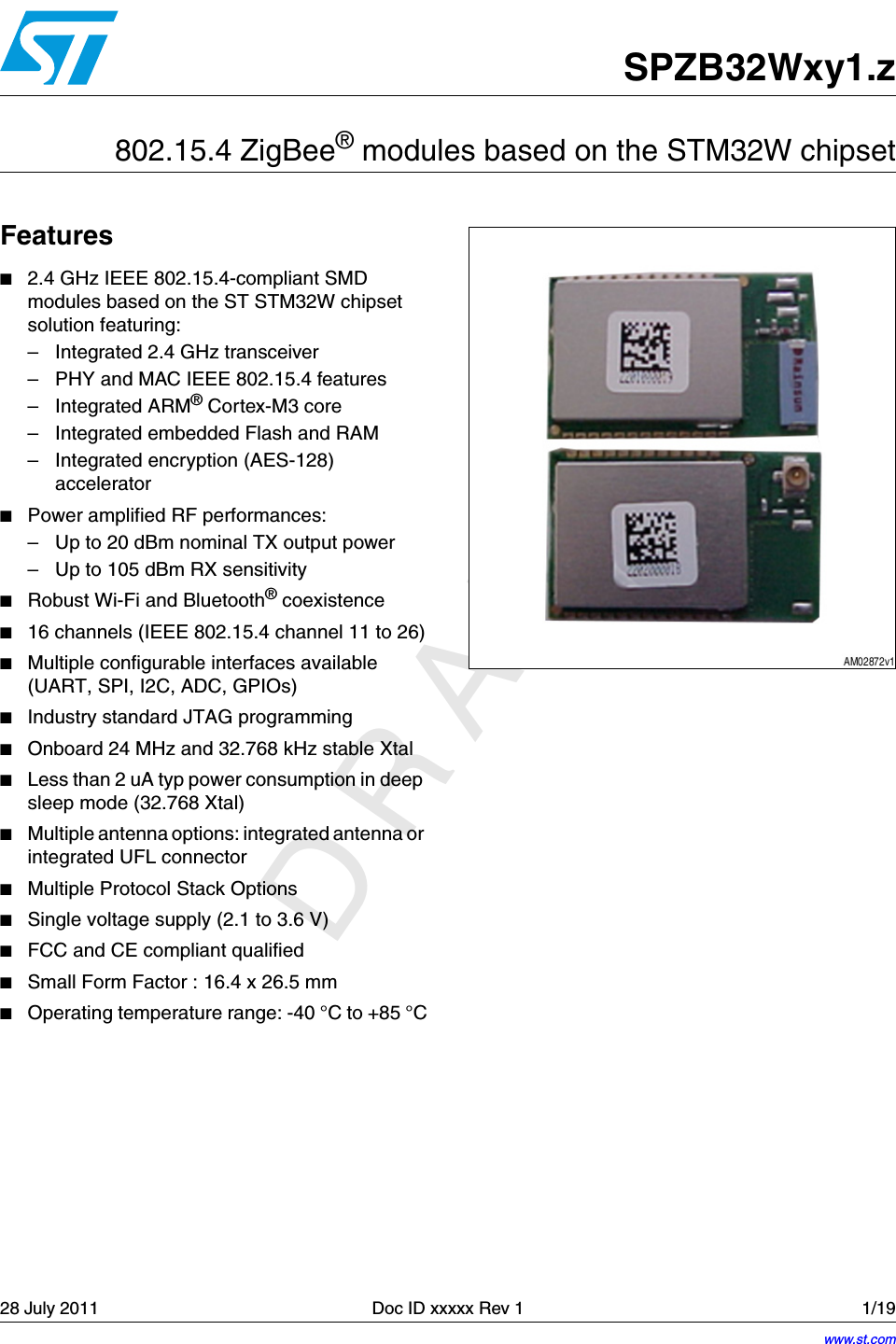
ST Microelectronics S R L ZB32C1 SPZB32Wxy1.z series IEE802.15.4 / ZigBee® Module User Manual SPZB32Wxy1 z
ST Microelectronics S.R.L. SPZB32Wxy1.z series IEE802.15.4 / ZigBee® Module SPZB32Wxy1 z
Contents
- 1. Manual
- 2. Modular label instructions
Manual
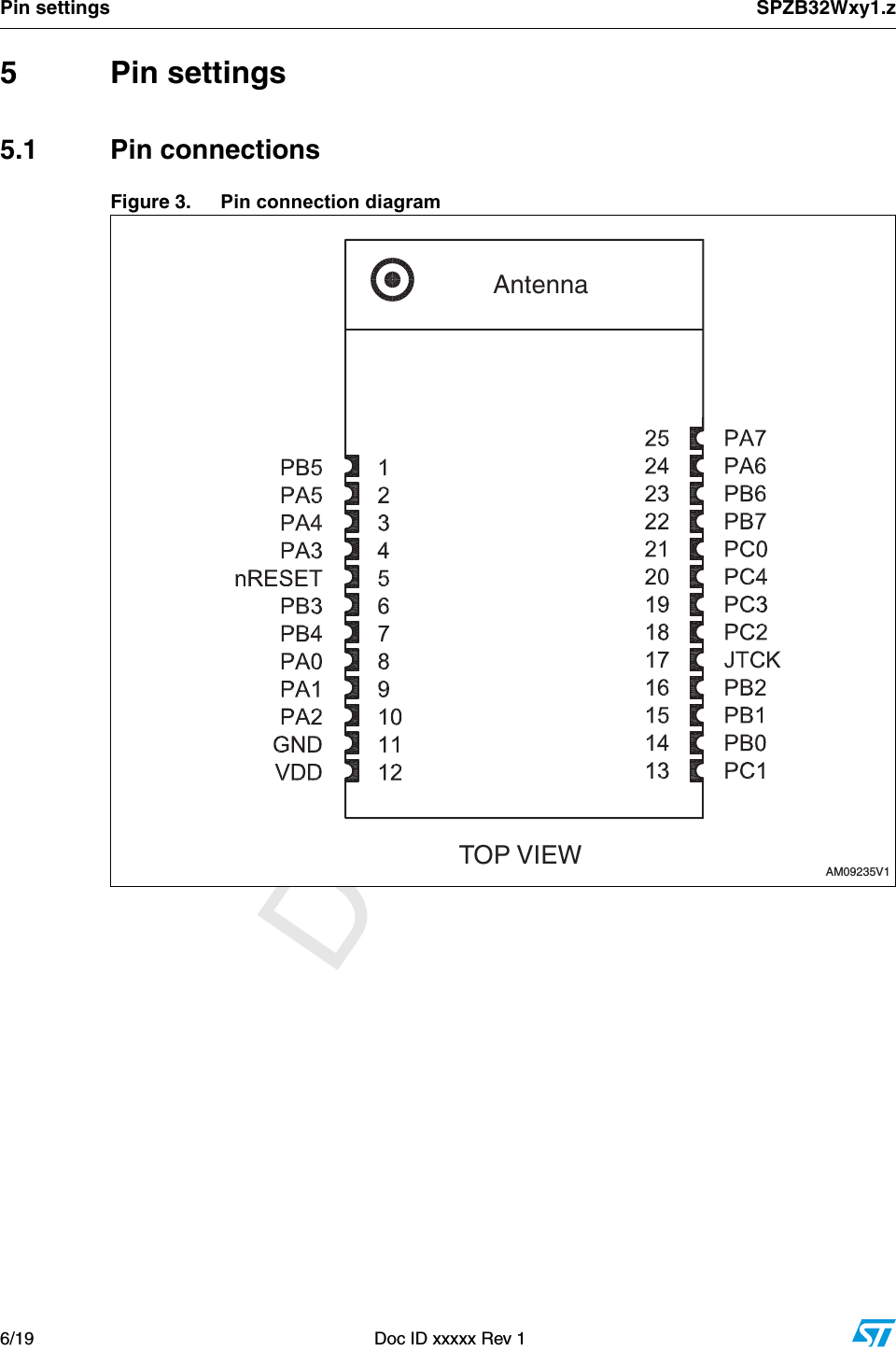
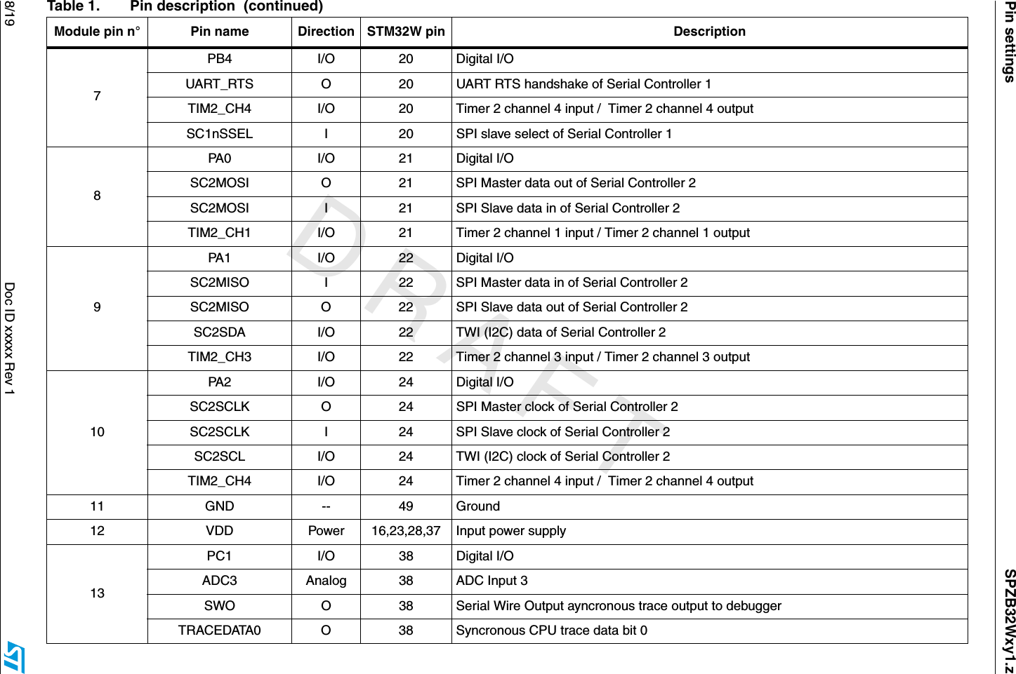
![DRAFTSPZB32Wxy1.z Pin settingsDoc ID xxxxx Rev 1 7/195.2 Pin description Table 1. Pin description Module pin n° Pin name Direction STM32W pin Description1PB5 I/O 43 Digital I/OADC0 Analog 43 ADC Input 0TIM2CLK I 43 Timer 2 external clock inputTIM1MSK I 43 Timer 1 external clock mask input2PA5 I/O 27 Digital I/OADC5 Analog 27 ADC Input 1PTI_DATA O 27 Frame signal of PTI (Packet Trace Interface) nBOOTMODE I 27 Embedded serial bootloader activation out of resetTRACEDATA3 0 27 Synchrounus CPU trace data bit 33PA4 I/O 26 Digital I/OADC4 Analog 26 ADC Input 0PTI_EN O 26 Frame signal of PTI (Packet Trace Interface) TRACEDATA2 O 26 Synchrounus CPU trace data bit 24PA3 I/O 25 Digital I/OSC2nSSEL I 25 SPI SLAVE SELECT of Serial Controller 2TIM2_CH2 I/O 25 Timer 2 channel 2 output (or input - Disable remap with TIM2_OR[5])TRACECLK O 25 Synchrounus CPU trace clock5 nRESET I 12 Active low reset ( an internal pull-up of 30 kohm typ. is provided)6PB3 I/O 19 Digital I/OUART_CTS I 19 UART CTS handshake of Serial Controller 1SC1SCLK I/O 19 SPI slaver clock of Serial Controller SC1 / SPI master clock of Serial Controller SC1TIM2_CH3 I/O 19 Timer 2 channel 3 input / Timer 2 channel 3 output](https://usermanual.wiki/ST-Microelectronics-S-R-L/ZB32C1.Manual/User-Guide-1573694-Page-7.png)