ST Microelectronics S R L ZB32C1 SPZB32Wxy1.z series IEE802.15.4 / ZigBee® Module User Manual SPZB32Wxy1 z
ST Microelectronics S.R.L. SPZB32Wxy1.z series IEE802.15.4 / ZigBee® Module SPZB32Wxy1 z
Contents
- 1. Manual
- 2. Modular label instructions
Manual
DRAFT
28 July 2011 Doc ID xxxxx Rev 1 1/19
19
SPZB32Wxy1.z
802.15.4 ZigBee® modules based on the STM32W chipset
Features
■2.4 GHz IEEE 802.15.4-compliant SMD
modules based on the ST STM32W chipset
solution featuring:
– Integrated 2.4 GHz transceiver
– PHY and MAC IEEE 802.15.4 features
– Integrated ARM® Cortex-M3 core
– Integrated embedded Flash and RAM
– Integrated encryption (AES-128)
accelerator
■Power amplified RF performances:
– Up to 20 dBm nominal TX output power
– Up to 105 dBm RX sensitivity
■Robust Wi-Fi and Bluetooth® coexistence
■16 channels (IEEE 802.15.4 channel 11 to 26)
■Multiple configurable interfaces available
(UART, SPI, I2C, ADC, GPIOs)
■Industry standard JTAG programming
■Onboard 24 MHz and 32.768 kHz stable Xtal
■Less than 2 uA typ power consumption in deep
sleep mode (32.768 Xtal)
■Multiple antenna options: integrated antenna or
integrated UFL connector
■Multiple Protocol Stack Options
■Single voltage supply (2.1 to 3.6 V)
■FCC and CE compliant qualified
■Small Form Factor : 16.4 x 26.5 mm
■Operating temperature range: -40 °C to +85 °C
www.st.com

DRAFT
Contents SPZB32Wxy1.z
2/19 Doc ID xxxxx Rev 1
Contents
1 Description . . . . . . . . . . . . . . . . . . . . . . . . . . . . . . . . . . . . . . . . . . . . . . . . . 3
2 RoHS compliance . . . . . . . . . . . . . . . . . . . . . . . . . . . . . . . . . . . . . . . . . . . 4
3 Application . . . . . . . . . . . . . . . . . . . . . . . . . . . . . . . . . . . . . . . . . . . . . . . . . 4
4 Block diagram . . . . . . . . . . . . . . . . . . . . . . . . . . . . . . . . . . . . . . . . . . . . . . 5
5 Pin settings . . . . . . . . . . . . . . . . . . . . . . . . . . . . . . . . . . . . . . . . . . . . . . . . 6
5.1 Pin connections . . . . . . . . . . . . . . . . . . . . . . . . . . . . . . . . . . . . . . . . . . . . . 6
5.2 Pin description . . . . . . . . . . . . . . . . . . . . . . . . . . . . . . . . . . . . . . . . . . . . . . 7
6 Electrical characteristics . . . . . . . . . . . . . . . . . . . . . . . . . . . . . . . . . . . . 11
6.1 Absolute maximum ratings . . . . . . . . . . . . . . . . . . . . . . . . . . . . . . . . . . . . 11
6.2 Recommended operating conditions . . . . . . . . . . . . . . . . . . . . . . . . . . . . 11
6.3 DC electrical characteristics . . . . . . . . . . . . . . . . . . . . . . . . . . . . . . . . . . . 11
6.4 Digital I/O specifications . . . . . . . . . . . . . . . . . . . . . . . . . . . . . . . . . . . . . . 12
6.5 RF electrical characteristics . . . . . . . . . . . . . . . . . . . . . . . . . . . . . . . . . . . 12
7 Mechanical dimensions . . . . . . . . . . . . . . . . . . . . . . . . . . . . . . . . . . . . . 13
8 Soldering . . . . . . . . . . . . . . . . . . . . . . . . . . . . . . . . . . . . . . . . . . . . . . . . . 14
9 Product approvals . . . . . . . . . . . . . . . . . . . . . . . . . . . . . . . . . . . . . . . . . . 15
9.1 FCC approvals . . . . . . . . . . . . . . . . . . . . . . . . . . . . . . . . . . . . . . . . . . . . . 15
9.1.1 FCC labeling requirements . . . . . . . . . . . . . . . . . . . . . . . . . . . . . . . . . . 16
9.2 European certification . . . . . . . . . . . . . . . . . . . . . . . . . . . . . . . . . . . . . . . 16
10 Ordering information scheme . . . . . . . . . . . . . . . . . . . . . . . . . . . . . . . . 17
11 Revision history . . . . . . . . . . . . . . . . . . . . . . . . . . . . . . . . . . . . . . . . . . . 18

SPZB32Wxy1.z Description
Doc ID xxxxx Rev 1 3/19
DRAFT
1 Description
SPZB32Wxy1.z is a series of ready-to-use IEEE 802.15.4/ZigBee compliant and power
amplified RF modules optimized for embedded applications that require low data rate
communications and high transmission range capabilities based on the STM32W single
chip that integrates a 2.4 GHz, IEEE 802.15.4-compliant transceiver together with an ARM®
Cortex embedded processor .
The modules are very compact and enable OEMs to easily add wireless capabilities to
electronics devices by optimizing time-to-market, cost, size, and consumption of their target
applications. No RF experience or expertise is required to add this powerful networking
capability to the final product.
24 MHz high stability Xtal is available aboard the modules to perform the timing
requirements as per IEEE 802.15.4/ZigBee® specifications; additionally a 32.768kHz Xtal is
also provided onboard for low power operation.
A single supply voltage is requested to power the modules. The supply is in the range of 2.1
to 3.6 V. The voltage supply also determines the I/O ports level allowing an easy interface
with additional peripherals.
An advanced solution integrating PA and LNA in a single package is aboard to ensure
excellent power transmission and receiver sensitivity performances.
To support user defined applications, a number of peripherals such as GPIO, UART, I2C,
ADC and general purpose timers are available and user selectable.
The size and footprint of this series of modules is equivalent to that of the series
SPZB32Wxy2.z to facilitate the evaluation of the different range options on the target
application.
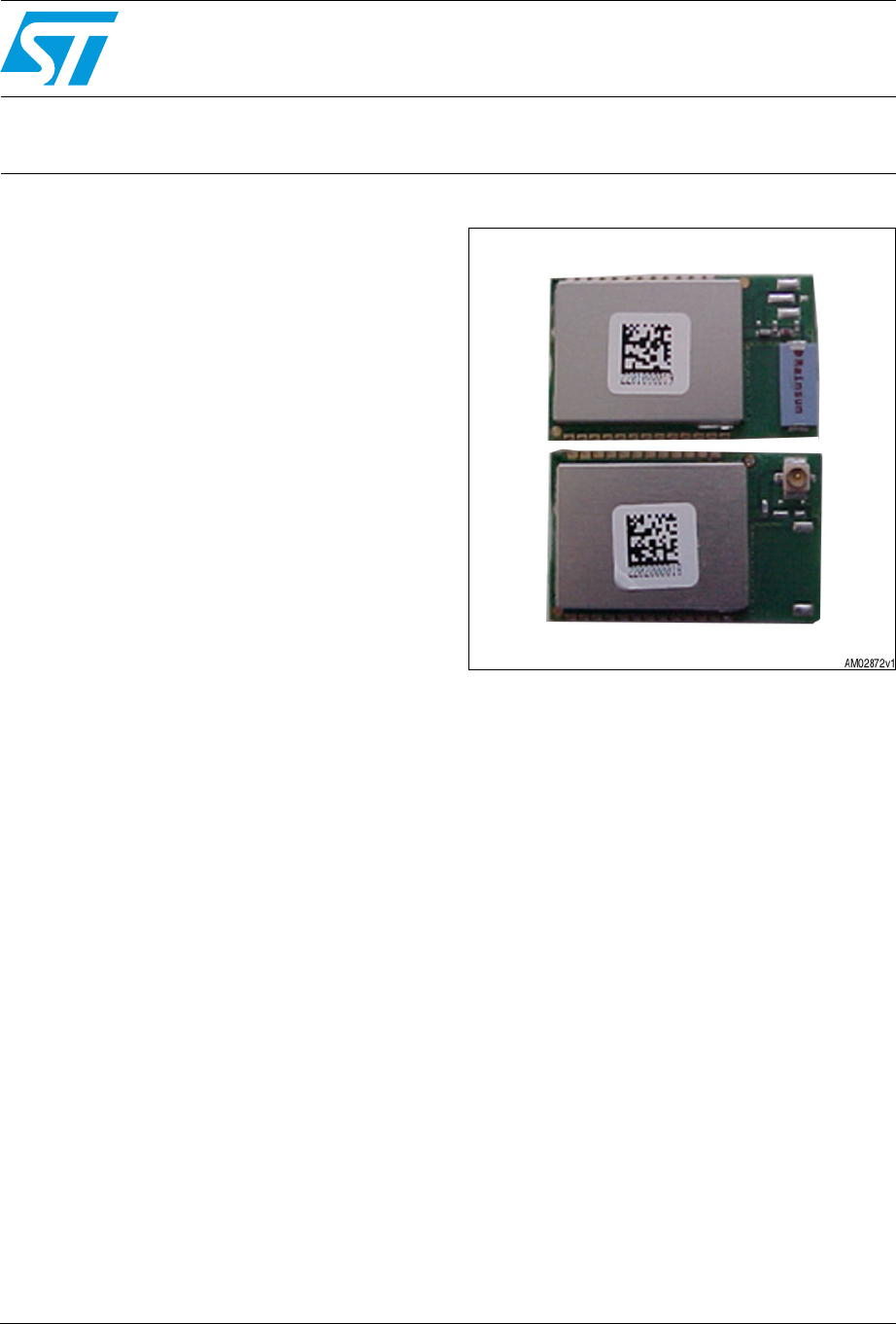
The series groups multiple versions that differ in terms of memory size , antenna (ceramic
antenna or integrated u.fl connector for the connection of an external antenna) and stacks
options (ZigBee, RF4CE, SimpleMAC).
The SPZB32W1y1.z versions are based on the STM32W108CB chipset integrating 128 kB
of embedded flash memory and 8 kB of RAM available for data and program storage.
For technical details on the STM32W108CB chipset refer to the related datasheet. For
technical details on the supported stacks refer to the related user guide and application
notes.

DRAFT
RoHS compliance SPZB32Wxy1.z
4/19 Doc ID xxxxx Rev 1
2 RoHS compliance
ST modules are RoHS compliant and comply with ECOPACK® norms.
3 Application
●Smart energy applications
●Machine2Machine industrial control
●Wireless sensor networks
●Home/building automation
●Smart appliances
●Wireless alarms and security systems
●Lighting control
●Remote monitoring
SPZB32Wxy1.z Block diagram
Doc ID xxxxx Rev 1 5/19
DRAFT
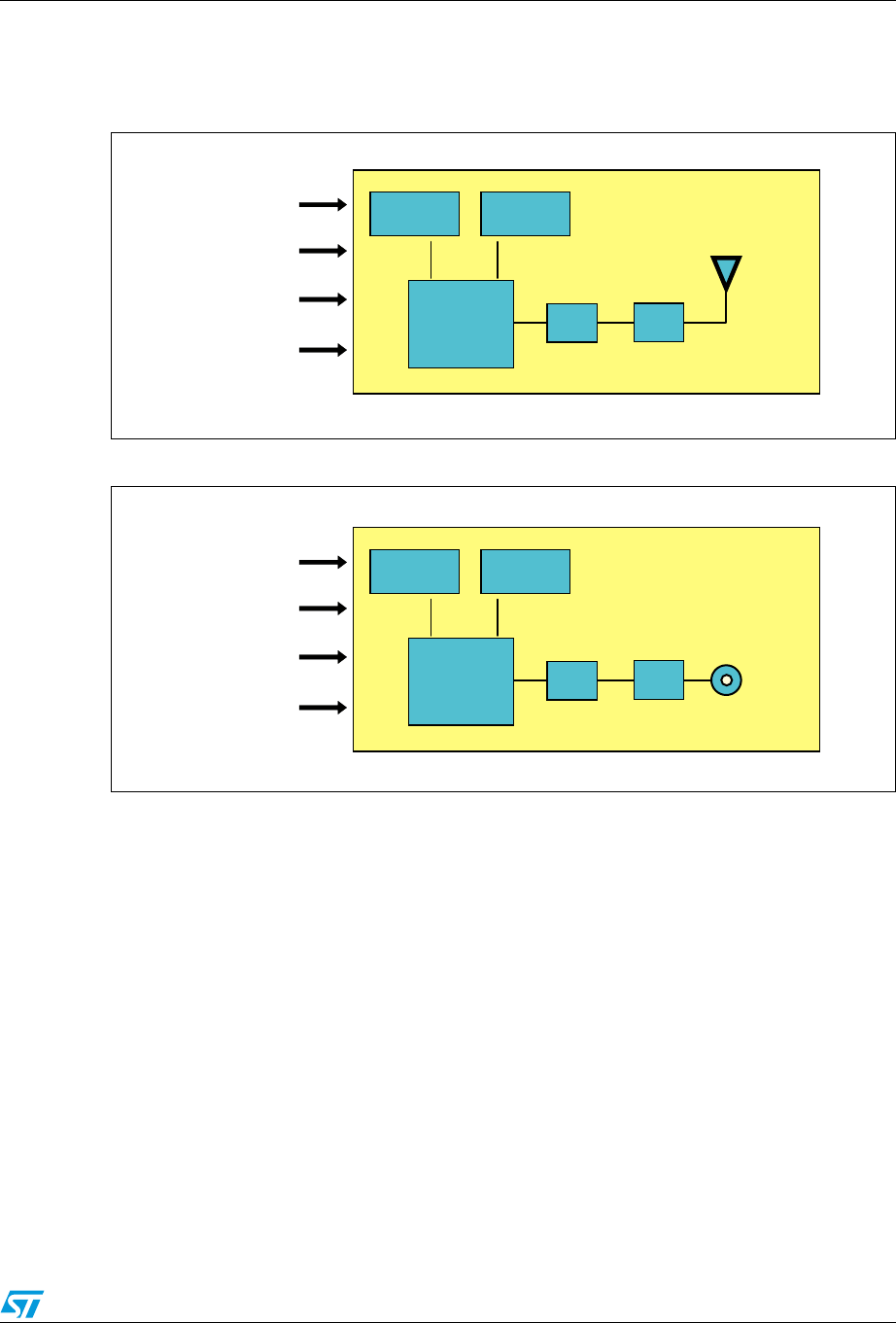
4 Block diagram
Figure 1. SPZB32WxA1.z block diagram
Figure 2. SPZB32WxC1.z block diagram
- (Z
8TAL
34- 73OC
6DD
*TAG
'0)/S
3YSTEM3IGNALS
2&
ANTENNA
K(Z
8TAL
"0&
".W
,.!
0!
- (Z
8TAL
34- 73O#
6DD
*TAG
'0)/S
3YSTEM3IGNALS
5&)
#ONNECTOR
K(Z
8TAL
"0&
".W
,.!
0!
DRAFT
Pin settings SPZB32Wxy1.z
6/19 Doc ID xxxxx Rev 1
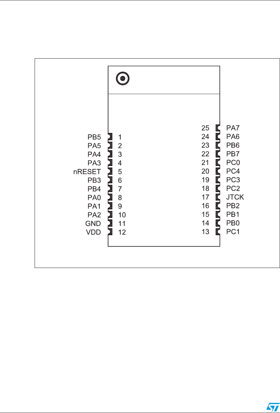
5 Pin settings
5.1 Pin connections
Figure 3. Pin connection diagram
TOP VIEW
Antenna
AM09235V1

DRAFT
SPZB32Wxy1.z Pin settings
Doc ID xxxxx Rev 1 7/19
5.2 Pin description
Table 1. Pin description
Module pin n° Pin name Direction STM32W pin Description
1
PB5 I/O 43 Digital I/O
ADC0 Analog 43 ADC Input 0
TIM2CLK I 43 Timer 2 external clock input
TIM1MSK I 43 Timer 1 external clock mask input
2
PA5 I/O 27 Digital I/O
ADC5 Analog 27 ADC Input 1
PTI_DATA O 27 Frame signal of PTI (Packet Trace Interface)
nBOOTMODE I 27 Embedded serial bootloader activation out of reset
TRACEDATA3 0 27 Synchrounus CPU trace data bit 3
3
PA4 I/O 26 Digital I/O
ADC4 Analog 26 ADC Input 0
PTI_EN O 26 Frame signal of PTI (Packet Trace Interface)
TRACEDATA2 O 26 Synchrounus CPU trace data bit 2
4
PA3 I/O 25 Digital I/O
SC2nSSEL I 25 SPI SLAVE SELECT of Serial Controller 2
TIM2_CH2 I/O 25 Timer 2 channel 2 output (or input - Disable remap with TIM2_OR[5])
TRACECLK O 25 Synchrounus CPU trace clock
5 nRESET I 12 Active low reset ( an internal pull-up of 30 kohm typ. is provided)
6
PB3 I/O 19 Digital I/O
UART_CTS I 19 UART CTS handshake of Serial Controller 1
SC1SCLK I/O 19 SPI slaver clock of Serial Controller SC1 / SPI master clock of Serial Controller SC1
TIM2_CH3 I/O 19 Timer 2 channel 3 input / Timer 2 channel 3 output

DRAFT
Pin settings SPZB32Wxy1.z
8/19 Doc ID xxxxx Rev 1
7
PB4 I/O 20 Digital I/O
UART_RTS O 20 UART RTS handshake of Serial Controller 1
TIM2_CH4 I/O 20 Timer 2 channel 4 input / Timer 2 channel 4 output
SC1nSSEL I 20 SPI slave select of Serial Controller 1
8
PA0 I/O 21 Digital I/O
SC2MOSI O 21 SPI Master data out of Serial Controller 2
SC2MOSI I 21 SPI Slave data in of Serial Controller 2
TIM2_CH1 I/O 21 Timer 2 channel 1 input / Timer 2 channel 1 output
9
PA1 I/O 22 Digital I/O
SC2MISO I 22 SPI Master data in of Serial Controller 2
SC2MISO O 22 SPI Slave data out of Serial Controller 2
SC2SDA I/O 22 TWI (I2C) data of Serial Controller 2
TIM2_CH3 I/O 22 Timer 2 channel 3 input / Timer 2 channel 3 output
10
PA2 I/O 24 Digital I/O
SC2SCLK O 24 SPI Master clock of Serial Controller 2
SC2SCLK I 24 SPI Slave clock of Serial Controller 2
SC2SCL I/O 24 TWI (I2C) clock of Serial Controller 2
TIM2_CH4 I/O 24 Timer 2 channel 4 input / Timer 2 channel 4 output
11 GND -- 49 Ground
12 VDD Power 16,23,28,37 Input power supply
13
PC1 I/O 38 Digital I/O
ADC3 Analog 38 ADC Input 3
SWO O 38 Serial Wire Output ayncronous trace output to debugger
TRACEDATA0 O 38 Syncronous CPU trace data bit 0
Table 1. Pin description (continued)
Module pin n° Pin name Direction STM32W pin Description

DRAFT
SPZB32Wxy1.z Pin settings
Doc ID xxxxx Rev 1 9/19
14
PB0 I/O 36 Digital I/O
VREF (O/I) Analog 36 ADC reference output / ADC reference input
TIM1CLK I 36 Timer 1 external clock input
TIM2MSK I 36 Timer 2 external clock mask input
IRQA I 36 External interrupt source A
TRACECLK O 36 Syncronous CPU trace clock
15
PB1 I/O 30 Digital I/O
SC1TXD O 30 UART transmit data of Serial Controller 1
SC1MOSI / SC1MISO O 30 SPI master data out of Serial Controller 1 / SPI slave data out of Serial Controller 1
SC1SDA I/O 30 TWI (I2C) data of Serial Controller 1
TIM2_CH1 I/O 30 Timer 2 channel 1 input / Timer 2 channel 1 output
16
PB2 I/O 31 Digital I/O
SC1RXD I 31 UART receive data of Serial Controller 1
SC1MISO / SC1MOSI I 31 SPI master data in of Serial Controller SC1 / SPI slave data in of Serial Controller 1
SC1SCL I/O 31 TWI (I2C) clock of Serial Controller 1
TIM2_CH2 I/O 31 Timer 2 channel 2 input / Timer 2 channel 2 output
17 JTCK I 32 JTAG clock input from debugger
SWCLK I/O 32 Serial Wire clock input/output with debugger
18
PC2 I/O 33 Digital I/O
JTDO O 33 JTAG data out to debugger
SWO O 33 Serial Wire Output asyncronous trace output to debugger
19 PC3 I/O 34 Digital I/O
JTDI I 34 JTAG data in from debugger
20
PC4 I/O 35 Digital I/O
JTMS I 35 JTAG mode select from debugger
SWDIO I/O 35 Serial Wire bidirectional data to/from debugger
Table 1. Pin description (continued)
Module pin n° Pin name Direction STM32W pin Description

DRAFT
Pin settings SPZB32Wxy1.z
10/19 Doc ID xxxxx Rev 1
21
PC0 I/O 40 Digital I/O (high current)
JRST I 40 JTAG reset input from debugger
TRACEDATA1 O 40 Syncronous CPU trace data bit 1
IRQD I 40 External interrupt source D
22
PB7 I/O 41 Digital I/O
TIM1_CH2 O 41 Timer 1 channel 2 output
TIM1 _CH2 I 41 Timer 1 channel 2 input
IRQC I 41 External interrupt source C
ADC2 I 41 ADC input 2
23
PB6 I/O 42 Digital I/O
TIM1_CH1 O 42 Timer 1 channel 1 output
TIM1_CH1 I 42 Timer 1 channel 1 input
IRQB I 42 External interrupt source B
ADC1 Analog 42 ADC input 1
24
LNA/ENABLE I 29
Digital input, module firmware dependent, externally forced by the user dedicated
firmware. This signal is dedicated to manage the SIGE-SE2432L internal LNA.
(HIGH= internal LNA enabled, LOW= internal LNA disabled).
PA6/LNA_ENABLE O 29
Digital output, module firmware dependent, internally forced by application dedicated
firmware. This signal is dedicated to manage the SIGE-SE2432L internal LNA. (HIGH=
internal LNA enabled, LOW= internal LNA disabled).
25
RF_STANDBY I 18
Digital input, module firmware dependent, externally forced by the user dedicated
firmware. This signal is dedicated to manage the SIGE-SE2432L front-end STANDBY
state.
(HIGH= Front-end enabled, LOW= Front-end forced in the STANDBY state).
PA7/RF_STANDBY O 18
Digital output, module firmware dependent, internally forced by application dedicated
firmware. This signal is dedicated to manage the SIGE-SE2432L front-end STANDBY
state.
(HIGH= Front-end enabled, LOW= Front-end forced into STANDBY state).
Table 1. Pin description (continued)
Module pin n° Pin name Direction STM32W pin Description

SPZB32Wxy1.z Electrical characteristics
Doc ID xxxxx Rev 1 11/19
DRAFT
6 Electrical characteristics
6.1 Absolute maximum ratings
6.2 Recommended operating conditions
6.3 DC electrical characteristics
Table 2. Absolute maximum ratings
Symbol Parameter Min. Max. Unit
VDD Module supply voltage - 0.3 3.6 V
Vin Input voltage on any digital pin - 0.3 Vdd + 0.3 V
Tstg Storage temperature -40 +85 °C
Tsold Soldering temperature < 10s 250 °C
Table 3. Recommended operating conditions
Symbol Parameter Conditions Min. Typ. Max. Unit
VDD Module supply voltage -40 °C < T < +85 °C 2.1 3.3 3.6 V
Tstg Operating ambient temperature -40 +85 °C
Table 4. DC electrical characteristics
Symbol Parameter Conditions Min. Typ. Max. Unit
IRX RX current Vdd = 3.3 V, T= 25 °C - 20 - mA
ITX TX current Po = 18 dBm, Vdd = 3.3 V,
T = 25 °C, F = 2450MHz -120 - mA
IDS Deep sleep current
(32.768 kHz oscillator) Vdd = 3.3 V, T = 25 °C - 1.3 - mA
DRAFT
Electrical characteristics SPZB32Wxy1.z
12/19 Doc ID xxxxx Rev 1
6.4 Digital I/O specifications
6.5 RF electrical characteristics
Table 5. Digital I/O specifications
Symbol Parameter Conditions Min. Typ. Max. Unit
VIL Low level input voltage 2.1 < Vdd < 3.6 V 0 0.5 x Vdd V
VIH High level input voltage 2.1 < Vdd < 3.6 V 0.62 x Vdd Vdd V
Iil Input current for logic 0 2.1 < Vdd < 3.6 V -0.5 mA
Iih Input current for logic 1 2.1 < Vdd < 3.6 V 0.5 mA
Ripu Input pull-up resistor 30 kΩ
Ripd Input pull-down resistor 30 kΩ
VOL Low level output voltage 0 0.18 x Vdd V
VOH High level output voltage 0.82 x Vdd Vdd V
IOHS Output source current (standard) 4 mA
IOLS Output sink current (standard) 4 mA
IOHH Output source current (high current) 8 mA
IOLH Output sink current (high current) 8 mA
IOTot Total output current for I/O 40 mA
Table 6. Electrical characteristics
Symbol Parameter Conditions Min. Typ. Max. Unit
Frequency range Vdd = 3.3 V, T= 25 °C 2405 2480 MHz
TX Output power Vdd = 3.3 V, T= 25 °C 20 dBm
RX Sensitivity Vdd = 3.3 V, 1 % PER -105 dBm
Adjacent channel rejection ±5 MHz
±10 MHZ
35
40 dBm
SPZB32Wxy1.z Mechanical dimensions
Doc ID xxxxx Rev 1 13/19
DRAFT
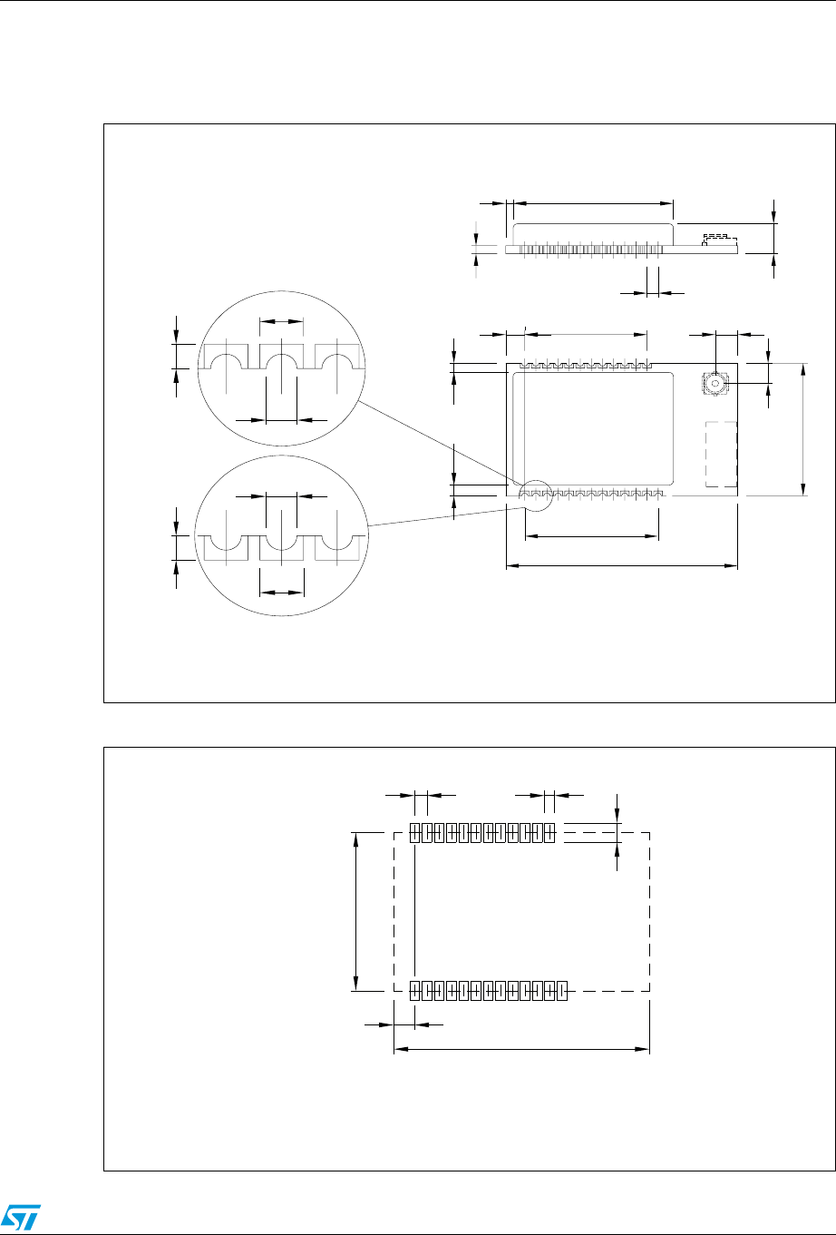
7 Mechanical dimensions
Figure 4. Mechanical dimensions
Figure 5. Pin land pattern (dimensions in mm)
[
SLWFK PP
7ROHUDQFHV PP
%277209,(:
6FDOH
7239,(:
$QWHQQD
[
5(&200(1'('
/$1'
3$77(51
723
9,(:
SLWFK
!-6
DRAFT
Soldering SPZB32Wxy1.z
14/19 Doc ID xxxxx Rev 1
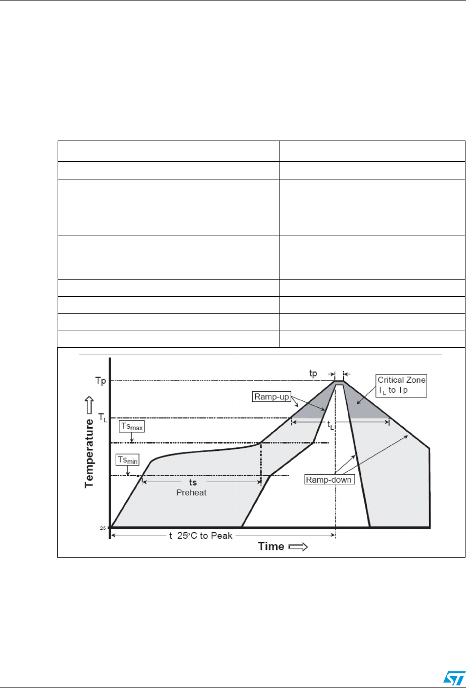
8 Soldering
The soldering phase must be carefully executed; in order to avoid undesired melting
phenomenon, particular attention must be paid to the set-up of the peak temperature.
Below are some suggestions for the temperature profile based on IPC/JEDEC J-STD-020C,
July 2004 recommendations
Table 7. Soldering
Profile feature PB free assembly
Average ramp up rate (TSMAX to TP) 3 °C / sec max.
Preheat
Temperature min. (TS MIN)
Temperature max. (TS MAX)
Time (TS MIN to TS MAX) (tS)
150 °C
200 °C
60 – 100 sec
Time maintained above:
Temperature TL
Time tL
217 °C
40 – 70 sec
Peak temperature (Tp)240 + 0 °C
Time within 5 °C of actual peak temperature (tP) 10 – 20 sec
Ramp down rate 6 °C / sec
Time from 25 °C to peak temperature 8 minutes max.

SPZB32Wxy1.z Product approvals
Doc ID xxxxx Rev 1 15/19
DRAFT
9 Product approvals
This series of modules has been designed to meet national regulations for world wide use.
Different versions of modules belonging to the same series are orderable as it is specified in
the Section 10. They differ in terms of integrated memory size and protocol stack enabled
to run while sharing the same manufacturing , design and radios capabilities. As
representative of the series from the RF design and radios capabilities, the versions using
128 kB Flash/8kB RAM and Zigbee PRO Protocol stack (i.e. SPZB32W1A1.1 and
SPZB32W1C1.1) have been used during the certification tests. The following certifications
have been obtained.
9.1 FCC approvals
The SPZB32W1A1.1 device, with integrated antenna, as well as the SPZB32W1C1.1, with
the antenna specified in Ta b l e 8 , have been tested and found to comply with the limits for a
Class B digital device , pursuant to part 15 of the FCC rules. These limits are designed to
provide reasonable protection against harmful interference in a residential installation.
This equipment generates, uses and can radiate radio frequency energy and, if not installed
and used in accordance with the instructions, may cause harmful interference to radio
communications.
However, there is no guarantee that interference will not occur in a particular installation. If
this equipment does cause harmful interference to radio or television reception, which can
be determined by turning the equipment off and on, the user is encouraged to try to correct
the interference by one or more of the following measures:
●Reorient or relocate the receiving antenna
●Increase the separation between the equipment and receiver
●Connect the equipment into an outlet on a circuit different from that to which the
receiver is connected
Consult the dealer or an experienced radio/TV technician for help
Module type: ZigBee® module SPZB32W1A1.1 / SPZB32W1C1.1
FCC-ID: S9NZB32C1
Modular type: single modular
Any changes or modifications not expressed approved by the part responsible for
compliance could cause the module to cease to comply with FCC rules part 15, and thus
void the user’s authority to operate the equipment.
While the applicant for a device into which the SPZB32W1A1.1 or the SPZB32W1C2.1 with
the antenna specified in Ta b l e 8 installed is not required to obtain new authorization for the
module, this does not preclude the possibility that some other form of authorization or
testing may be required for the end product.
Table 8. Antenna used for FCC approvals
ITEM Part N° Manufacturer
1 2010B4844-01 (Titanis Antenna) Antenova
DRAFT
Product approvals SPZB32Wxy1.z
16/19 Doc ID xxxxx Rev 1
9.1.1 FCC labeling requirements
When integrating the SPZB32W1A1.1 / SPZB32W1C1.1 into the final product, il must be
ensured that the FCC labelling requirements, as specified below, are satisfied.
Based on the Public Notice from FCC, the product into which our transmitter module is
installed must display a label referring to the enclosed module.
The label should use wording such as “Contains Transmitter module FCC ID: S9NZB32C1
or “Contains FCC ID: S9NZB32C1” , any similar wording that expressed the same meaning
may be used.
An example is:
Contains FCC ID: S9NZB32C1
9.2 European certification
SPZB32W1A1.1 and SPZB32W1C2.1 devices are CE certified:
Expert opinion N. xxx-xxxxxx released by IMQ refers to the following normative:
Radio: EN300 328: V1.7.1:2006-10
EMC: EN301 489 17 V2.1.1:2009
Safety: EN60950-1:2006 + A11:2009
0051

SPZB32Wxy1.z Ordering information scheme
Doc ID xxxxx Rev 1 17/19
DRAFT
10 Ordering information scheme
Note: Check availability of the different versions with your ST sales representative.
Table 9. Ordering information scheme
SPZB 32Wx y 1 .z
802.15.4 / ZigBee modules
Memory options:
x --> 1: 128 kB Flash; 8 kB RAM
x --> 2: 256 kB Flash; 16 kB RAM
Antenna options:
y --> A: Integrated ceramic antenna
y --> C: Integrated UFL connector
1: Long TX range
Firmware options:
z --> 1: ZigBee PRO (EmberZnet)
z --> 2: STM ZigBee
z --> 3: RF4CE
z --> 4: SimpleMAC
z --> 5: Zigbee IP

DRAFT
Revision history SPZB32Wxy1.z
18/19 Doc ID xxxxx Rev 1
11 Revision history
Table 10. Document revision history
Date Revision Changes
28-Jul-2011 1 Initial release

SPZB32Wxy1.z
Doc ID xxxxx Rev 1 19/19
DRAFT
Please Read Carefully:
Information in this document is provided solely in connection with ST products. STMicroelectronics NV and its subsidiaries (“ST”) reserve the
right to make changes, corrections, modifications or improvements, to this document, and the products and services described herein at any
time, without notice.
All ST products are sold pursuant to ST’s terms and conditions of sale.
Purchasers are solely responsible for the choice, selection and use of the ST products and services described herein, and ST assumes no
liability whatsoever relating to the choice, selection or use of the ST products and services described herein.
No license, express or implied, by estoppel or otherwise, to any intellectual property rights is granted under this document. If any part of this
document refers to any third party products or services it shall not be deemed a license grant by ST for the use of such third party products
or services, or any intellectual property contained therein or considered as a warranty covering the use in any manner whatsoever of such
third party products or services or any intellectual property contained therein.
UNLESS OTHERWISE SET FORTH IN ST’S TERMS AND CONDITIONS OF SALE ST DISCLAIMS ANY EXPRESS OR IMPLIED
WARRANTY WITH RESPECT TO THE USE AND/OR SALE OF ST PRODUCTS INCLUDING WITHOUT LIMITATION IMPLIED
WARRANTIES OF MERCHANTABILITY, FITNESS FOR A PARTICULAR PURPOSE (AND THEIR EQUIVALENTS UNDER THE LAWS
OF ANY JURISDICTION), OR INFRINGEMENT OF ANY PATENT, COPYRIGHT OR OTHER INTELLECTUAL PROPERTY RIGHT.
UNLESS EXPRESSLY APPROVED IN WRITING BY AN AUTHORIZED ST REPRESENTATIVE, ST PRODUCTS ARE NOT
RECOMMENDED, AUTHORIZED OR WARRANTED FOR USE IN MILITARY, AIR CRAFT, SPACE, LIFE SAVING, OR LIFE SUSTAINING
APPLICATIONS, NOR IN PRODUCTS OR SYSTEMS WHERE FAILURE OR MALFUNCTION MAY RESULT IN PERSONAL INJURY,
DEATH, OR SEVERE PROPERTY OR ENVIRONMENTAL DAMAGE. ST PRODUCTS WHICH ARE NOT SPECIFIED AS "AUTOMOTIVE
GRADE" MAY ONLY BE USED IN AUTOMOTIVE APPLICATIONS AT USER’S OWN RISK.
Resale of ST products with provisions different from the statements and/or technical features set forth in this document shall immediately void
any warranty granted by ST for the ST product or service described herein and shall not create or extend in any manner whatsoever, any
liability of ST.
ST and the ST logo are trademarks or registered trademarks of ST in various countries.
Information in this document supersedes and replaces all information previously supplied.
The ST logo is a registered trademark of STMicroelectronics. All other names are the property of their respective owners.
© 2011 STMicroelectronics - All rights reserved
STMicroelectronics group of companies
Australia - Belgium - Brazil - Canada - China - Czech Republic - Finland - France - Germany - Hong Kong - India - Israel - Italy - Japan -
Malaysia - Malta - Morocco - Philippines - Singapore - Spain - Sweden - Switzerland - United Kingdom - United States of America
www.st.com