ST Microelectronics S R L ZB32C2 ZigBee Module User Manual
ST Microelectronics S.R.L. ZigBee Module
UserManual.wiki
>
ST Microelectronics S R L
>
ZB32C2 User Manual
User manual
Navigation menu
Upload a User Manual
Namespaces
Wiki Guide
HTML
PDF
Info
Views
User Manual
Discussion / Help
Navigation
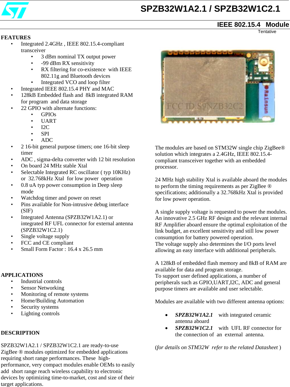
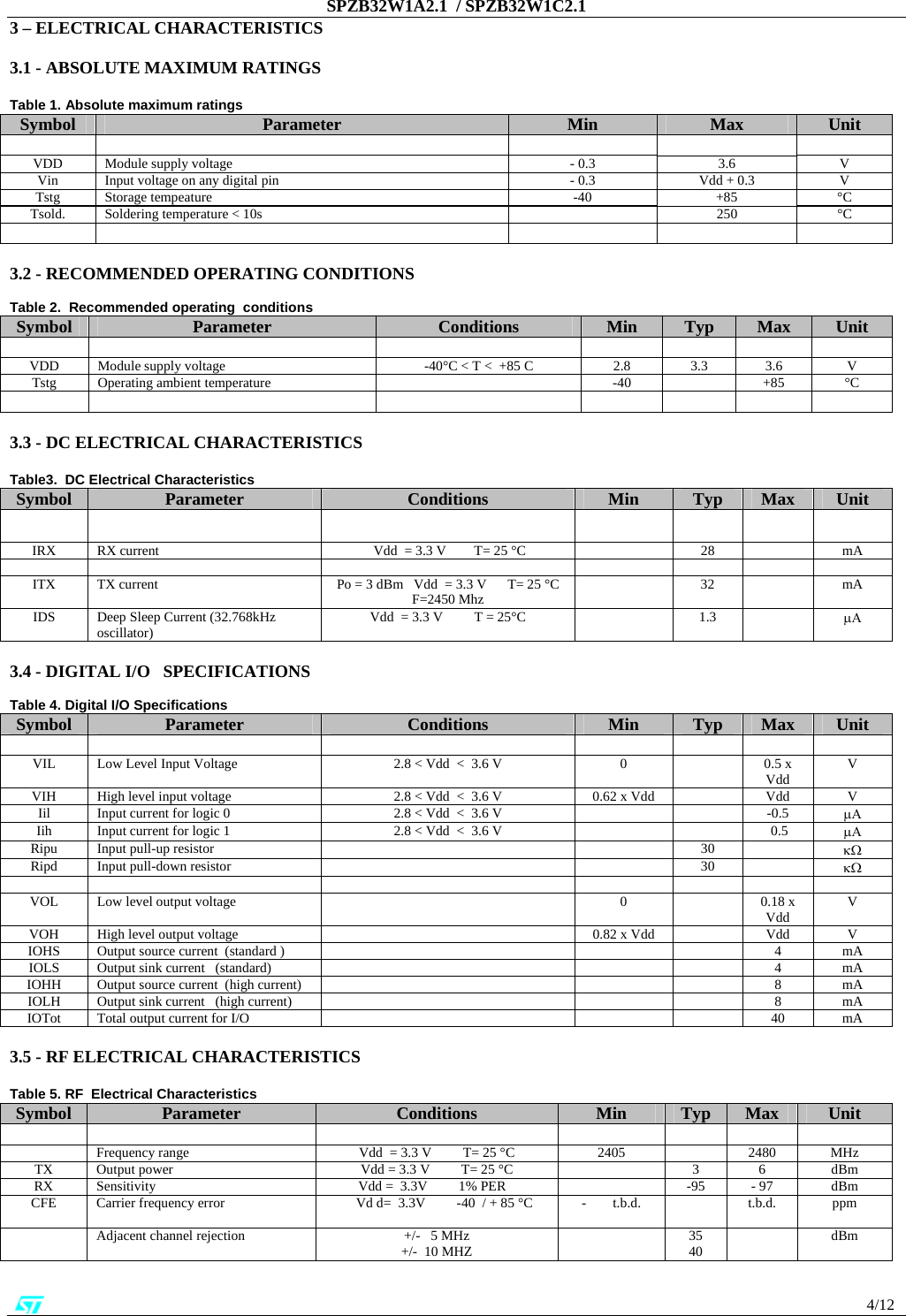
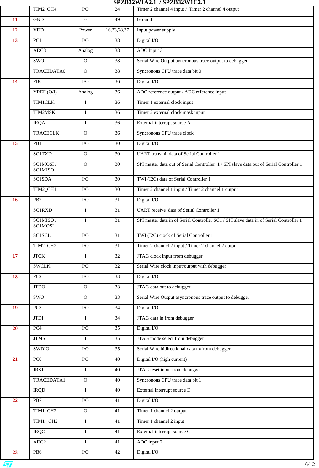
![SPZB32W1A2.1 / SPZB32W1C2.1 5/12 4 – PIN DESCRIPTION Table 6. Pin Description Module Pin Number PIN Name Direction STM32W pin Description 1 PB5 I/O 43 Digital I/O ADC0 Analog 43 ADC Input 0 TIM2CLK I 43 Timer 2 external clock input TIM1MSK I 43 Timer 1 external clock mask input 2 PA5 I/O 27 Digital I/O ADC5 Analog 27 ADC Input 1 PTI_DATA O 27 Frame signal of PTI (Packet Trace Interface) nBOOTMODE I 27 Embedded serial bootloader activation out of reset TRACEDATA3 0 27 Synchrounus CPU trace data bit 3 3 PA4 I/O 26 Digital I/O ADC4 Analog 26 ADC Input 0 PTI_EN O 26 Frame signal of PTI (Packet Trace Interface) TRACEDATA2 O 26 Synchrounus CPU trace data bit 2 4 PA3 I/O 25 Digital I/O SC2nSSEL I 25 SPI SLAVE SELECT of Serial Controller 2 TIM2_CH2 I/O 25 Timer 2 channel 2 output (or input - Disable remap with TIM2_OR[5]) TRACECLK O 25 Synchrounus CPU trace clock 5 nRESET I 12 Active low reset ( an internal pull-up of 30 kohm typ. is provided) 6 PB3 I/O 19 Digital I/O UART_CTS I 19 UART CTS handshake of Serial Controller 1 SC1SCLK I/O 19 SPI slaver clock of Serial Controller SC1 / SPI master clock of Serial Controller SC1 TIM2_CH3 I/O 19 Timer 2 channel 3 input / Timer 2 channel 3 output 7 PB4 I/O 20 Digital I/O UART_RTS O 20 UART RTS handshake of Serial Controller 1 TIM2_CH4 I/O 20 Timer 2 channel 4 input / Timer 2 channel 4 output SC1nSSEL I 20 SPI slave select of Serial Controller 1 8 PA0 I/O 21 Digital I/O SC2MOSI O 21 SPI Master data out of Serial Controller 2 SC2MOSI I 21 SPI Slave data in of Serial Controller 2 TIM2_CH1 I/O 21 Timer 2 channel 1 input / Timer 2 channel 1 output 9 PA1 I/O 22 Digital I/O SC2MISO I 22 SPI Master data in of Serial Controller 2 SC2MISO O 22 SPI Slave data out of Serial Controller 2 SC2SDA I/O 22 TWI (I2C) data of Serial Controller 2 TIM2_CH3 I/O 22 Timer 2 channel 3 input / Timer 2 channel 3 output 10 PA2 I/O 24 Digital I/O SC2SCLK O 24 SPI Master clock of Serial Controller 2 SC2SCLK I 24 SPI Slave clock of Serial Controller 2 SC2SCL I/O 24 TWI (I2C) clock of Serial Controller 2](https://usermanual.wiki/ST-Microelectronics-S-R-L/ZB32C2/User-Guide-1373151-Page-5.png)