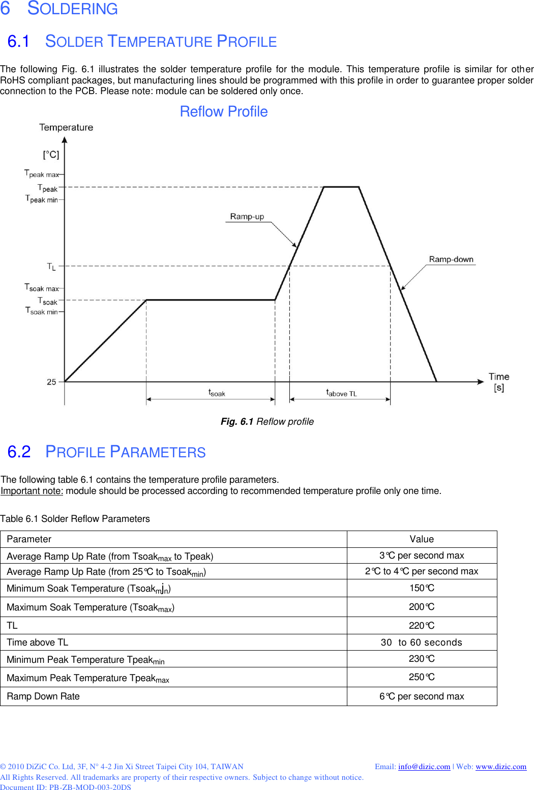
STMicroelectronicsS DZSTM32WA DZ-SB-S-A Zigbee Module User Manual DiZiC ZigBee Modules
STMicroelectronics DZ-SB-S-A Zigbee Module DiZiC ZigBee Modules
UserManual.wiki
>
STMicroelectronicsS
>
DZSTM32WA User Manual
>
manual
Contents
1.
manual
2.
chip antenna datasheet
manual
Navigation menu
Upload a User Manual
Namespaces
Wiki Guide
HTML
PDF
Info
Views
User Manual
Discussion / Help
Navigation
![© 2010 DiZiC Co. Ltd, 3F, N° 4-2 Jin Xi Street Taipei City 104, TAIWAN Email: info@dizic.com | Web: www.dizic.com All Rights Reserved. All trademarks are property of their respective owners. Subject to change without notice. Document ID: PB-ZB-MOD-003-20DS 802.15.4 Family of RF Modules High Performance and Long Range 802.15.4 STM32W RF Modules Quickly add wireless capability with these high performance ZigBee compliant modules READY TO USE SoC RF MODULES Quickly add wireless networking capabilities to your products with these ready-to-use DiZiC 802.15.4 RF Modules. Simple to operate and available in a wide range of configurations, these ZigBee compliant RF modules are ideal for industrial sensors, consumer remote controls, home appliances, and more. Based on the STM32W108 wireless System-on-Chip (SoC) from STMicroelectronics, this family of modules offer outstanding RF performance with a -99 dBm normal RX sensitivity (configurable to -100 dBm) and +3 dBm normal mode output power (configurable up to +7 dBm). With a small form factor and pin-to-pin compatible, DiZiC 802.15.4 RF Modules are available with several software stack options, including EmberZNet PRO, RF4CE stack, or proprietary low level MAC / PHY stack. VERSATILE CONFIGURATIONS With several possible configurations, select from 3 power level options, 3 output options, 3 software stack options and 2 EMI options: Power Level Options - Choose from a standard power level (+7 dBm), and two versions of RF front end (PA and LNA, +20 dBm). RF Output Options - Choose from a chip antenna, a U.FL connector, or a single port 50 Ohm RF pad. The U.FL connector allows, amongst other uses, for connecting an external antenna, for connecting to an application board that provides additional filters, or for connecting to another 50 Ohm coaxial cable TX line. The single port 50 Ohm RF pad allows for a direct connection to another board, application module, or external antenna. Software Stack Options - Choose from EmberZNet PRO, RF4CE, or a low level PHY / MAC stack. EmberZNet PRO is an easy to use ZigBee platform for complex mesh networks. RF4CE (Radio Frequency for Consumer Electronics) is a new protocol for consumer remote controlled equipment. Custom applications can be developed on top of a simple to use and low footprint PHY/MAC API library. EMI Options – Choose metal shielding protection where enhanced electromagnetic interference immunity is required otherwise standard version without metal shielding is advisable. D/Z/C 802.15.4 STM32WRF Module with RF front end and antenna Key Features • STM32W108 ZigBee / IEEE 802.15.4 SoC • 32-bit ARM Cortex-M3 processor • 128 kB of Flash and 8 kB of SRAM • JTAG / SWD (programming and debugging) • 2.4 GHz ISM supporting 16 channels • Data rate up to 250 kbit/s • 128-bit AES encryption • Peripherals • 24 GPIOs, SPI, USART, and I2C • 12-bit ADC with up to 6 inputs • 2x 16-bit timers • DMA controller • Standard module • RX Sensitivity -99 dBm (-100 dBm Boost) • TX Power 3 dBm (+7 dBm Boost) • RF front end options • Two Front End options • Both with RX Sensitivity -105 dBm • Both with TX Power +20 dBm • RF Options • Chip antenna, U.FL connector, or single port 50 Ohm RF pad • Shielding option for enhanced EMI protection Ordering Information DZ_ZB_[P] [O] [S][E] , where: [P] Power level options, one of: S (standard +7 dBm), R (Front End with Power Level Detect +20 dBm), or T (Front End +20 dBm) [O] Output options, one of: A (Embedded SMD antenna assembled on module), P (Single ended 50 Ohm. RF Pad), or U (50 Ohm U.FL coaxial connector) [S] Stack options, one of: F (RF4CE stack), X (Proprietary stack), or Z (EmberZNet PRO stack) [E] EMI protection options, one of: S (standard, no shielding), or M (enhanced, with metal shield)](https://usermanual.wiki/STMicroelectronicsS/DZSTM32WA.manual/User-Guide-1313171-Page-1.png)
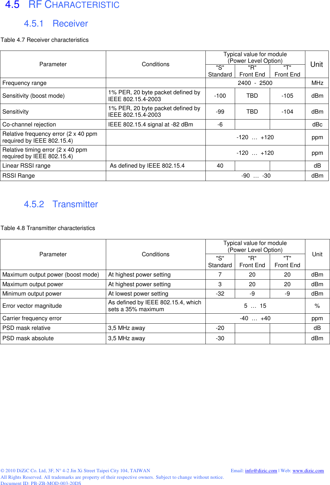
![© 2010 DiZiC Co. Ltd, 3F, N° 4-2 Jin Xi Street Taipei City 104, TAIWAN Email: info@dizic.com | Web: www.dizic.com All Rights Reserved. All trademarks are property of their respective owners. Subject to change without notice. Document ID: PB-ZB-MOD-003-20DS DIZIC 802.15.4 RF MODULE DZ-ZB-[P]-[O]-[S]-[E] DATA SHEET POWER LEVEL OPTIONS STANDARD FRONT END FRONT END WITH RF POWER LEVEL DETECTOR 1 FEATURE LISTComplete System-on-Chip • 32-bit ARM® Cortex-M3 processor • 2.4 GHz IEEE 802.15.4 transceiver & lower MAC • 128 kB flash, 8kB RAM memory • AES128 encryption accelerator • Flexible ADC, SPI/UART/TWI serial communications, and general purpose timers • 24 highly configurable GPIO with Schmitt trigger inputs Industry-leading ARM Cortex-M3 processor • Leading 32-bit processing performance • Highly efficient Thumb-2 instruction set • Operation at 6, 12 or 24 MHz • Flexible Nested Vectored Interrupt Controller Low power consumption, advanced management • RX Current (w/ CPU): 27 mA • TX Current (w/ CPU, +3 dBm TX): 31 mA • Low deep sleep current, with retained RAM and GPIO: 400 nA/800 nA with/without sleep timer • Low-frequency internal RC oscillator for low-power sleep timing • High-frequency internal RC oscillator for fast (100 µsec) processor start-up from sleep Innovative network and processor debug • Serial Wire/JTAG interface • Standard ARM debug capabilities: Flash Patch & Breakpoint; Data Watch-point & Trace; Instrumentation Trace MacrocellExceptional RF Performance • Normal mode Link Budget up to 102 dB; configurable up to107dB • -99 dBm normal RX sensitivity; configurable to -100 dBm (1%PER, 20 byte packet) • +3 dB normal mode output power; configurable up to +7 dBm • Robust WiFi and Bluetooth coexistence Application Flexibility • Single voltage operation: 2.1-3.6 V • Optional 32.768 kHz crystal for higher timer accuracy • Low external component count with single 24 MHz crystal • External power amplifier versions Target applications for the Modules include: • Smart Energy • Building automation and control (HVAC) • Home automation and control • Security and monitoring • AMR/AMI • Logistic & Asset tracking • Medical • General ZigBee wireless sensor networking • Active RFID • Wireless handheld terminals • Industry telemetry and automatic data collection system • Temperature and humidity control system • Traffic and control for street lamp](https://usermanual.wiki/STMicroelectronicsS/DZSTM32WA.manual/User-Guide-1313171-Page-3.png)
![© 2010 DiZiC Co. Ltd, 3F, N° 4-2 Jin Xi Street Taipei City 104, TAIWAN Email: info@dizic.com | Web: www.dizic.com All Rights Reserved. All trademarks are property of their respective owners. Subject to change without notice. Document ID: PB-ZB-MOD-003-20DS 2 MODULE VARIANTS 2.1 INTRODUCTION The DZ-ZB is low-power, high sensitivity IEEE 802.15.4 / ZigBee-compliant module. This multi-functional device based on STMicroelectronics STM32W108 fully integrated System-on-Chip [1]. The STM32W108 integrates a 2.4 GHz, IEEE 802.15.4-compliant transceiver, 32-bit ARM® Cortex™-M3 microprocessor, Flash and RAM memory, and peripherals of use to designers of ZigBee-based systems [2]. Block diagrams of DZ-ZB Module is show on Figure 2.1 and utilizes STM32W108CBU6x version of the high performance, IEEE 802.15.4 compliant, wireless system-on-chip STM32W108 family. Fig. 2.1 Block diagram of DZ-ZB Modules DZ-ZB modules are available in two different product lines: without/with PA/LNA Front-End (FE). Both product lines offering three ZigBee stack configurations. The first decision you need to make is if you want the Output option. The following options are available: A - Embedded SMD Antenna P - Single ended 50 Ohm RF Pad U - U.FL 50 Ohm coaxial connector The second decision you need to make is Power level option. The following options are available: S - Standard + 7dBm R - Front End (PA and LNA) with RF output power level detector + 20 dBm T - Front End (PA and LNA) + 20 dBm The third decision you need to make ZigBee stack. The following options are available: F - RF4CE stack X - Proprietary stack Z - EmberZnet PRO stack The final decision is level of electromagnetic immunity (EMI) protection. The following options are available: M - Metal cap shielding enabling enhanced level of electromagnetic immunity (EMI) protection S - Standard, without metal shielding cap The next chapters will explain each of all options. 2.2 DIZIC 802.15.4 RF MODULE: OUTPUT OPTIONS The following Output Options are available: A - Embedded SMD Antenna P - Single ended 50 Ohm RF Pad U - U.FL 50 Ohm coaxial connector](https://usermanual.wiki/STMicroelectronicsS/DZSTM32WA.manual/User-Guide-1313171-Page-4.png)
![© 2010 DiZiC Co. Ltd, 3F, N° 4-2 Jin Xi Street Taipei City 104, TAIWAN Email: info@dizic.com | Web: www.dizic.com All Rights Reserved. All trademarks are property of their respective owners. Subject to change without notice. Document ID: PB-ZB-MOD-003-20DS 2.3 DIZIC 802.15.4 RF MODULE: POWER LEVEL OPTIONS The following Power Level Options are available: Option S - Standard + 7dBm STM32W chip: System on Chip - where radio, microcontroller, program/user memory, RAM, ZigBee protocols stack are integrated in one chip. Option R - Front End (PA and LNA) with RF output power level detector + 20 dBm STM32W chip: System on Chip - where radio, microcontroller, program/user memory, RAM, ZigBee protocols stack are integrated in one chip. Option T - Front End (PA and LNA) + 20 dBm STM32W chip: System on Chip - where radio, microcontroller, program/user memory, RAM, ZigBee protocols stack are integrated in one chip. 2.4 DIZIC 802.15.4 RF MODULE: STACK OPTIONS The following ZigBee stack options are available: Option F - RF4CE stack Option X - Proprietary stack Option Z - EmberZnet PRO stack Instructions concerning to programming ST32W108 you will find at [7] and examples of Application at [6]. 2.5 DIZIC 802.15.4 RF MODULE: EMI PROTECTION OPTIONS The following EMI protection options are available: Option M - Metal shield cap enabling enhanced level of electromagnetic immunity (EMI) protection Option S - Standard module without metal shielding](https://usermanual.wiki/STMicroelectronicsS/DZSTM32WA.manual/User-Guide-1313171-Page-5.png)
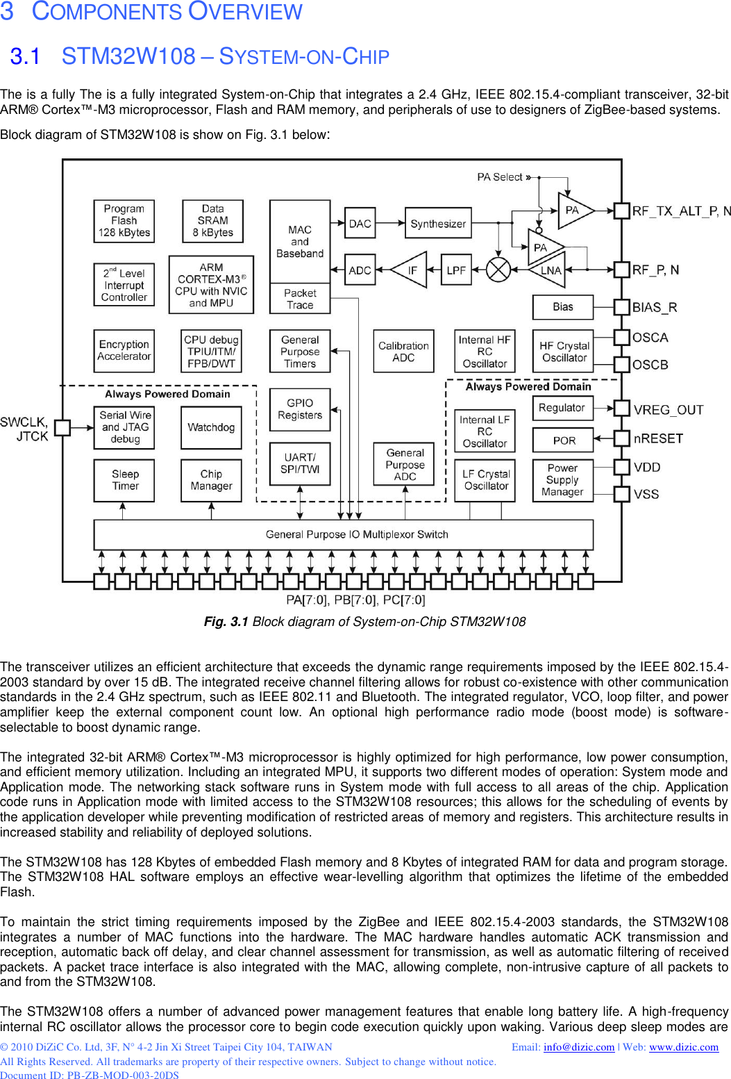
![© 2010 DiZiC Co. Ltd, 3F, N° 4-2 Jin Xi Street Taipei City 104, TAIWAN Email: info@dizic.com | Web: www.dizic.com All Rights Reserved. All trademarks are property of their respective owners. Subject to change without notice. Document ID: PB-ZB-MOD-003-20DS 3.3 RF FRONT END This is a cost-effective and high performance RF Front End for low-power and low-voltage 2.4-GHz wireless applications. It is a range extender for all existing and future 2.4-GHz low-power RF transceivers, transmitters and System-on-Chip products. It increases the link budget by providing a power amplifier for increased output power, and an LNA with low noise figure for improved receiver sensitivity. This FE consists of PA, LNA, RF switches, RF impedance matching, and balun for high performance wireless applications. Module Block diagram with this Front End is shown below: Fig. 3.3 Block diagram of the module with front end (Power level option “T”) Functional description of the signals controlling front end are summarized in table 3.2 below Table 3.2 Functional description of the Front End signals FE Signal name Direction Description STM32W108 port name TxRx Digital input to FE When ENABLE = 1: TxRx = 1: Transmit Mode TxRx = 0: Receive Mode PC5, TX_ACTIVE HIGH_GAIN Digital input to FE Receive only (ENABLE = 1, TxRx = 0): HIGH_GAIN = 1: LNA is in High Gain Mode. LNA Gain = approx. 11dB HIGH_GAIN = 0: LNA is in Lo Gain Mode. LNA Gain = approx. 1 dB PB5, ADC0 ENABLE Digital input to FE ENABLE = 1: FE Enabled ENABLE = 0: FE in power down mode PC6, nTX_ACTIVE 3.4 ZIGBEE STACKS The three stacks are available (see block diagram below depicted on Fig. 3.4): RF4CE stack Proprietary stack EmberZNet PRO stack Fig. 3.4 Available stacks: Left. Proprietary stack, Centre. RF4CE stack, Right. EmberZNet PRO For more details regarding stacks please consult [3], [4] [5]. Instruction concerning to programming ST32W108 you will find at [7].](https://usermanual.wiki/STMicroelectronicsS/DZSTM32WA.manual/User-Guide-1313171-Page-8.png)
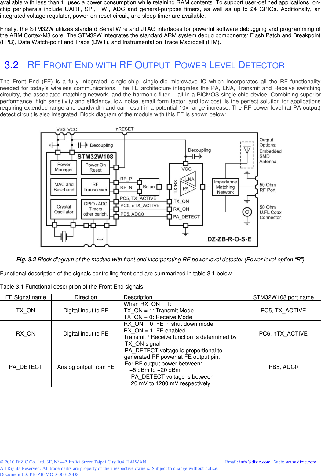
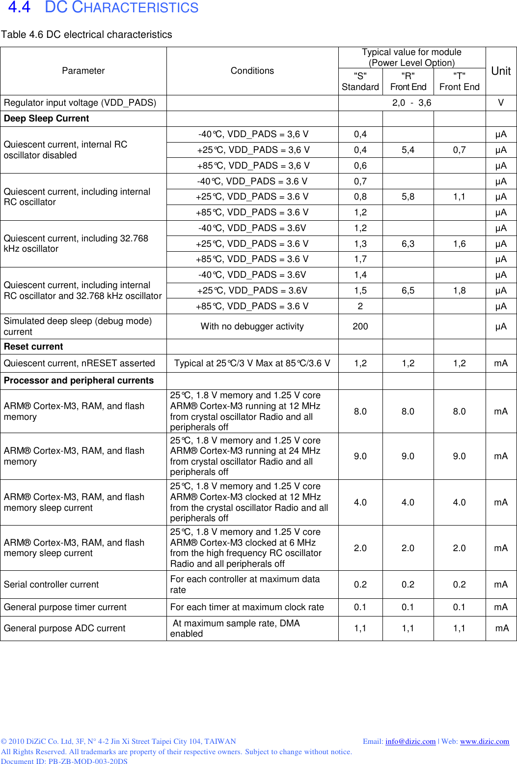
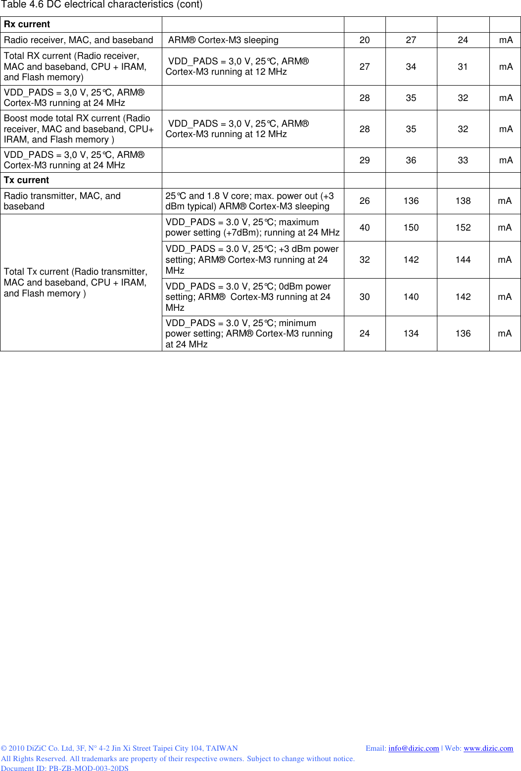
![© 2010 DiZiC Co. Ltd, 3F, N° 4-2 Jin Xi Street Taipei City 104, TAIWAN Email: info@dizic.com | Web: www.dizic.com All Rights Reserved. All trademarks are property of their respective owners. Subject to change without notice. Document ID: PB-ZB-MOD-003-20DS 4 ELECTRICAL CHARACTERISTICS 4.1 PARAMETER CONDITIONS Unless otherwise specified, all voltages are referenced to VSS. 4.1.1 Minimum and maximum values Unless otherwise specified the minimum and maximum values are guaranteed in the worst conditions of ambient temperature, supply voltage and frequencies by tests in production on 100% of the devices with an ambient temperature at TA = 25 °C and TA = TAmax (given by the selected temperature range). Data based on characterization results, design simulation and/or technology characteristics are indicated in the table footnotes and are not tested in production. Based on characterization, the minimum and maximum values refer to sample tests and represent the mean value plus or minus three times the standard deviation (mean ±3σ). 4.1.2 Typical values are given only as design guidelines and are not tested. Typical ADC accuracy values are determined by characterization of a batch of samples from a standard diffusion lot over the full temperature range. 4.2 ABSOLUTE MAXIMUM RATINGS Stresses above the absolute maximum ratings listed in Table 4.1: Voltage characteristics, Table 4.2: Current characteristics and Table 4.3: Thermal characteristics may cause permanent damage to the device. These are stress ratings only and functional operation of the device at these conditions is not implied. Exposure to maximum rating conditions for extended periods may affect device reliability. Table 4.1 Voltage characteristics Ratings Min. Max. Unit Regulator input voltage (VDD_PADS) -0.3 +3.6 V RF Input Power (for max level for correct packet reception Receive characteristics) RX signal into a lossless balun 15 dBm Voltage on any GPIO (PA[7:0], PB[7:0], PC[7:0]), SWCLK, nRESET, VREG_OUT -0.3 VDD_PADS +0.3 V Table 4.2 Current characteristics Symbol Ratings Max. Unit IVDD Total current into VDD/VDDA power lines (source) 150 mA IVSS Total current out of VSS ground lines (sink) 150 mA IIO Output current sunk by any I/O and control pin 25 mA Table 4.3 Thermal characteristics Symbol Ratings Value Unit TSTG Storage temperature range –40 to +140 °C TJ Maximum junction temperature 150 °C](https://usermanual.wiki/STMicroelectronicsS/DZSTM32WA.manual/User-Guide-1313171-Page-9.png)
![© 2010 DiZiC Co. Ltd, 3F, N° 4-2 Jin Xi Street Taipei City 104, TAIWAN Email: info@dizic.com | Web: www.dizic.com All Rights Reserved. All trademarks are property of their respective owners. Subject to change without notice. Document ID: PB-ZB-MOD-003-20DS 5.2 MODULE PAD DESCRIPTION The following table describes the pads of the module. Table 5.1: Pad Description Pad# Signal Direction Description 1 GND Power Ground supply pad 2 GND Power Ground supply pad 3 VCC Power Power supply pad 4 VCC Power Power supply pad 5 nRESET I Active low chip reset (internal pull-up) 6 PC5 I/O Digital I/O TX_ACTIVE O Logic-level control for external Rx/Tx switch. The STM32W108 baseband controls TX_ACTIVE and drives it high (VDD_PADS) when in Tx mode. Select alternate output function with GPIO_PCCFGH[7:4] 7 PC6 I/O Digital I/O OSC32B I/O 32.768 kHz crystal oscillator. Select analogue function with GPIO_PCCFGH[11 :8] nTX_ACTIVE O Inverted TX_ACTIVE signal (see PC5) Select alternate output function with GPIO_PCCFGH[11:8] 8 PC7 I/O Digital I/O OSC32A I/O 32.768 kHz crystal oscillator. Select analogue function with GPIO_PCCFGH[15:12] OSC32_EXT I Digital 32 kHz clock input source 9 PA7 I/O High current Digital I/O Disable REG_EN with GPIO_DBGCFG[4] TIM1CH4 O Timer 1 Channel 4 output Enable timer output with TIM1_CCER Select alternate output function with GPIO_PACFGH[15:12] Disable REG_EN with GPIO_DBGCFG[4] I Timer 1 Channel 4 input. Cannot be remapped REG_EN O External regulator open drain output. (Enabled after reset). 10 PB3 I/O Digital I/O TIM2_CH3 (see also Pad 13) O Timer 2 channel 3 output Enable remap with TIM2_OR[6] Enable timer output in TIM2_CCER Select alternate output function with GPIO_PBCFGL[15:12] I Timer 2 channel 3 input Enable remap with TIM2_OR[6] UART_CTS I UART CTS handshake of Serial Controller 1 Enable with SC1_UARTCFG[5] Select UART with SC1_MODE SC1SCLK O SPI master clock of Serial Controller 1 Either disable timer output in TIM2_CCER, or disable remap with TIM2_OR[6] Enable master with SC1_SPICFG[4] Select SPI with SC1_MODE Select alternate output function with GPIO_PBCFGL[15:12] I SPI slave clock of Serial Controller 1 Enable slave with SC1_SPICFG[4] Select SPI with SC1_MODE](https://usermanual.wiki/STMicroelectronicsS/DZSTM32WA.manual/User-Guide-1313171-Page-15.png)
![© 2010 DiZiC Co. Ltd, 3F, N° 4-2 Jin Xi Street Taipei City 104, TAIWAN Email: info@dizic.com | Web: www.dizic.com All Rights Reserved. All trademarks are property of their respective owners. Subject to change without notice. Document ID: PB-ZB-MOD-003-20DS Table 5.1: Pad Description (cont) Pad# Signal Direction Description 11 PB4 I/O Digital I/O TIM2_CH4 (see also Pad 15) O Timer 2 channel 4 output Enable remap with TIM2_OR[7] Enable timer output in TIM2_CCER Select alternate output function with GPIO_PBCFGH[3:0] I Timer 2 channel 4 input Enable remap with TIM2_OR[7] UART_RTS O UART RTS handshake of Serial Controller 1 Either disable timer output in TIM2_CCER, or disable remap with TIM2_OR[7] Enable with SC1_UARTCFG[5] Select UART with SC1_MODE Select alternate output function with GPIO_PBCFGH[3:0] SC1nSSEL I SPI slave select of Serial Controller 1 Enable slave with SC1_SPICFG[4] Select SPI with SC1_MODE 12 PA0 I/O Digital I/O TIM2_CH1 (see also Pad 20) O Timer 2 channel 1 output Disable remap with TIM2_OR[4] Enable timer output in TIM2_CCER Select alternate output function with GPIO_PACFGL[3:0] I Timer 2 channel 1 input Disable remap with TIM2_OR[4] SC2MOSI O SPI master data out of Serial Controller 2 Either disable timer output in TIM2_CCER, or enable remap with TIM2_OR[4] Enable master with SC2_SPICFG[4] Select SPI with SC2_MODE Select alternate output function with GPIO_PACFGL[3:0] I SPI slave data in of Serial Controller 2 Enable slave with SC2_SPICFG[4] Select SPI with SC2_MODE 13 PA1 I/O Digital I/O TIM2_CH3 (see also Pad 10) O Timer 2 channel 3 output Disable remap with TIM2_OR[6] Enable timer output in TIM2_CCER Select alternate output function with GPIO_PACFGL[7:4] I Timer 2 channel 3 input Disable remap with TIM2_OR[6] SC2SDA I/O TWI data of Serial Controller 2 Either disable timer output in TIM2_CCER, or enable remap with TIM2_OR[6] Select TWI with SC2_MODE Select alternate open-drain output function with GPIO_PACFGL[7:4] SC2MISO O SPI slave data out of Serial Controller 2 Either disable timer output in TIM2_CCER, or enable remap with TIM2_OR[6] Enable slave with SC2_SPICFG[4] Select SPI with SC2_MODE Select alternate output function with GPIO_PACFGL[7:4] I SPI master data in of Serial Controller 2 Enable slave with SC2_SPICFG[4] 14 GND Power Ground supply pad.](https://usermanual.wiki/STMicroelectronicsS/DZSTM32WA.manual/User-Guide-1313171-Page-16.png)
![© 2010 DiZiC Co. Ltd, 3F, N° 4-2 Jin Xi Street Taipei City 104, TAIWAN Email: info@dizic.com | Web: www.dizic.com All Rights Reserved. All trademarks are property of their respective owners. Subject to change without notice. Document ID: PB-ZB-MOD-003-20DS Table 5.1: Pad Description (cont) Pad# Signal Direction Description 15 PA2 I/O Digital I/O. TIM2_CH4 (see also Pad 11) O Timer 2 channel 4 output. Disable remap with TIM2_OR[7]. Enable timer output in TIM2_CCER . Select alternate output function with GPIO_PACFGL[11:8]. I Timer 2 channel 4 input Disable remap with TIM2_OR[7]. SC2SCL I/O TWI clock of Serial Controller 2. Either disable timer output in TIM2_CCER, or enable remap with TIM2_OR[7]. Select TWI with SC2_MODE. Select alternate open-drain output function with GPIO_PACFGL[11:8]. SC2SCLK O SPI master clock of Serial Controller 2. Either disable timer output in TIM2_CCER, or enable remap with TIM2_OR[7]. Enable master with SC2_SPICFG[4]. Select SPI with SC2_MODE. Select alternate output function with GPIO_PACFGL[11:8]. I SPI slave clock of Serial Controller 2. Enable slave with SC2_SPICFG[4]. Select SPI with SC2_MODE. 16 PA3 I/O Digital I/O SC2nSSEL I SPI slave select of Serial Controller 2 Enable slave with SC2_SPICFG[4] Select SPI with SC2_MODE TRACECLK (see also Pad 27) O Synchronous CPU trace clock . Either disable timer output in TIM2_CCER, or enable remap with TIM2_OR[5]. Enable trace interface in ARM core. Select alternate output function with GPIO_PACFGL[15:12]. TIM2_CH2 (see also Pad 21) O Timer 2 channel 2 output. Disable remap with TIM2_OR[5]. Enable timer output in TIM2_CCER. Select alternate output function with GPIO_PACFGL[15:12]. I Timer 2 channel 2 input Disable remap with TIM2_OR[5]. 17 PA4 I/O Digital I/O. ADC4 Analog ADC Input 4 Select analogue function with GPIO_PACFGH[3:0]. PTI_EN O Frame signal of Packet Trace Interface (PTI). Disable trace interface in ARM core. Select alternate output function with GPIO_PACFGH[3:0]. TRACEDATA2 O Synchronous CPU trace data bit 2. Select 4-wire synchronous trace interface in ARM core. Enable trace interface in ARM core. Select alternate output function with GPIO_PACFGH[3:0]. 18 PA5 I/O Digital I/O. ADC5 Analog ADC Inputs Select analog function with GPIO_PACFGH[7:4]. PTI_DATA O Data signal of Packet Trace Interface (PTI). Disable trace interface in ARM core. Select alternate output function with GPIO_PACFGH[7:4]. nBOOTMODE I Embedded serial boot-loader activation out of reset Signal is active during and immediately after a reset on nRESET. TRACEDATA3 O Synchronous CPU trace data bit 3. Select 4-wire synchronous trace interface in ARM core. Enable trace interface in ARM core. Select alternate output function with GPIO_PACFGH[7:4]. 19 PA6 I/O High current Digital I/O. TIM1_CH3 O Timer 1 channel 3 output. Enable timer output in TIM1_CCER. Select alternate output function with GPIO_PACFGH[11 :8]. I Timer 1 channel 3 input Cannot be remapped.](https://usermanual.wiki/STMicroelectronicsS/DZSTM32WA.manual/User-Guide-1313171-Page-17.png)
![© 2010 DiZiC Co. Ltd, 3F, N° 4-2 Jin Xi Street Taipei City 104, TAIWAN Email: info@dizic.com | Web: www.dizic.com All Rights Reserved. All trademarks are property of their respective owners. Subject to change without notice. Document ID: PB-ZB-MOD-003-20DS Table 5.1: Pad Description (cont) Pad# Signal Direction Description 20 PB1 I/O Digital I/O. SC1MISO O SPI slave data out of Serial Controller 1. Either disable timer output in TIM2_CCER, or disable remap with TIM2_OR[4]. Select SPI with SC1_MODE. Select slave with SC1_SPICR. Select alternate output function with GPIO_PBCFGL[7:4]. SC1MOSI O SPI master data out of Serial Controller 1. Either disable timer output in TIM2_CCER, or disable remap with TIM2_OR[4]. Select SPI with SC1_MODE. Select master with SC1_SPICR. Select alternate output function with GPIO_PBCFGL[7:4] SC1SDA I/O TWI data of Serial Controller 1. Either disable timer output in TIM2_CCER, or disable remap with TIM2_OR[4]. Select TWI with SC1_MODE. Select alternate open-drain output function with GPIO_PBCFGL[7:4]. SC1TXD O UART transmit data of Serial Controller 1. Either disable timer output in TIM2_CCER, or disable remap with TIM2_OR[4]. Select UART with SC1_MODE. Select alternate output function with GPIO_PBCFGL[7:4]. TIM2_CH1 (see also Pad 12) O Timer 2 channel 1 output. Enable remap with TIM2_OR[4]. Enable timer output in TIM2_CCER. Select alternate output function with GPIO_PACFGL[7:4]. I Timer 2 channel 1 input Disable remap with TIM2_OR[4]. 21 PB2 I/O Digital I/O SC1MISO I SPI master data in of Serial Controller 1. Select SPI with SC1_MODE. Select master with SC1_SPICR. SC1MOSI I SPI slave data in of Serial Controller 1. Select SPI with SC1_MODE. Select slave with SC1_SPICR SC1SCL I/O TWI clock of Serial Controller 1. Either disable timer output in TIM2_CCER, or disable remap with TIM2_OR[5]. Select TWI with SC1_MODE. Select alternate open-drain output function with GPIO_PBCFGL[11 :8]. SC1RXD I UART receive data of Serial Controller 1. Select UART with SC1_MODE. TIM2_CH2 (see also Pad 16) O Timer 2 channel 2 output. Enable remap with TIM2_OR[5]. Enable timer output in TIM2_CCER. Select alternate output function with GPIO_PBCFGL[11 :8]. I Timer 2 channel 2 input. Enable remap with TIM2_OR[5]. 22 SWCLK I/O Serial Wire clock input/output with debugger. Selected when in Serial Wire mode (see JTMS description, Pad 26) JTCK 1 JTAG clock input from debugger. Selected when in JTAG mode (default mode, see JTMS description, Pad 26) Internal pull-down is enabled. 23 PC2 I/O Digital I/O. Enable with GPIO_DBGCFG[5]. JTDO O JTAG data out to debugger. Selected when in JTAG mode (default mode, see JTMS description, Pad 26). SWO O Serial Wire Output asynchronous trace output to debugger. Select asynchronous trace interface in ARM core. Enable trace interface in ARM core. Select alternate output function with GPIO_PCCFGL[11:8]. Enable Serial Wire mode (see JTMS description, Pad 26). Internal pull-up is enabled.](https://usermanual.wiki/STMicroelectronicsS/DZSTM32WA.manual/User-Guide-1313171-Page-18.png)
![© 2010 DiZiC Co. Ltd, 3F, N° 4-2 Jin Xi Street Taipei City 104, TAIWAN Email: info@dizic.com | Web: www.dizic.com All Rights Reserved. All trademarks are property of their respective owners. Subject to change without notice. Document ID: PB-ZB-MOD-003-20DS Table 5.1: Pad Description (cont) Pad# Signal Direction Description 24 PC3 I/O Digital I/O Either Enable with GPIO_DBGCFG[5], or enable Serial Wire mode (see JTMS description, Pad 26) JTDI 1 JTAG data in from debugger Selected when in JTAG mode (default mode, see JTMS description, Pad 26). Internal pull-up is enabled. 25 GND Power Ground supply pad. 26 PC4 I/O Digital I/O Enable with GPIO_DBGCFG[5] JTMS I JTAG mode select from debugger. Selected when in JTAG mode (default mode). JTAG mode is enabled after power-up or by forcing nRESET low. Select Serial Wire mode using the ARM-defined protocol through a debugger. Internal pull-up is enabled. SWDIO I/O Serial Wire bidirectional data to/from debugger. Enable Serial Wire mode (see JTMS description). Select Serial Wire mode using the ARM-defined protocol through a debugger. Internal pull-up is enabled. 27 PB0 I/O Digital I/O VREF Analog O ADC reference output. Enable analog function with GPIO_PBCFGL[3:0] VREF Analog I ADC reference input. Enable analog function with GPIO_PBCFGL[3:0]. Enable reference output with an STM system function IRQA I External interrupt source A. TRACECLK (see also Pad 16) O Synchronous CPU trace clock. Enable trace interface in ARM core. Select alternate output function with GPIO_PBCFGL[3:0]. TIM1CLK I Timer 1 external clock input TIM2MSK I Timer 2 external clock mask input 28 GND Power Ground supply pad. 29 PC1 I/O Digital I/O ADC3 Analog ADC Inputs Enable analog function with GPIO_PCCFGL[7:4] SWO (see also Pad 23) O Serial Wire Output asynchronous trace output to debugger. Select asynchronous trace interface in ARM core. Enable trace interface in ARM core. Select alternate output function with GPIO_PCCFGL[7:4]. TRACEDATA0 O Synchronous CPU trace data bit 0. Select 1-, 2- or 4-wire synchronous trace interface in ARM core. Enable trace interface in ARM core. Select alternate output function with GPIO_PCCFGL[7:4]. 30 PC0 I/O High current Digital I/O. Either enable with GPIO_DBGCFG[5], or enable Serial Wire mode (see JTMS description, Pad 26) and disable TRACEDATA1. JRST I JTAG reset input from debugger. Selected when in JTAG mode (default mode, see JTMS description) and TRACEDATA1 is disabled. Internal pull-up is enabled. IRQD1 I Default external interrupt source D TRACEDATA1 O Synchronous CPU trace data bit 1. Select 2- or 4-wire synchronous trace interface in ARM core. Enable trace interface in ARM core. Select alternate output function with GPIO_PCCFGL[3:0].](https://usermanual.wiki/STMicroelectronicsS/DZSTM32WA.manual/User-Guide-1313171-Page-19.png)
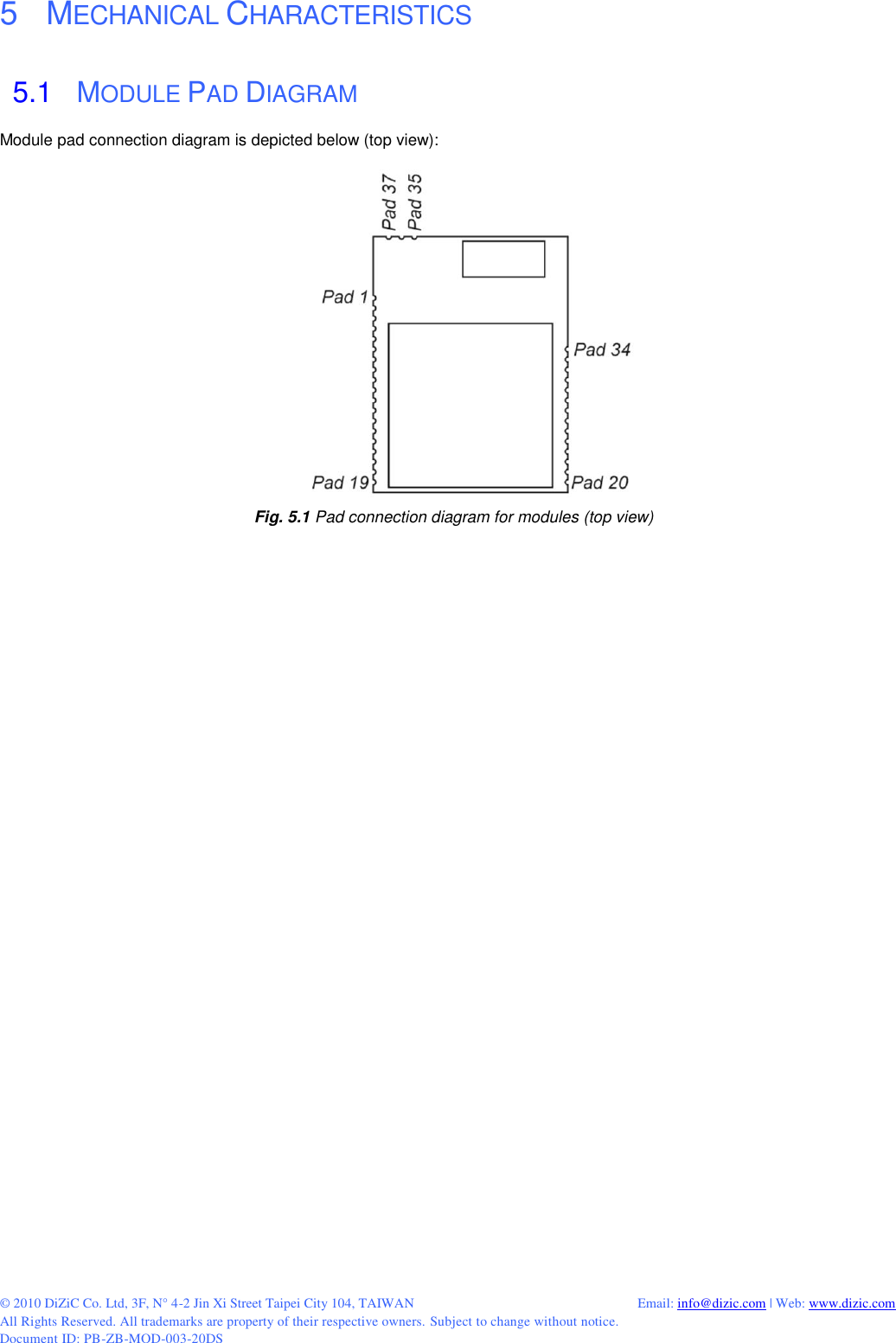
![© 2010 DiZiC Co. Ltd, 3F, N° 4-2 Jin Xi Street Taipei City 104, TAIWAN Email: info@dizic.com | Web: www.dizic.com All Rights Reserved. All trademarks are property of their respective owners. Subject to change without notice. Document ID: PB-ZB-MOD-003-20DS Table 5.1: Pad Description (cont) Pad# Signal Direction Description 31 PB7 I/O High current Digital I/O ADC2 Analog ADC Input 2 Enable analog function with GPIO_PBCFGH[15:12] IRQC1 I Default external interrupt source C TIM1_CH2 O Timer 1 channel 2 output. Enable timer output in TIM1_CCER. Select alternate output function with GPIO_PBCFGH[15:12]. I Timer 1 channel 2 input .(Cannot be remapped). 32 PB6 I/O High current Digital I/O. ADC1 Analog ADC Input 1. Enable analog function with GPIO_PBCFGH[11:8]. IRQB I External interrupt source B. TIM1_CH1 O Timer 1 channel 1 output. Enable timer output in TIM1_CCER. Select alternate output function with GPIO_PBCFGH[11:8]. I Timer 1 channel 1 input. (Cannot be remapped). 33 PB5 I/O Digital I/O ADC0 Analog ADC Input 0. Enable analog function with GPIO_PBCFGH[7:4]. TIM2CLK I Timer 2 external clock input. TIM1MSK I Timer 2 external clock mask input. 34 GND Power Ground supply pad. 35 GNDRF RF Ground Ground pad for RF port. 36 RF Analog RF port with 50 Ohm impedance. 37 GNDRF RF Ground Ground pad for RF port. 5.3 PACKAGE MECHANICAL DIMENSIONS Module dimensions are 25 mm x 19 mm x 2 mm and detailed drawing is shown below on Fig. 5.2. Fig. 5.2 Dimensions of the module. Left: EMI Option “S” -- without shielding; Right: Option “M” – with metal shielding (Enhanced EMI protection)](https://usermanual.wiki/STMicroelectronicsS/DZSTM32WA.manual/User-Guide-1313171-Page-20.png)
![© 2010 DiZiC Co. Ltd, 3F, N° 4-2 Jin Xi Street Taipei City 104, TAIWAN Email: info@dizic.com | Web: www.dizic.com All Rights Reserved. All trademarks are property of their respective owners. Subject to change without notice. Document ID: PB-ZB-MOD-003-20DS 9 REFERENCES & REVISION HISTORY [1]. STM32W108HB, STM32W108CB, High-performance, 802.15.4 wireless system-on-chip, Data brief, 20-Aug-2009, Rev. 1 [2]. STM32W108HB, STM32W108CB, High-performance, 802.15.4 wireless system-on-chip, Preliminary data, 01-Mar-2010, Rev. 4 [3]. RN0034, Release notes, STM32W108xx starter and extension kits EmberZNet 4.0.2 GA, Doc ID 16225, 16-Feb-2010, Rev. 2 [4]. RN0047, Release notes, STM32W108xx starter and extension kits ZigBee RF4CE, Doc ID 17098, 23-Feb-2010, Rev. 1 [5]. RN0046, Release note, STM32W108xx starter and extension kits for Simple MAC library, Doc ID 16996, 04-March-2010, Rev. 1 [6]. UM0894, User Manual, STM32W-SK and STM32W-EXT starter and extension kits for STM32W108xx, Doc ID 16999, 05-Feb-2010, Rev. 1 [7]. UM0847, User Manual, IAR customization for STM32W108 system-on-chip, Doc ID 16551, 16-Nov-2009, Rev. 1.](https://usermanual.wiki/STMicroelectronicsS/DZSTM32WA.manual/User-Guide-1313171-Page-25.png)