STMicroelectronicsS DZSTM32WA DZ-SB-S-A Zigbee Module User Manual DiZiC ZigBee Modules
STMicroelectronics DZ-SB-S-A Zigbee Module DiZiC ZigBee Modules
Contents
- 1. manual
- 2. chip antenna datasheet
manual
© 2010 DiZiC Co. Ltd, 3F, N° 4-2 Jin Xi Street Taipei City 104, TAIWAN Email: info@dizic.com | Web: www.dizic.com
All Rights Reserved. All trademarks are property of their respective owners. Subject to change without notice.
Document ID: PB-ZB-MOD-003-20DS
802.15.4 Family of RF Modules
High Performance and Long Range
802.15.4 STM32W RF Modules
Quickly add wireless capability with these high performance ZigBee compliant modules
READY TO USE SoC RF MODULES
Quickly add wireless networking capabilities to your
products with these ready-to-use DiZiC 802.15.4 RF
Modules. Simple to operate and available in a wide range of
configurations, these ZigBee compliant RF modules are
ideal for industrial sensors, consumer remote controls,
home appliances, and more.
Based on the STM32W108 wireless System-on-Chip
(SoC) from STMicroelectronics, this family of modules offer
outstanding RF performance with a -99 dBm normal RX
sensitivity (configurable to -100 dBm) and +3 dBm
normal mode output power (configurable up to +7 dBm).
With a small form factor and pin-to-pin compatible, DiZiC
802.15.4 RF Modules are available with several software
stack options, including EmberZNet PRO, RF4CE stack, or
proprietary low level MAC / PHY stack.
VERSATILE CONFIGURATIONS
With several possible configurations, select from 3 power
level options, 3 output options, 3 software stack options
and 2 EMI options:
Power Level Options - Choose from a standard power
level (+7 dBm), and two versions of RF front end (PA and
LNA, +20 dBm).
RF Output Options - Choose from a chip antenna, a U.FL
connector, or a single port 50 Ohm RF pad.
The U.FL connector allows, amongst other uses, for
connecting an external antenna, for connecting to an
application board that provides additional filters, or for
connecting to another 50 Ohm coaxial cable TX line. The
single port 50 Ohm RF pad allows for a direct connection
to another board, application module, or external antenna.
Software Stack Options - Choose from EmberZNet
PRO, RF4CE, or a low level PHY / MAC stack.
EmberZNet PRO is an easy to use ZigBee platform for
complex mesh networks. RF4CE (Radio Frequency for
Consumer Electronics) is a new protocol for consumer
remote controlled equipment. Custom applications can be
developed on top of a simple to use and low footprint
PHY/MAC API library.
EMI Options – Choose metal shielding protection where
enhanced electromagnetic interference immunity is
required otherwise standard version without metal
shielding is advisable.
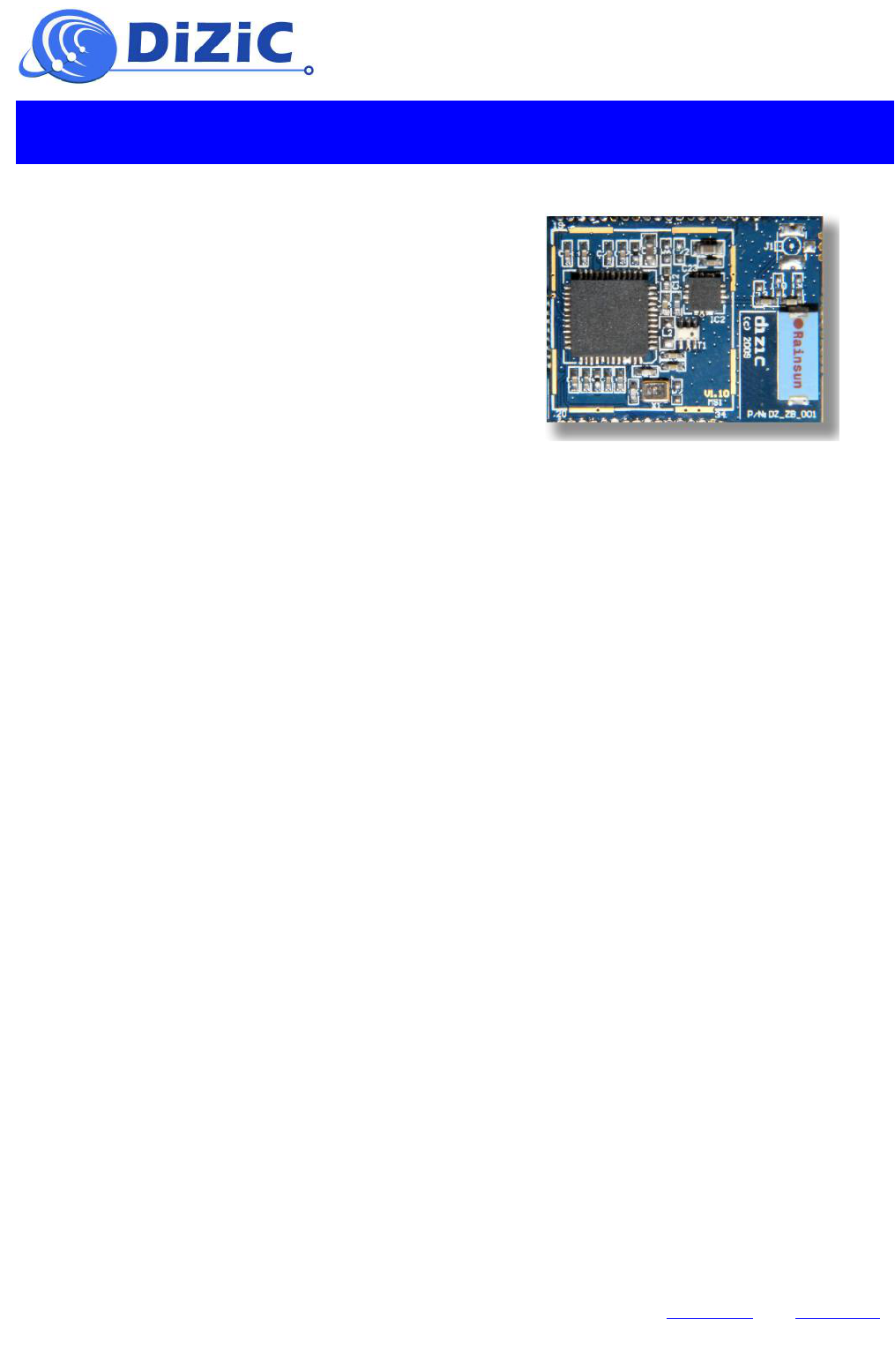
D/Z/C 802.15.4 STM32WRF Module with
RF front end and antenna
Key Features
• STM32W108 ZigBee / IEEE 802.15.4 SoC
• 32-bit ARM Cortex-M3 processor
• 128 kB of Flash and 8 kB of SRAM
• JTAG / SWD (programming and debugging)
• 2.4 GHz ISM supporting 16 channels
• Data rate up to 250 kbit/s
• 128-bit AES encryption
• Peripherals
• 24 GPIOs, SPI, USART, and I2C
• 12-bit ADC with up to 6 inputs
• 2x 16-bit timers
• DMA controller
• Standard module
• RX Sensitivity -99 dBm (-100 dBm Boost)
• TX Power 3 dBm (+7 dBm Boost)
• RF front end options
• Two Front End options
• Both with RX Sensitivity -105 dBm
• Both with TX Power +20 dBm
• RF Options
• Chip antenna, U.FL connector, or single port 50 Ohm
RF pad
• Shielding option for enhanced EMI protection
Ordering Information
DZ_ZB_[P] [O] [S][E] , where:
[P] Power level options, one of: S (standard +7 dBm), R (Front End
with Power Level Detect +20 dBm), or T (Front End +20 dBm)
[O] Output options, one of: A (Embedded SMD antenna assembled on
module), P (Single ended 50 Ohm. RF Pad), or U (50 Ohm U.FL
coaxial connector)
[S] Stack options, one of: F (RF4CE stack), X (Proprietary stack), or
Z (EmberZNet PRO stack)
[E] EMI protection options, one of: S (standard, no shielding), or
M (enhanced, with metal shield)

© 2010 DiZiC Co. Ltd, 3F, N° 4-2 Jin Xi Street Taipei City 104, TAIWAN Email: info@dizic.com | Web: www.dizic.com
All Rights Reserved. All trademarks are property of their respective owners. Subject to change without notice.
Document ID: PB-ZB-MOD-003-20DS
TABLE OF CONTENT
1 FEATURE LIST....................................................................................................................................... 3
2 MODULE VARIANTS............................................................................................................................... 4
2.1 INTRODUCTION ............................................................................................................................ 4
2.2 DIZIC 802.15.4 RF MODULE: OUTPUT OPTIONS ...................................................................... 4
2.3 DIZIC 802.15.4 RF MODULE: POWER LEVEL OPTIONS ............................................................ 5
2.4 DIZIC 802.15.4 RF MODULE: STACK OPTIONS ........................................................................ 5
2.5 DIZIC 802.15.4 RF MODULE: EMI PROTECTION OPTIONS ...................................................... 5
3 COMPONENTS OVERVIEW .................................................................................................................... 6
3.1 STM32W108 – SYSTEM-ON-CHIP ............................................................................................ 6
3.2 RF FRONT END WITH RF OUTPUT POWER LEVEL DETECTOR ................................................. 7
3.3 RF FRONT END ........................................................................................................................... 8
3.4 ZIGBEE STACKS .......................................................................................................................... 8
4 ELECTRICAL CHARACTERISTICS ........................................................................................................... 9
4.1 PARAMETER CONDITIONS ........................................................................................................... 9
4.1.1 Minimum and maximum values ............................................................................................ 9
4.1.2 Typical values .......................................................................................................................... 9
4.2 ABSOLUTE MAXIMUM RATINGS .................................................................................................... 9
4.3 OPERATING CONDITIONS .......................................................................................................... 10
4.3.1 General operating conditions .............................................................................................. 10
4.3.2 Electrostatic discharge (ESD) ............................................................................................. 10
4.4 DC CHARACTERISTICS ............................................................................................................. 11
4.5 RF CHARACTERISTIC ................................................................................................................ 13
4.5.1 Receiver ................................................................................................................................. 13
4.5.2 Transmitter ............................................................................................................................. 13
5 MECHANICAL CHARACTERISTICS ........................................................................................................ 14
5.1 MODULE PAD DIAGRAM ............................................................................................................ 14
5.2 MODULE PAD DESCRIPTION ..................................................................................................... 15
5.3 PACKAGE MECHANICAL DIMENSIONS ....................................................................................... 20
6 SOLDERING ........................................................................................................................................ 21
6.1 SOLDER TEMPERATURE PROFILE ........................................................................................... 21
6.2 PROFILE PARAMETERS ............................................................................................................ 21
6.3 RECOMMENDED FOOTPRINT .................................................................................................... 22
7 ORDERING INFORMATION ................................................................................................................... 23
8 LIST OF ACRONYMS ............................................................................................................................ 24
9 REFERENCES & REVISION HISTORY ................................................................................................... 25
© 2010 DiZiC Co. Ltd, 3F, N° 4-2 Jin Xi Street Taipei City 104, TAIWAN Email: info@dizic.com | Web: www.dizic.com
All Rights Reserved. All trademarks are property of their respective owners. Subject to change without notice.
Document ID: PB-ZB-MOD-003-20DS
DIZIC 802.15.4 RF MODULE DZ-ZB-[P]-[O]-[S]-[E] DATA SHEET
POWER LEVEL OPTIONS
STANDARD FRONT END FRONT END WITH
RF POWER LEVEL DETECTOR
1 FEATURE LIST
Complete System-on-Chip
• 32-bit ARM® Cortex-M3 processor
• 2.4 GHz IEEE 802.15.4 transceiver & lower MAC
• 128 kB flash, 8kB RAM memory
• AES128 encryption accelerator
• Flexible ADC, SPI/UART/TWI serial communications, and
general purpose timers
• 24 highly configurable GPIO with Schmitt trigger inputs
Industry-leading ARM Cortex-M3 processor
• Leading 32-bit processing performance
• Highly efficient Thumb-2 instruction set
• Operation at 6, 12 or 24 MHz
• Flexible Nested Vectored Interrupt Controller
Low power consumption, advanced management
• RX Current (w/ CPU): 27 mA
• TX Current (w/ CPU, +3 dBm TX): 31 mA
• Low deep sleep current, with retained RAM and GPIO:
400 nA/800 nA with/without sleep timer
• Low-frequency internal RC oscillator for low-power sleep
timing
• High-frequency internal RC oscillator for fast (100 µsec)
processor start-up from sleep
Innovative network and processor debug
• Serial Wire/JTAG interface
• Standard ARM debug capabilities: Flash Patch &
Breakpoint; Data Watch-point & Trace; Instrumentation
Trace Macrocell
Exceptional RF Performance
• Normal mode Link Budget up to 102 dB; configurable up
to107dB
• -99 dBm normal RX sensitivity; configurable to -100 dBm
(1%PER, 20 byte packet)
• +3 dB normal mode output power; configurable up to +7
dBm
• Robust WiFi and Bluetooth coexistence
Application Flexibility
• Single voltage operation: 2.1-3.6 V
• Optional 32.768 kHz crystal for higher timer accuracy
• Low external component count with single 24 MHz crystal
• External power amplifier versions
Target applications for the Modules
include:
• Smart Energy
• Building automation and control (HVAC)
• Home automation and control
• Security and monitoring
• AMR/AMI
• Logistic & Asset tracking
• Medical
• General ZigBee wireless sensor networking
• Active RFID
• Wireless handheld terminals
• Industry telemetry and automatic data collection system
• Temperature and humidity control system
• Traffic and control for street lamp
© 2010 DiZiC Co. Ltd, 3F, N° 4-2 Jin Xi Street Taipei City 104, TAIWAN Email: info@dizic.com | Web: www.dizic.com
All Rights Reserved. All trademarks are property of their respective owners. Subject to change without notice.
Document ID: PB-ZB-MOD-003-20DS
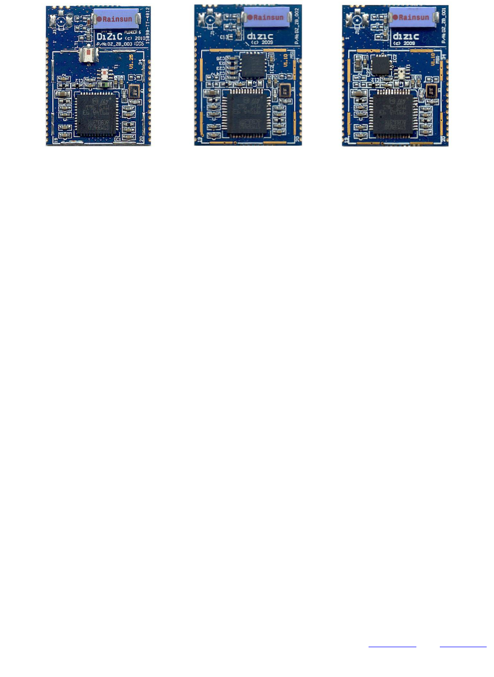
2 MODULE VARIANTS
2.1 INTRODUCTION
The DZ-ZB is low-power, high sensitivity IEEE 802.15.4 / ZigBee-compliant module. This multi-functional device based on
STMicroelectronics STM32W108 fully integrated System-on-Chip [1]. The STM32W108 integrates a 2.4 GHz, IEEE 802.15.4-
compliant transceiver, 32-bit ARM® Cortex™-M3 microprocessor, Flash and RAM memory, and peripherals of use to
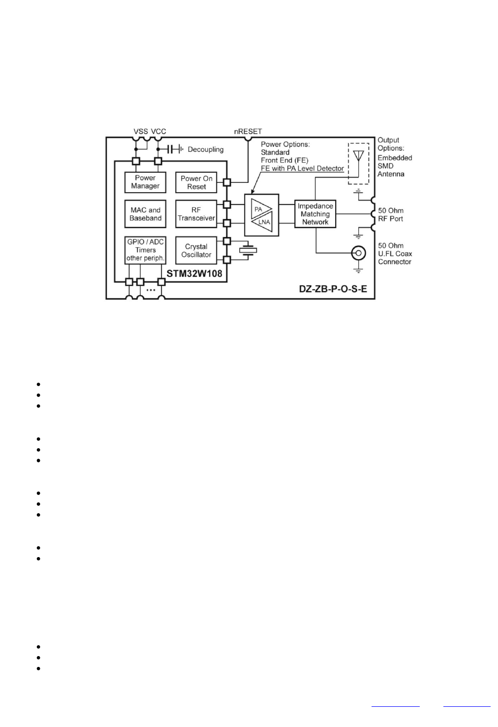
designers of ZigBee-based systems [2]. Block diagrams of DZ-ZB Module is show on Figure 2.1 and utilizes
STM32W108CBU6x version of the high performance, IEEE 802.15.4 compliant, wireless system-on-chip STM32W108 family.
Fig. 2.1 Block diagram of DZ-ZB Modules
DZ-ZB modules are available in two different product lines: without/with PA/LNA Front-End (FE). Both product lines
offering three ZigBee stack configurations. The first decision you need to make is if you want the Output option. The
following options are available:
A - Embedded SMD Antenna
P - Single ended 50 Ohm RF Pad
U - U.FL 50 Ohm coaxial connector
The second decision you need to make is Power level option. The following options are available:
S - Standard + 7dBm
R - Front End (PA and LNA) with RF output power level detector + 20 dBm
T - Front End (PA and LNA) + 20 dBm
The third decision you need to make ZigBee stack. The following options are available:
F - RF4CE stack
X - Proprietary stack
Z - EmberZnet PRO stack
The final decision is level of electromagnetic immunity (EMI) protection. The following options are available:
M - Metal cap shielding enabling enhanced level of electromagnetic immunity (EMI) protection
S - Standard, without metal shielding cap
The next chapters will explain each of all options.
2.2 DIZIC 802.15.4 RF MODULE: OUTPUT OPTIONS
The following Output Options are available:
A - Embedded SMD Antenna
P - Single ended 50 Ohm RF Pad
U - U.FL 50 Ohm coaxial connector

© 2010 DiZiC Co. Ltd, 3F, N° 4-2 Jin Xi Street Taipei City 104, TAIWAN Email: info@dizic.com | Web: www.dizic.com
All Rights Reserved. All trademarks are property of their respective owners. Subject to change without notice.
Document ID: PB-ZB-MOD-003-20DS
2.3 DIZIC 802.15.4 RF MODULE: POWER LEVEL OPTIONS
The following Power Level Options are available:
Option S - Standard + 7dBm
STM32W chip: System on Chip - where radio, microcontroller, program/user memory, RAM, ZigBee protocols stack are
integrated in one chip.
Option R - Front End (PA and LNA) with RF output power level detector + 20 dBm
STM32W chip: System on Chip - where radio, microcontroller, program/user memory, RAM, ZigBee protocols stack are
integrated in one chip.
Option T - Front End (PA and LNA) + 20 dBm
STM32W chip: System on Chip - where radio, microcontroller, program/user memory, RAM, ZigBee protocols stack are
integrated in one chip.
2.4 DIZIC 802.15.4 RF MODULE: STACK OPTIONS
The following ZigBee stack options are available:
Option F - RF4CE stack
Option X - Proprietary stack
Option Z - EmberZnet PRO stack
Instructions concerning to programming ST32W108 you will find at [7] and examples of Application at [6].
2.5 DIZIC 802.15.4 RF MODULE: EMI PROTECTION OPTIONS
The following EMI protection options are available:
Option M - Metal shield cap enabling enhanced level of electromagnetic immunity (EMI) protection
Option S - Standard module without metal shielding
© 2010 DiZiC Co. Ltd, 3F, N° 4-2 Jin Xi Street Taipei City 104, TAIWAN Email: info@dizic.com | Web: www.dizic.com
All Rights Reserved. All trademarks are property of their respective owners. Subject to change without notice.
Document ID: PB-ZB-MOD-003-20DS
3 COMPONENTS OVERVIEW
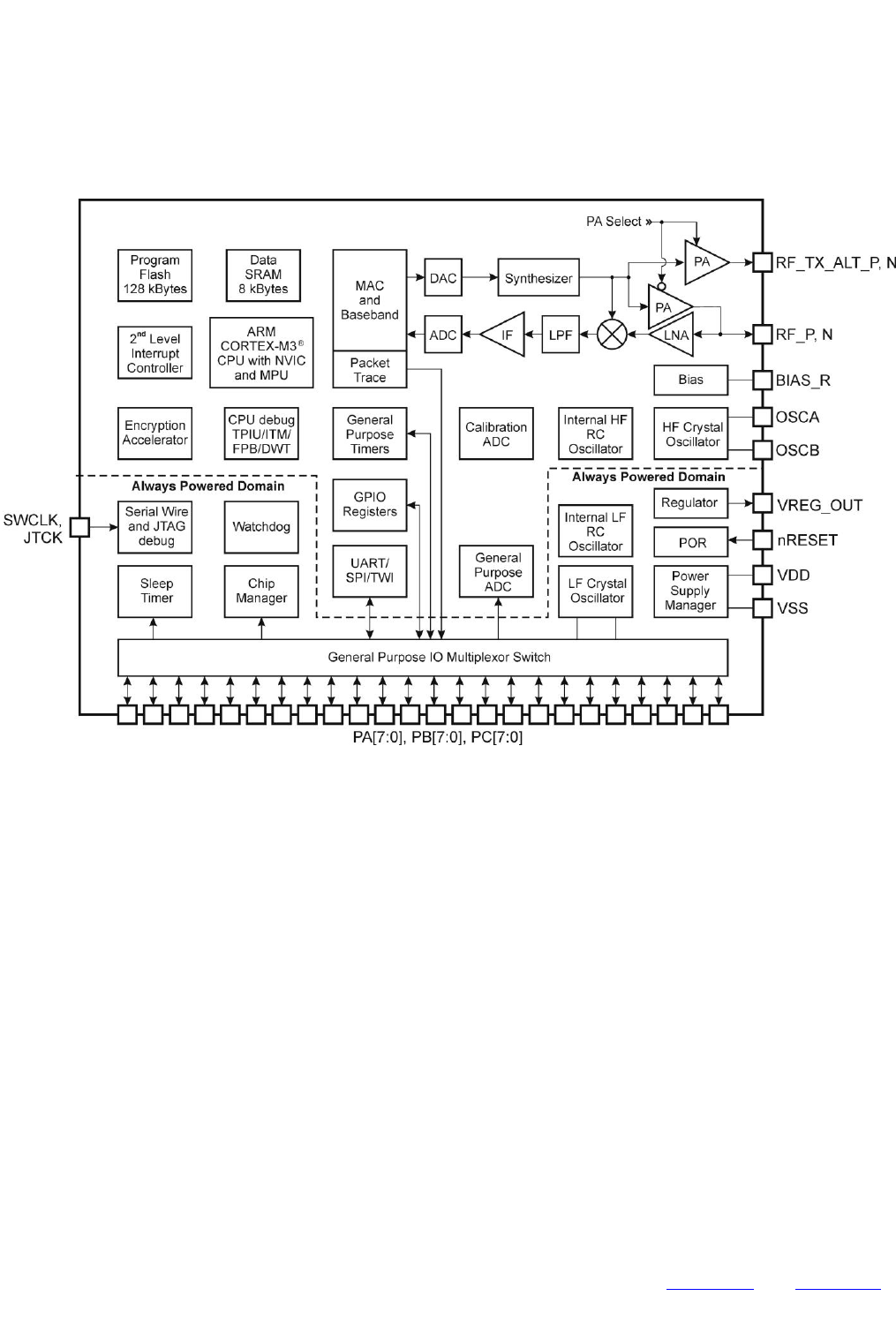
3.1 STM32W108 – SYSTEM-ON-CHIP
The is a fully The is a fully integrated System-on-Chip that integrates a 2.4 GHz, IEEE 802.15.4-compliant transceiver, 32-bit
ARM® Cortex™-M3 microprocessor, Flash and RAM memory, and peripherals of use to designers of ZigBee-based systems.
Block diagram of STM32W108 is show on Fig. 3.1 below:
Fig. 3.1 Block diagram of System-on-Chip STM32W108
The transceiver utilizes an efficient architecture that exceeds the dynamic range requirements imposed by the IEEE 802.15.4-
2003 standard by over 15 dB. The integrated receive channel filtering allows for robust co-existence with other communication
standards in the 2.4 GHz spectrum, such as IEEE 802.11 and Bluetooth. The integrated regulator, VCO, loop filter, and power
amplifier keep the external component count low. An optional high performance radio mode (boost mode) is software-
selectable to boost dynamic range.
The integrated 32-bit ARM® Cortex™-M3 microprocessor is highly optimized for high performance, low power consumption,
and efficient memory utilization. Including an integrated MPU, it supports two different modes of operation: System mode and
Application mode. The networking stack software runs in System mode with full access to all areas of the chip. Application
code runs in Application mode with limited access to the STM32W108 resources; this allows for the scheduling of events by
the application developer while preventing modification of restricted areas of memory and registers. This architecture results in
increased stability and reliability of deployed solutions.
The STM32W108 has 128 Kbytes of embedded Flash memory and 8 Kbytes of integrated RAM for data and program storage.
The STM32W108 HAL software employs an effective wear-levelling algorithm that optimizes the lifetime of the embedded
Flash.
To maintain the strict timing requirements imposed by the ZigBee and IEEE 802.15.4-2003 standards, the STM32W108
integrates a number of MAC functions into the hardware. The MAC hardware handles automatic ACK transmission and
reception, automatic back off delay, and clear channel assessment for transmission, as well as automatic filtering of received
packets. A packet trace interface is also integrated with the MAC, allowing complete, non-intrusive capture of all packets to
and from the STM32W108.
The STM32W108 offers a number of advanced power management features that enable long battery life. A high-frequency
internal RC oscillator allows the processor core to begin code execution quickly upon waking. Various deep sleep modes are
© 2010 DiZiC Co. Ltd, 3F, N° 4-2 Jin Xi Street Taipei City 104, TAIWAN Email: info@dizic.com | Web: www.dizic.com
All Rights Reserved. All trademarks are property of their respective owners. Subject to change without notice.
Document ID: PB-ZB-MOD-003-20DS
available with less than 1 μsec a power consumption while retaining RAM contents. To support user-defined applications, on-
chip peripherals include UART, SPI, TWI, ADC and general-purpose timers, as well as up to 24 GPIOs. Additionally, an
integrated voltage regulator, power-on-reset circuit, and sleep timer are available.
Finally, the STM32W utilizes standard Serial Wire and JTAG interfaces for powerful software debugging and programming of
the ARM Cortex-M3 core. The STM32W integrates the standard ARM system debug components: Flash Patch and Breakpoint
(FPB), Data Watch-point and Trace (DWT), and Instrumentation Trace Macrocell (ITM).
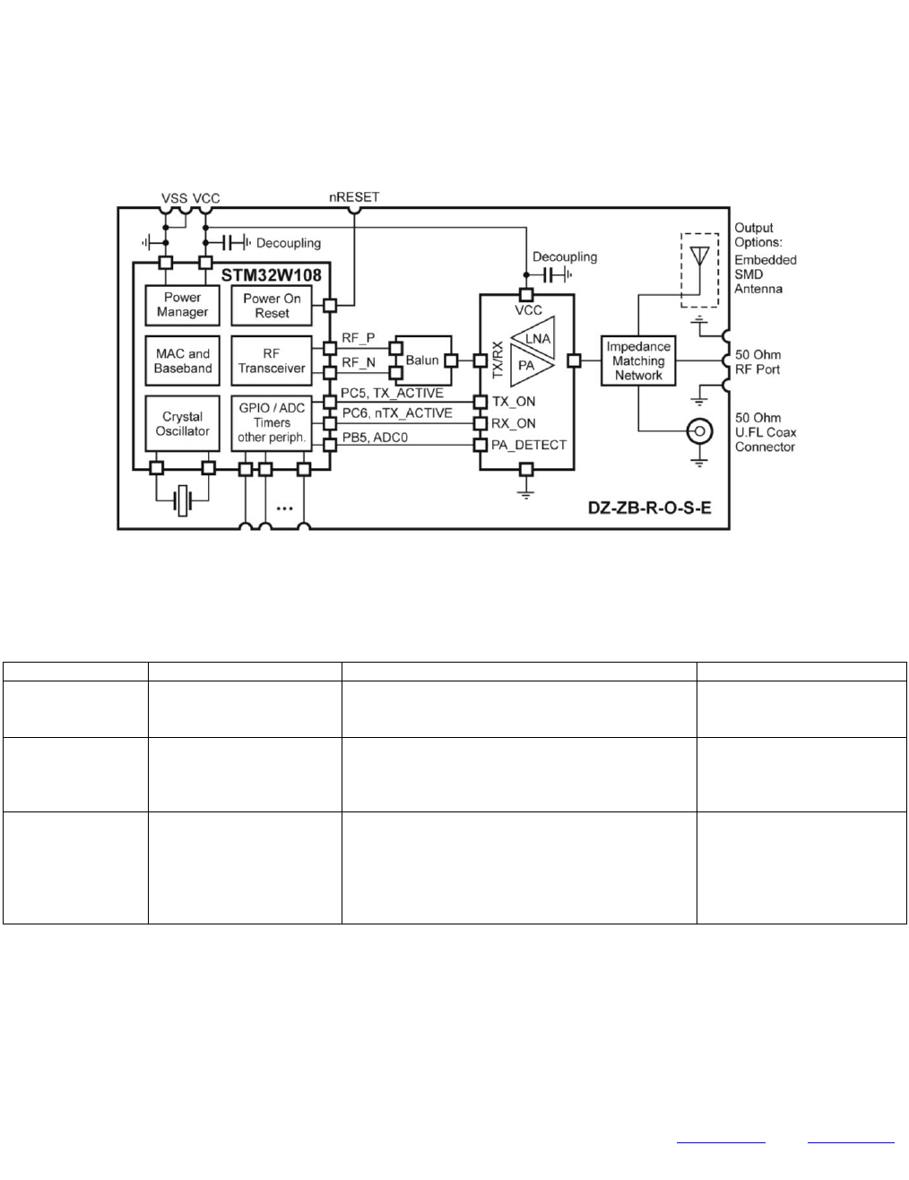
3.2 RF FRONT END WITH RF OUTPUT POWER LEVEL DETECTOR
The Front End (FE) is a fully integrated, single-chip, single-die microwave IC which incorporates all the RF functionality
needed for today’s wireless communications. The FE architecture integrates the PA, LNA, Transmit and Receive switching
circuitry, the associated matching network, and the harmonic filter -- all in a BiCMOS single-chip device. Combining superior
performance, high sensitivity and efficiency, low noise, small form factor, and low cost, is the perfect solution for applications
requiring extended range and bandwidth and can result in a potential 10x range increase. The RF power level (at PA output)
detect circuit is also integrated. Block diagram of the module with this FE is shown below:
Fig. 3.2 Block diagram of the module with front end incorporating RF power level detector (Power level option “R”)
Functional description of the signals controlling front end are summarized in table 3.1 below
Table 3.1 Functional description of the Front End signals
FE Signal name
Direction
Description
STM32W108 port name
TX_ON
Digital input to FE
When RX_ON = 1:
TX_ON = 1: Transmit Mode
TX_ON = 0: Receive Mode
PC5, TX_ACTIVE
RX_ON
Digital input to FE
RX_ON = 0: FE in shut down mode
RX_ON = 1: FE enabled
Transmit / Receive function is determined by
TX_ON signal
PC6, nTX_ACTIVE
PA_DETECT
Analog output from FE
PA_DETECT voltage is proportional to
generated RF power at FE output pin.
For RF output power between:
+5 dBm to +20 dBm
PA_DETECT voltage is between
20 mV to 1200 mV respectively
PB5, ADC0
© 2010 DiZiC Co. Ltd, 3F, N° 4-2 Jin Xi Street Taipei City 104, TAIWAN Email: info@dizic.com | Web: www.dizic.com
All Rights Reserved. All trademarks are property of their respective owners. Subject to change without notice.
Document ID: PB-ZB-MOD-003-20DS
3.3 RF FRONT END
This is a cost-effective and high performance RF Front End for low-power and low-voltage 2.4-GHz wireless applications. It is
a range extender for all existing and future 2.4-GHz low-power RF transceivers, transmitters and System-on-Chip products. It
increases the link budget by providing a power amplifier for increased output power, and an LNA with low noise figure for
improved receiver sensitivity. This FE consists of PA, LNA, RF switches, RF impedance matching, and balun for high
performance wireless applications. Module Block diagram with this Front End is shown below:
Fig. 3.3 Block diagram of the module with front end (Power level option “T”)
Functional description of the signals controlling front end are summarized in table 3.2 below
Table 3.2 Functional description of the Front End signals
FE Signal name
Direction
Description
STM32W108 port name
TxRx
Digital input to FE
When ENABLE = 1:
TxRx = 1: Transmit Mode
TxRx = 0: Receive Mode
PC5, TX_ACTIVE
HIGH_GAIN
Digital input to FE
Receive only (ENABLE = 1, TxRx = 0):
HIGH_GAIN = 1: LNA is in High Gain Mode.
LNA Gain = approx. 11dB
HIGH_GAIN = 0: LNA is in Lo Gain Mode.
LNA Gain = approx. 1 dB
PB5, ADC0
ENABLE
Digital input to FE
ENABLE = 1: FE Enabled
ENABLE = 0: FE in power down mode
PC6, nTX_ACTIVE
3.4 ZIGBEE STACKS
The three stacks are available (see block diagram below depicted on Fig. 3.4):
RF4CE stack
Proprietary stack
EmberZNet PRO stack
Fig. 3.4 Available stacks: Left. Proprietary stack, Centre. RF4CE stack, Right. EmberZNet PRO
For more details regarding stacks please consult [3], [4] [5]. Instruction concerning to programming ST32W108 you will find at
[7].

© 2010 DiZiC Co. Ltd, 3F, N° 4-2 Jin Xi Street Taipei City 104, TAIWAN Email: info@dizic.com | Web: www.dizic.com
All Rights Reserved. All trademarks are property of their respective owners. Subject to change without notice.
Document ID: PB-ZB-MOD-003-20DS
4 ELECTRICAL CHARACTERISTICS
4.1 PARAMETER CONDITIONS
Unless otherwise specified, all voltages are referenced to VSS.
4.1.1 Minimum and maximum values
Unless otherwise specified the minimum and maximum values are guaranteed in the worst conditions of ambient temperature,
supply voltage and frequencies by tests in production on 100% of the devices with an ambient temperature at TA = 25 °C and
TA = TAmax (given by the selected temperature range). Data based on characterization results, design simulation and/or
technology characteristics are indicated in the table footnotes and are not tested in production. Based on characterization, the
minimum and maximum values refer to sample tests and represent the mean value plus or minus three times the standard
deviation (mean ±3σ).
4.1.2 Typical values
are given only as design guidelines and are not tested. Typical ADC accuracy values are determined by characterization of a
batch of samples from a standard diffusion lot over the full temperature range.
4.2 ABSOLUTE MAXIMUM RATINGS
Stresses above the absolute maximum ratings listed in Table 4.1: Voltage characteristics, Table 4.2: Current characteristics
and Table 4.3: Thermal characteristics may cause permanent damage to the device. These are stress ratings only and
functional operation of the device at these conditions is not implied. Exposure to maximum rating conditions for extended
periods may affect device reliability.
Table 4.1 Voltage characteristics
Ratings
Min.
Max.
Unit
Regulator input voltage (VDD_PADS)
-0.3
+3.6
V
RF Input Power (for max level for correct packet reception Receive characteristics)
RX signal into a lossless balun
15
dBm
Voltage on any GPIO (PA[7:0], PB[7:0], PC[7:0]), SWCLK, nRESET, VREG_OUT
-0.3
VDD_PADS +0.3
V
Table 4.2 Current characteristics
Symbol
Ratings
Max.
Unit
IVDD
Total current into VDD/VDDA power lines (source)
150
mA
IVSS
Total current out of VSS ground lines (sink)
150
mA
IIO
Output current sunk by any I/O and control pin
25
mA
Table 4.3 Thermal characteristics
Symbol
Ratings
Value
Unit
TSTG
Storage temperature range
–40 to +140
°C
TJ
Maximum junction temperature
150
°C

© 2010 DiZiC Co. Ltd, 3F, N° 4-2 Jin Xi Street Taipei City 104, TAIWAN Email: info@dizic.com | Web: www.dizic.com
All Rights Reserved. All trademarks are property of their respective owners. Subject to change without notice.
Document ID: PB-ZB-MOD-003-20DS
4.3 OPERATING CONDITIONS
4.3.1 General operating conditions
Table 4.4 Operating conditions
Symbol
Parameter
Min.
Typ.
Max.
Unit
VDD_PADS
Regulator input voltage (VDD_PADS)
2,1
3,6
V
TOP
Operating temperature range
-40
85
°C
4.3.2 Electrostatic discharge (ESD)
Electrostatic discharges (a positive then a negative pulse separated by 1 second) are applied to the pins of each sample
according to each pin combination. The sample size depends on the number of supply pins in the device (3 parts × (n+1)
supply pins). This test conforms to the JESD22-A114/C101 standard.
Table 4.5 ESD absolute maximum ratings
Symbol
Ratings
Conditions
Class
Maximum value
Unit
VESD (HBM)
Electrostatic discharge voltage (Human
Body Model)
TA = +25 °C conforming
to JESD22-A114
2
±2000
V
VESD (CDM)
Electrostatic discharge voltage (Charge
Device Model) for non-RF pins
TA = +25 °C conforming
to JESD22-C101
II
±400
Electrostatic discharge voltage (Charge
Device Model) for RF pins
±225
MSL
Moisture sensitivity level
MSL3
–

© 2010 DiZiC Co. Ltd, 3F, N° 4-2 Jin Xi Street Taipei City 104, TAIWAN Email: info@dizic.com | Web: www.dizic.com
All Rights Reserved. All trademarks are property of their respective owners. Subject to change without notice.
Document ID: PB-ZB-MOD-003-20DS
4.4 DC CHARACTERISTICS
Table 4.6 DC electrical characteristics
Parameter
Conditions
Typical value for module
(Power Level Option)
Unit
"S"
Standard
"R"
Front End
"T"
Front End
Regulator input voltage (VDD_PADS)
2,0 - 3,6
V
Deep Sleep Current
Quiescent current, internal RC
oscillator disabled
-40°C, VDD_PADS = 3,6 V
0,4
μA
+25°C, VDD_PADS = 3,6 V
0,4
5,4
0,7
μA
+85°C, VDD_PADS = 3,6 V
0,6
μA
Quiescent current, including internal
RC oscillator
-40°C, VDD_PADS = 3.6 V
0,7
μA
+25°C, VDD_PADS = 3.6 V
0,8
5,8
1,1
μA
+85°C, VDD_PADS = 3.6 V
1,2
μA
Quiescent current, including 32.768
kHz oscillator
-40°C, VDD_PADS = 3.6V
1,2
μA
+25°C, VDD_PADS = 3.6 V
1,3
6,3
1,6
μA
+85°C, VDD_PADS = 3.6 V
1,7
μA
Quiescent current, including internal
RC oscillator and 32.768 kHz oscillator
-40°C, VDD_PADS = 3.6V
1,4
μA
+25°C, VDD_PADS = 3.6V
1,5
6,5
1,8
μA
+85°C, VDD_PADS = 3.6 V
2
μA
Simulated deep sleep (debug mode)
current
With no debugger activity
200
μA
Reset current
Quiescent current, nRESET asserted
Typical at 25°C/3 V Max at 85°C/3.6 V
1,2
1,2
1,2
mA
Processor and peripheral currents
ARM® Cortex-M3, RAM, and flash
memory
25°C, 1.8 V memory and 1.25 V core
ARM® Cortex-M3 running at 12 MHz
from crystal oscillator Radio and all
peripherals off
8.0
8.0
8.0
mA
ARM® Cortex-M3, RAM, and flash
memory
25°C, 1.8 V memory and 1.25 V core
ARM® Cortex-M3 running at 24 MHz
from crystal oscillator Radio and all
peripherals off
9.0
9.0
9.0
mA
ARM® Cortex-M3, RAM, and flash
memory sleep current
25°C, 1.8 V memory and 1.25 V core
ARM® Cortex-M3 clocked at 12 MHz
from the crystal oscillator Radio and all
peripherals off
4.0
4.0
4.0
mA
ARM® Cortex-M3, RAM, and flash
memory sleep current
25°C, 1.8 V memory and 1.25 V core
ARM® Cortex-M3 clocked at 6 MHz
from the high frequency RC oscillator
Radio and all peripherals off
2.0
2.0
2.0
mA
Serial controller current
For each controller at maximum data
rate
0.2
0.2
0.2
mA
General purpose timer current
For each timer at maximum clock rate
0.1
0.1
0.1
mA
General purpose ADC current
At maximum sample rate, DMA
enabled
1,1
1,1
1,1
mA

© 2010 DiZiC Co. Ltd, 3F, N° 4-2 Jin Xi Street Taipei City 104, TAIWAN Email: info@dizic.com | Web: www.dizic.com
All Rights Reserved. All trademarks are property of their respective owners. Subject to change without notice.
Document ID: PB-ZB-MOD-003-20DS
Table 4.6 DC electrical characteristics (cont)
Rx current
Radio receiver, MAC, and baseband
ARM® Cortex-M3 sleeping
20
27
24
mA
Total RX current (Radio receiver,
MAC and baseband, CPU + IRAM,
and Flash memory)
VDD_PADS = 3,0 V, 25°C, ARM®
Cortex-M3 running at 12 MHz
27
34
31
mA
VDD_PADS = 3,0 V, 25°C, ARM®
Cortex-M3 running at 24 MHz
28
35
32
mA
Boost mode total RX current (Radio
receiver, MAC and baseband, CPU+
IRAM, and Flash memory )
VDD_PADS = 3,0 V, 25°C, ARM®
Cortex-M3 running at 12 MHz
28
35
32
mA
VDD_PADS = 3,0 V, 25°C, ARM®
Cortex-M3 running at 24 MHz
29
36
33
mA
Tx current
Radio transmitter, MAC, and
baseband
25°C and 1.8 V core; max. power out (+3
dBm typical) ARM® Cortex-M3 sleeping
26
136
138
mA
Total Tx current (Radio transmitter,
MAC and baseband, CPU + IRAM,
and Flash memory )
VDD_PADS = 3.0 V, 25°C; maximum
power setting (+7dBm); running at 24 MHz
40
150
152
mA
VDD_PADS = 3.0 V, 25°C; +3 dBm power
setting; ARM® Cortex-M3 running at 24
MHz
32
142
144
mA
VDD_PADS = 3.0 V, 25°C; 0dBm power
setting; ARM® Cortex-M3 running at 24
MHz
30
140
142
mA
VDD_PADS = 3.0 V, 25°C; minimum
power setting; ARM® Cortex-M3 running
at 24 MHz
24
134
136
mA

© 2010 DiZiC Co. Ltd, 3F, N° 4-2 Jin Xi Street Taipei City 104, TAIWAN Email: info@dizic.com | Web: www.dizic.com
All Rights Reserved. All trademarks are property of their respective owners. Subject to change without notice.
Document ID: PB-ZB-MOD-003-20DS
4.5 RF CHARACTERISTIC
4.5.1 Receiver
Table 4.7 Receiver characteristics
Parameter
Conditions
Typical value for module
(Power Level Option)
Unit
"S"
Standard
"R"
Front End
"T"
Front End
Frequency range
2400 - 2500
MHz
Sensitivity (boost mode)
1% PER, 20 byte packet defined by
IEEE 802.15.4-2003
-100
TBD
-105
dBm
Sensitivity
1% PER, 20 byte packet defined by
IEEE 802.15.4-2003
-99
TBD
-104
dBm
Co-channel rejection
IEEE 802.15.4 signal at -82 dBm
-6
dBc
Relative frequency error (2 x 40 ppm
required by IEEE 802.15.4)
-120 … +120
ppm
Relative timing error (2 x 40 ppm
required by IEEE 802.15.4)
-120 … +120
ppm
Linear RSSI range
As defined by IEEE 802.15.4
40
dB
RSSI Range
-90 … -30
dBm
4.5.2 Transmitter
Table 4.8 Transmitter characteristics
Parameter
Conditions
Typical value for module
(Power Level Option)
Unit
"S"
Standard
"R"
Front End
"T"
Front End
Maximum output power (boost mode)
At highest power setting
7
20
20
dBm
Maximum output power
At highest power setting
3
20
20
dBm
Minimum output power
At lowest power setting
-32
-9
-9
dBm
Error vector magnitude
As defined by IEEE 802.15.4, which
sets a 35% maximum
5 … 15
%
Carrier frequency error
-40 … +40
ppm
PSD mask relative
3,5 MHz away
-20
dB
PSD mask absolute
3,5 MHz away
-30
dBm
© 2010 DiZiC Co. Ltd, 3F, N° 4-2 Jin Xi Street Taipei City 104, TAIWAN Email: info@dizic.com | Web: www.dizic.com
All Rights Reserved. All trademarks are property of their respective owners. Subject to change without notice.
Document ID: PB-ZB-MOD-003-20DS
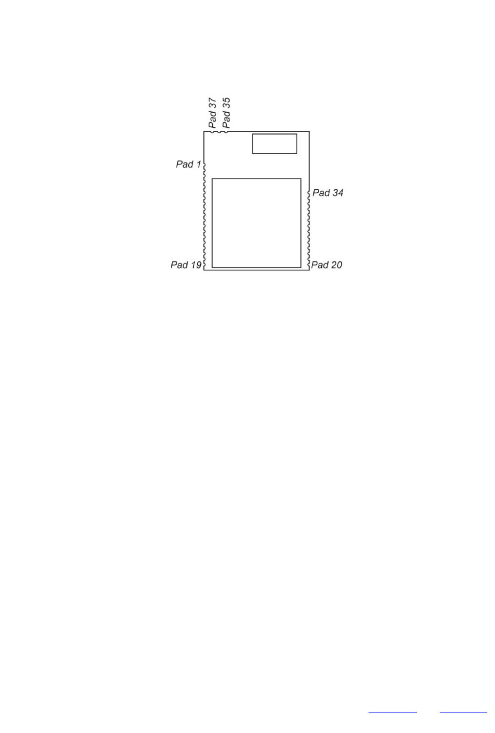
5 MECHANICAL CHARACTERISTICS
5.1 MODULE PAD DIAGRAM
Module pad connection diagram is depicted below (top view):
Fig. 5.1 Pad connection diagram for modules (top view)

© 2010 DiZiC Co. Ltd, 3F, N° 4-2 Jin Xi Street Taipei City 104, TAIWAN Email: info@dizic.com | Web: www.dizic.com
All Rights Reserved. All trademarks are property of their respective owners. Subject to change without notice.
Document ID: PB-ZB-MOD-003-20DS
5.2 MODULE PAD DESCRIPTION
The following table describes the pads of the module.
Table 5.1: Pad Description
Pad#
Signal
Direction
Description
1
GND
Power
Ground supply pad
2
GND
Power
Ground supply pad
3
VCC
Power
Power supply pad
4
VCC
Power
Power supply pad
5
nRESET
I
Active low chip reset (internal pull-up)
6
PC5
I/O
Digital I/O
TX_ACTIVE
O
Logic-level control for external Rx/Tx switch. The STM32W108 baseband
controls TX_ACTIVE and drives it high (VDD_PADS) when in Tx mode.
Select alternate output function with GPIO_PCCFGH[7:4]
7
PC6
I/O
Digital I/O
OSC32B
I/O
32.768 kHz crystal oscillator.
Select analogue function with GPIO_PCCFGH[11 :8]
nTX_ACTIVE
O
Inverted TX_ACTIVE signal (see PC5)
Select alternate output function with GPIO_PCCFGH[11:8]
8
PC7
I/O
Digital I/O
OSC32A
I/O
32.768 kHz crystal oscillator.
Select analogue function with GPIO_PCCFGH[15:12]
OSC32_EXT
I
Digital 32 kHz clock input source
9
PA7
I/O High current
Digital I/O Disable REG_EN with GPIO_DBGCFG[4]
TIM1CH4
O
Timer 1 Channel 4 output
Enable timer output with TIM1_CCER
Select alternate output function with GPIO_PACFGH[15:12]
Disable REG_EN with GPIO_DBGCFG[4]
I
Timer 1 Channel 4 input. Cannot be remapped
REG_EN
O
External regulator open drain output. (Enabled after reset).
10
PB3
I/O
Digital I/O
TIM2_CH3 (see
also Pad 13)
O
Timer 2 channel 3 output
Enable remap with TIM2_OR[6]
Enable timer output in TIM2_CCER
Select alternate output function with GPIO_PBCFGL[15:12]
I
Timer 2 channel 3 input Enable remap with TIM2_OR[6]
UART_CTS
I
UART CTS handshake of Serial Controller 1
Enable with SC1_UARTCFG[5]
Select UART with SC1_MODE
SC1SCLK
O
SPI master clock of Serial Controller 1 Either disable timer output in
TIM2_CCER, or disable remap with TIM2_OR[6] Enable master with
SC1_SPICFG[4] Select SPI with SC1_MODE
Select alternate output function with GPIO_PBCFGL[15:12]
I
SPI slave clock of Serial Controller 1
Enable slave with SC1_SPICFG[4]
Select SPI with SC1_MODE

© 2010 DiZiC Co. Ltd, 3F, N° 4-2 Jin Xi Street Taipei City 104, TAIWAN Email: info@dizic.com | Web: www.dizic.com
All Rights Reserved. All trademarks are property of their respective owners. Subject to change without notice.
Document ID: PB-ZB-MOD-003-20DS
Table 5.1: Pad Description (cont)
Pad#
Signal
Direction
Description
11
PB4
I/O
Digital I/O
TIM2_CH4 (see
also Pad 15)
O
Timer 2 channel 4 output
Enable remap with TIM2_OR[7]
Enable timer output in TIM2_CCER
Select alternate output function with GPIO_PBCFGH[3:0]
I
Timer 2 channel 4 input Enable remap with TIM2_OR[7]
UART_RTS
O
UART RTS handshake of Serial Controller 1
Either disable timer output in TIM2_CCER, or disable remap with
TIM2_OR[7]
Enable with SC1_UARTCFG[5] Select UART with SC1_MODE
Select alternate output function with GPIO_PBCFGH[3:0]
SC1nSSEL
I
SPI slave select of Serial Controller 1
Enable slave with SC1_SPICFG[4]
Select SPI with SC1_MODE
12
PA0
I/O
Digital I/O
TIM2_CH1 (see
also Pad 20)
O
Timer 2 channel 1 output
Disable remap with TIM2_OR[4]
Enable timer output in TIM2_CCER
Select alternate output function with GPIO_PACFGL[3:0]
I
Timer 2 channel 1 input
Disable remap with TIM2_OR[4]
SC2MOSI
O
SPI master data out of Serial Controller 2 Either disable timer output in
TIM2_CCER, or enable remap with TIM2_OR[4]
Enable master with SC2_SPICFG[4]
Select SPI with SC2_MODE
Select alternate output function with GPIO_PACFGL[3:0]
I
SPI slave data in of Serial Controller 2
Enable slave with SC2_SPICFG[4] Select
SPI with SC2_MODE
13
PA1
I/O
Digital I/O
TIM2_CH3 (see
also Pad 10)
O
Timer 2 channel 3 output
Disable remap with TIM2_OR[6]
Enable timer output in TIM2_CCER
Select alternate output function with GPIO_PACFGL[7:4]
I
Timer 2 channel 3 input Disable remap with TIM2_OR[6]
SC2SDA
I/O
TWI data of Serial Controller 2 Either disable timer output in TIM2_CCER, or
enable remap with TIM2_OR[6] Select TWI with SC2_MODE
Select alternate open-drain output function with GPIO_PACFGL[7:4]
SC2MISO
O
SPI slave data out of Serial Controller 2
Either disable timer output in TIM2_CCER, or enable remap with TIM2_OR[6]
Enable slave with SC2_SPICFG[4] Select SPI with SC2_MODE
Select alternate output function with GPIO_PACFGL[7:4]
I
SPI master data in of Serial Controller 2
Enable slave with SC2_SPICFG[4]
14
GND
Power
Ground supply pad.

© 2010 DiZiC Co. Ltd, 3F, N° 4-2 Jin Xi Street Taipei City 104, TAIWAN Email: info@dizic.com | Web: www.dizic.com
All Rights Reserved. All trademarks are property of their respective owners. Subject to change without notice.
Document ID: PB-ZB-MOD-003-20DS
Table 5.1: Pad Description (cont)
Pad#
Signal
Direction
Description
15
PA2
I/O
Digital I/O.
TIM2_CH4 (see
also Pad 11)
O
Timer 2 channel 4 output.
Disable remap with TIM2_OR[7].
Enable timer output in TIM2_CCER .
Select alternate output function with GPIO_PACFGL[11:8].
I
Timer 2 channel 4 input Disable remap with TIM2_OR[7].
SC2SCL
I/O
TWI clock of Serial Controller 2.
Either disable timer output in TIM2_CCER, or enable remap with TIM2_OR[7].
Select TWI with SC2_MODE.
Select alternate open-drain output function with GPIO_PACFGL[11:8].
SC2SCLK
O
SPI master clock of Serial Controller 2.
Either disable timer output in TIM2_CCER, or enable remap with TIM2_OR[7].
Enable master with SC2_SPICFG[4].
Select SPI with SC2_MODE.
Select alternate output function with GPIO_PACFGL[11:8].
I
SPI slave clock of Serial Controller 2.
Enable slave with SC2_SPICFG[4].
Select SPI with SC2_MODE.
16
PA3
I/O
Digital I/O
SC2nSSEL
I
SPI slave select of Serial Controller 2
Enable slave with SC2_SPICFG[4]
Select SPI with SC2_MODE
TRACECLK (see
also Pad 27)
O
Synchronous CPU trace clock .
Either disable timer output in TIM2_CCER, or enable remap with TIM2_OR[5].
Enable trace interface in ARM core.
Select alternate output function with GPIO_PACFGL[15:12].
TIM2_CH2 (see
also Pad 21)
O
Timer 2 channel 2 output.
Disable remap with TIM2_OR[5].
Enable timer output in TIM2_CCER.
Select alternate output function with GPIO_PACFGL[15:12].
I
Timer 2 channel 2 input Disable remap with TIM2_OR[5].
17
PA4
I/O
Digital I/O.
ADC4
Analog
ADC Input 4 Select analogue function with GPIO_PACFGH[3:0].
PTI_EN
O
Frame signal of Packet Trace Interface (PTI).
Disable trace interface in ARM core.
Select alternate output function with GPIO_PACFGH[3:0].
TRACEDATA2
O
Synchronous CPU trace data bit 2.
Select 4-wire synchronous trace interface in ARM core.
Enable trace interface in ARM core.
Select alternate output function with GPIO_PACFGH[3:0].
18
PA5
I/O
Digital I/O.
ADC5
Analog
ADC Inputs Select analog function with GPIO_PACFGH[7:4].
PTI_DATA
O
Data signal of Packet Trace Interface (PTI).
Disable trace interface in ARM core.
Select alternate output function with GPIO_PACFGH[7:4].
nBOOTMODE
I
Embedded serial boot-loader activation out of reset Signal is active during
and immediately after a reset on nRESET.
TRACEDATA3
O
Synchronous CPU trace data bit 3.
Select 4-wire synchronous trace interface in ARM core.
Enable trace interface in ARM core.
Select alternate output function with GPIO_PACFGH[7:4].
19
PA6
I/O High current
Digital I/O.
TIM1_CH3
O
Timer 1 channel 3 output.
Enable timer output in TIM1_CCER.
Select alternate output function with GPIO_PACFGH[11 :8].
I
Timer 1 channel 3 input Cannot be remapped.

© 2010 DiZiC Co. Ltd, 3F, N° 4-2 Jin Xi Street Taipei City 104, TAIWAN Email: info@dizic.com | Web: www.dizic.com
All Rights Reserved. All trademarks are property of their respective owners. Subject to change without notice.
Document ID: PB-ZB-MOD-003-20DS
Table 5.1: Pad Description (cont)
Pad#
Signal
Direction
Description
20
PB1
I/O
Digital I/O.
SC1MISO
O
SPI slave data out of Serial Controller 1.
Either disable timer output in TIM2_CCER, or disable remap with TIM2_OR[4].
Select SPI with SC1_MODE.
Select slave with SC1_SPICR.
Select alternate output function with GPIO_PBCFGL[7:4].
SC1MOSI
O
SPI master data out of Serial Controller 1.
Either disable timer output in TIM2_CCER, or disable remap with TIM2_OR[4].
Select SPI with SC1_MODE.
Select master with SC1_SPICR.
Select alternate output function with GPIO_PBCFGL[7:4]
SC1SDA
I/O
TWI data of Serial Controller 1.
Either disable timer output in TIM2_CCER, or disable remap with TIM2_OR[4].
Select TWI with SC1_MODE.
Select alternate open-drain output function with GPIO_PBCFGL[7:4].
SC1TXD
O
UART transmit data of Serial Controller 1.
Either disable timer output in TIM2_CCER, or disable remap
with TIM2_OR[4].
Select UART with SC1_MODE.
Select alternate output function with GPIO_PBCFGL[7:4].
TIM2_CH1 (see
also Pad 12)
O
Timer 2 channel 1 output.
Enable remap with TIM2_OR[4].
Enable timer output in TIM2_CCER.
Select alternate output function with GPIO_PACFGL[7:4].
I
Timer 2 channel 1 input Disable remap with TIM2_OR[4].
21
PB2
I/O
Digital I/O
SC1MISO
I
SPI master data in of Serial Controller 1.
Select SPI with SC1_MODE.
Select master with SC1_SPICR.
SC1MOSI
I
SPI slave data in of Serial Controller 1.
Select SPI with SC1_MODE.
Select slave with SC1_SPICR
SC1SCL
I/O
TWI clock of Serial Controller 1.
Either disable timer output in TIM2_CCER, or disable remap with TIM2_OR[5].
Select TWI with SC1_MODE.
Select alternate open-drain output function with GPIO_PBCFGL[11 :8].
SC1RXD
I
UART receive data of Serial Controller 1.
Select UART with SC1_MODE.
TIM2_CH2 (see
also Pad 16)
O
Timer 2 channel 2 output.
Enable remap with TIM2_OR[5].
Enable timer output in TIM2_CCER.
Select alternate output function with GPIO_PBCFGL[11 :8].
I
Timer 2 channel 2 input.
Enable remap with TIM2_OR[5].
22
SWCLK
I/O
Serial Wire clock input/output with debugger.
Selected when in Serial Wire mode (see JTMS description, Pad 26)
JTCK
1
JTAG clock input from debugger.
Selected when in JTAG mode (default mode, see JTMS description,
Pad 26) Internal pull-down is enabled.
23
PC2
I/O
Digital I/O.
Enable with GPIO_DBGCFG[5].
JTDO
O
JTAG data out to debugger.
Selected when in JTAG mode (default mode, see JTMS description,
Pad 26).
SWO
O
Serial Wire Output asynchronous trace output to debugger.
Select asynchronous trace interface in ARM core.
Enable trace interface in ARM core.
Select alternate output function with GPIO_PCCFGL[11:8].
Enable Serial Wire mode (see JTMS description, Pad 26).
Internal pull-up is enabled.

© 2010 DiZiC Co. Ltd, 3F, N° 4-2 Jin Xi Street Taipei City 104, TAIWAN Email: info@dizic.com | Web: www.dizic.com
All Rights Reserved. All trademarks are property of their respective owners. Subject to change without notice.
Document ID: PB-ZB-MOD-003-20DS
Table 5.1: Pad Description (cont)
Pad#
Signal
Direction
Description
24
PC3
I/O
Digital I/O Either Enable with GPIO_DBGCFG[5], or enable Serial Wire mode
(see JTMS description, Pad 26)
JTDI
1
JTAG data in from debugger Selected when in JTAG mode (default
mode, see JTMS description, Pad 26).
Internal pull-up is enabled.
25
GND
Power
Ground supply pad.
26
PC4
I/O
Digital I/O Enable with GPIO_DBGCFG[5]
JTMS
I
JTAG mode select from debugger.
Selected when in JTAG mode (default mode).
JTAG mode is enabled after power-up or by forcing nRESET low.
Select Serial Wire mode using the ARM-defined protocol through a debugger.
Internal pull-up is enabled.
SWDIO
I/O
Serial Wire bidirectional data to/from debugger.
Enable Serial Wire mode (see JTMS description).
Select Serial Wire mode using the ARM-defined protocol through a
debugger.
Internal pull-up is enabled.
27
PB0
I/O
Digital I/O
VREF
Analog O
ADC reference output.
Enable analog function with GPIO_PBCFGL[3:0]
VREF
Analog I
ADC reference input.
Enable analog function with GPIO_PBCFGL[3:0].
Enable reference output with an STM system function
IRQA
I
External interrupt source A.
TRACECLK (see
also Pad 16)
O
Synchronous CPU trace clock.
Enable trace interface in ARM core.
Select alternate output function with GPIO_PBCFGL[3:0].
TIM1CLK
I
Timer 1 external clock input
TIM2MSK
I
Timer 2 external clock mask input
28
GND
Power
Ground supply pad.
29
PC1
I/O
Digital I/O
ADC3
Analog
ADC Inputs Enable analog function with GPIO_PCCFGL[7:4]
SWO (see also
Pad 23)
O
Serial Wire Output asynchronous trace output to debugger.
Select asynchronous trace interface in ARM core.
Enable trace interface in ARM core.
Select alternate output function with GPIO_PCCFGL[7:4].
TRACEDATA0
O
Synchronous CPU trace data bit 0.
Select 1-, 2- or 4-wire synchronous trace interface in ARM core.
Enable trace interface in ARM core.
Select alternate output function with GPIO_PCCFGL[7:4].
30
PC0
I/O High current
Digital I/O.
Either enable with GPIO_DBGCFG[5], or enable Serial Wire mode (see
JTMS description, Pad 26) and disable TRACEDATA1.
JRST
I
JTAG reset input from debugger.
Selected when in JTAG mode (default mode, see JTMS description) and
TRACEDATA1 is disabled.
Internal pull-up is enabled.
IRQD1
I
Default external interrupt source D
TRACEDATA1
O
Synchronous CPU trace data bit 1.
Select 2- or 4-wire synchronous trace interface in ARM core.
Enable trace interface in ARM core.
Select alternate output function with GPIO_PCCFGL[3:0].
© 2010 DiZiC Co. Ltd, 3F, N° 4-2 Jin Xi Street Taipei City 104, TAIWAN Email: info@dizic.com | Web: www.dizic.com
All Rights Reserved. All trademarks are property of their respective owners. Subject to change without notice.
Document ID: PB-ZB-MOD-003-20DS
Table 5.1: Pad Description (cont)
Pad#
Signal
Direction
Description
31
PB7
I/O High current
Digital I/O
ADC2
Analog
ADC Input 2
Enable analog function with GPIO_PBCFGH[15:12]
IRQC1
I
Default external interrupt source C
TIM1_CH2
O
Timer 1 channel 2 output.
Enable timer output in TIM1_CCER.
Select alternate output function with GPIO_PBCFGH[15:12].
I
Timer 1 channel 2 input .(Cannot be remapped).
32
PB6
I/O High current
Digital I/O.
ADC1
Analog
ADC Input 1.
Enable analog function with GPIO_PBCFGH[11:8].
IRQB
I
External interrupt source B.
TIM1_CH1
O
Timer 1 channel 1 output.
Enable timer output in TIM1_CCER.
Select alternate output function with GPIO_PBCFGH[11:8].
I
Timer 1 channel 1 input. (Cannot be remapped).
33
PB5
I/O
Digital I/O
ADC0
Analog
ADC Input 0.
Enable analog function with GPIO_PBCFGH[7:4].
TIM2CLK
I
Timer 2 external clock input.
TIM1MSK
I
Timer 2 external clock mask input.
34
GND
Power
Ground supply pad.
35
GNDRF
RF Ground
Ground pad for RF port.
36
RF
Analog
RF port with 50 Ohm impedance.
37
GNDRF
RF Ground
Ground pad for RF port.
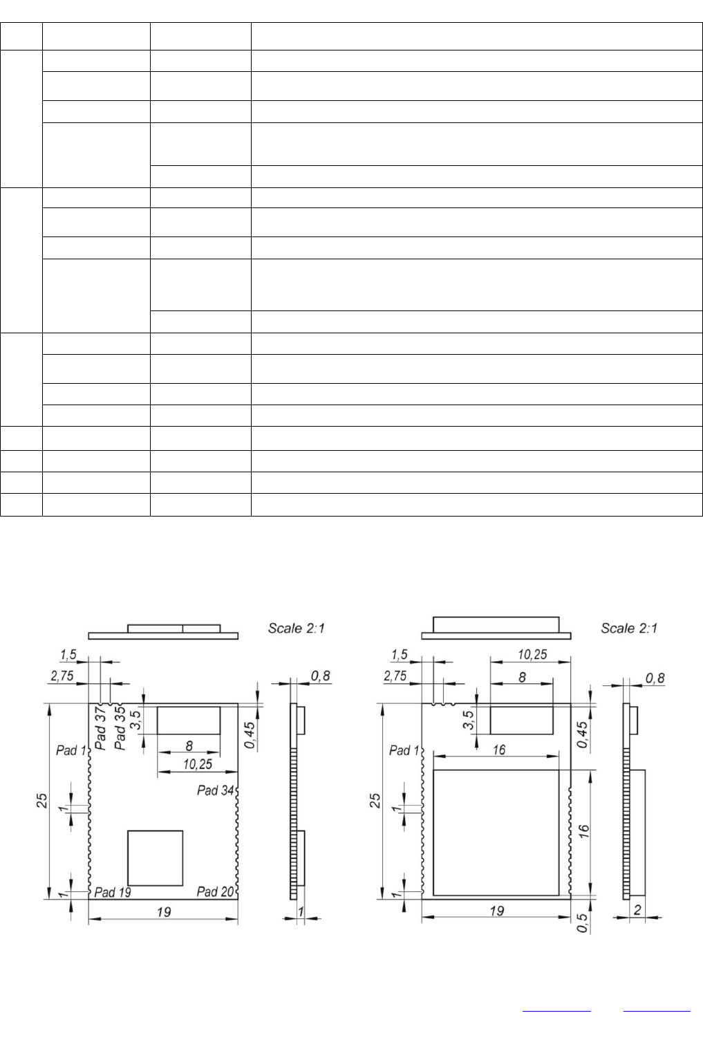
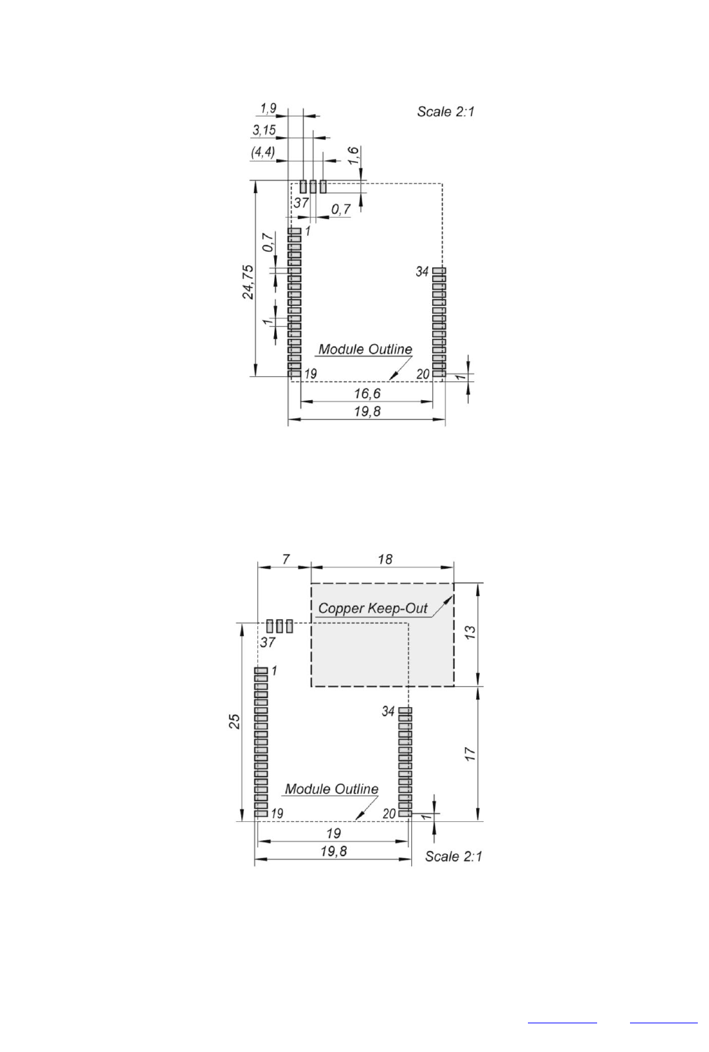
5.3 PACKAGE MECHANICAL DIMENSIONS
Module dimensions are 25 mm x 19 mm x 2 mm and detailed drawing is shown below on Fig. 5.2.
Fig. 5.2 Dimensions of the module. Left: EMI Option “S” -- without shielding; Right: Option “M” – with metal shielding
(Enhanced EMI protection)
© 2010 DiZiC Co. Ltd, 3F, N° 4-2 Jin Xi Street Taipei City 104, TAIWAN Email: info@dizic.com | Web: www.dizic.com
All Rights Reserved. All trademarks are property of their respective owners. Subject to change without notice.
Document ID: PB-ZB-MOD-003-20DS
6 SOLDERING
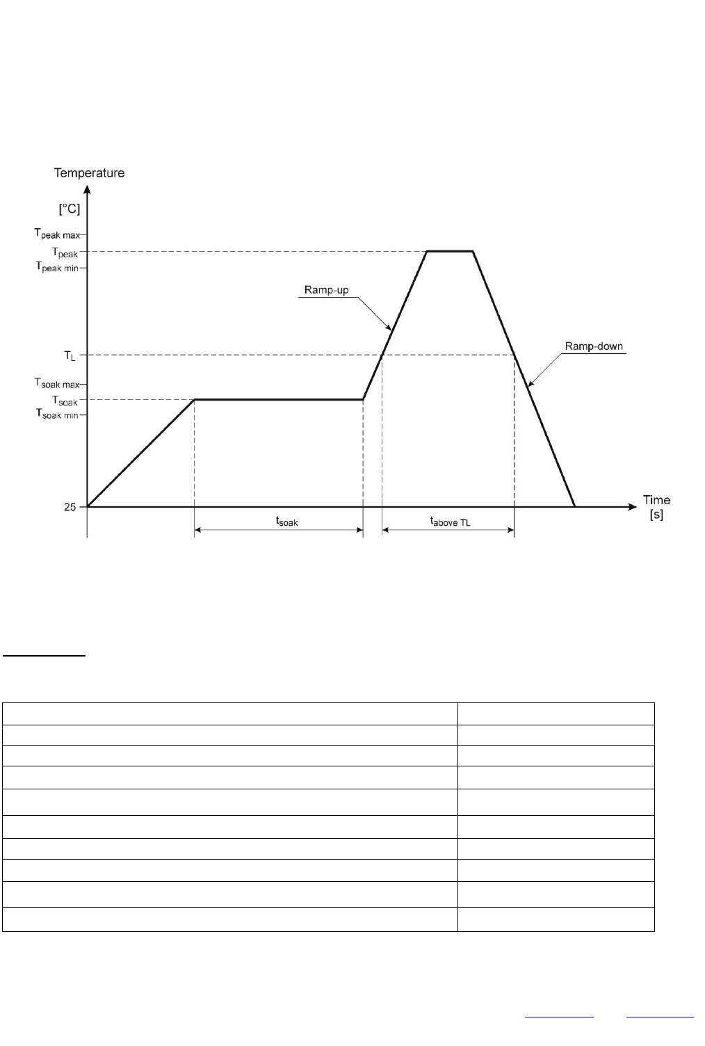
6.1 SOLDER TEMPERATURE PROFILE
The following Fig. 6.1 illustrates the solder temperature profile for the module. This temperature profile is similar for other
RoHS compliant packages, but manufacturing lines should be programmed with this profile in order to guarantee proper solder
connection to the PCB. Please note: module can be soldered only once.
Reflow Profile
Fig. 6.1 Reflow profile
6.2 PROFILE PARAMETERS
The following table 6.1 contains the temperature profile parameters.
Important note: module should be processed according to recommended temperature profile only one time.
Table 6.1 Solder Reflow Parameters
Parameter
Value
Average Ramp Up Rate (from Tsoakmax to Tpeak)
3°C per second max
Average Ramp Up Rate (from 25°C to Tsoakmin)
2°C to 4°C per second max
Minimum Soak Temperature (Tsoakmjn)
150°C
Maximum Soak Temperature (Tsoakmax)
200°C
TL
220°C
Time above TL
30 to 60 seconds
Minimum Peak Temperature Tpeakmin
230°C
Maximum Peak Temperature Tpeakmax
250°C
Ramp Down Rate
6°C per second max
© 2010 DiZiC Co. Ltd, 3F, N° 4-2 Jin Xi Street Taipei City 104, TAIWAN Email: info@dizic.com | Web: www.dizic.com
All Rights Reserved. All trademarks are property of their respective owners. Subject to change without notice.
Document ID: PB-ZB-MOD-003-20DS
6.3 RECOMMENDED FOOTPRINT
Top view of recommended footprint for module is shown below on Fig. 6.2:
Fig. 6.2 Recommended footprint for modules (top view)
For the modules with output option “A” (with Embedded SMD Antenna) it is important to prevent presence of any conductive
materials in proximity of the module’s antenna. This requirement is valid for copper traces, ground planes, wires and
connectors too. Recommended “Copper-Keep-Out” area, where presence of copper (and any conductive material too) should
be avoided is depicted on Fig. 6.3 below:
Fig. 6.3 Recommended “Copper-Keep-Out” Area (top view) – only for modules with Output Option “A”

© 2010 DiZiC Co. Ltd, 3F, N° 4-2 Jin Xi Street Taipei City 104, TAIWAN Email: info@dizic.com | Web: www.dizic.com
All Rights Reserved. All trademarks are property of their respective owners. Subject to change without notice.
Document ID: PB-ZB-MOD-003-20DS
7 ORDERING INFORMATION
Example: DZ - ZB - P - O - S - E -
Manufactured by DiZiC
ZigBee Module
Power level options
S -- Standard + 7dBm
R -- Front End with RF Output Power Level Detector + 20 dBm
T -- Front End + 20 dBm
Output options:
A -- Embedded SMD Antenna
P -- Single ended 50 Ohm RF Pad
U -- U.FL 50 Ohm coaxial connector
Stack options:
F -- RF4CE stack
X -- Proprietary stack
Z -- EmberZNet PRO stack
Electromagnetic Interference (EMI) protection options:
S -- Standard, without protective metal shielding
M -- Metal Shield, for enhanced EMI protection

© 2010 DiZiC Co. Ltd, 3F, N° 4-2 Jin Xi Street Taipei City 104, TAIWAN Email: info@dizic.com | Web: www.dizic.com
All Rights Reserved. All trademarks are property of their respective owners. Subject to change without notice.
Document ID: PB-ZB-MOD-003-20DS
8 LIST OF ACRONYMS
This chapter defines a collection of terms that are commonly used when talking about networks in general or ZigBee in
particular.
AC Alternating Current
ACK Acknowledge
ADC Analogue-to-Digital Converter
API Application Programming Interface
ARM Advanced RISC Machines Ltd, now ARM Holdings
BiCMOS Bipolar junction transistors combined with CMOS technology
BER Bit Error Rate
CMOS Complementary Metal–Oxide–Semiconductor
CPU Central Processing Unit
CTS Clear To Send
dB decibel, logarithmic unit of measurement that expresses the magnitude of a physical quantity
dBm Power ratio in decibels of the measured power referenced to one milliwatt (1 mW)
DC Direct Current
DWT Data Watch-point and Trace
EEPROM Electrically Erasable Programmable Read-Only Memory
EMI Electromagnetic Interference
ESD Electrostatic Discharge
FE Front End
FPB Flash Patch and Breakpoint
GPIO General Purpose Input/Output
HAL Hardware Abstraction Layer
HBM Human Body Model
HF High Frequency
HVAC Heating, Ventilating and Air Conditioning
I²C Inter-Integrated Circuit bus
IEEE Institute of Electrical and Electronics Engineers
IRQ Interrupt Request
ISM Industrial, Scientific and Medical radio band
ITM Instrumentation Trace Macrocell
JTAG Joint Test Action Group, digital interface for debugging of embedded device
LNA Low Noise Amplifier
MAC Media Access Control layer
MCU Microcontroller Unit
MPU Multi-core Processing Unit
PA Power Amplifier
PCB Printed Circuit Board
PER Package Error Ratio
PSD Power Spectral Density
PTI Packet Trace Interface
RAM Random Access Memory
RF Radio Frequency
RF4CE Radio Frequency for Consumer Electronics consortium
RSSI Received Signal Strength Indicator
RX Receiver
SMD Surface Mounted Device
SPI Serial Peripheral Interface
STM STMicroelectronics, an Italian-French electronics and semiconductor manufacturer
TWI Two Wire Interface, a variant of I²C
TX Transmitter
UART Universal Asynchronous Receiver/Transmitter
U.FL Miniature coaxial RF connector (up to 6 GHz) manufactured by Hirose Electric Group in Japan
VCO Voltage Controlled Oscillator
ZigBee, ZigBee PRO Wireless networking standards targeted at low-power applications
802.15.4 The IEEE 802.15.4-2003 standard applicable to low-rate wireless Personal Area Network

© 2010 DiZiC Co. Ltd, 3F, N° 4-2 Jin Xi Street Taipei City 104, TAIWAN Email: info@dizic.com | Web: www.dizic.com
All Rights Reserved. All trademarks are property of their respective owners. Subject to change without notice.
Document ID: PB-ZB-MOD-003-20DS
9 REFERENCES & REVISION HISTORY
[1]. STM32W108HB, STM32W108CB, High-performance, 802.15.4 wireless system-on-chip, Data brief, 20-Aug-2009, Rev. 1
[2]. STM32W108HB, STM32W108CB, High-performance, 802.15.4 wireless system-on-chip, Preliminary data, 01-Mar-2010,
Rev. 4
[3]. RN0034, Release notes, STM32W108xx starter and extension kits EmberZNet 4.0.2 GA, Doc ID 16225, 16-Feb-2010,
Rev. 2
[4]. RN0047, Release notes, STM32W108xx starter and extension kits ZigBee RF4CE, Doc ID 17098, 23-Feb-2010, Rev. 1
[5]. RN0046, Release note, STM32W108xx starter and extension kits for Simple MAC library, Doc ID 16996, 04-March-2010,
Rev. 1
[6]. UM0894, User Manual, STM32W-SK and STM32W-EXT starter and extension kits for STM32W108xx, Doc ID 16999, 05-
Feb-2010, Rev. 1
[7]. UM0847, User Manual, IAR customization for STM32W108 system-on-chip, Doc ID 16551, 16-Nov-2009, Rev. 1.